EP4509645A1 - Substrate for electronic devices and method for producing same - Google Patents
Substrate for electronic devices and method for producing same Download PDFInfo
- Publication number
- EP4509645A1 EP4509645A1 EP23788038.0A EP23788038A EP4509645A1 EP 4509645 A1 EP4509645 A1 EP 4509645A1 EP 23788038 A EP23788038 A EP 23788038A EP 4509645 A1 EP4509645 A1 EP 4509645A1
- Authority
- EP
- European Patent Office
- Prior art keywords
- substrate
- silicon single
- crystal
- crystal substrate
- bonded
- Prior art date
- Legal status (The legal status is an assumption and is not a legal conclusion. Google has not performed a legal analysis and makes no representation as to the accuracy of the status listed.)
- Pending
Links
Images


Classifications
-
- H—ELECTRICITY
- H10—SEMICONDUCTOR DEVICES; ELECTRIC SOLID-STATE DEVICES NOT OTHERWISE PROVIDED FOR
- H10P—GENERIC PROCESSES OR APPARATUS FOR THE MANUFACTURE OR TREATMENT OF DEVICES COVERED BY CLASS H10
- H10P14/00—Formation of materials, e.g. in the shape of layers or pillars
- H10P14/20—Formation of materials, e.g. in the shape of layers or pillars of semiconductor materials
- H10P14/29—Formation of materials, e.g. in the shape of layers or pillars of semiconductor materials characterised by the substrates
- H10P14/2926—Crystal orientations
-
- H—ELECTRICITY
- H10—SEMICONDUCTOR DEVICES; ELECTRIC SOLID-STATE DEVICES NOT OTHERWISE PROVIDED FOR
- H10W—GENERIC PACKAGES, INTERCONNECTIONS, CONNECTORS OR OTHER CONSTRUCTIONAL DETAILS OF DEVICES COVERED BY CLASS H10
- H10W46/00—Marks applied to devices, e.g. for alignment or identification
-
- C—CHEMISTRY; METALLURGY
- C30—CRYSTAL GROWTH
- C30B—SINGLE-CRYSTAL GROWTH; UNIDIRECTIONAL SOLIDIFICATION OF EUTECTIC MATERIAL OR UNIDIRECTIONAL DEMIXING OF EUTECTOID MATERIAL; REFINING BY ZONE-MELTING OF MATERIAL; PRODUCTION OF A HOMOGENEOUS POLYCRYSTALLINE MATERIAL WITH DEFINED STRUCTURE; SINGLE CRYSTALS OR HOMOGENEOUS POLYCRYSTALLINE MATERIAL WITH DEFINED STRUCTURE; AFTER-TREATMENT OF SINGLE CRYSTALS OR A HOMOGENEOUS POLYCRYSTALLINE MATERIAL WITH DEFINED STRUCTURE; APPARATUS THEREFOR
- C30B25/00—Single-crystal growth by chemical reaction of reactive gases, e.g. chemical vapour-deposition growth
- C30B25/02—Epitaxial-layer growth
- C30B25/18—Epitaxial-layer growth characterised by the substrate
- C30B25/183—Epitaxial-layer growth characterised by the substrate being provided with a buffer layer, e.g. a lattice matching layer
-
- C—CHEMISTRY; METALLURGY
- C30—CRYSTAL GROWTH
- C30B—SINGLE-CRYSTAL GROWTH; UNIDIRECTIONAL SOLIDIFICATION OF EUTECTIC MATERIAL OR UNIDIRECTIONAL DEMIXING OF EUTECTOID MATERIAL; REFINING BY ZONE-MELTING OF MATERIAL; PRODUCTION OF A HOMOGENEOUS POLYCRYSTALLINE MATERIAL WITH DEFINED STRUCTURE; SINGLE CRYSTALS OR HOMOGENEOUS POLYCRYSTALLINE MATERIAL WITH DEFINED STRUCTURE; AFTER-TREATMENT OF SINGLE CRYSTALS OR A HOMOGENEOUS POLYCRYSTALLINE MATERIAL WITH DEFINED STRUCTURE; APPARATUS THEREFOR
- C30B29/00—Single crystals or homogeneous polycrystalline material with defined structure characterised by the material or by their shape
- C30B29/10—Inorganic compounds or compositions
- C30B29/40—AIIIBV compounds wherein A is B, Al, Ga, In or Tl and B is N, P, As, Sb or Bi
- C30B29/403—AIII-nitrides
-
- C—CHEMISTRY; METALLURGY
- C30—CRYSTAL GROWTH
- C30B—SINGLE-CRYSTAL GROWTH; UNIDIRECTIONAL SOLIDIFICATION OF EUTECTIC MATERIAL OR UNIDIRECTIONAL DEMIXING OF EUTECTOID MATERIAL; REFINING BY ZONE-MELTING OF MATERIAL; PRODUCTION OF A HOMOGENEOUS POLYCRYSTALLINE MATERIAL WITH DEFINED STRUCTURE; SINGLE CRYSTALS OR HOMOGENEOUS POLYCRYSTALLINE MATERIAL WITH DEFINED STRUCTURE; AFTER-TREATMENT OF SINGLE CRYSTALS OR A HOMOGENEOUS POLYCRYSTALLINE MATERIAL WITH DEFINED STRUCTURE; APPARATUS THEREFOR
- C30B33/00—After-treatment of single crystals or homogeneous polycrystalline material with defined structure
- C30B33/06—Joining of crystals
-
- H—ELECTRICITY
- H10—SEMICONDUCTOR DEVICES; ELECTRIC SOLID-STATE DEVICES NOT OTHERWISE PROVIDED FOR
- H10D—INORGANIC ELECTRIC SEMICONDUCTOR DEVICES
- H10D62/00—Semiconductor bodies, or regions thereof, of devices having potential barriers
- H10D62/40—Crystalline structures
- H10D62/405—Orientations of crystalline planes
-
- H—ELECTRICITY
- H10—SEMICONDUCTOR DEVICES; ELECTRIC SOLID-STATE DEVICES NOT OTHERWISE PROVIDED FOR
- H10D—INORGANIC ELECTRIC SEMICONDUCTOR DEVICES
- H10D86/00—Integrated devices formed in or on insulating or conducting substrates, e.g. formed in silicon-on-insulator [SOI] substrates or on stainless steel or glass substrates
- H10D86/201—Integrated devices formed in or on insulating or conducting substrates, e.g. formed in silicon-on-insulator [SOI] substrates or on stainless steel or glass substrates the substrates comprising an insulating layer on a semiconductor body, e.g. SOI
-
- H—ELECTRICITY
- H10—SEMICONDUCTOR DEVICES; ELECTRIC SOLID-STATE DEVICES NOT OTHERWISE PROVIDED FOR
- H10P—GENERIC PROCESSES OR APPARATUS FOR THE MANUFACTURE OR TREATMENT OF DEVICES COVERED BY CLASS H10
- H10P14/00—Formation of materials, e.g. in the shape of layers or pillars
- H10P14/20—Formation of materials, e.g. in the shape of layers or pillars of semiconductor materials
- H10P14/29—Formation of materials, e.g. in the shape of layers or pillars of semiconductor materials characterised by the substrates
- H10P14/2901—Materials
- H10P14/2902—Materials being Group IVA materials
- H10P14/2905—Silicon, silicon germanium or germanium
-
- H—ELECTRICITY
- H10—SEMICONDUCTOR DEVICES; ELECTRIC SOLID-STATE DEVICES NOT OTHERWISE PROVIDED FOR
- H10P—GENERIC PROCESSES OR APPARATUS FOR THE MANUFACTURE OR TREATMENT OF DEVICES COVERED BY CLASS H10
- H10P14/00—Formation of materials, e.g. in the shape of layers or pillars
- H10P14/20—Formation of materials, e.g. in the shape of layers or pillars of semiconductor materials
- H10P14/32—Formation of materials, e.g. in the shape of layers or pillars of semiconductor materials characterised by intermediate layers between substrates and deposited layers
- H10P14/3202—Materials thereof
- H10P14/3204—Materials thereof being Group IVA semiconducting materials
- H10P14/3211—Silicon, silicon germanium or germanium
-
- H—ELECTRICITY
- H10—SEMICONDUCTOR DEVICES; ELECTRIC SOLID-STATE DEVICES NOT OTHERWISE PROVIDED FOR
- H10P—GENERIC PROCESSES OR APPARATUS FOR THE MANUFACTURE OR TREATMENT OF DEVICES COVERED BY CLASS H10
- H10P14/00—Formation of materials, e.g. in the shape of layers or pillars
- H10P14/20—Formation of materials, e.g. in the shape of layers or pillars of semiconductor materials
- H10P14/32—Formation of materials, e.g. in the shape of layers or pillars of semiconductor materials characterised by intermediate layers between substrates and deposited layers
- H10P14/3202—Materials thereof
- H10P14/3238—Materials thereof being insulating materials
-
- H—ELECTRICITY
- H10—SEMICONDUCTOR DEVICES; ELECTRIC SOLID-STATE DEVICES NOT OTHERWISE PROVIDED FOR
- H10P—GENERIC PROCESSES OR APPARATUS FOR THE MANUFACTURE OR TREATMENT OF DEVICES COVERED BY CLASS H10
- H10P14/00—Formation of materials, e.g. in the shape of layers or pillars
- H10P14/20—Formation of materials, e.g. in the shape of layers or pillars of semiconductor materials
- H10P14/32—Formation of materials, e.g. in the shape of layers or pillars of semiconductor materials characterised by intermediate layers between substrates and deposited layers
- H10P14/3242—Structure
- H10P14/3244—Layer structure
- H10P14/3248—Layer structure consisting of two layers
-
- H—ELECTRICITY
- H10—SEMICONDUCTOR DEVICES; ELECTRIC SOLID-STATE DEVICES NOT OTHERWISE PROVIDED FOR
- H10P—GENERIC PROCESSES OR APPARATUS FOR THE MANUFACTURE OR TREATMENT OF DEVICES COVERED BY CLASS H10
- H10P14/00—Formation of materials, e.g. in the shape of layers or pillars
- H10P14/20—Formation of materials, e.g. in the shape of layers or pillars of semiconductor materials
- H10P14/32—Formation of materials, e.g. in the shape of layers or pillars of semiconductor materials characterised by intermediate layers between substrates and deposited layers
- H10P14/3258—Crystal orientation
-
- H—ELECTRICITY
- H10—SEMICONDUCTOR DEVICES; ELECTRIC SOLID-STATE DEVICES NOT OTHERWISE PROVIDED FOR
- H10P—GENERIC PROCESSES OR APPARATUS FOR THE MANUFACTURE OR TREATMENT OF DEVICES COVERED BY CLASS H10
- H10P14/00—Formation of materials, e.g. in the shape of layers or pillars
- H10P14/20—Formation of materials, e.g. in the shape of layers or pillars of semiconductor materials
- H10P14/34—Deposited materials, e.g. layers
- H10P14/3402—Deposited materials, e.g. layers characterised by the chemical composition
- H10P14/3414—Deposited materials, e.g. layers characterised by the chemical composition being group IIIA-VIA materials
- H10P14/3416—Nitrides
-
- H—ELECTRICITY
- H10—SEMICONDUCTOR DEVICES; ELECTRIC SOLID-STATE DEVICES NOT OTHERWISE PROVIDED FOR
- H10P—GENERIC PROCESSES OR APPARATUS FOR THE MANUFACTURE OR TREATMENT OF DEVICES COVERED BY CLASS H10
- H10P90/00—Preparation of wafers not covered by a single main group of this subclass, e.g. wafer reinforcement
- H10P90/19—Preparing inhomogeneous wafers
- H10P90/1904—Preparing vertically inhomogeneous wafers
- H10P90/1906—Preparing SOI wafers
- H10P90/1914—Preparing SOI wafers using bonding
-
- H—ELECTRICITY
- H10—SEMICONDUCTOR DEVICES; ELECTRIC SOLID-STATE DEVICES NOT OTHERWISE PROVIDED FOR
- H10W—GENERIC PACKAGES, INTERCONNECTIONS, CONNECTORS OR OTHER CONSTRUCTIONAL DETAILS OF DEVICES COVERED BY CLASS H10
- H10W10/00—Isolation regions in semiconductor bodies between components of integrated devices
- H10W10/10—Isolation regions comprising dielectric materials
- H10W10/181—Semiconductor-on-insulator [SOI] isolation regions, e.g. buried oxide regions of SOI wafers
-
- H—ELECTRICITY
- H10—SEMICONDUCTOR DEVICES; ELECTRIC SOLID-STATE DEVICES NOT OTHERWISE PROVIDED FOR
- H10W—GENERIC PACKAGES, INTERCONNECTIONS, CONNECTORS OR OTHER CONSTRUCTIONAL DETAILS OF DEVICES COVERED BY CLASS H10
- H10W46/00—Marks applied to devices, e.g. for alignment or identification
- H10W46/201—Marks applied to devices, e.g. for alignment or identification located on the periphery of wafers, e.g. orientation notches or lot numbers
Definitions
- the present invention relates to a substrate for an electronic device and a method for producing the same, in particular, a substrate for an electronic device where a nitride semiconductor is formed on a silicon substrate and a method for producing the same.
- Nitride semiconductors including GaN and AlN, can be used for fabricating high electron mobility transistors (HEMT) that uses two-dimensional electron gas and electronic devices with a high breakdown voltage.
- HEMT high electron mobility transistors
- a nitride semiconductor wafer having a nitride semiconductor grown on a substrate It is difficult to produce a nitride semiconductor wafer having a nitride semiconductor grown on a substrate, and a sapphire substrate or a SiC substrate is conventionally used as a growth substrate.
- a sapphire substrate or a SiC substrate is conventionally used as a growth substrate.
- epitaxial growth of a nitride semiconductor by vapor phase growth on a silicon single-crystal substrate has been employed.
- Patent Document 1 discloses the thickness of a bonded substrate of 2 mm or more.
- Patent Document 2 discloses a combination of two substrates to be bonded, including a bond wafer having a plane orientation of ⁇ 111 ⁇ and a base wafer having a plane orientation of ⁇ 100 ⁇ and a resistivity of 0.1 Qcm or less.
- the use of bonded substrates as growth substrates is known as disclosed in Patent Document 1 and Patent Document 2.
- the slips, the cracks, and the like have often been generated mainly at a notch portion of the substrates.
- the notch is formed in ⁇ 110> direction on the ⁇ 111 ⁇ silicon single-crystal substrate and formed in ⁇ 110> direction or ⁇ 100> direction on a ⁇ 100 ⁇ silicon single-crystal substrate.
- An object of the present invention is to provide a substrate for an electronic device, including a nitride semiconductor formed on a silicon single-crystal, which is the substrate for the electronic device with the suppressed generation of the slips, the cracks, etc., and with high breaking strength, and a method for producing the substrate.
- the present invention provides a substrate for an electronic device, comprising a nitride semiconductor film formed on a bonded substrate comprising a silicon single crystal, wherein
- a cleavage plane with respect to the main surface is nonvertical (the cleavage plane is tilted) by providing the off-angle as in the second silicon single-crystal substrate of the present invention, instead of a just-crystal-plane-orientation substrate without the off-angle like a conventional second silicon single-crystal substrate.
- the cleavage plane being tilted of just one second silicon single-crystal substrate can make the substrate for the electronic device with a high breaking strength, in which an increase in warps and generation of slips, cracks (hereinafter also referred to as cracks, etc.) are suppressed compared with a conventional substrate where the cleavage plane of the second silicon single-crystal substrate is also vertical to a bonding surface.
- the second silicon single-crystal substrate can be nitrogen-doped.
- Such a substrate serves as the substrate for the electronic device having higher breaking strength.
- the first silicon single-crystal substrate is formed with a notch in ⁇ 110> direction
- Such a substrate serves as the substrate for an electronic device, with further suppressed generation of the cracks, etc., and with high breaking strength, due to a positional relationship between the cleavage planes of the to-be-bonded first silicon single-crystal substrate and the to-be-bonded second silicon single-crystal substrate.
- the bonded substrate can have a diameter of 300 mm or larger.
- the substrate having the high breaking strength of the present invention is particularly effective for the substrate for the electronic device having a large diameter, such as a diameter of 300 mm or larger.
- the present invention provides a method for producing a substrate for an electronic device by forming a nitride semiconductor film on a bonded substrate comprising a silicon single crystal, the method comprising the steps of:
- the second silicon single-crystal substrate having the cleavage plane tilted to the bonding surface is included, and thus, the substrate for the electronic device with suppressed generation of the cracks, etc., and with high breaking strength can be produced.
- the second silicon single-crystal substrate to be prepared can be nitrogen-doped.
- the substrate for the electronic device having higher breaking strength can be produced.
- the first silicon single-crystal substrate to be prepared is formed with a notch in ⁇ 110> direction
- first silicon single-crystal substrate and the second silicon single-crystal substrate to be prepared can have diameters of 300 mm or larger.
- the substrate having a high breaking strength such as the substrate for the electronic device produced by the inventive producing method, is particularly effective for producing the substrate for the electronic device having a large diameter, such as a diameter of 300 mm or larger.
- the second silicon single-crystal substrate has an off-angle and a cleavage plane tilted to the bonding surface, and thus, the substrate for the electronic device with the suppressed generation of the cracks, etc., and with high breaking strength can be provided.
- a nitride semiconductor film 21 is formed on a silicon single-crystal bonded substrate 10.
- the silicon single-crystal bonded substrate 10 is also referred to simply as "bonded substrate.”
- the bonded substrate 10 is a substrate in which a first silicon single-crystal substrate 11 having a crystal plane orientation of ⁇ 111 ⁇ and a second silicon single-crystal substrate 12 having a main surface that has an off-angle with respect to a crystal plane orientation of ⁇ 100 ⁇ are bonded via an oxide film 13.
- the nitride semiconductor film 21 is formed on the first silicon single-crystal substrate 11.
- ⁇ means a general term for equivalent crystal plane orientations, and () means each direction of the crystal plane orientations.
- ⁇ > indicates a general term for equivalent crystal axis directions, and [] means each direction of crystal axis directions.
- the silicon single-crystal substrate may be thickened and epitaxial growth may be performed.
- bonding of two silicon single-crystal substrates has been conducted; however, even if the bonded substrate is used, a complete suppression of the cracks, etc., has not been achieved.
- the substrate for the electronic device 20 as described above, two silicon single-crystal substrates, the first and second silicon single-crystal substrates 11 and 12, being bonded, are used as an underlying substrate (seed crystal) (bonded substrate 10); moreover, in the second silicon single-crystal substrate 12 among them, the main surface has the off-angle with respect to the crystal plane orientation of ⁇ 100 ⁇ , thus a cleavage plane is nonvertical with respect to a bonding surface with the first silicon single-crystal substrate.
- the substrate for the electronic device can be made with suppressed generation of the crack, etc. (increased warps, or slips, cracks) and with high breaking strength.
- FIG. 2 shows an example of a positional relationship between the cleavage plane in the first silicon single-crystal substrate 11 and the cleavage plane in the second silicon single-crystal substrate 12.
- these cleavage planes are in close positions with each other in a vertical direction to the main surface
- the present invention is not limited to such a positional relationship.
- a case having the off-angle in the left-and-right direction on a paper is given as an example in FIG. 2
- the direction of the off-angle is not particularly limited in the present invention.
- both substrates are just-crystal-plane-orientation substrates without the off-angle; the cracks, etc., are prone to be generated.
- the size of the off-angle is not particularly limited but can be, for example, more than 0° and 12° or less, preferably from 2° to 8°, particularly 4°.
- each position of forming notch of the first silicon single-crystal substrate 11 and the second silicon single-crystal substrate 12 is not particularly limited.
- the first silicon single-crystal substrate 11 is formed with the notch in ⁇ 110> direction
- the second silicon single-crystal substrate 12 is formed with the notch in ⁇ 110> direction.
- the bonded substrate 10 is bonded so as to align the notch position of the first silicon single-crystal substrate 11 and the notch position of the second silicon single-crystal substrate 12.
- the breaking strength can be further improved by the positional shift between the cleavage planes of the first silicon single-crystal substrate and the second silicon single-crystal substrate in the planar view.
- FIG. 3 a drawing seen from the main surface (main front surface) side of each substrate.
- the substrate having the crystal plane orientation of ⁇ 111 ⁇ and the notch at ⁇ 110> position is the first silicon single-crystal substrate 11 and the substrate having the crystal plane orientation of ⁇ 100 ⁇ and the notch at ⁇ 110> position is the second silicon single-crystal substrate 12, is described.
- the cleavage plane of the first silicon single-crystal substrate 11 is schematically shown by a dotted line
- the cleavage plane of the second silicon single-crystal substrate 12 is schematically shown by a dashed line, respectively.
- FIG. 1 when the first silicon single-crystal substrate 11 and the second silicon single-crystal substrate 12 are laminated, it is found that cleavage planes in the vertical direction of the drawing are shifted. The cleavage planes in the lateral direction of the drawing are overlapped. However, as for the entire bonded substrate 10, the effect of the shift of the cleavage planes in the vertical direction of the drawing improves the substrate strength of the bonded substrate 10.
- the substrate for the electronic device 20 can be made with the further suppressed generation of the cracks, etc., and with high breaking strength.
- the nitride semiconductor film 21 is formed on the surface of the first silicon single-crystal substrate 11 having the crystal plane orientation of ⁇ 111 ⁇ , thus the excellent nitride semiconductor film 21 is formed.
- FIG. 4 an example of another bonded substrate is shown.
- the substrate having the crystal plane orientation of ⁇ 111 ⁇ and the notch at ⁇ 110> position is the first silicon single-crystal substrate and the substrate having the crystal plane orientation of ⁇ 100 ⁇ and the notch at ⁇ 100> position is the second silicon single-crystal substrate, is described.
- the crystal axis direction of the formed notch of the second silicon single-crystal substrate differs from the case in FIG. 3 , others are the same as in FIG. 3 .
- FIG. 3 As can be seen in FIG.
- the diameter of the bonded substrate 10 (and the substrate for the electronic device 20) can also be made as a large diameter of 300 mm or larger because of the high substrate strength as described above.
- the substrate having such a large diameter has a case where the substrate strength is insufficient, and the cracks, etc., are generated; however, the inventive substrate for the electronic device can be made with high breaking strength, which suppresses these factors.
- the upper limit of the diameter of the bonded substrate 10 (and the substrate for the electronic device 20) is not particularly limited but can be, for example, 450 mm or smaller.
- the diameters of the first silicon single-crystal substrate 11 and the second silicon single-crystal substrate 12 are also 300 mm or larger.
- the respective thickness of the first silicon single-crystal substrate 11 and the second silicon single-crystal substrate 12 is not particularly limited but can be suitably used in accordance with standards. In particular, when the diameter is 300 mm, the thickness can be 775 um.
- Such a silicon single-crystal substrate is used as a general substrate for a device, is inexpensive, and can be used without particular problems.
- the thickness of the first silicon single-crystal substrate 11 and the second silicon single-crystal substrate 12 the substrate having a thickness of 500 ⁇ m to 1500 um can be used, for example.
- the second silicon single-crystal substrate 12 can be nitrogen-doped.
- the strength of the second silicon single-crystal substrate 12 is further enhanced by nitrogen doping, resulting in the substrate for the electronic device 20 with even higher breaking strength.
- the concentration of nitrogen is not particularly limited but can be, for example, 5 ⁇ 10 13 to 5 ⁇ 10 15 atoms/cm 3 .
- a first silicon single-crystal substrate 11 and a second silicon single-crystal substrate 12 are prepared (Step S11).
- a silicon single-crystal substrate having a crystal plane orientation of ⁇ 111 ⁇ and a notch formed in ⁇ 110> direction is prepared as the first silicon single-crystal substrate 11.
- a silicon single-crystal substrate having a main surface that has an off-angle with respect to a crystal plane orientation of ⁇ 100 ⁇ , and a notch formed in ⁇ 110> direction is prepared as the second silicon single-crystal substrate 12.
- such a substrate can be obtained, for example, by producing a single ingot having a growth axis direction of ⁇ 100> and slicing thereof at a desired off-angle.
- the diameters of the first silicon single-crystal substrate to be prepared and the second silicon single-crystal substrate to be prepared can be 300 mm or larger.
- the substrate can be nitrogen-doped.
- a method for nitrogen doping is not particularly limited, but a known method can be used. For example, in producing a silicon single crystal by a CZ method, a silicon ingot, nitrogen-doped by using a silicon wafer having a nitrogen film and the like as raw material, can be produced and cut out.
- the first silicon single-crystal substrate may also be nitrogen-doped.
- first silicon single-crystal substrate 11 and the second silicon single-crystal substrate 12 are bonded to make a bonded substrate 20, which is one silicon single-crystal substrate, so the first silicon single-crystal substrate 11 can be referred to as a bond wafer, and the second silicon single-crystal substrate 12 can be referred to as a base wafer.
- the respective thickness of the first silicon single-crystal substrate 11 and the second silicon single-crystal substrate 12 is not particularly limited but can be suitably used in accordance with standards. Moreover, the respective resistivity and impurity concentration of the first silicon single-crystal substrate 11 and the second silicon single-crystal substrate 12 can be determined as appropriate.
- the oxide film formed here is a film to be an oxide film 13, as shown in FIG. 1 after bonding of both silicon single-crystal substrates.
- the forming method of this oxide film is not particularly limited, but, for example, the oxide film having a thickness of about 100 nm can be formed on the surface of the substrate by an oxidation heat treatment.
- the thickness of the oxide film is not particularly limited but, for example, can be 10 nm or more and 1000 nm or less.
- the oxide film may be formed on each of two silicon single-crystal substrates, or the oxide film may be formed on any one of silicon single-crystal substrates.
- the first silicon single-crystal substrate 11 and the second silicon single-crystal substrate 12 are bonded (Step S13).
- the first silicon single-crystal substrate 11 and the second silicon single-crystal substrate 12 are laminated so as to align a notch position the first silicon single-crystal substrate 11 and a notch position of the second silicon single-crystal substrate 12.
- both silicon single-crystal substrates are laminated via the oxide film formed in Step S12.
- the first silicon single-crystal substrate 11 and the second silicon single-crystal substrate 12 are bonded to produce the bonded substrate 10 (see FIG. 1 ).
- Conditions (atmosphere, temperature, time, and the like) for the heat treatment are not particularly limited as long as the first silicon single-crystal substrate 11 and the second silicon single-crystal substrate 12 can be bonded.
- the temperature of the bonding heat treatment can be, for example, at 400°C or higher and 1200°C or lower in a nitrogen atmosphere for 1 to 12 hours.
- the nitride semiconductor film 21 (see FIG. 1 ) is epitaxially grown on the surface of the first silicon single-crystal substrate 11 of the bonded substrate 10 (Step S14), as shown in S14 of FIG. 5 .
- first silicon single-crystal substrate 11 double-side polishing may be performed before this bonding, or even if not double-side polished before bonding, the main surface to be grown can be single-sided polished after bonding and before epitaxial growth.
- the second silicon single-crystal substrate 12 the double-side polishing may also be performed.
- an AlN layer, a GaN layer, an AlGaN layer, and the like can be formed.
- This nitride semiconductor film 21 can be formed by a common method.
- an intermediate layer (buffer layer) can be formed as appropriate. In this way, the substrate for the electronic device 20 shown in FIG. 1 can be produced.
- a substrate for an electronic device 20 shown in FIG. 1 was produced.
- a double-side polished silicon single-crystal substrate having a diameter of 300 mm, a thickness of 775 ⁇ m, a crystal plane orientation of ⁇ 111 ⁇ , p-type, and resistivity of 1 kS2cm with a notch formed in ⁇ 110> direction was prepared; and as a second silicon single-crystal substrate 12, a double-side polished silicon single-crystal substrate having a diameter of 300 mm, a thickness of 775 ⁇ m, a crystal plane orientation of ⁇ 100 ⁇ , p-type, and resistivity of 30 ⁇ cm with a notch formed in ⁇ 110> direction was prepared (Step S11).
- This first silicon single-crystal substrate 11 and second silicon single-crystal substrate 12 had cleavage planes, respectively, as shown in FIG. 3 as a schematic view.
- the first silicon single-crystal substrate 11 had a just-crystal-plane-orientation without an off-angle
- the second silicon single-crystal substrate 12 had a crystal plane orientation with an off-angle (4°).
- the direction of the off-angle was set in the opposite direction to the notch (0 o'clock direction in FIG. 3 ).
- the first silicon single-crystal substrate 11 was not nitrogen-doped
- the second silicon single-crystal substrate 12 was nitrogen-doped
- nitrogen concentration was 5 ⁇ 10 13 atoms/cm 3 .
- Step S12 These prepared two silicon single-crystal substrates were processed with oxidation heat treatment to form an oxide film having a thickness of 100 nm, respectively.
- Step S13 two silicon single-crystal substrates were bonded with aligning the notch positions, and then bonding heat treatment at 500°C in a nitrogen atmosphere was performed to produce a bonded substrate 10 (Step S13). Subsequently, hydrofluoric acid spin cleaning was performed on the bonded substrate 10 to remove the oxide film on the surface. Note that FIG. 6 shows a state where the substrate, after removing the oxide film, was mounted in a wafer BOX.
- an AlN layer of 150 nm, an AlGaN layer of 160 nm, a superlattice structure with 25 alternating pairs of GaN layers and AlN layers being laminated, a GaN layer of 1000 nm, an AlGaN layer of 20 nm, and a GaN layer of 3 nm were epitaxially grown to a total thickness of 1.8 um on the surface of the first silicon single-crystal substrate 11 of the bonded substrate 10 as a nitride semiconductor film 21 (Step S14).
- GaN was successfully formed without the generation of cracks or slips. Consequently, the substrate for electronic device 20 was produced.
- a substrate for an electronic device was produced in the same way as in Example 1, except that a just-crystal-plane-orientation substrate without an off-angle unlike Example 1, was used as a second silicon single-crystal substrate.
- a double-side polished silicon single-crystal substrate having a diameter of 300 mm, a thickness of 775 ⁇ m, a crystal plane orientation of ⁇ 111 ⁇ , p-type, and resistivity of 1 k ⁇ cm with a notch formed in ⁇ 110> direction was prepared; and as a second silicon single-crystal substrate, a double-side polished silicon single-crystal substrate having a diameter of 300 mm, a thickness of 775 ⁇ m, a crystal plane orientation of ⁇ 100 ⁇ , p-type, and resistivity of 30 Qcm with a notch formed in ⁇ 110> direction was prepared.
- This first silicon single-crystal substrate and second silicon single-crystal substrate had cleavage planes, respectively, as shown in FIG. 3 as a schematic view.
- the first silicon single-crystal substrate was not nitrogen-doped
- the second silicon single-crystal substrate was nitrogen-doped
- nitrogen concentration was 5 ⁇ 10 13 atoms/cm 3 .
- a GaN film was epitaxially grown as a nitride semiconductor film on a surface of the first silicon single-crystal substrate of the bonded substrate on the same condition as in Example 1.
- the bonded substrates before forming the nitride semiconductor films were produced on the same conditions as in each of Example 1 and Comparative Example 1, and the strength of each bonded substrate was measured.
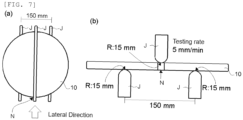
- FIG. 7 is a top view from the vertical direction
- FIG. 7 (b) is a side view.
- the breaking load of the notch portion of the bonded substrate 10 in Example 1 was 784 N, and the bending strength thereof was 245 Mpa.
- the breaking load of the notch portion of the bonded substrate in Comparative Example 1 was 732 N and the bending strength thereof was 228 Mpa. Consequently, it was found that the bonded substrate 10 in Example 1 had higher breaking strength than that of Comparative Example 1.
- a substrate for an electronic device was produced in the same way as in Example 1, except that a second silicon single-crystal substrate, being not nitrogen-doped unlike Example 1, was used (Example 2). As a result, GaN was successfully formed without generation of cracks and slips.
- a substrate for an electronic device was produced in the same way as in Comparative Example 1, except that a second silicon single-crystal substrate, not nitrogen-doped unlike Comparative Example 1, was used (Comparative Example 2). As a result, slip, etc., was not generated, but breaking strength was inferior compared with Example 2, as described later.
- Example 2 bonded substrates before forming nitride semiconductor films were produced, and the strength of each bonded substrate was measured.
- the measuring method was the same as in Example 1 and Comparative Example 1.
- the breaking load of the notch portion of the bonded substrate 10 in Example 2 was 713 N, and the bending strength thereof was 223 Mpa.
- the breaking load of the notch portion of the bonded substrate in Comparative Example 2 was 663 N and the bending strength thereof was 207 Mpa. Consequently, it was found that the bonded substrate 10 in Example 2 had higher breaking strength than that of Comparative Example 2.
- Example 1 in cases where nitrogen doping was present (Example 1 and Comparative Example 1), Example 1, in which the present invention was performed, exhibited more excellent results in the breaking load and the bending strength than Comparative Example 1. Moreover, even in cases where nitrogen doping was absent (Example 2 and Comparative Example 2), Example 2, in which the present invention was performed, exhibited more excellent results than Comparative Example 2.
- Comparative Example 1 exhibited better values than Example 2 but this is due to the difference between the presence and absence of nitrogen doping.
- conditions other than the off-angle such as the presence or absence of nitrogen doping
- the second silicon single-crystal substrate has the off-angle as in the present invention
- Substrates for an electronic device were produced in the same way as in Example 1, except that second silicon single-crystal substrates having off-angles of 2° (Example 3) and that of 8° (Example 4), unlike Example 1 were used.
- substrates for an electronic device were produced in the same way as in Example 2, except that second silicon single-crystal substrates having off-angles of 2° (Example 5) and that of 8° (Example 6) unlike Example 2, were used.
- GaN was successfully formed without generation of cracks or slips in each case.
- the breaking load and the bending strength of the notch portions of the bonded substrates 10 in Examples 3 to 6 were (753 N, 235 MPa), (803 N, 251 MPa), (697 N, 218 MPa), and (731 N, 228 MPa).
- Comparative Example 1 exhibited better values than or equivalent to Examples 5 and 6, this is because of the same reason when Comparative Example 1 was compared with Example 2, which is the difference between the presence and absence of nitrogen doping.
- the case where the second silicon single-crystal substrate has the off-angle as in the present invention, has higher breaking strength than the case where the off-angle is absent and can be utilized in suppressing the increase of warps or cracks.
Landscapes
- Chemical & Material Sciences (AREA)
- Engineering & Computer Science (AREA)
- Crystallography & Structural Chemistry (AREA)
- Materials Engineering (AREA)
- Metallurgy (AREA)
- Organic Chemistry (AREA)
- Chemical Kinetics & Catalysis (AREA)
- General Chemical & Material Sciences (AREA)
- Inorganic Chemistry (AREA)
- Recrystallisation Techniques (AREA)
Abstract
The present invention is a substrate for an electronic device, comprising a nitride semiconductor film formed on a bonded substrate comprising a silicon single crystal, wherein the bonded substrate is a substrate comprising a first silicon single-crystal substrate having a crystal plane orientation of {111} and a second silicon single-crystal substrate having a main surface that has an off-angle with respect to a crystal plane orientation of {100}, the first silicon single-crystal substrate and the second silicon single-crystal substrate being bonded via an oxide film, and
the nitride semiconductor film is formed on a surface of the first silicon single-crystal substrate of the bonded substrate. This provides a substrate for an electronic device, including a nitride semiconductor formed on a silicon single-crystal, which is the substrate for the electronic device with the suppressed generation of slips, cracks, etc., and with a high breaking strength, and provides a method for producing the substrate.
the nitride semiconductor film is formed on a surface of the first silicon single-crystal substrate of the bonded substrate. This provides a substrate for an electronic device, including a nitride semiconductor formed on a silicon single-crystal, which is the substrate for the electronic device with the suppressed generation of slips, cracks, etc., and with a high breaking strength, and provides a method for producing the substrate.
Description
- The present invention relates to a substrate for an electronic device and a method for producing the same, in particular, a substrate for an electronic device where a nitride semiconductor is formed on a silicon substrate and a method for producing the same.
- Nitride semiconductors, including GaN and AlN, can be used for fabricating high electron mobility transistors (HEMT) that uses two-dimensional electron gas and electronic devices with a high breakdown voltage.
- It is difficult to produce a nitride semiconductor wafer having a nitride semiconductor grown on a substrate, and a sapphire substrate or a SiC substrate is conventionally used as a growth substrate. However, in order to achieve a larger diameter substrate (diameter enlargement) and suppress costs for a substrate, epitaxial growth of a nitride semiconductor by vapor phase growth on a silicon single-crystal substrate has been employed. When an epitaxially grown film of the nitride semiconductor is produced by vapor phase growth on a silicon single-crystal substrate, a substrate with a larger diameter can be used compared to a sapphire substrate or a SiC substrate; thus, the productivity of devices is high and processing is easy, and therefore there are advantages. However, due to stress caused by a difference in lattice constant or a difference in thermal expansion coefficient, an increase in warps, slips, cracks, and the like easily occurs at the vapor phase growth of the nitride semiconductor on the silicon single-crystal substrate. Therefore, stress reduction is carried out through growth conditions and a relief layer.
- In particular, in order to make epitaxial substrates for power devices to have high breakdown voltage, it is necessary to produce GaN on Si (GaN on a silicon single-crystal) in which an epitaxial layer of GaN has increased thickness. To increase the thickness of the epitaxial layer, the silicon single-crystal substrate, being the growth substrate, may be thickened and epitaxial growth may be performed. In addition, as a method to thicken the silicon single-crystal substrate, bonding of two silicon single-crystal substrates has been conducted.
Patent Document 1 discloses the thickness of a bonded substrate of 2 mm or more. Moreover,Patent Document 2 discloses a combination of two substrates to be bonded, including a bond wafer having a plane orientation of {111} and a base wafer having a plane orientation of {100} and a resistivity of 0.1 Qcm or less. -
- Patent Document 1:
JP 2021-014376 A - Patent Document 2:
JP 2021-027186 A - As described above, the use of bonded substrates as growth substrates is known as disclosed in
Patent Document 1 andPatent Document 2. However, even if these bonded substrates are used, it has not been possible to completely suppress an increase in warps and generation of slips, cracks, and the like. Moreover, the slips, the cracks, and the like have often been generated mainly at a notch portion of the substrates. Generally, the notch is formed in <110> direction on the {111} silicon single-crystal substrate and formed in <110> direction or <100> direction on a {100} silicon single-crystal substrate. - The present invention has been made to solve the above-described problem. An object of the present invention is to provide a substrate for an electronic device, including a nitride semiconductor formed on a silicon single-crystal, which is the substrate for the electronic device with the suppressed generation of the slips, the cracks, etc., and with high breaking strength, and a method for producing the substrate.
- To solve the problem described above, the present invention provides a substrate for an electronic device, comprising a nitride semiconductor film formed on a bonded substrate comprising a silicon single crystal, wherein
- the bonded substrate is a substrate comprising a first silicon single-crystal substrate having a crystal plane orientation of {111} and a second silicon single-crystal substrate having a main surface that has an off-angle with respect to a crystal plane orientation of {100}, the first silicon single-crystal substrate and the second silicon single-crystal substrate being bonded via an oxide film, and
- the nitride semiconductor film is formed on a surface of the first silicon single-crystal substrate of the bonded substrate.
- With regard to the crystal plane orientation, a cleavage plane with respect to the main surface (a bonding surface with the first silicon single-crystal substrate) is nonvertical (the cleavage plane is tilted) by providing the off-angle as in the second silicon single-crystal substrate of the present invention, instead of a just-crystal-plane-orientation substrate without the off-angle like a conventional second silicon single-crystal substrate. In this way, the cleavage plane being tilted of just one second silicon single-crystal substrate can make the substrate for the electronic device with a high breaking strength, in which an increase in warps and generation of slips, cracks (hereinafter also referred to as cracks, etc.) are suppressed compared with a conventional substrate where the cleavage plane of the second silicon single-crystal substrate is also vertical to a bonding surface.
- In this case, the second silicon single-crystal substrate can be nitrogen-doped.
- Such a substrate serves as the substrate for the electronic device having higher breaking strength.
- In addition, it is possible that the first silicon single-crystal substrate is formed with a notch in <110> direction,
- the second silicon single-crystal substrate is formed with a notch in <110> direction, and
- the bonded substrate is a substrate bonded to align a notch position of the first silicon single-crystal substrate and a notch position of the second silicon single-crystal substrate.
- Such a substrate serves as the substrate for an electronic device, with further suppressed generation of the cracks, etc., and with high breaking strength, due to a positional relationship between the cleavage planes of the to-be-bonded first silicon single-crystal substrate and the to-be-bonded second silicon single-crystal substrate.
the bonded substrate can have a diameter of 300 mm or larger. - Thus, the substrate having the high breaking strength of the present invention is particularly effective for the substrate for the electronic device having a large diameter, such as a diameter of 300 mm or larger.
- Moreover, the present invention provides a method for producing a substrate for an electronic device by forming a nitride semiconductor film on a bonded substrate comprising a silicon single crystal, the method comprising the steps of:
- preparing a first silicon single-crystal substrate having a crystal plane orientation of {111}, and a second silicon single-crystal substrate having a main surface that has an off-angle with respect to a crystal plane orientation of {100};
- thermally oxidizing at least one of the first silicon single-crystal substrate and the second silicon single-crystal substrate to form an oxide film on a surface;
- producing the bonded substrate by laminating the first silicon single-crystal substrate and the second silicon single-crystal substrate via the oxide film and then heat treating to bond the first silicon single-crystal substrate and the second silicon single-crystal substrate; and
- epitaxially growing the nitride semiconductor film on a surface of the first silicon single-crystal substrate of the bonded substrate.
- According to such an inventive method for producing the substrate for an electronic device, the second silicon single-crystal substrate having the cleavage plane tilted to the bonding surface is included, and thus, the substrate for the electronic device with suppressed generation of the cracks, etc., and with high breaking strength can be produced.
- In this case, the second silicon single-crystal substrate to be prepared can be nitrogen-doped.
- In this way, the substrate for the electronic device having higher breaking strength can be produced.
- Moreover, it is possible that the first silicon single-crystal substrate to be prepared is formed with a notch in <110> direction,
- the second silicon single-crystal substrate to be prepared is formed with a notch in <110> direction, and
- the first silicon single-crystal substrate and the second silicon single-crystal substrate are laminated and bonded so as to align a notch position of the first silicon single-crystal substrate and a notch position of the second silicon single-crystal substrate.
- In such a way, it is possible to produce the substrate for the electronic device with further suppressed generation of the cracks, etc., and with high breaking strength due to a positional relationship between the cleavage planes of the to-be-bonded first silicon single-crystal substrate and the to-be-bonded second silicon single-crystal substrate.
- Moreover, the first silicon single-crystal substrate and the second silicon single-crystal substrate to be prepared can have diameters of 300 mm or larger.
- The substrate having a high breaking strength, such as the substrate for the electronic device produced by the inventive producing method, is particularly effective for producing the substrate for the electronic device having a large diameter, such as a diameter of 300 mm or larger.
- According to such an inventive substrate for the electronic device and the method for producing the same, since the second silicon single-crystal substrate has an off-angle and a cleavage plane tilted to the bonding surface, and thus, the substrate for the electronic device with the suppressed generation of the cracks, etc., and with high breaking strength can be provided.
-
-
FIG. 1 is a schematic cross-sectional view illustrating an example of a substrate for an electronic device according to the present invention. -
FIG. 2 is an explanatory view illustrating an example of a positional relationship between a cleavage plane in a first silicon single-crystal substrate and a cleavage plane in a second silicon single-crystal substrate. -
FIG. 3 is a schematic view illustrating an example of cleavage planes of a first silicon single-crystal substrate and a second silicon single-crystal substrate viewed from a main surface side. -
FIG. 4 is a schematic view illustrating another example of cleavage planes of a first silicon single-crystal substrate and a second silicon single-crystal substrate viewed from a main surface side. -
FIG. 5 is a flowchart illustrating a schematic of an example of a method for producing a substrate for an electronic device according to the present invention. -
FIG. 6 is a photograph of a state in which a bonded substrate is mounted in a wafer box after removing an oxide film in Example and Comparative Example. -
FIG. 7 is a schematic view illustrating a state of breaking load test and bending strength test. (a) View from above in a vertical direction. (b) View from side. - Hereinafter, the present invention is described in detail with referring to the drawings. However, the present invention is not limited thereto.
- As shown in
FIG. 1 , in the inventive substrate for anelectronic device 20, anitride semiconductor film 21 is formed on a silicon single-crystal bondedsubstrate 10. In the description of the present invention, the silicon single-crystal bondedsubstrate 10 is also referred to simply as "bonded substrate." In this case, the bondedsubstrate 10 is a substrate in which a first silicon single-crystal substrate 11 having a crystal plane orientation of {111} and a second silicon single-crystal substrate 12 having a main surface that has an off-angle with respect to a crystal plane orientation of {100} are bonded via anoxide film 13. As shown inFIG. 1 , thenitride semiconductor film 21 is formed on the first silicon single-crystal substrate 11. - Note that, in this description, a line above the number commonly used in the Miller index notation is substituted by a "-" in front of a number. That is, for example, the notation [1-10] is synonymous with:

- Miller index notations are used in the usual way. That is, {} means a general term for equivalent crystal plane orientations, and () means each direction of the crystal plane orientations. In addition, <> indicates a general term for equivalent crystal axis directions, and [] means each direction of crystal axis directions.
- As described above; in order to make epitaxial substrates for power devices have high breakdown voltage, it is necessary to produce a substrate for an electronic device formed with a thick nitride semiconductor film on a silicon single-crystal substrate (for example, GaN on Si in which an epitaxial layer of GaN has increased thickness). To increase the thickness of the epitaxial layer, the silicon single-crystal substrate may be thickened and epitaxial growth may be performed. In addition, as a method to thicken the silicon substrate, bonding of two silicon single-crystal substrates has been conducted; however, even if the bonded substrate is used, a complete suppression of the cracks, etc., has not been achieved.
- However, in the inventive substrate for the
electronic device 20, as described above, two silicon single-crystal substrates, the first and second silicon single-crystal substrates crystal substrate 12 among them, the main surface has the off-angle with respect to the crystal plane orientation of {100}, thus a cleavage plane is nonvertical with respect to a bonding surface with the first silicon single-crystal substrate. In this case, when compared with a conventional substrate using a just-crystal-plane-orientation substrate without the off-angle, the substrate for the electronic device can be made with suppressed generation of the crack, etc. (increased warps, or slips, cracks) and with high breaking strength. -
FIG. 2 shows an example of a positional relationship between the cleavage plane in the first silicon single-crystal substrate 11 and the cleavage plane in the second silicon single-crystal substrate 12. Note that although a case where these cleavage planes are in close positions with each other in a vertical direction to the main surface is described as an example here (that is, the positions are close in planar view), the present invention is not limited to such a positional relationship. Moreover, a case having the off-angle in the left-and-right direction on a paper is given as an example inFIG. 2 , the direction of the off-angle is not particularly limited in the present invention. That is, regardless of the positions of the cleavage planes between the first silicon single-crystal substrate 11 and the second silicon single-crystal substrate 12 in a planar view being close or distant from each other; moreover, regardless of the direction of the off-angle direction of the second silicon single-crystal substrate 12 (e.g., even the front-and-back direction on paper inFIG. 2 ), the above-described effect of preventing the cracks, etc., can be achieved. - In contrast, when both substrates are just-crystal-plane-orientation substrates without the off-angle; the cracks, etc., are prone to be generated.
- The size of the off-angle is not particularly limited but can be, for example, more than 0° and 12° or less, preferably from 2° to 8°, particularly 4°.
- Note that, in the present invention, each position of forming notch of the first silicon single-
crystal substrate 11 and the second silicon single-crystal substrate 12 is not particularly limited. - In an example described below, the first silicon single-
crystal substrate 11 is formed with the notch in <110> direction, and the second silicon single-crystal substrate 12 is formed with the notch in <110> direction. Moreover, the bondedsubstrate 10 is bonded so as to align the notch position of the first silicon single-crystal substrate 11 and the notch position of the second silicon single-crystal substrate 12. - In such a case, in addition to obtaining the above-mentioned off-angle effect (improvement of the breaking strength), the breaking strength can be further improved by the positional shift between the cleavage planes of the first silicon single-crystal substrate and the second silicon single-crystal substrate in the planar view.
- More specifically, a state of bonding of the first silicon single-
crystal substrate 11 and the second silicon single-crystal substrate 12, as described above, is described by referring toFIG. 3 , a drawing seen from the main surface (main front surface) side of each substrate. In this context, an example in which the substrate having the crystal plane orientation of {111} and the notch at <110> position is the first silicon single-crystal substrate 11 and the substrate having the crystal plane orientation of {100} and the notch at <110> position is the second silicon single-crystal substrate 12, is described. - In
FIG. 3 , the cleavage plane of the first silicon single-crystal substrate 11 is schematically shown by a dotted line, and the cleavage plane of the second silicon single-crystal substrate 12 is schematically shown by a dashed line, respectively. As shown inFIG. 1 , when the first silicon single-crystal substrate 11 and the second silicon single-crystal substrate 12 are laminated, it is found that cleavage planes in the vertical direction of the drawing are shifted. The cleavage planes in the lateral direction of the drawing are overlapped. However, as for the entire bondedsubstrate 10, the effect of the shift of the cleavage planes in the vertical direction of the drawing improves the substrate strength of the bondedsubstrate 10. As a result, even in the presence of thenitride semiconductor film 21 formed on a surface of the first silicon single-crystal substrate 11 of the bondedsubstrate 10, the substrate for theelectronic device 20 can be made with the further suppressed generation of the cracks, etc., and with high breaking strength. - Moreover, in the inventive substrate for the
electronic device 20, thenitride semiconductor film 21 is formed on the surface of the first silicon single-crystal substrate 11 having the crystal plane orientation of {111}, thus the excellentnitride semiconductor film 21 is formed. - In
FIG. 4 , an example of another bonded substrate is shown. InFIG. 4 , an example in which the substrate having the crystal plane orientation of {111} and the notch at <110> position is the first silicon single-crystal substrate and the substrate having the crystal plane orientation of {100} and the notch at <100> position is the second silicon single-crystal substrate, is described. In this case, although the crystal axis direction of the formed notch of the second silicon single-crystal substrate differs from the case inFIG. 3 , others are the same as inFIG. 3 . As can be seen inFIG. 4 , when the first silicon single-crystal substrate 11 and the second silicon single-crystal substrate 12 are laminated, the cleavage planes are all in close proximity to each other. Even in a case likeFIG. 4 , because two silicon single-crystal substrates with crystal plane orientations of {111} and {100}, respectively, are bonded, and the second silicon single-crystal substrate 12 has the above off-angle, thus the strength of the bonded substrate and the substrate for the electronic device is enhanced, but the case inFIG. 3 has more enhanced strength than the case inFIG. 4 . - In the inventive substrate for the
electronic device 20, the diameter of the bonded substrate 10 (and the substrate for the electronic device 20) can also be made as a large diameter of 300 mm or larger because of the high substrate strength as described above. Conventionally, the substrate having such a large diameter has a case where the substrate strength is insufficient, and the cracks, etc., are generated; however, the inventive substrate for the electronic device can be made with high breaking strength, which suppresses these factors. The upper limit of the diameter of the bonded substrate 10 (and the substrate for the electronic device 20) is not particularly limited but can be, for example, 450 mm or smaller. - When the diameter of the bonded substrate 10 (and the substrate for the electronic device 20) is 300 mm or larger, the diameters of the first silicon single-
crystal substrate 11 and the second silicon single-crystal substrate 12 are also 300 mm or larger. The respective thickness of the first silicon single-crystal substrate 11 and the second silicon single-crystal substrate 12 is not particularly limited but can be suitably used in accordance with standards. In particular, when the diameter is 300 mm, the thickness can be 775 um. Such a silicon single-crystal substrate is used as a general substrate for a device, is inexpensive, and can be used without particular problems. As the thickness of the first silicon single-crystal substrate 11 and the second silicon single-crystal substrate 12, the substrate having a thickness of 500 µm to 1500 um can be used, for example. - Moreover, the second silicon single-
crystal substrate 12 can be nitrogen-doped. The strength of the second silicon single-crystal substrate 12 is further enhanced by nitrogen doping, resulting in the substrate for theelectronic device 20 with even higher breaking strength. The concentration of nitrogen is not particularly limited but can be, for example, 5×10¹³ to 5×10¹⁵ atoms/cm3. - Hereinafter, a method for producing the inventive substrate for the
electronic device 20 described above is described referring toFIG. 5 . - Firstly, as shown in S11 of
FIG. 5 , a first silicon single-crystal substrate 11 and a second silicon single-crystal substrate 12 are prepared (Step S11). In this case, a silicon single-crystal substrate having a crystal plane orientation of {111} and a notch formed in <110> direction is prepared as the first silicon single-crystal substrate 11. In addition, a silicon single-crystal substrate having a main surface that has an off-angle with respect to a crystal plane orientation of {100}, and a notch formed in <110> direction is prepared as the second silicon single-crystal substrate 12. - Note that in preparing the second silicon single-
crystal substrate 12 having the off-angle described above, such a substrate can be obtained, for example, by producing a single ingot having a growth axis direction of <100> and slicing thereof at a desired off-angle. - In this case, the diameters of the first silicon single-crystal substrate to be prepared and the second silicon single-crystal substrate to be prepared can be 300 mm or larger.
- Moreover, as the second silicon single-crystal substrate, in particular, the substrate can be nitrogen-doped. A method for nitrogen doping is not particularly limited, but a known method can be used. For example, in producing a silicon single crystal by a CZ method, a silicon ingot, nitrogen-doped by using a silicon wafer having a nitrogen film and the like as raw material, can be produced and cut out. Naturally, the first silicon single-crystal substrate may also be nitrogen-doped.
- Moreover, the first silicon single-
crystal substrate 11 and the second silicon single-crystal substrate 12 are bonded to make a bondedsubstrate 20, which is one silicon single-crystal substrate, so the first silicon single-crystal substrate 11 can be referred to as a bond wafer, and the second silicon single-crystal substrate 12 can be referred to as a base wafer. - The respective thickness of the first silicon single-
crystal substrate 11 and the second silicon single-crystal substrate 12 is not particularly limited but can be suitably used in accordance with standards. Moreover, the respective resistivity and impurity concentration of the first silicon single-crystal substrate 11 and the second silicon single-crystal substrate 12 can be determined as appropriate. - Next, as shown in S12 of
FIG. 5 , at least one of the first silicon single-crystal substrate 11 and the second silicon single-crystal substrate 12 is thermally oxidized to form an oxide film on a surface (Step S12). The oxide film formed here is a film to be anoxide film 13, as shown inFIG. 1 after bonding of both silicon single-crystal substrates. The forming method of this oxide film is not particularly limited, but, for example, the oxide film having a thickness of about 100 nm can be formed on the surface of the substrate by an oxidation heat treatment. The thickness of the oxide film is not particularly limited but, for example, can be 10 nm or more and 1000 nm or less. The oxide film may be formed on each of two silicon single-crystal substrates, or the oxide film may be formed on any one of silicon single-crystal substrates. - Next, as shown in S13 of
FIG. 5 , the first silicon single-crystal substrate 11 and the second silicon single-crystal substrate 12 are bonded (Step S13). In this case, firstly, it is preferred that the first silicon single-crystal substrate 11 and the second silicon single-crystal substrate 12 are laminated so as to align a notch position the first silicon single-crystal substrate 11 and a notch position of the second silicon single-crystal substrate 12. In that case, both silicon single-crystal substrates are laminated via the oxide film formed in Step S12. By performing heat treatment in this state, the first silicon single-crystal substrate 11 and the second silicon single-crystal substrate 12 are bonded to produce the bonded substrate 10 (seeFIG. 1 ). - Conditions (atmosphere, temperature, time, and the like) for the heat treatment (bonding heat treatment) are not particularly limited as long as the first silicon single-
crystal substrate 11 and the second silicon single-crystal substrate 12 can be bonded. The temperature of the bonding heat treatment can be, for example, at 400°C or higher and 1200°C or lower in a nitrogen atmosphere for 1 to 12 hours. - After this bonding heat treatment, it is preferred to clean a surface of the bonded
substrate 10 before the epitaxial growth of a nitride semiconductor film described later. In particular, it is preferred to remove the oxide film generated on the surface of the bonded substrate 10 (in particular, the surface of the first silicon single-crystal substrate 11) by hydrofluoric acid spin cleaning, etc. - In this way, after the bonding of the first silicon single-
crystal substrate 11 and the second silicon single-crystal substrate 12 to produce the bondedsubstrate 10, the nitride semiconductor film 21 (seeFIG. 1 ) is epitaxially grown on the surface of the first silicon single-crystal substrate 11 of the bonded substrate 10 (Step S14), as shown in S14 ofFIG. 5 . Note that regarding the first silicon single-crystal substrate 11, double-side polishing may be performed before this bonding, or even if not double-side polished before bonding, the main surface to be grown can be single-sided polished after bonding and before epitaxial growth. Naturally, regarding the second silicon single-crystal substrate 12, the double-side polishing may also be performed. - As the
nitride semiconductor film 21, an AlN layer, a GaN layer, an AlGaN layer, and the like can be formed. Thisnitride semiconductor film 21 can be formed by a common method. Moreover, an intermediate layer (buffer layer) can be formed as appropriate. In this way, the substrate for theelectronic device 20 shown inFIG. 1 can be produced. - Hereinafter, the present invention will be more specifically described showing Examples and Comparative Examples. However, the present invention is not limited to Example described below.
- In accordance with the inventive method for producing a substrate for an electronic device shown in
FIG. 5 , a substrate for anelectronic device 20 shown inFIG. 1 was produced. - Firstly, as a first silicon single-
crystal substrate 11, a double-side polished silicon single-crystal substrate having a diameter of 300 mm, a thickness of 775 µm, a crystal plane orientation of {111}, p-type, and resistivity of 1 kS2cm with a notch formed in <110> direction was prepared; and as a second silicon single-crystal substrate 12, a double-side polished silicon single-crystal substrate having a diameter of 300 mm, a thickness of 775 µm, a crystal plane orientation of {100}, p-type, and resistivity of 30 Ωcm with a notch formed in <110> direction was prepared (Step S11). - This first silicon single-
crystal substrate 11 and second silicon single-crystal substrate 12 had cleavage planes, respectively, as shown inFIG. 3 as a schematic view. - Note that with regard to the crystal plane orientation, the first silicon single-
crystal substrate 11 had a just-crystal-plane-orientation without an off-angle, and the second silicon single-crystal substrate 12 had a crystal plane orientation with an off-angle (4°). The direction of the off-angle was set in the opposite direction to the notch (0 o'clock direction inFIG. 3 ). - Moreover, the first silicon single-
crystal substrate 11 was not nitrogen-doped, the second silicon single-crystal substrate 12 was nitrogen-doped, and nitrogen concentration was 5×10¹³ atoms/cm3. - These prepared two silicon single-crystal substrates were processed with oxidation heat treatment to form an oxide film having a thickness of 100 nm, respectively (Step S12).
- Next, two silicon single-crystal substrates were bonded with aligning the notch positions, and then bonding heat treatment at 500°C in a nitrogen atmosphere was performed to produce a bonded substrate 10 (Step S13). Subsequently, hydrofluoric acid spin cleaning was performed on the bonded
substrate 10 to remove the oxide film on the surface. Note thatFIG. 6 shows a state where the substrate, after removing the oxide film, was mounted in a wafer BOX. - Next, an AlN layer of 150 nm, an AlGaN layer of 160 nm, a superlattice structure with 25 alternating pairs of GaN layers and AlN layers being laminated, a GaN layer of 1000 nm, an AlGaN layer of 20 nm, and a GaN layer of 3 nm were epitaxially grown to a total thickness of 1.8 um on the surface of the first silicon single-
crystal substrate 11 of the bondedsubstrate 10 as a nitride semiconductor film 21 (Step S14). - As a result, GaN was successfully formed without the generation of cracks or slips. Consequently, the substrate for
electronic device 20 was produced. - As described below, a substrate for an electronic device was produced in the same way as in Example 1, except that a just-crystal-plane-orientation substrate without an off-angle unlike Example 1, was used as a second silicon single-crystal substrate.
- Firstly, as a first silicon single-crystal substrate, a double-side polished silicon single-crystal substrate having a diameter of 300 mm, a thickness of 775 µm, a crystal plane orientation of {111}, p-type, and resistivity of 1 kΩcm with a notch formed in <110> direction was prepared; and as a second silicon single-crystal substrate, a double-side polished silicon single-crystal substrate having a diameter of 300 mm, a thickness of 775 µm, a crystal plane orientation of {100}, p-type, and resistivity of 30 Qcm with a notch formed in <110> direction was prepared.
- This first silicon single-crystal substrate and second silicon single-crystal substrate had cleavage planes, respectively, as shown in
FIG. 3 as a schematic view. - Note that with regard to the crystal plane orientation, not only the first silicon single-crystal substrate but also the second silicon single-crystal substrate had a just-crystal-plane-orientation without an off-angle.
- Moreover, the first silicon single-crystal substrate was not nitrogen-doped, the second silicon single-crystal substrate was nitrogen-doped, and nitrogen concentration was 5×10¹³ atoms/cm3.
- These provided two silicon single-crystal substrates were processed with oxidation heat treatment to form an oxide film having a thickness of 100 nm, respectively.
- Next, two silicon single-crystal substrates were bonded with aligning the notch positions, and then bonding heat treatment at 500°C in a nitrogen atmosphere was performed to produce a bonded substrate. Note that this heat treatment process was performed simultaneously with the bonding heat treatment process in Example 1, as shown in
FIG. 6 . Subsequently, hydrofluoric acid spin cleaning was performed on the bondedsubstrate 10 to remove the oxide film on the surface. Note that the substrate, after removing the oxide film, was mounted in a wafer BOX (seeFIG. 6 ). - Next, a GaN film was epitaxially grown as a nitride semiconductor film on a surface of the first silicon single-crystal substrate of the bonded substrate on the same condition as in Example 1.
- As a result, although slip, etc., was not generated, breaking strength was inferior to Example 1, as described later.
- Hereinafter, the bonded substrates before forming the nitride semiconductor films were produced on the same conditions as in each of Example 1 and Comparative Example 1, and the strength of each bonded substrate was measured.
- In this strength measurement of the bonded substrate, as shown in
FIG. 7 , breaking load and bending strength were investigated using a Universal Testing System manufactured by INSTRON Corporation.FIG. 7 (a) is a top view from the vertical direction, andFIG. 7 (b) is a side view. - As shown in
FIGs. 7 (a) and (b) , three fulcrum jigs J (curvature radius R of crimping points is 15 mm) were arranged above and below the bonded substrate. In the bonded substrate, the notch position was weak in terms of strength, thus, the notch position N was arranged to be just below the central fulcrum jig J (seeFIGS. 7 (a) and (b) ). The formula for the bending strength is as follows.
- P: Breaking load,

- W: Width 300 mm
- T: Thickness 1.55 mm
- As a result, the breaking load of the notch portion of the bonded
substrate 10 in Example 1 was 784 N, and the bending strength thereof was 245 Mpa. On the other hand, the breaking load of the notch portion of the bonded substrate in Comparative Example 1 was 732 N and the bending strength thereof was 228 Mpa. Consequently, it was found that the bondedsubstrate 10 in Example 1 had higher breaking strength than that of Comparative Example 1. - A substrate for an electronic device was produced in the same way as in Example 1, except that a second silicon single-crystal substrate, being not nitrogen-doped unlike Example 1, was used (Example 2). As a result, GaN was successfully formed without generation of cracks and slips.
- Moreover, a substrate for an electronic device was produced in the same way as in Comparative Example 1, except that a second silicon single-crystal substrate, not nitrogen-doped unlike Comparative Example 1, was used (Comparative Example 2). As a result, slip, etc., was not generated, but breaking strength was inferior compared with Example 2, as described later.
- In addition, based on the same conditions as in each of Example 2 and Comparative Example 2, bonded substrates before forming nitride semiconductor films were produced, and the strength of each bonded substrate was measured. The measuring method was the same as in Example 1 and Comparative Example 1.
- As a result, the breaking load of the notch portion of the bonded
substrate 10 in Example 2 was 713 N, and the bending strength thereof was 223 Mpa. On the other hand, the breaking load of the notch portion of the bonded substrate in Comparative Example 2 was 663 N and the bending strength thereof was 207 Mpa. Consequently, it was found that the bondedsubstrate 10 in Example 2 had higher breaking strength than that of Comparative Example 2. - The results of the above breaking load and bending strength are summarized in Table 1.
[Table 1] Nitrogen doping Off Breaking Load N Bending Strength MPa Example 1 Present 4° off 784 245 Comparative Example 1 Present just 732 228 Example 2 Absent 4° off 713 223 Comparative Example 2 Absent just 663 207 - As described above, or as can be seen from Table 1, in cases where nitrogen doping was present (Example 1 and Comparative Example 1), Example 1, in which the present invention was performed, exhibited more excellent results in the breaking load and the bending strength than Comparative Example 1. Moreover, even in cases where nitrogen doping was absent (Example 2 and Comparative Example 2), Example 2, in which the present invention was performed, exhibited more excellent results than Comparative Example 2.
- Note that Comparative Example 1 exhibited better values than Example 2 but this is due to the difference between the presence and absence of nitrogen doping. When conditions other than the off-angle, such as the presence or absence of nitrogen doping, are the same condition, and when the second silicon single-crystal substrate has the off-angle as in the present invention, it is clear from the results described above that such a substrate is more excellent than a substrate without off-angle, in terms of the breaking load and the bending strength, and extremely effective in suppressing conventional problems such as increase of warps or cracks.
- Substrates for an electronic device were produced in the same way as in Example 1, except that second silicon single-crystal substrates having off-angles of 2° (Example 3) and that of 8° (Example 4), unlike Example 1 were used.
- Moreover, substrates for an electronic device were produced in the same way as in Example 2, except that second silicon single-crystal substrates having off-angles of 2° (Example 5) and that of 8° (Example 6) unlike Example 2, were used.
- As a result, GaN was successfully formed without generation of cracks or slips in each case.
- In addition, based on the same condition as in each of Examples 3 to 6, bonded substrates before forming nitride semiconductor films were produced, and the strength of each bonded substrate was measured. The measuring method was the same as in Example 1.
- As a result, the breaking load and the bending strength of the notch portions of the bonded
substrates 10 in Examples 3 to 6 were (753 N, 235 MPa), (803 N, 251 MPa), (697 N, 218 MPa), and (731 N, 228 MPa). - Consequently, it was found that the bonded
substrates 10 in Examples 3 and 4 had higher breaking strength than that of Comparative Example 1. Moreover, it was found that the bondedsubstrates 10 in Examples 5 and 6 had higher breaking strength than that of Comparative Example 2. - The results of the breaking load and bending strength in Examples 3 to 6 are summarized in Table 2.
[Table 2] Nitrogen doping Off Breaking Load N Bending Strength MPa Example 3 Present 2° off 753 235 Example 4 Present 8° off 803 251 Example 5 Absent 2° off 697 218 Example 6 Absent 8° off 731 228 - As described above, or as can be seen from Tables 1 and 2, in cases where nitrogen doping was present (Examples 3 and 4, and Comparative Example 1), Examples 3 and 4, in which the present invention was performed, exhibited more excellent results in the breaking load and the bending strength than Comparative Example 1. Moreover, even in cases where nitrogen doping was absent (Examples 5 and 6, and Comparative Example 2), Examples 5 and 6, in which the present invention was performed, exhibited more excellent results than Comparative Example 2.
- Furthermore, as can be seen from comparisons within Examples 1, 3, and 4 and comparisons within Examples 2, 5, and 6, the larger the off-angle, the better the breaking strength result.
- Note that although Comparative Example 1 exhibited better values than or equivalent to Examples 5 and 6, this is because of the same reason when Comparative Example 1 was compared with Example 2, which is the difference between the presence and absence of nitrogen doping. When conditions other than the off-angle are the same condition, the case where the second silicon single-crystal substrate has the off-angle, as in the present invention, has higher breaking strength than the case where the off-angle is absent and can be utilized in suppressing the increase of warps or cracks.
- This description encompasses the following aspects.
- [1]: A substrate for an electronic device, comprising a nitride semiconductor film formed on a bonded substrate comprising a silicon single crystal, wherein
- the bonded substrate is a substrate comprising a first silicon single-crystal substrate having a crystal plane orientation of {111} and a second silicon single-crystal substrate having a main surface that has an off-angle with respect to a crystal plane orientation of {100}, the first silicon single-crystal substrate and the second silicon single-crystal substrate being bonded via an oxide film, and
- the nitride semiconductor film is formed on a surface of the first silicon single-crystal substrate of the bonded substrate.
- [2]: The substrate for an electronic device according to [1] described above, wherein
the second silicon single-crystal substrate is nitrogen-doped. - [3]: The substrate for an electronic device according to [1] or [2] described above, wherein
- the first silicon single-crystal substrate is formed with a notch in <110> direction,
- the second silicon single-crystal substrate is formed with a notch in <110> direction, and
- the bonded substrate is a substrate bonded to align a notch position of the first silicon single-crystal substrate and a notch position of the second silicon single-crystal substrate.
- [4]: The substrate for an electronic device according to any one of [1] to [3] described above, wherein
the bonded substrate has a diameter of 300 mm or larger. - [5]: A method for producing a substrate for an electronic device by forming a nitride semiconductor film on a bonded substrate comprising a silicon single crystal, the method comprising the steps of:
- preparing a first silicon single-crystal substrate having a crystal plane orientation of {111}, and a second silicon single-crystal substrate having a main surface that has an off-angle with respect to a crystal plane orientation of {100};
- thermally oxidizing at least one of the first silicon single-crystal substrate and the second silicon single-crystal substrate to form an oxide film on a surface;
- producing the bonded substrate by laminating the first silicon single-crystal substrate and the second silicon single-crystal substrate via the oxide film and then heat treating to bond the first silicon single-crystal substrate and the second silicon single-crystal substrate; and
- epitaxially growing the nitride semiconductor film on a surface of the first silicon single-crystal substrate of the bonded substrate.
- [6]: The method for producing a substrate for an electronic device according to [5] described above, wherein
the second silicon single-crystal substrate to be prepared is nitrogen-doped. - [7]: The method for producing a substrate for an electronic device according to [5] or [6] described above, wherein
- the first silicon single-crystal substrate to be prepared is formed with a notch in <110> direction,
- the second silicon single-crystal substrate to be prepared is formed with a notch in <110> direction, and
- the first silicon single-crystal substrate and the second silicon single-crystal substrate are laminated and bonded so as to align a notch position of the first silicon single-crystal substrate and a notch position of the second silicon single-crystal substrate.
- [8]: The method for producing a substrate for an electronic device according to any one of [5] to [7] described above, wherein
the first silicon single-crystal substrate and the second silicon single-crystal substrate to be prepared have diameters of 300 mm or larger. - It should be noted that the present invention is not limited to the above-described embodiments. The embodiments are just examples, and any examples that have substantially the same feature and demonstrate the same functions and effects as those in the technical concept disclosed in claims of the present invention are included in the technical scope of the present invention.
Claims (10)
- A substrate for an electronic device, comprising a nitride semiconductor film formed on a bonded substrate comprising a silicon single crystal, whereinthe bonded substrate is a substrate comprising a first silicon single-crystal substrate having a crystal plane orientation of {111} and a second silicon single-crystal substrate having a main surface that has an off-angle with respect to a crystal plane orientation of {100}, the first silicon single-crystal substrate and the second silicon single-crystal substrate being bonded via an oxide film, andthe nitride semiconductor film is formed on a surface of the first silicon single-crystal substrate of the bonded substrate.
- The substrate for an electronic device according to claim 1, wherein
the second silicon single-crystal substrate is nitrogen-doped. - The substrate for an electronic device according to claim 1, whereinthe first silicon single-crystal substrate is formed with a notch in <110> direction,the second silicon single-crystal substrate is formed with a notch in <110> direction, andthe bonded substrate is a substrate bonded to align a notch position of the first silicon single-crystal substrate and a notch position of the second silicon single-crystal substrate.
- The substrate for an electronic device according to claim 2, whereinthe first silicon single-crystal substrate is formed with a notch in <110> direction,the second silicon single-crystal substrate is formed with a notch in <110> direction, andthe bonded substrate is a substrate bonded to align a notch position of the first silicon single-crystal substrate and a notch position of the second silicon single-crystal substrate.
- The substrate for an electronic device according to any one of claims 1 to 4, wherein
the bonded substrate has a diameter of 300 mm or larger. - A method for producing a substrate for an electronic device by forming a nitride semiconductor film on a bonded substrate comprising a silicon single crystal, the method comprising the steps of:preparing a first silicon single-crystal substrate having a crystal plane orientation of {111}, and a second silicon single-crystal substrate having a main surface that has an off-angle with respect to a crystal plane orientation of {100};thermally oxidizing at least one of the first silicon single-crystal substrate and the second silicon single-crystal substrate to form an oxide film on a surface;producing the bonded substrate by laminating the first silicon single-crystal substrate and the second silicon single-crystal substrate via the oxide film and then heat treating to bond the first silicon single-crystal substrate and the second silicon single-crystal substrate; andepitaxially growing the nitride semiconductor film on a surface of the first silicon single-crystal substrate of the bonded substrate.
- The method for producing a substrate for an electronic device according to claim 6, wherein
the second silicon single-crystal substrate to be prepared is nitrogen-doped. - The method for producing a substrate for an electronic device according to claim 6, whereinthe first silicon single-crystal substrate to be prepared is formed with a notch in <110> direction,the second silicon single-crystal substrate to be prepared is formed with a notch in <110> direction, andthe first silicon single-crystal substrate and the second silicon single-crystal substrate are laminated and bonded so as to align a notch position of the first silicon single-crystal substrate and a notch position of the second silicon single-crystal substrate.
- The method for producing a substrate for an electronic device according to claim 7, whereinthe first silicon single-crystal substrate to be prepared is formed with a notch in <110> direction,the second silicon single-crystal substrate to be prepared is formed with a notch in <110> direction, andthe first silicon single-crystal substrate and the second silicon single-crystal substrate are laminated and bonded so as to align a notch position of the first silicon single-crystal substrate and a notch position of the second silicon single-crystal substrate.
- The method for producing a substrate for an electronic device according to any one of claims 6 to 9, wherein
the first silicon single-crystal substrate and the second silicon single-crystal substrate to be prepared have diameters of 300 mm or larger.
Applications Claiming Priority (3)
| Application Number | Priority Date | Filing Date | Title |
|---|---|---|---|
| JP2022066618 | 2022-04-13 | ||
| JP2022153842A JP7694523B2 (en) | 2022-04-13 | 2022-09-27 | Substrate for electronic device and method for producing same |
| PCT/JP2023/006579 WO2023199616A1 (en) | 2022-04-13 | 2023-02-22 | Substrate for electronic devices and method for producing same |
Publications (1)
| Publication Number | Publication Date |
|---|---|
| EP4509645A1 true EP4509645A1 (en) | 2025-02-19 |
Family
ID=88329273
Family Applications (1)
| Application Number | Title | Priority Date | Filing Date |
|---|---|---|---|
| EP23788038.0A Pending EP4509645A1 (en) | 2022-04-13 | 2023-02-22 | Substrate for electronic devices and method for producing same |
Country Status (4)
| Country | Link |
|---|---|
| US (1) | US20250273587A1 (en) |
| EP (1) | EP4509645A1 (en) |
| TW (1) | TW202347764A (en) |
| WO (1) | WO2023199616A1 (en) |
Family Cites Families (5)
| Publication number | Priority date | Publication date | Assignee | Title |
|---|---|---|---|---|
| JPH09246505A (en) * | 1996-03-01 | 1997-09-19 | Hitachi Ltd | Semiconductor integrated circuit device |
| JP2009231376A (en) * | 2008-03-19 | 2009-10-08 | Shin Etsu Handotai Co Ltd | Soi wafer and semiconductor device, and method of manufacturing the soi wafer |
| JP7279552B2 (en) | 2019-07-11 | 2023-05-23 | 信越半導体株式会社 | Substrate for electronic device and manufacturing method thereof |
| JP6863423B2 (en) | 2019-08-06 | 2021-04-21 | 信越半導体株式会社 | Substrates for electronic devices and their manufacturing methods |
| JP7318580B2 (en) * | 2020-03-30 | 2023-08-01 | 信越半導体株式会社 | SOI wafer manufacturing method |
-
2023
- 2023-02-22 US US18/853,707 patent/US20250273587A1/en active Pending
- 2023-02-22 WO PCT/JP2023/006579 patent/WO2023199616A1/en not_active Ceased
- 2023-02-22 EP EP23788038.0A patent/EP4509645A1/en active Pending
- 2023-03-03 TW TW112107767A patent/TW202347764A/en unknown
Also Published As
| Publication number | Publication date |
|---|---|
| US20250273587A1 (en) | 2025-08-28 |
| TW202347764A (en) | 2023-12-01 |
| WO2023199616A1 (en) | 2023-10-19 |
Similar Documents
| Publication | Publication Date | Title |
|---|---|---|
| US11373863B2 (en) | Method of manufacturing a silicon carbide device and wafer composite including laser modified zones in a handle substrate | |
| US10600676B2 (en) | Group III nitride composite substrate and method for manufacturing the same, and method for manufacturing group III nitride semiconductor device | |
| JP4388741B2 (en) | Method for transferring semiconductor thin layer and method for manufacturing donor wafer used therefor | |
| EP4012750A1 (en) | Substrate for electronic device and production method therefor | |
| US11705330B2 (en) | Substrate for electronic device and method for producing the same | |
| WO2014125688A1 (en) | Group iii-nitride composite substrate and method of producing same, layered group iii-nitride composite substrate, as well as group iii-nitride semiconductor device and method of producing same | |
| JP7426642B2 (en) | Method for manufacturing silicon carbide epitaxial wafer | |
| CN105264644A (en) | Silicon-based substrate, semiconductor device, and semiconductor device manufacturing method | |
| JP2023165996A (en) | silicon carbide epitaxial wafer | |
| JP4633962B2 (en) | Manufacturing method of nitride semiconductor substrate | |
| JP2012066943A (en) | Substrate for forming nitride semiconductor, and nitride semiconductor | |
| US20250273587A1 (en) | Substrate for electronic device and method for producing the same | |
| JP7563434B2 (en) | Substrate for electronic device and method for producing same | |
| EP4442870A1 (en) | Substrate for electronic device and production method therefor | |
| EP4534740A1 (en) | Substrate for electronic device, and manufacturing method therefor | |
| JP7694523B2 (en) | Substrate for electronic device and method for producing same | |
| CN118215987A (en) | Nitride semiconductor substrate and method for manufacturing nitride semiconductor substrate | |
| JP5045095B2 (en) | Manufacturing method of semiconductor device | |
| CN118891405A (en) | Substrate for electronic device and method for manufacturing same | |
| JP7597081B2 (en) | Substrate for electronic device and method for producing same | |
| CN118414455A (en) | Substrate for electronic device and method for manufacturing the same | |
| WO2026100536A1 (en) | Epitaxial wafer and inspection method, capable of inspecting vertical element | |
| JP2026081618A (en) | Epitaxial wafer and inspection method capable of inspecting vertical elements | |
| CN118048691A (en) | Method for manufacturing laminated wafer and laminated wafer |
Legal Events
| Date | Code | Title | Description |
|---|---|---|---|
| STAA | Information on the status of an ep patent application or granted ep patent |
Free format text: STATUS: THE INTERNATIONAL PUBLICATION HAS BEEN MADE |
|
| PUAI | Public reference made under article 153(3) epc to a published international application that has entered the european phase |
Free format text: ORIGINAL CODE: 0009012 |
|
| STAA | Information on the status of an ep patent application or granted ep patent |
Free format text: STATUS: REQUEST FOR EXAMINATION WAS MADE |
|
| 17P | Request for examination filed |
Effective date: 20240919 |
|
| AK | Designated contracting states |
Kind code of ref document: A1 Designated state(s): AL AT BE BG CH CY CZ DE DK EE ES FI FR GB GR HR HU IE IS IT LI LT LU LV MC ME MK MT NL NO PL PT RO RS SE SI SK SM TR |
|
| DAV | Request for validation of the european patent (deleted) | ||
| DAX | Request for extension of the european patent (deleted) |