EP4503413A1 - Power converter and power conversion method capable of balancing energy and hybrid power supply - Google Patents
Power converter and power conversion method capable of balancing energy and hybrid power supply Download PDFInfo
- Publication number
- EP4503413A1 EP4503413A1 EP23198564.9A EP23198564A EP4503413A1 EP 4503413 A1 EP4503413 A1 EP 4503413A1 EP 23198564 A EP23198564 A EP 23198564A EP 4503413 A1 EP4503413 A1 EP 4503413A1
- Authority
- EP
- European Patent Office
- Prior art keywords
- switch
- capacitor
- inductor
- voltage
- output end
- Prior art date
- Legal status (The legal status is an assumption and is not a legal conclusion. Google has not performed a legal analysis and makes no representation as to the accuracy of the status listed.)
- Pending
Links
Images






Classifications
-
- H—ELECTRICITY
- H02—GENERATION; CONVERSION OR DISTRIBUTION OF ELECTRIC POWER
- H02M—APPARATUS FOR CONVERSION BETWEEN AC AND AC, BETWEEN AC AND DC, OR BETWEEN DC AND DC, AND FOR USE WITH MAINS OR SIMILAR POWER SUPPLY SYSTEMS; CONVERSION OF DC OR AC INPUT POWER INTO SURGE OUTPUT POWER; CONTROL OR REGULATION THEREOF
- H02M1/00—Details of apparatus for conversion
- H02M1/0095—Hybrid converter topologies, e.g. NPC mixed with flying capacitor, thyristor converter mixed with MMC or charge pump mixed with buck
-
- H—ELECTRICITY
- H02—GENERATION; CONVERSION OR DISTRIBUTION OF ELECTRIC POWER
- H02M—APPARATUS FOR CONVERSION BETWEEN AC AND AC, BETWEEN AC AND DC, OR BETWEEN DC AND DC, AND FOR USE WITH MAINS OR SIMILAR POWER SUPPLY SYSTEMS; CONVERSION OF DC OR AC INPUT POWER INTO SURGE OUTPUT POWER; CONTROL OR REGULATION THEREOF
- H02M3/00—Conversion of DC power input into DC power output
- H02M3/02—Conversion of DC power input into DC power output without intermediate conversion into AC
- H02M3/04—Conversion of DC power input into DC power output without intermediate conversion into AC by static converters
- H02M3/10—Conversion of DC power input into DC power output without intermediate conversion into AC by static converters using discharge tubes with control electrode or semiconductor devices with control electrode
- H02M3/145—Conversion of DC power input into DC power output without intermediate conversion into AC by static converters using discharge tubes with control electrode or semiconductor devices with control electrode using devices of a triode or transistor type requiring continuous application of a control signal
- H02M3/155—Conversion of DC power input into DC power output without intermediate conversion into AC by static converters using discharge tubes with control electrode or semiconductor devices with control electrode using devices of a triode or transistor type requiring continuous application of a control signal using semiconductor devices only
- H02M3/156—Conversion of DC power input into DC power output without intermediate conversion into AC by static converters using discharge tubes with control electrode or semiconductor devices with control electrode using devices of a triode or transistor type requiring continuous application of a control signal using semiconductor devices only with automatic control of output voltage or current, e.g. switching regulators
- H02M3/158—Conversion of DC power input into DC power output without intermediate conversion into AC by static converters using discharge tubes with control electrode or semiconductor devices with control electrode using devices of a triode or transistor type requiring continuous application of a control signal using semiconductor devices only with automatic control of output voltage or current, e.g. switching regulators including plural semiconductor devices as final control devices for a single load
-
- H—ELECTRICITY
- H02—GENERATION; CONVERSION OR DISTRIBUTION OF ELECTRIC POWER
- H02M—APPARATUS FOR CONVERSION BETWEEN AC AND AC, BETWEEN AC AND DC, OR BETWEEN DC AND DC, AND FOR USE WITH MAINS OR SIMILAR POWER SUPPLY SYSTEMS; CONVERSION OF DC OR AC INPUT POWER INTO SURGE OUTPUT POWER; CONTROL OR REGULATION THEREOF
- H02M3/00—Conversion of DC power input into DC power output
- H02M3/02—Conversion of DC power input into DC power output without intermediate conversion into AC
- H02M3/04—Conversion of DC power input into DC power output without intermediate conversion into AC by static converters
- H02M3/06—Conversion of DC power input into DC power output without intermediate conversion into AC by static converters using resistors or capacitors, e.g. potential divider
- H02M3/07—Conversion of DC power input into DC power output without intermediate conversion into AC by static converters using resistors or capacitors, e.g. potential divider using capacitors charged and discharged alternately by semiconductor devices with control electrode, e.g. charge pumps
-
- H—ELECTRICITY
- H02—GENERATION; CONVERSION OR DISTRIBUTION OF ELECTRIC POWER
- H02M—APPARATUS FOR CONVERSION BETWEEN AC AND AC, BETWEEN AC AND DC, OR BETWEEN DC AND DC, AND FOR USE WITH MAINS OR SIMILAR POWER SUPPLY SYSTEMS; CONVERSION OF DC OR AC INPUT POWER INTO SURGE OUTPUT POWER; CONTROL OR REGULATION THEREOF
- H02M1/00—Details of apparatus for conversion
- H02M1/0003—Details of control, feedback or regulation circuits
-
- H—ELECTRICITY
- H02—GENERATION; CONVERSION OR DISTRIBUTION OF ELECTRIC POWER
- H02M—APPARATUS FOR CONVERSION BETWEEN AC AND AC, BETWEEN AC AND DC, OR BETWEEN DC AND DC, AND FOR USE WITH MAINS OR SIMILAR POWER SUPPLY SYSTEMS; CONVERSION OF DC OR AC INPUT POWER INTO SURGE OUTPUT POWER; CONTROL OR REGULATION THEREOF
- H02M1/00—Details of apparatus for conversion
- H02M1/0067—Converter structures employing plural converter units, other than for parallel operation of the units on a single load
- H02M1/0077—Plural converter units whose outputs are connected in series
-
- H—ELECTRICITY
- H02—GENERATION; CONVERSION OR DISTRIBUTION OF ELECTRIC POWER
- H02M—APPARATUS FOR CONVERSION BETWEEN AC AND AC, BETWEEN AC AND DC, OR BETWEEN DC AND DC, AND FOR USE WITH MAINS OR SIMILAR POWER SUPPLY SYSTEMS; CONVERSION OF DC OR AC INPUT POWER INTO SURGE OUTPUT POWER; CONTROL OR REGULATION THEREOF
- H02M1/00—Details of apparatus for conversion
- H02M1/0083—Converters characterised by their input or output configuration
-
- H—ELECTRICITY
- H02—GENERATION; CONVERSION OR DISTRIBUTION OF ELECTRIC POWER
- H02M—APPARATUS FOR CONVERSION BETWEEN AC AND AC, BETWEEN AC AND DC, OR BETWEEN DC AND DC, AND FOR USE WITH MAINS OR SIMILAR POWER SUPPLY SYSTEMS; CONVERSION OF DC OR AC INPUT POWER INTO SURGE OUTPUT POWER; CONTROL OR REGULATION THEREOF
- H02M1/00—Details of apparatus for conversion
- H02M1/0083—Converters characterised by their input or output configuration
- H02M1/009—Converters characterised by their input or output configuration having two or more independently controlled outputs
-
- H—ELECTRICITY
- H02—GENERATION; CONVERSION OR DISTRIBUTION OF ELECTRIC POWER
- H02M—APPARATUS FOR CONVERSION BETWEEN AC AND AC, BETWEEN AC AND DC, OR BETWEEN DC AND DC, AND FOR USE WITH MAINS OR SIMILAR POWER SUPPLY SYSTEMS; CONVERSION OF DC OR AC INPUT POWER INTO SURGE OUTPUT POWER; CONTROL OR REGULATION THEREOF
- H02M1/00—Details of apparatus for conversion
- H02M1/0083—Converters characterised by their input or output configuration
- H02M1/0093—Converters characterised by their input or output configuration wherein the output is created by adding a regulated voltage to or subtracting it from an unregulated input
-
- H—ELECTRICITY
- H02—GENERATION; CONVERSION OR DISTRIBUTION OF ELECTRIC POWER
- H02M—APPARATUS FOR CONVERSION BETWEEN AC AND AC, BETWEEN AC AND DC, OR BETWEEN DC AND DC, AND FOR USE WITH MAINS OR SIMILAR POWER SUPPLY SYSTEMS; CONVERSION OF DC OR AC INPUT POWER INTO SURGE OUTPUT POWER; CONTROL OR REGULATION THEREOF
- H02M5/00—Conversion of AC power input into AC power output, e.g. for change of voltage, for change of frequency, for change of number of phases
- H02M5/02—Conversion of AC power input into AC power output, e.g. for change of voltage, for change of frequency, for change of number of phases without intermediate conversion into DC
- H02M5/04—Conversion of AC power input into AC power output, e.g. for change of voltage, for change of frequency, for change of number of phases without intermediate conversion into DC by static converters
- H02M5/22—Conversion of AC power input into AC power output, e.g. for change of voltage, for change of frequency, for change of number of phases without intermediate conversion into DC by static converters using discharge tubes with control electrode or semiconductor devices with control electrode
- H02M5/275—Conversion of AC power input into AC power output, e.g. for change of voltage, for change of frequency, for change of number of phases without intermediate conversion into DC by static converters using discharge tubes with control electrode or semiconductor devices with control electrode using devices of a triode or transistor type requiring continuous application of a control signal
- H02M5/293—Conversion of AC power input into AC power output, e.g. for change of voltage, for change of frequency, for change of number of phases without intermediate conversion into DC by static converters using discharge tubes with control electrode or semiconductor devices with control electrode using devices of a triode or transistor type requiring continuous application of a control signal using semiconductor devices only
- H02M5/2932—Conversion of AC power input into AC power output, e.g. for change of voltage, for change of frequency, for change of number of phases without intermediate conversion into DC by static converters using discharge tubes with control electrode or semiconductor devices with control electrode using devices of a triode or transistor type requiring continuous application of a control signal using semiconductor devices only with automatic control of output voltage, current or power
-
- H—ELECTRICITY
- H02—GENERATION; CONVERSION OR DISTRIBUTION OF ELECTRIC POWER
- H02M—APPARATUS FOR CONVERSION BETWEEN AC AND AC, BETWEEN AC AND DC, OR BETWEEN DC AND DC, AND FOR USE WITH MAINS OR SIMILAR POWER SUPPLY SYSTEMS; CONVERSION OF DC OR AC INPUT POWER INTO SURGE OUTPUT POWER; CONTROL OR REGULATION THEREOF
- H02M7/00—Conversion of AC power input into DC power output; Conversion of DC power input into AC power output
- H02M7/42—Conversion of DC power input into AC power output without possibility of reversal
- H02M7/44—Conversion of DC power input into AC power output without possibility of reversal by static converters
- H02M7/48—Conversion of DC power input into AC power output without possibility of reversal by static converters using discharge tubes with control electrode or semiconductor devices with control electrode
- H02M7/483—Converters with outputs that each can have more than two voltages levels
- H02M7/4833—Capacitor voltage balancing
Definitions
- the present disclosure relates to an energy balancing circuit and a method of adjusting capacitor voltages, and more particularly to a power converter with multiple output capacitors and a method of adjusting capacitor voltages.
- non-isolated power converters such as bidirectional power converters and single-to-multiple power converters
- the power converter can provide a single power supply to multiple loads, or transfer the power from one load to another load so as to achieve the purpose of energy balance and hybrid power supply.
- the design goals of the power converter include at least: 1. high conversion efficiency; 2. ability to withstand high current; 3. low input current ripple; 4. small size and low cost. Therefore, how to design the single-to-multiple power converter that is suitable for the above occasions and meets the design goals has become a critical topic in this field.
- An objective of the present disclosure is to provide a power converter.
- the power converter is coupled between a power source and multiple loads.
- the power converter includes a first switch module.
- the first switch module includes an inductor, a first switch, a second switch, a third switch, and a fourth switch.
- the inductor includes a first end and a second end.
- the first switch includes a first end connected to a first input end, and a second end connected to the first end of the inductor.
- the second switch incudes a first end connected to the second end of the inductor, and a second end connected to a second input end.
- the third switch includes a first end connected to a first output end, and a second end connected to the first end of the second switch and the second end of the inductor.
- the fourth switch includes a first end connected to the second end of the first switch and the first end of the inductor, and a second end connected to a second output end.
- the first switch, the second switch, the third switch, and the fourth switch are configured to be turned on or off, such that the inductor stores or releases energy to convert the power source into multiple voltages to the multiple loads.
- Another objective of the present disclosure is to provide a power conversion method.
- the method includes steps of: detecting multiple voltages of multiple loads to determine one of a first operation mode, a second operation mode, a third operation mode, a fourth operation mode, a fifth operation mode, and a sixth operation mode, and controlling the turn-on and turn-off of the first switch, the second switch, the third switch, and the fourth switch, such that the inductor stores or releases energy to respectively build a first voltage, a second voltage, and a third voltage to the multiple loads according to one of the six operation modes.
- the power converter and power conversion method proposed in the present disclosure have the following features and advantages: 1. by controlling the voltages of the capacitor units through duty cycle adjustment of the switches can reduce the number of components to achieve the advantages of small size and low cost; 2. through the energy storage and release of the inductor, and the control of multiple switches, the energy transfer between the voltages of the capacitor units can be controlled, and the voltages of the capacitor units can be adjusted to meet the requirements of different loads.
- FIG. 1 shows a circuit diagram of a power converter according to a first embodiment of the present disclosure.
- the power converter 10 is coupled between a power source 11 and multiple loads (including a first load 91, a second load 92, and a third load 93).
- the power converter 10 includes a first switch module 12.
- the first switch module 12 includes an inductor L 1 , a first switch S 1 , a second switch S 2 , a third switch S 3 , and a fourth switch S 4 .
- first load 91 is connected between a first input end IN1 and a first output end OUT1
- second load 92 is connected between the first output end OUT1 and a second output end OUT2
- third load 93 is connected between a second input end IN2 and the second output end OUT2.
- the first switch S 1 has a first end and a second end, in which the first end of the first switch S 1 is connected to the first input end IN1, and the second end of the first switch S 1 is connected to a first end of the inductor L 1 .
- the second switch S 2 has a first end and a second end, in which the first end of the second switch S 2 is connected to a second end of the inductor L 1 , and the second end of the second switch S 2 is connected to the second input end IN2.
- the third switch S 3 has a first end and a second end, in which the first end of the third switch S 3 is connected to the first output end OUT1, and the second end of the third switch S 3 is connected to the first end of the second switch S 2 and the second end of the inductor L 1 .
- the fourth switch S 4 has a first end and a second end, in which the first end of the fourth switch S 4 is connected to the second end of the first switch S 1 and the first end of the inductor L 1 , and the second end of the fourth switch S 4 is connected to the second output end OUT2.
- the first switch S 1 , the second switch S 2 , the third switch S 3 , and the fourth switch S 4 are configured to be turned on or off, such that the inductor L 1 stores or releases energy, so as to convert the power source 11 into multiple voltages to the multiple loads 91, 92, 93.
- the power converter 10 further includes a first capacitor C 1 , a second capacitor C 2 , and a third capacitor C 3 .
- the first capacitor C 1 is connected between the first input end IN1 and the first output end OUT1, and configured to build a first voltage V 1 .
- the second capacitor C 2 is connected between the first output end OUT1 and the second output end OUT2, and configured to build a second voltage V 2 .
- the third capacitor C 3 is connected between the second input end IN2 and the second output end OUT2, and configured to build a third voltage V 3 .
- the power source 11 is a DC (direct-current) power source, and connected between the first input end IN1 and the second input end IN2.
- the first switch S 1 , the second switch S 2 , the third switch S 3 , and the fourth switch S 4 are N-type synchronous rectification switches.
- the power converter 10 is controlled by a controller (not shown), such as a digital signal processor, a programmable logic controller, a microcontroller, and the like.
- the controller is configured to detect voltage change rates of the multiple loads (or capacitors) so as to determine that the power converter 10 executes one of the first to sixth operation modes. Specifically, when energy drop rate of one of the loads is significantly lower than that of the other loads, the energy stored in the load with the lowest energy drop rate needs to be transferred to the load with the highest energy drop rate. In other words, energy balance and hybrid power supply can be achieved by transferring the energy stored in the load with the least power consumption to the load with the most power consumption.
- the controller receives a user instruction to control the power converter 10 to execute which operation mode so as to realize energy scheduling.
- FIG. 2 shows a schematic diagram of the power converter in a first operation mode according to the present disclosure.
- the inductor L 1 stores energy stored in the first capacitor C 1 (as shown by a first energy-storing path Ps1), and a voltage across the inductor L 1 is the first voltage V 1 .
- the energy stored in the inductor L 1 releases to the second capacitor C 2 (as shown by a first energy-releasing path Pr1) to build the second voltage V 2 on the second capacitor C 2 .
- the condition for the power converter 10 to execute the first operation mode includes at least one of E 1 >E 3 >E 2 and E 1 >>E 2 , wherein E 1 , E 2 , and E 3 are respectively the energy stored in the first load 91, the second load 92, and the third load 93.
- the third switch S 3 may be replaced by a synchronous rectification switch or a diode.
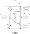
- FIG. 3 shows a schematic diagram of the power converter in a second operation mode according to the present disclosure.
- the inductor L 1 stores energy stored in the second capacitor C 2 (as shown by a second energy-storing path Ps2) to build the second voltage V 2 on the inductor L 1 .
- the energy stored in the inductor L 1 releases to the first capacitor C 1 (as shown by a second energy-releasing path Pr2) to build the first voltage V 1 on the first capacitor C 1 .
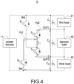
- FIG. 4 shows a schematic diagram of the power converter in a third operation mode according to the present disclosure.
- the inductor L 1 stores energy stored in the second capacitor C 2 (as shown by a third energy-storing path Ps3) to build the second voltage V 2 on the inductor L 1 .
- the energy stored in the inductor L 1 releases to the third capacitor C 3 (as shown by a third energy-releasing path Pr3) to build the third voltage V 3 on the third capacitor C 3 .
- FIG. 5 shows a schematic diagram of the power converter in a fourth operation mode according to the present disclosure.
- the inductor L 1 stores energy stored in the third capacitor C 3 (as shown by a fourth energy-storing path Ps4) to build the third voltage V 3 on the inductor L 1 .
- the energy stored in the inductor L 1 releases to the second capacitor C 2 (as shown by a fourth energy-releasing path Pr4) to build the second voltage V 2 on the second capacitor C 2 .
- FIG. 6 shows a schematic diagram of the power converter in a fifth operation mode according to the present disclosure.
- the inductor L 1 stores energy stored in the second capacitor C 2 (as shown by a fifth energy-storing path Ps5) to build the second voltage V 2 on the inductor L 1 .
- the energy stored in the inductor L 1 releases to the first capacitor C 1 , the second capacitor C 2 , and the third capacitor C 3 (as shown by a fifth energy-releasing path Pr5), to build the first voltage V 1 on the first capacitor C 1 , the second voltage V 2 on the second capacitor C 2 , and the third voltage V 3 on the third capacitor C 3 , and thus a voltage of V 1 +V 2 +V 3 is built on a series path formed by the three capacitors.
- energy can be transferred from the second capacitor C 2 to the first capacitor C 1 and the third capacitor C 3 , and the voltages of the first capacitor C 1 and the third capacitor C 3 can be stabilized.
- the condition for the power converter 10 to execute the fifth operation mode includes at least one of E 2 >E1 ⁇ E 3 and E 2 >>E 1 ⁇ E 3 .
- the fifth energy-releasing path Pr5 passes through a body diode of the first switch S 1 and a body diode of the second switch S 2 , the first switch S 1 and the second switch S 2 may be replaced by a synchronous rectification switch or a diode.
- FIG. 7 shows a schematic diagram of the power converter in a sixth operation mode according to the present disclosure.
- the inductor L 1 stores energy stored in the first capacitor C 1 , the second capacitor C 2 , and the third capacitor C 3 (as shown by a sixth energy-storing path Ps6) to build a voltage of V 1 +V 2 +V 3 on the inductor L 1 is a voltage of V 1 +V 2 +V.
- the energy stored in the inductor L 1 releases to the second capacitor C 2 (as shown by a sixth energy-releasing path Pr6) to build the second voltage V 2 on the second capacitor C 2 .
- energy can be transferred from the first capacitor C 1 , the second capacitor C 2 , and the third capacitor C 3 to the second capacitor C 2 , and the voltage of the second capacitor C 2 can be stabilized.
- the condition for the power converter 10 to execute the sixth operation mode includes at least one of E 2 ⁇ E1 ⁇ E 3 and E 2 ⁇ E 1 ⁇ E 3 .
- the third switch S 3 and the fourth switch S 4 may be replaced by a synchronous rectification switch or a diode.
- FIG. 8 shows a circuit diagram of the power converter 20 according to a second embodiment of the present disclosure.
- the former provides a multi-capacitor cascade structure.
- the multi-capacitor cascade structure includes a first capacitor string, a second capacitor string, and a third capacitor string.
- the first capacitor string includes multiple first capacitors C 11 , C 12 , connected between the first input end IN1 and the first output end OUT1, and configured to build a first voltage V 1 including multiple voltages V 11 , V 12 .
- the second capacitor string includes multiple second capacitors C 21 , C 22 , connected between the first output end OUT1 and the second output end OUT2, and configured to build a second voltage V 2 including multiple voltages V 21 , V 22 .
- the third capacitor string includes multiple third capacitors C 31 , C 32 , connected between the second input end IN2 and the second output end OUT2, and configured to build a third voltage V 3 including multiple voltages V 31 , V 32 .
- the power source 11 is a DC power source connected between the first input end IN1 and the second input end IN2.
- the first switch S 1 , the second switch S 2 , the third switch S 3 , and the fourth switch S 4 are N-type synchronous rectification switches.
- FIG. 9 shows a circuit diagram of the power converter 30 according to a third embodiment of the present disclosure.
- the power source 11 is an AC (alternating-current) power source
- the first switch S 1 , the second switch S 2 , the third switch S 3 , and the fourth switch S 4 are back-to-back bidirectional switches. Therefore, adapting to different positive and negative half cycles of the AC power source, the purpose of capacitor voltage adjustment can be achieved through the back-to-back bidirectional switch.
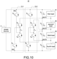
- a first end of the third switch S 3 of the second switch module 12-2 is connected to the second output end OUT2, and a second end of the fourth switch S 4 of the second switch module 12-2 is connected to the third output end OUT3.
- the fourth capacitor C 4 is connected between the third output end OUT3 and the second input end IN2, and configured to configured to build a fourth voltage V 4 .
- the fourth load 94 is connected between the third output end OUT3 and the second input end IN2.
- FIG. 11 shows a circuit diagram of the power converter 50 according to a fifth embodiment of the present disclosure.
- the power converter 50 is coupled between the power source 11 and multiple loads (including a first load 91, a second load 92, a third load 93, and a fourth load 94).
- the power converter 10 includes a first switch module 12-3.
- the first switch module 12-3 includes an inductor L 1 , a first switch S 1 , a second switch S 2 , a third switch S 3 , and a fourth switch S 4 .
- the first switch S 1 includes a first end connected to the first output end OUT1, and a second end connected to a first end of the inductor L 1 .
- the second switch S 2 includes a first end connected to a second end of the inductor L 1 , and a second end connected to the second input end IN2.
- Third switch S 3 includes a first end connected to the second output end OUT2, and a second end connected to the first end of the second switch S 2 and a second end of the inductor L 1 .
- the fourth switch S 4 includes a first end connected to the second end of the first switch S 1 and the first end of the inductor L 1 , and a second end connected to the third output end OUT3.
- the power converter 50 further includes a first capacitor C 1 , a second capacitor C 2 , and a third capacitor C 3 .
- the first capacitor C 1 is connected between the first input end IN1 and the first output end OUT1, and configured to build a first voltage V 1 .
- the second capacitor C 2 is connected between the first output end OUT1 and the second output end OUT2, and configured to build a second voltage V 2 .
- the third capacitor C 3 is connected between the second input end IN2 and the second output end OUT2, and configured to build a third voltage V 3 .
- the power source 11 is a DC power source, and connected between the first input end IN1 and the second input end IN2.
- the first switch S 1 , the second switch S 2 , the third switch S 3 , and the fourth switch S 4 are N-type synchronous rectification switches.
- the power converter 50 further includes a second switch module 12-4 and a fourth capacitor C 4 .
- the second switch module 12-4 includes a first switch S 1 , a second switch S 2 , a third switch S 3 , and a fourth switch S 4 .
- a first end of the first switch S 1 is connected to the first input end IN1
- a second end of the second switch S 2 is connected to the third output end OUT3
- a first end of the third switch S 3 is connected to the first output end OUT1
- a second end of the fourth switch S 4 is connected to the second output end OUT2.
- the fourth capacitor C 4 is connected between the third output end OUT3 and the second input end IN2.
- first load 91 is connected between the first input end IN1 and the first output end OUT1
- second load 92 is connected between the first output end OUT1 and the second output end OUT2
- third load 93 is connected between the second output end OUT2 and the third output end OUT3
- fourth load 94 is connected between the third output end OUT3 and the second input end IN2.
- the power source 11 is an AC power source
- the first switch S 1 , the second switch S 2 , the third switch S 3 , and the fourth switch S 4 are back-to-back bidirectional switches. Therefore, adapting to different positive and negative half cycles of the AC power source, the purpose of capacitor voltage adjustment can be achieved through the back-to-back bidirectional switch.
- FIG. 12 shows a circuit diagram of the power converter 60 according to a sixth embodiment of the present disclosure.
- One of the multiple loads is a first power source 51, and the first power source 51 is connected between the first input end IN1 and the first output end OUT1.
- One of the multiple loads is a second power source 52, and the second power source 52 is connected between the first output end OUT1 and the second output end OUT2.
- One of the multiple loads is a third power source 53, and the third power source 53 is connected between the second input end IN2 and the second output end OUT2.
- the power source 11 serves as a load 90 connected between the first input end IN1 and the second input end IN2.
- the first power source 51 and the first capacitor C 1 may be a battery, such as but not limited to a supercapacitor, a lithium battery, or a lead-acid battery.
- the second power source 52 and the second capacitor C 2 , and the third power source 53 and the third capacitor C 3 are both batteries. Therefore, the stable input voltage is provided by the battery, and the switches S 1 , S 2 , S 3 , S 4 of the first switch module 12 are controlled as described above so as to achieve a bidirectional power flow, stabilize the battery voltage for charging and discharging, and provide the demand for the power source 1 1(i.e., the load 90).
- FIG. 13 shows a flowchart of a power conversion method according to the present disclosure. The description will be made in conjunction with one of the embodiments of different power converters disclosed above.
- the power converter includes a first switch S 1 , a second switch S 2 , a third switch S 3 , a fourth switch S 4 , an inductor L 1 , a first capacitor C 1 , a second capacitor C 2 , and a third capacitor C 3 .
- the power conversion method includes steps as follows. First, detect multiple voltages of multiple loads to determine one of first to sixth operation modes (step S10).
- step S20 control the turn-on and turn-off of the first switch S 1 , the second switch S 2 , the third switch S 3 , and the fourth switch S 4 to make the inductor L 1 store or release energy to respectively build a first voltage V 1 , a second voltage V 2 , and a third voltage V 3 to multiple loads according to one of first to sixth operation modes.
- the method includes a step of: turning on the first switch S 1 so that the inductor L 1 stores energy stored in the first capacitor C 1 to build a first voltage V 1 on the inductor L 1 , and turning off the first switch S 1 so that the first voltage V 1 of the inductor L 1 releases energy to the second capacitor C 2 to build a second voltage V 2 on the second capacitor C2.
- the method includes a step of: turning on the third switch S 3 and the fourth switch S 4 so that the inductor L 1 stores energy stored in the second capacitor C 2 to build a second voltage V 2 on the inductor L 1 , and turning off the fourth switch S 4 and turning on the third switch S 3 so that the second voltage V 2 of the inductor L 1 releases energy to the first capacitor C 1 to build a first voltage V 1 on the first capacitor C 1 .
- the method includes a step of: turning on the third switch S 3 and the fourth switch S 4 so that the inductor L 1 stores energy stored in the second capacitor C 2 to build a second voltage V 2 on the inductor L 1 , and turning off the third switch S 3 and turning on the fourth switch S 4 so that the second voltage V 2 of the inductor L 1 releases energy to the third capacitor C 3 to build a third voltage V 3 on the third capacitor C 3 .
- the method includes a step of: turning on the second switch S 2 so that the inductor L 1 stores energy stored in the third capacitor C 3 to build a third voltage V 3 on the inductor L 1 , and turning off the second switch S 2 so that the third voltage V 3 of the inductor L 1 releases energy to the second capacitor C 2 to build a second voltage V 2 on the second capacitor C 2 .
- the method includes a step of: turning on the third switch S 3 and the fourth switch S 4 so that the inductor L 1 stores energy stored in the second capacitor C 2 to build a second voltage V 2 on the inductor L 1 , and turning off the third switch S 3 and the fourth switch S 4 so that the energy stored in the inductor L 1 releases to the first capacitor C 1 , the second capacitor C 2 , and the third capacitor C 3 to build a first voltage V 1 on the first capacitor C 1 , a second voltage V 2 on the second capacitor C 2 , and a third voltage V 3 on the third capacitor C 3 .
- the method includes a step of: turning on the first switch S 1 and the second switch S 2 so that the inductor L 1 stores energy stored in the first capacitor C 1 , the energy stored in the second capacitor C 2 , and the energy stored in the third capacitor C 3 to build a total voltage of V 1 +V 2 +V 3 (that is, the sum of the first voltage V 1 , the second voltage V 2 , and the third voltage V 3 ) on the inductor L 1 , and turning off the first switch S 1 or the second switch S 2 so that the total voltage of V 1 +V 2 +V 3 of the inductor L 1 releases energy to the second capacitor C 2 to build a second voltage V 2 on the second capacitor C 2 .
Landscapes
- Engineering & Computer Science (AREA)
- Power Engineering (AREA)
- Dc-Dc Converters (AREA)
Abstract
A power converter (10, 20, 30, 40, 50, 60) is coupled between a power source (11) and multiple loads (91, 92, 93, 94), and the power converter (10, 20, 30, 40, 50, 60) includes a first switch module (12, 12-1, 12-3). The switch module includes an inductor (L1), a first switch (S1), a second switch (S2), a third switch (S3), and a fourth switch (S4). The first switch (S1), the second switch (S2), the third switch (S3), and the fourth switch (S4) are configured to be turned on or turned off so that the inductor (L1) is stored energy or released energy to converter the power source (11) into multiple voltages to the multiple loads (91, 92, 93, 94).
Description
- The present disclosure relates to an energy balancing circuit and a method of adjusting capacitor voltages, and more particularly to a power converter with multiple output capacitors and a method of adjusting capacitor voltages.
- In recent years, non-isolated power converters, such as bidirectional power converters and single-to-multiple power converters, have been widely used in uninterruptible power systems, renewable energy systems, fuel cells, and hybrid vehicles. The power converter can provide a single power supply to multiple loads, or transfer the power from one load to another load so as to achieve the purpose of energy balance and hybrid power supply. In the above occasions, the design goals of the power converter include at least: 1. high conversion efficiency; 2. ability to withstand high current; 3. low input current ripple; 4. small size and low cost. Therefore, how to design the single-to-multiple power converter that is suitable for the above occasions and meets the design goals has become a critical topic in this field.
- An objective of the present disclosure is to provide a power converter. The power converter is coupled between a power source and multiple loads. The power converter includes a first switch module. The first switch module includes an inductor, a first switch, a second switch, a third switch, and a fourth switch. The inductor includes a first end and a second end. The first switch includes a first end connected to a first input end, and a second end connected to the first end of the inductor. The second switch incudes a first end connected to the second end of the inductor, and a second end connected to a second input end. The third switch includes a first end connected to a first output end, and a second end connected to the first end of the second switch and the second end of the inductor. The fourth switch includes a first end connected to the second end of the first switch and the first end of the inductor, and a second end connected to a second output end. The first switch, the second switch, the third switch, and the fourth switch are configured to be turned on or off, such that the inductor stores or releases energy to convert the power source into multiple voltages to the multiple loads.
- Another objective of the present disclosure is to provide a power conversion method. The method includes steps of: detecting multiple voltages of multiple loads to determine one of a first operation mode, a second operation mode, a third operation mode, a fourth operation mode, a fifth operation mode, and a sixth operation mode, and controlling the turn-on and turn-off of the first switch, the second switch, the third switch, and the fourth switch, such that the inductor stores or releases energy to respectively build a first voltage, a second voltage, and a third voltage to the multiple loads according to one of the six operation modes.
- Accordingly, the power converter and power conversion method proposed in the present disclosure have the following features and advantages: 1. by controlling the voltages of the capacitor units through duty cycle adjustment of the switches can reduce the number of components to achieve the advantages of small size and low cost; 2. through the energy storage and release of the inductor, and the control of multiple switches, the energy transfer between the voltages of the capacitor units can be controlled, and the voltages of the capacitor units can be adjusted to meet the requirements of different loads.
- It is to be understood that both the foregoing general description and the following detailed description are exemplary, and are intended to provide further explanation of the present disclosure as claimed. Other advantages and features of the present disclosure will be apparent from the following description, drawings, and claims.
- The present disclosure can be more fully understood by reading the following detailed description of the embodiment, with reference made to the accompanying drawing as follows:
-
FIG. 1 is a circuit diagram of a power converter according to a first embodiment of the present disclosure. -
FIG. 2 is a schematic diagram of the power converter in a first operation mode according to the present disclosure. -
FIG. 3 is a schematic diagram of the power converter in a second operation mode according to the present disclosure. -
FIG. 4 is a schematic diagram of the power converter in a third operation mode according to the present disclosure. -
FIG. 5 is a schematic diagram of the power converter in a fourth operation mode according to the present disclosure. -
FIG. 6 is a schematic diagram of the power converter in a fifth operation mode according to the present disclosure. -
FIG. 7 is a schematic diagram of the power converter in a sixth operation mode according to the present disclosure. -
FIG. 8 is a circuit diagram of the power converter according to a second embodiment of the present disclosure. -
FIG. 9 is a circuit diagram of the power converter according to a third embodiment of the present disclosure. -
FIG. 10 is a circuit diagram of the power converter according to a fourth embodiment of the present disclosure. -
FIG. 11 is a circuit diagram of the power converter according to a fifth embodiment of the present disclosure. -
FIG. 12 is a circuit diagram of the power converter according to a sixth embodiment of the present disclosure. -
FIG. 13 is a flowchart of a power conversion method according to the present disclosure. - Please refer to
FIG. 1 , which shows a circuit diagram of a power converter according to a first embodiment of the present disclosure. Thepower converter 10 is coupled between apower source 11 and multiple loads (including afirst load 91, asecond load 92, and a third load 93). Thepower converter 10 includes afirst switch module 12. As shown inFIG. 1 , thefirst switch module 12 includes an inductor L1, a first switch S1, a second switch S2, a third switch S3, and a fourth switch S4. In addition, thefirst load 91 is connected between a first input end IN1 and a first output end OUT1, thesecond load 92 is connected between the first output end OUT1 and a second output end OUT2, and thethird load 93 is connected between a second input end IN2 and the second output end OUT2. - The first switch S1 has a first end and a second end, in which the first end of the first switch S1 is connected to the first input end IN1, and the second end of the first switch S1 is connected to a first end of the inductor L1. The second switch S2 has a first end and a second end, in which the first end of the second switch S2 is connected to a second end of the inductor L1, and the second end of the second switch S2 is connected to the second input end IN2. The third switch S3 has a first end and a second end, in which the first end of the third switch S3 is connected to the first output end OUT1, and the second end of the third switch S3 is connected to the first end of the second switch S2 and the second end of the inductor L1. The fourth switch S4 has a first end and a second end, in which the first end of the fourth switch S4 is connected to the second end of the first switch S1 and the first end of the inductor L1, and the second end of the fourth switch S4 is connected to the second output end OUT2.
- In particular, the first switch S1, the second switch S2, the third switch S3, and the fourth switch S4 are configured to be turned on or off, such that the inductor L1 stores or releases energy, so as to convert the
power source 11 into multiple voltages to themultiple loads - As shown in
FIG. 1 , thepower converter 10 further includes a first capacitor C1, a second capacitor C2, and a third capacitor C3. The first capacitor C1 is connected between the first input end IN1 and the first output end OUT1, and configured to build a first voltage V1. The second capacitor C2 is connected between the first output end OUT1 and the second output end OUT2, and configured to build a second voltage V2. The third capacitor C3 is connected between the second input end IN2 and the second output end OUT2, and configured to build a third voltage V3. - In one embodiment, the
power source 11 is a DC (direct-current) power source, and connected between the first input end IN1 and the second input end IN2. The first switch S1, the second switch S2, the third switch S3, and the fourth switch S4 are N-type synchronous rectification switches. - In one embodiment, the
power converter 10 is controlled by a controller (not shown), such as a digital signal processor, a programmable logic controller, a microcontroller, and the like. The controller is configured to detect voltage change rates of the multiple loads (or capacitors) so as to determine that thepower converter 10 executes one of the first to sixth operation modes. Specifically, when energy drop rate of one of the loads is significantly lower than that of the other loads, the energy stored in the load with the lowest energy drop rate needs to be transferred to the load with the highest energy drop rate. In other words, energy balance and hybrid power supply can be achieved by transferring the energy stored in the load with the least power consumption to the load with the most power consumption. In other embodiments, the controller receives a user instruction to control thepower converter 10 to execute which operation mode so as to realize energy scheduling. - Please refer to
FIG. 2 , which shows a schematic diagram of the power converter in a first operation mode according to the present disclosure. As shown inFIG. 2 , based on the first switch S1 being turned on, the inductor L1 stores energy stored in the first capacitor C1 (as shown by a first energy-storing path Ps1), and a voltage across the inductor L1 is the first voltage V1. Based on the first switch S1 being turned off, the energy stored in the inductor L1 releases to the second capacitor C2 (as shown by a first energy-releasing path Pr1) to build the second voltage V2 on the second capacitor C2. In the first operation mode of the power converter, energy can be transferred from the first capacitor C1 to the second capacitor C2, and the voltage of the second capacitor C2 can be stabilized. In one embodiment, the condition for thepower converter 10 to execute the first operation mode includes at least one of E1>E3>E2 and E1>>E2, wherein E1, E2, and E3 are respectively the energy stored in thefirst load 91, thesecond load 92, and thethird load 93. In the first operation mode, since the first energy-storing path Ps1 and the first energy-releasing path Pr1 pass through a body diode of the third switch S3, the third switch S3 may be replaced by a synchronous rectification switch or a diode. - Please refer to
FIG. 3 , which shows a schematic diagram of the power converter in a second operation mode according to the present disclosure. As shown inFIG. 3 , based on the third switch S3 being turned on and the fourth switch S4 being turned on, the inductor L1 stores energy stored in the second capacitor C2 (as shown by a second energy-storing path Ps2) to build the second voltage V2 on the inductor L1. Based on the fourth switch S4 being turned off and the third switch S3 being still turned on, the energy stored in the inductor L1 releases to the first capacitor C1 (as shown by a second energy-releasing path Pr2) to build the first voltage V1 on the first capacitor C1. In the second operation mode of the power converter, energy can be transferred from the second capacitor C2 to the first capacitor C1, and the voltage of the first capacitor C1 can be stabilized. In one embodiment, the condition for thepower converter 10 to execute the second operation mode includes at least one of E2> E3>E1 and E2>>E1. In the second operation mode, since the second energy-releasing path Pr2 passes through a body diode of the first switch S1, the first switch S1 may be replaced by a synchronous rectification switch or a diode. - Please refer to
FIG. 4 , which shows a schematic diagram of the power converter in a third operation mode according to the present disclosure. As shown inFIG. 4 , based on the third switch S3 being turned on and the fourth switch S4 being turned on, the inductor L1 stores energy stored in the second capacitor C2 (as shown by a third energy-storing path Ps3) to build the second voltage V2 on the inductor L1. Based on the third switch S3 being turned off and the fourth switch S4 being still turned on, the energy stored in the inductor L1 releases to the third capacitor C3 (as shown by a third energy-releasing path Pr3) to build the third voltage V3 on the third capacitor C3. In the third operation mode of the power converter, energy can be transferred from the second capacitor C2 to the third capacitor C3, and the voltage of the third capacitor C3 can be stabilized. In one embodiment, the condition for thepower converter 10 to execute the third operation mode includes at least one of E2> E1>E3 and E2>>E3. In the third operation mode, since the third energy-releasing path Pr3 passes through a body diode of the second switch S2, the second switch S2 may be replaced by a synchronous rectification switch or a diode. - Please refer to
FIG. 5 , which shows a schematic diagram of the power converter in a fourth operation mode according to the present disclosure. As shown inFIG. 5 , based on the second switch S2 being turned on, the inductor L1 stores energy stored in the third capacitor C3 (as shown by a fourth energy-storing path Ps4) to build the third voltage V3 on the inductor L1. Based on the second switch S2 being turned off, the energy stored in the inductor L1 releases to the second capacitor C2 (as shown by a fourth energy-releasing path Pr4) to build the second voltage V2 on the second capacitor C2. In the fourth operation mode of the power converter, energy can be transferred from the third capacitor C3 to the second capacitor C2, and the voltage of the second capacitor C2 can be stabilized. In one embodiment, the condition for thepower converter 10 to execute the fourth operation mode includes at least one of E3> E1>E2 and E3>>E2. In the fourth operation mode, since the fourth energy-storing path Ps4 and the fourth energy-releasing path Pr4 pass through a body diode of the fourth switch S4, the fourth switch S4 may be replaced by a synchronous rectification switch or a diode. - Please refer to
FIG. 6 , which shows a schematic diagram of the power converter in a fifth operation mode according to the present disclosure. As shown inFIG. 6 , based on the third switch S3 being turned on and the fourth switch S4 being turned on, the inductor L1 stores energy stored in the second capacitor C2 (as shown by a fifth energy-storing path Ps5) to build the second voltage V2 on the inductor L1. Based on the third switch S3 being turned off and the fourth switch S4 being turned off, the energy stored in the inductor L1 releases to the first capacitor C1, the second capacitor C2, and the third capacitor C3 (as shown by a fifth energy-releasing path Pr5), to build the first voltage V1 on the first capacitor C1, the second voltage V2 on the second capacitor C2, and the third voltage V3 on the third capacitor C3, and thus a voltage of V1+V2+V3 is built on a series path formed by the three capacitors. In the fifth operation mode of the power converter, energy can be transferred from the second capacitor C2 to the first capacitor C1 and the third capacitor C3, and the voltages of the first capacitor C1 and the third capacitor C3 can be stabilized. In one embodiment, the condition for thepower converter 10 to execute the fifth operation mode includes at least one of E2>E1≒E3 and E2>>E1≒E3. In the fifth operation mode, since the fifth energy-releasing path Pr5 passes through a body diode of the first switch S1 and a body diode of the second switch S2, the first switch S1 and the second switch S2 may be replaced by a synchronous rectification switch or a diode. - Please refer to
FIG. 7 , which shows a schematic diagram of the power converter in a sixth operation mode according to the present disclosure. As shown inFIG. 7 , based on the first switch S1 being turned on and the second switch S2 being turned on, the inductor L1 stores energy stored in the first capacitor C1, the second capacitor C2, and the third capacitor C3 (as shown by a sixth energy-storing path Ps6) to build a voltage of V1+V2+V3 on the inductor L1 is a voltage of V1+V2+V. Based on the first switch S1 being turned off or the second switch S2 being turned off, the energy stored in the inductor L1 releases to the second capacitor C2 (as shown by a sixth energy-releasing path Pr6) to build the second voltage V2 on the second capacitor C2. In the sixth operation mode of the power converter, energy can be transferred from the first capacitor C1, the second capacitor C2, and the third capacitor C3 to the second capacitor C2, and the voltage of the second capacitor C2 can be stabilized. In one embodiment, the condition for thepower converter 10 to execute the sixth operation mode includes at least one of E2<E1≒E3 and E2<<E1≒E3. In the sixth operation mode, since the sixth energy-releasing path Pr6 passes through a body diode of the third switch S3 and a body diode of the fourth switch S4, the third switch S3 and the fourth switch S4 may be replaced by a synchronous rectification switch or a diode. - Please refer to
FIG. 8 , which shows a circuit diagram of thepower converter 20 according to a second embodiment of the present disclosure. A major difference between the second embodiment and the first embodiment shown inFIG. 1 is that the former provides a multi-capacitor cascade structure. In this embodiment, the multi-capacitor cascade structure includes a first capacitor string, a second capacitor string, and a third capacitor string. The first capacitor string includes multiple first capacitors C11, C12, connected between the first input end IN1 and the first output end OUT1, and configured to build a first voltage V1 including multiple voltages V11, V12. The second capacitor string includes multiple second capacitors C21, C22, connected between the first output end OUT1 and the second output end OUT2, and configured to build a second voltage V2 including multiple voltages V21, V22. The third capacitor string includes multiple third capacitors C31, C32, connected between the second input end IN2 and the second output end OUT2, and configured to build a third voltage V3 including multiple voltages V31, V32. In this embodiment, thepower source 11 is a DC power source connected between the first input end IN1 and the second input end IN2. The first switch S1, the second switch S2, the third switch S3, and the fourth switch S4 are N-type synchronous rectification switches. - Please refer to
FIG. 9 , which shows a circuit diagram of thepower converter 30 according to a third embodiment of the present disclosure. In this embodiment, thepower source 11 is an AC (alternating-current) power source, and the first switch S1, the second switch S2, the third switch S3, and the fourth switch S4 are back-to-back bidirectional switches. Therefore, adapting to different positive and negative half cycles of the AC power source, the purpose of capacitor voltage adjustment can be achieved through the back-to-back bidirectional switch. - Please refer to
FIG. 10 , which shows a circuit diagram of thepower converter 40 according to a fourth embodiment of the present disclosure. A major difference between the fourth embodiment and the first embodiment shown inFIG. 1 is that the former provides two switch modules, that is, a first switch module 12-1 and a second switch module 12-2, and four capacitors C1, C2, C3, C4, that is, a fourth capacitor C4 is extra compared with the above-mentioned embodiments. In this embodiment, the first switch module 12-1 is corresponding to thefirst switch module 12 in the first embodiment. A first end of the third switch S3 of the second switch module 12-2 is connected to the second output end OUT2, and a second end of the fourth switch S4 of the second switch module 12-2 is connected to the third output end OUT3. The fourth capacitor C4 is connected between the third output end OUT3 and the second input end IN2, and configured to configured to build a fourth voltage V4. Thefourth load 94 is connected between the third output end OUT3 and the second input end IN2. - Please refer to
FIG. 11 , which shows a circuit diagram of thepower converter 50 according to a fifth embodiment of the present disclosure. Thepower converter 50 is coupled between thepower source 11 and multiple loads (including afirst load 91, asecond load 92, athird load 93, and a fourth load 94). Thepower converter 10 includes a first switch module 12-3. As shown inFIG. 11 , the first switch module 12-3 includes an inductor L1, a first switch S1, a second switch S2, a third switch S3, and a fourth switch S4. The first switch S1 includes a first end connected to the first output end OUT1, and a second end connected to a first end of the inductor L1. The second switch S2 includes a first end connected to a second end of the inductor L1, and a second end connected to the second input end IN2. Third switch S3 includes a first end connected to the second output end OUT2, and a second end connected to the first end of the second switch S2 and a second end of the inductor L1. The fourth switch S4 includes a first end connected to the second end of the first switch S1 and the first end of the inductor L1, and a second end connected to the third output end OUT3. - As shown in
FIG. 11 , thepower converter 50 further includes a first capacitor C1, a second capacitor C2, and a third capacitor C3. The first capacitor C1 is connected between the first input end IN1 and the first output end OUT1, and configured to build a first voltage V1. The second capacitor C2 is connected between the first output end OUT1 and the second output end OUT2, and configured to build a second voltage V2. The third capacitor C3 is connected between the second input end IN2 and the second output end OUT2, and configured to build a third voltage V3. In this embodiment, thepower source 11 is a DC power source, and connected between the first input end IN1 and the second input end IN2. The first switch S1, the second switch S2, the third switch S3, and the fourth switch S4 are N-type synchronous rectification switches. - As shown in
FIG. 11 , thepower converter 50 further includes a second switch module 12-4 and a fourth capacitor C4. The second switch module 12-4 includes a first switch S1, a second switch S2, a third switch S3, and a fourth switch S4. A first end of the first switch S1 is connected to the first input end IN1, a second end of the second switch S2 is connected to the third output end OUT3, a first end of the third switch S3 is connected to the first output end OUT1, and a second end of the fourth switch S4 is connected to the second output end OUT2. The fourth capacitor C4 is connected between the third output end OUT3 and the second input end IN2. - In addition, the
first load 91 is connected between the first input end IN1 and the first output end OUT1, thesecond load 92 is connected between the first output end OUT1 and the second output end OUT2, thethird load 93 is connected between the second output end OUT2 and the third output end OUT3, and thefourth load 94 is connected between the third output end OUT3 and the second input end IN2. - In another embodiment, the
power source 11 is an AC power source, and the first switch S1, the second switch S2, the third switch S3, and the fourth switch S4 are back-to-back bidirectional switches. Therefore, adapting to different positive and negative half cycles of the AC power source, the purpose of capacitor voltage adjustment can be achieved through the back-to-back bidirectional switch. - Please refer to
FIG. 12 , which shows a circuit diagram of thepower converter 60 according to a sixth embodiment of the present disclosure. In the embodiment, when multiple loads supply power to thepower source 11. One of the multiple loads is afirst power source 51, and thefirst power source 51 is connected between the first input end IN1 and the first output end OUT1. One of the multiple loads is asecond power source 52, and thesecond power source 52 is connected between the first output end OUT1 and the second output end OUT2. One of the multiple loads is athird power source 53, and thethird power source 53 is connected between the second input end IN2 and the second output end OUT2. In this embodiment, thepower source 11 serves as aload 90 connected between the first input end IN1 and the second input end IN2. In this embodiment, thefirst power source 51 and the first capacitor C1 may be a battery, such as but not limited to a supercapacitor, a lithium battery, or a lead-acid battery. Similarly, thesecond power source 52 and the second capacitor C2, and thethird power source 53 and the third capacitor C3 are both batteries. Therefore, the stable input voltage is provided by the battery, and the switches S1, S2, S3, S4 of thefirst switch module 12 are controlled as described above so as to achieve a bidirectional power flow, stabilize the battery voltage for charging and discharging, and provide the demand for thepower source 1 1(i.e., the load 90). - Please refer to
FIG. 13 , which shows a flowchart of a power conversion method according to the present disclosure. The description will be made in conjunction with one of the embodiments of different power converters disclosed above. The power converter includes a first switch S1, a second switch S2, a third switch S3, a fourth switch S4, an inductor L1, a first capacitor C1, a second capacitor C2, and a third capacitor C3. The power conversion method includes steps as follows. First, detect multiple voltages of multiple loads to determine one of first to sixth operation modes (step S10). Afterward, control the turn-on and turn-off of the first switch S1, the second switch S2, the third switch S3, and the fourth switch S4 to make the inductor L1 store or release energy to respectively build a first voltage V1, a second voltage V2, and a third voltage V3 to multiple loads according to one of first to sixth operation modes (step S20). - In the first operation mode, the method includes a step of: turning on the first switch S1 so that the inductor L1 stores energy stored in the first capacitor C1 to build a first voltage V1 on the inductor L1, and turning off the first switch S1 so that the first voltage V1 of the inductor L1 releases energy to the second capacitor C2 to build a second voltage V2 on the second capacitor C2.
- In the second operation mode, the method includes a step of: turning on the third switch S3 and the fourth switch S4 so that the inductor L1 stores energy stored in the second capacitor C2 to build a second voltage V2 on the inductor L1, and turning off the fourth switch S4 and turning on the third switch S3 so that the second voltage V2 of the inductor L1 releases energy to the first capacitor C1 to build a first voltage V1 on the first capacitor C1.
- In the third operation mode, the method includes a step of: turning on the third switch S3 and the fourth switch S4 so that the inductor L1 stores energy stored in the second capacitor C2 to build a second voltage V2 on the inductor L1, and turning off the third switch S3 and turning on the fourth switch S4 so that the second voltage V2 of the inductor L1 releases energy to the third capacitor C3 to build a third voltage V3 on the third capacitor C3.
- In the fourth operation mode, the method includes a step of: turning on the second switch S2 so that the inductor L1 stores energy stored in the third capacitor C3 to build a third voltage V3 on the inductor L1, and turning off the second switch S2 so that the third voltage V3 of the inductor L1 releases energy to the second capacitor C2 to build a second voltage V2 on the second capacitor C2.
- In the fifth operation mode, the method includes a step of: turning on the third switch S3 and the fourth switch S4 so that the inductor L1 stores energy stored in the second capacitor C2 to build a second voltage V2 on the inductor L1, and turning off the third switch S3 and the fourth switch S4 so that the energy stored in the inductor L1 releases to the first capacitor C1, the second capacitor C2, and the third capacitor C3 to build a first voltage V1 on the first capacitor C1, a second voltage V2 on the second capacitor C2, and a third voltage V3 on the third capacitor C3.
- In the sixth operation mode, the method includes a step of: turning on the first switch S1 and the second switch S2 so that the inductor L1 stores energy stored in the first capacitor C1, the energy stored in the second capacitor C2, and the energy stored in the third capacitor C3 to build a total voltage of V1+V2+V3 (that is, the sum of the first voltage V1, the second voltage V2, and the third voltage V3) on the inductor L1, and turning off the first switch S1 or the second switch S2 so that the total voltage of V1+V2+V3 of the inductor L1 releases energy to the second capacitor C2 to build a second voltage V2 on the second capacitor C2.
- In conclusion, the present disclosure has following features and advantages:
- 1. The power converter proposed in the present disclosure controls the voltages of the capacitor units through duty cycle adjustment of the switches to reduce the number of components and achieve the advantages of small size and low cost.
- 2. Through the energy storage and release of the inductor, and the control of multiple switches, the energy transfer between the voltages of the capacitor units can be controlled, and the voltages of the capacitor units can be adjusted to meet the requirements of different loads.
Claims (15)
- A power converter (10, 20, 30, 40, 50, 60), coupled between a power source (11) and multiple loads (91, 92, 93, 94), characterized in that the power converter (10, 20, 30, 40, 50, 60) comprising:a first switch module (12, 12-1, 12-3) comprising:an inductor (L1) comprising a first end and a second end;a first switch (S1) comprising a first end connected to a first input end (IN1), and a second end connected to the first end of the inductor (L1);a second switch (S2) comprising a first end connected to the second end of the inductor (L1), and a second end connected to a second input end (IN2);a third switch (S3) comprising a first end connected to a first output end (OUT1), and a second end connected to the first end of the second switch (S2) and the second end of the inductor (L1); anda fourth switch (S4) comprising a first end connected to the second end of the first switch (S1), and a second end connected to a second output end (OUT2),wherein the first switch (S1), the second switch (S2), the third switch (S3), and the fourth switch (S4) are configured to be turned on or turned off, such that the inductor (L1) stores or releases energy to convert the power source (11) into multiple voltages (V1, V2, V3, V4) to the multiple loads (91, 92, 93, 94).
- The power converter (10, 20, 30, 40, 50, 60) of claim 1, further comprising:a first capacitor string comprising multiple first capacitors (C1) connected in series, connected between the first input end (IN1) and the first output end (OUT1), and configured to build a first voltage (V1);a second capacitor string comprising multiple second capacitors (C2) connected in series, connected between the first output end (OUT1) and the second output end (OUT2), and configured to build a second voltage (V2); anda third capacitor string comprising multiple third capacitors (C3) connected in series, connected between the second input end (IN2) and the second output end (OUT2), and configured to build a third voltage (V3);wherein the power source (11) is a DC power source connected between the first input end (IN1) and the second input end (IN2); and the first switch (S1), the second switch (S2), the third switch (S3), and the fourth switch (S4) are N-type synchronous rectification switches.
- The power converter (10, 20, 30, 40, 50, 60) of claim 1, further comprising:a second switch module (12-2, 12-4), wherein a first end of a third switch (S3) of the second switch module (12-2, 12-4) is connected to the second output end (OUT2), and a second end of a fourth switch (S4) of the second switch module (12-2, 12-4) is connected to a third output end (OUT3); anda fourth capacitor (C4) connected between the third output end (OUT3) and the second input end (IN2), and configured to build a fourth voltage (V4);wherein a fourth load (94) of the multiple loads (91, 92, 93, 94) is connected between the third output end (OUT3) and the second input end (IN2).
- The power converter (10, 20, 30, 40, 50, 60) of claim 1, wherein, when the multiple loads (91, 92, 93, 94) supply power to the power source (11):one of the multiple loads (91, 92, 93, 94) serves as a first power source (51) connected between the first input end (IN1) and the first output end (OUT1);one of the multiple loads (91, 92, 93, 94) serves as a second power source (52) connected between the first output end (OUT1) and the second output end (OUT2);one of the multiple loads (91, 92, 93, 94) serves as a third power source (53) connected between the second input end (IN2) and the second output end (OUT2); andthe power source (11) serves as a load (91, 92, 93, 94) connected between the first input end (IN1) and the second input end (IN2).
- A power converter (10, 20, 30, 40, 50, 60), coupled between a power source (11) and multiple loads (91, 92, 93, 94), characterized in that the power converter (10, 20, 30, 40, 50, 60) comprising:
a first switch module (12, 12-1, 12-3) comprising:an inductor (L1) comprising a first end and a second end;a first input end (IN1);a first switch (S1) comprising a first end connected to a first output end (OUT1), and a second end connected to the first end of the inductor (L1);a second switch (S2) comprising a first end connected to the second end of the inductor (L1), and a second end connected to a second input end (IN2);a third switch (S3) comprising a first end connected to a second output end (OUT2), and a second end connected to the first end of the second switch (S2) and the second end of the inductor (L1); anda fourth switch (S4) comprising a first end connected to the second end of the first switch (S1) and the first end of the inductor (L1), and a second end connected to a third output end (OUT3). - The power converter (10, 20, 30, 40, 50, 60) of claim 1 or claim 5, further comprising:a first capacitor (C1) connected between the first input end (IN1) and the first output end (OUT1), and configured to build a first voltage (V1);a second capacitor (C2) connected between the first output end (OUT1) and the second output end (OUT2), and configured to build a second voltage (V2); anda third capacitor (C3) connected between the second input end (IN2) and the second output end (OUT2), and configured to build a third voltage (V3);wherein the power source (11) is a DC power source connected between the first input end (IN1) and the second input end (IN2);wherein a first load (91) of the multiple loads (91, 92, 93, 94) is connected between the first input end (IN1) and the first output end (OUT1), a second load (92) of the multiple loads (91, 92, 93, 94) is connected between the first output end (OUT1) and the second output end (OUT2), and a third load (93) of the multiple loads (91, 92, 93, 94) is connected between the second input end (IN2) and the second output end (OUT2);wherein the first switch (S1), the second switch (S2), the third switch (S3), and the fourth switch (S4) are N-type synchronous rectification switches.
- The power converter (10, 20, 30, 40, 50, 60) of claim 1 or claim 5, wherein the power source (11) is an AC power source; and the first switch (S1), the second switch (S2), the third switch (S3), and the fourth switch (S4) are back-to-back bidirectional switches.
- The power converter (10, 20, 30, 40, 50, 60) of claim 5, further comprising:a second switch module (12-2, 12-4), wherein a first end of a first switch (S1) of the second switch module (12-2, 12-4) is connected to the first output end (OUT1), a second end of a second switch (S2) of the second switch module (12-2, 12-4) is connected to the third output end (OUT3), a first end of a third switch (S3) of the second switch module (12-2, 12-4) is connected to the first output end (OUT1), and a second end of a fourth switch (S4) of the second switch module (12-2, 12-4) is connected to the second output end (OUT2);a fourth capacitor (C4) connected between the third output end (OUT3) and the second input end (IN2); anda fourth load (94) of the multiple loads (91, 92, 93, 94) is connected between the third output end (OUT3) and the second input end (IN2).
- A power conversion method, used for the power converter (10, 20, 30, 40, 50, 60) of claim 1 or claim 5, the power converter (10, 20, 30, 40, 50, 60) comprising a first switch (S1), a second switch (S2), a third switch (S3), a fourth switch (S4), an inductor (L1), a first capacitor (C1), a second capacitor (C2), and a third capacitor (C3), characterized in that the power conversion method comprising steps of:detecting multiple voltages (V1, V2, V3, V4) of multiple loads (91, 92, 93, 94) to determine one of a first operation mode, a second operation mode, a third operation mode, a fourth operation mode, a fifth operation mode, and a sixth operation mode; andcontrolling turn-on and turn-off of the first switch (S1), the second switch (S2), the third switch (S3), and the fourth switch (S4), such that the inductor (L1) stores or releases energy to respectively build a first voltage (V1), a second voltage (V2), and a third voltage (V3) to the multiple loads (91, 92, 93, 94) according to one of the six operation modes.
- The power conversion method of claim 9, wherein in the first operation mode, comprising steps of:turning on the first switch (S1), so that the inductor (L1) stores the energy stored in the first capacitor (C1) to build the first voltage (V1) on the inductor (L1); andturning off the first switch (S1), so that the first voltage (V1) of the inductor (L1) releases energy to the second capacitor (C2) to build the second voltage (V2) on the second capacitor (C2).
- The power conversion method of claim 9, wherein in the second operation mode, comprising steps of:turning on the third switch (S3) and the fourth switch (S4), so that the inductor (L1) stores the energy stored in the second capacitor (C2) to build the first voltage (V1) on the inductor (L1); andturning off the fourth switch (S4) and turning on the third switch (S3), so that the second voltage (V2) of the inductor (L1) releases energy to the first capacitor (C1) to build the first voltage (V1) on the first capacitor (C1).
- The power conversion method of claim 9, wherein in the third operation mode, comprising steps of:turning on the third switch (S3) and the fourth switch (S4), so that the inductor (L1) stores the energy stored in the second capacitor (C2) to build the second voltage (V2) on the inductor (L1); andturning off the third switch (S3) and turning on the fourth switch (S4), so that the second voltage (V2) of the inductor (L1) releases energy to the third capacitor (C3) to build the third voltage (V3) on the third capacitor (C3).
- The power conversion method of claim 9, wherein in the fourth operation mode, comprising steps of:turning on the second switch (S2), so that the inductor (L1) stores the energy stored in the third capacitor (C3) to build third voltage (V3) on the inductor (L1); andturning off the second switch (S2), so that the third voltage (V3) of the inductor (L1) releases energy to the second capacitor (C2) to build the second voltage (V2) on the second capacitor (C2).
- The power conversion method of claim 9, wherein in the fifth operation mode, comprising steps of:turning on the third switch (S3) and the fourth switch (S4), so that the inductor (L1) stores the energy stored in the second capacitor (C2) to build the second voltage (V2) on the inductor (L1); andturning off the third switch (S3) and the fourth switch (S4), so that the energy stored in the inductor (L1) releases to the first capacitor (C1), the second capacitor (C2), and the third capacitor (C3) to build the first voltage (V1) on the first capacitor (C1), the second voltage (V2) on the second capacitor (C2), and the third voltage (V3) on the third capacitor (C3).
- The power conversion method of claim 9, wherein in the sixth operation mode, comprising steps of:turning on the first switch (S1) and the second switch (S2), so that the inductor (L1) stores the energy stored in the first capacitor (C1), the energy stored in the second capacitor (C2), and the energy stored in the third capacitor (C3) to build a total voltage on the inductor (L1); andturning off the first switch (S1) and the second switch (S2), so that the inductor (L1) releases the total voltage to the second capacitor (C2) to build the second voltage (V2) on the second capacitor (C2).
Applications Claiming Priority (1)
| Application Number | Priority Date | Filing Date | Title |
|---|---|---|---|
| CN202310954928.2A CN119448756A (en) | 2023-08-01 | 2023-08-01 | Power converter and power conversion method capable of balancing energy and hybrid power supply |
Publications (1)
| Publication Number | Publication Date |
|---|---|
| EP4503413A1 true EP4503413A1 (en) | 2025-02-05 |
Family
ID=88097642
Family Applications (1)
| Application Number | Title | Priority Date | Filing Date |
|---|---|---|---|
| EP23198564.9A Pending EP4503413A1 (en) | 2023-08-01 | 2023-09-20 | Power converter and power conversion method capable of balancing energy and hybrid power supply |
Country Status (4)
| Country | Link |
|---|---|
| US (1) | US12614983B2 (en) |
| EP (1) | EP4503413A1 (en) |
| JP (1) | JP2025022766A (en) |
| CN (1) | CN119448756A (en) |
Citations (4)
| Publication number | Priority date | Publication date | Assignee | Title |
|---|---|---|---|---|
| CN102244477A (en) * | 2011-07-07 | 2011-11-16 | 西南交通大学 | Multi-level converter with DC (direct current) capacitor assisted voltage-sharing circuit |
| EP3783784A2 (en) * | 2019-08-23 | 2021-02-24 | Eaton Intelligent Power Limited | Balancing multilevel dc-dc converter apparatus |
| EP3905509A1 (en) * | 2019-06-14 | 2021-11-03 | Huawei Technologies Co., Ltd. | Off-line phase split device and inverter system |
| EP4071990A1 (en) * | 2019-12-24 | 2022-10-12 | Huawei Digital Power Technologies Co., Ltd. | Conversion circuit and related electronic device |
Family Cites Families (17)
| Publication number | Priority date | Publication date | Assignee | Title |
|---|---|---|---|---|
| JPH06103984B2 (en) * | 1989-08-23 | 1994-12-14 | 東洋電機製造株式会社 | Buck-boost chopper device |
| US6002603A (en) * | 1999-02-25 | 1999-12-14 | Elliott Energy Systems, Inc. | Balanced boost/buck DC to DC converter |
| EP1356581B1 (en) * | 2001-01-17 | 2014-05-21 | ST-Ericsson SA | A controlled multi-output dc/dc converter |
| JP2004022562A (en) * | 2002-06-12 | 2004-01-22 | Murata Mfg Co Ltd | Capacitor module |
| JP4432443B2 (en) | 2003-10-14 | 2010-03-17 | オンキヨー株式会社 | Switching power supply circuit |
| TWI514738B (en) * | 2011-07-07 | 2015-12-21 | Sitronix Technology Corp | Voltage converter |
| US9529375B2 (en) | 2012-02-28 | 2016-12-27 | Texas Instruments Deutschland Gmbh | Single inductor-multiple output DC-DC converter, method for operating the same and electronic device comprising the converter |
| KR101373566B1 (en) | 2012-04-16 | 2014-03-12 | 전북대학교산학협력단 | Hybrid energy storage system and method |
| KR102199331B1 (en) * | 2013-08-22 | 2021-01-06 | 엘지이노텍 주식회사 | Power supply device |
| CN104167918B (en) | 2014-06-30 | 2017-06-13 | 阳光电源股份有限公司 | A kind of DC dc converter of transformation ratio high |
| CN106451576B (en) | 2016-10-27 | 2019-04-12 | 西安交通大学 | A kind of control method of the electric power electric transformer of single-phase multi output |
| TWI659589B (en) | 2018-06-11 | 2019-05-11 | 盈正豫順電子股份有限公司 | High-performed multi-level charging device and method thereof |
| JP2022544983A (en) | 2019-08-19 | 2022-10-24 | シグニファイ ホールディング ビー ヴィ | A switching power converter for converting a DC supply voltage to multiple balanced DC output voltages |
| CN112600423A (en) | 2021-03-02 | 2021-04-02 | 四川华泰电气股份有限公司 | Capacitance balance control system and method of three-level battery charging and discharging converter |
| CN113114040B (en) | 2021-03-25 | 2022-06-24 | 北京交通大学 | High-gain forward-flyback laminated boost converter |
| CN113364294B (en) | 2021-07-15 | 2022-07-26 | 南通大学 | Low voltage stress and low input current ripple high gain converter and control method |
| CN115589146A (en) | 2022-09-21 | 2023-01-10 | 华为数字能源技术有限公司 | Voltage converter, control method, battery module, electronic device and charging cabinet |
-
2023
- 2023-08-01 CN CN202310954928.2A patent/CN119448756A/en active Pending
- 2023-09-20 US US18/470,950 patent/US12614983B2/en active Active
- 2023-09-20 EP EP23198564.9A patent/EP4503413A1/en active Pending
-
2024
- 2024-07-02 JP JP2024106701A patent/JP2025022766A/en active Pending
Patent Citations (4)
| Publication number | Priority date | Publication date | Assignee | Title |
|---|---|---|---|---|
| CN102244477A (en) * | 2011-07-07 | 2011-11-16 | 西南交通大学 | Multi-level converter with DC (direct current) capacitor assisted voltage-sharing circuit |
| EP3905509A1 (en) * | 2019-06-14 | 2021-11-03 | Huawei Technologies Co., Ltd. | Off-line phase split device and inverter system |
| EP3783784A2 (en) * | 2019-08-23 | 2021-02-24 | Eaton Intelligent Power Limited | Balancing multilevel dc-dc converter apparatus |
| EP4071990A1 (en) * | 2019-12-24 | 2022-10-12 | Huawei Digital Power Technologies Co., Ltd. | Conversion circuit and related electronic device |
Also Published As
| Publication number | Publication date |
|---|---|
| JP2025022766A (en) | 2025-02-14 |
| CN119448756A (en) | 2025-02-14 |
| US12614983B2 (en) | 2026-04-28 |
| US20250047201A1 (en) | 2025-02-06 |
Similar Documents
| Publication | Publication Date | Title |
|---|---|---|
| CN102437609B (en) | Composite automatic synchronous energy transfer equalization circuit and equalization method for series battery pack | |
| US20150097546A1 (en) | Bidirectional dc-dc converter | |
| CN101599721B (en) | Solar power generation system and its control method | |
| US20240235213A9 (en) | Battery system and equalization management method therefor | |
| CN102655339A (en) | Power supply system | |
| CN102655346A (en) | Intelligent battery module and battery pack with automatic balance capability | |
| US11804730B2 (en) | Energy storage system and power supply method thereof | |
| Sarikhani et al. | A non-isolated buck-boost DC-DC converter with single switch | |
| CN114884116B (en) | Power supply circuit, new energy control system and energy coordination method | |
| US20210066928A1 (en) | Input voltage adapted power conversion | |
| CN113708442A (en) | Bypass type battery equalization device and control method | |
| Cheng et al. | Analysis of a three-port DC-DC converter for PV-battery system using DISO boost and SISO buck converters | |
| CN115843409B (en) | Power supply system, charging method, and discharging method | |
| CN113824310A (en) | Harvesting-managing single-stage fusion circuit for mechanical energy and its control method | |
| CN112803768A (en) | Three-port high-gain direct current converter | |
| JP2026508026A (en) | DC power converter for new energy generation, energy storage and microgrid bridging | |
| Moo et al. | Operation of battery power modules with series output | |
| US12614983B2 (en) | Power converter and power conversion method capable of balancing energy and hybrid power supply | |
| CN119010579A (en) | Single-inductor non-isolated three-port DC-DC converter and control method thereof | |
| TWI846555B (en) | Power converter and power conversion method capable of balancing energy and hybrid power supply | |
| CN117134464A (en) | Energy storage device, battery SOC equalization control method and computer-readable storage medium | |
| Zha et al. | Energy management system applied in DC electric springs | |
| CN115693732A (en) | A battery energy storage system and control method integrating PWM and transformer circuits | |
| WO2025025130A1 (en) | Power converter capable of energy balancing and hybrid power supply, and power conversion method | |
| RU133369U1 (en) | DEVICE FOR LEVELING THE VOLTAGE BALANCE OF THE BATTERY VOLTAGE (OPTIONS) |
Legal Events
| Date | Code | Title | Description |
|---|---|---|---|
| PUAI | Public reference made under article 153(3) epc to a published international application that has entered the european phase |
Free format text: ORIGINAL CODE: 0009012 |
|
| STAA | Information on the status of an ep patent application or granted ep patent |
Free format text: STATUS: THE APPLICATION HAS BEEN PUBLISHED |
|
| AK | Designated contracting states |
Kind code of ref document: A1 Designated state(s): AL AT BE BG CH CY CZ DE DK EE ES FI FR GB GR HR HU IE IS IT LI LT LU LV MC ME MK MT NL NO PL PT RO RS SE SI SK SM TR |
|
| STAA | Information on the status of an ep patent application or granted ep patent |
Free format text: STATUS: REQUEST FOR EXAMINATION WAS MADE |
|
| 17P | Request for examination filed |
Effective date: 20250805 |