EP4503035A1 - A 3d integrated charge coupled device memory - Google Patents
A 3d integrated charge coupled device memory Download PDFInfo
- Publication number
- EP4503035A1 EP4503035A1 EP23189157.3A EP23189157A EP4503035A1 EP 4503035 A1 EP4503035 A1 EP 4503035A1 EP 23189157 A EP23189157 A EP 23189157A EP 4503035 A1 EP4503035 A1 EP 4503035A1
- Authority
- EP
- European Patent Office
- Prior art keywords
- block
- ccd
- sub
- memory
- registers
- Prior art date
- Legal status (The legal status is an assumption and is not a legal conclusion. Google has not performed a legal analysis and makes no representation as to the accuracy of the status listed.)
- Granted
Links
Images




Classifications
-
- G—PHYSICS
- G11—INFORMATION STORAGE
- G11C—STATIC STORES
- G11C19/00—Digital stores in which the information is moved stepwise, e.g. shift registers
- G11C19/28—Digital stores in which the information is moved stepwise, e.g. shift registers using semiconductor elements
- G11C19/282—Digital stores in which the information is moved stepwise, e.g. shift registers using semiconductor elements with charge storage in a depletion layer, i.e. charge coupled devices [CCD]
-
- H—ELECTRICITY
- H10—SEMICONDUCTOR DEVICES; ELECTRIC SOLID-STATE DEVICES NOT OTHERWISE PROVIDED FOR
- H10D—INORGANIC ELECTRIC SEMICONDUCTOR DEVICES
- H10D84/00—Integrated devices formed in or on semiconductor substrates that comprise only semiconducting layers, e.g. on Si wafers or on GaAs-on-Si wafers
- H10D84/891—Integrated devices formed in or on semiconductor substrates that comprise only semiconducting layers, e.g. on Si wafers or on GaAs-on-Si wafers characterised by the integration of only components covered by H10D44/00, e.g. integration of charge-coupled devices [CCD] or charge injection devices [CID
Definitions
- the present disclosure relates to a charge-coupled device (CCD) memory.
- CCD charge-coupled device
- the disclosure provides an architecture and operation for a three-dimensional (3D) integrated CCD-based block-addressable storage class memory.
- SCM storage class memory
- PCM phase change memory
- MRAM magnetic random access memory
- cycling capability like low-latency NAND memory
- CCD-based block addressable SCM has emerged as a fundamentally new class of memory, and is considered a good candidate for bridging the memory gap, while having a significant cost advantage over DRAM.
- the CCDs lack the byte-addressability, which is conventionally required for RAM.
- One idea employed in this disclosure is to trade this byte-addressability for lower costs.
- a CCD-based memory array architecture is needed - along with efficient read, write, and refresh schemes - to realize the high memory cell densities desired.
- this disclosure aims to provide an improved SCM based on a CCD.
- An objective thereby is to provide a memory array architecture, which enables high memory cell densities.
- Another objective thereby is to provide a block-addressable SCM.
- Another objective is to provide, in particular, a write scheme for such a CCD-based SCM.
- the solutions of this disclosure are based on an integrated 3D memory array architecture, which - along with at least a corresponding write scheme - allows realizing a SCM with high memory cell density.
- a first aspect of this disclosure provides an integrated 3D CCD memory comprising: a layer stack including a plurality of gate layers and spacer layers, which are alternatingly arranged one on the other along a first direction; a plurality of semiconductor-based channels extending in the stack, wherein the channels form, in combination with the gate layers and one or more dielectric layers, a plurality of strings of charge storage capacitors operable as a plurality of CCD registers; a plurality of blocks, wherein each block comprises a plurality of sub-blocks, and wherein each sub-block comprises a set of the CCD registers; wherein each block and each sub-block of the block is individually selectable, in order to write information into at least one CCD register of the sub-block of the block.
- the charge storage capacitors may be connected in series to form the CCD registers.
- the charge storage capacitors may be MOS capacitors.
- the one or number of storage capacitors in the CCD register may be considered a memory cell of the CCD memory.
- the CCD memory of the first aspect can be used as SCM, under the premise that byte-addressability can be omitted.
- the CCD memory may provide high speeds, good reliability, nearly unlimited cycling, and low power consumption.
- the CCD memory of the first aspect is block-addressable, and even sub-block-addressable, which is beneficial for performance, endurance, and energy efficiency of the memory. Also the storage density can be increased.
- the 3D CCD memory further comprises a plurality of input transfer-gates, wherein each sub-block is associated with at least one input-transfer gate, and the at least one input transfer-gate is configured to select the sub-block.
- the plurality of input transfer-gates comprises a first set of input transfer-gates, which are associated with the sub-blocks of a first block, and a second set of input-transfer gates, which are associated with the sub-blocks of a second block.
- the input transfer-gate enable a controlled access of the memory, and are beneficial as they may isolate different sub-blocks of the memory. Thus, they may lead to a reduced power consumption of the memory.
- the input transfer-gates are defined in the topmost one or more gate layers of the layer stack, and wherein the topmost one or more gate layers are respectively separated into a plurality of parts, wherein each part is associated with one sub-block.
- the input transfer-gate-layers of the layer stack are cut, in order to separate the layers into the plurality of parts.
- the 3D CCD memory further comprises: a plurality of bit lines, wherein each bit line is associated with one or more CCD registers in a block and/or with one CCD register in a sub-block; and wherein the at least one input transfer-gate associated with the sub-block is operable to allow charge to be provided from a bit line to the CCD register associated with that bit line.
- bit lines associated with a block are connected to respective input junctions.
- the input junctions allow for an efficient charge transfer into the CCD registers.
- bit lines are further connected to a bit-line selector and driver circuit, which is configured to insert charge via the bit lines into the CCDs registers of the sub-block, it the at least one input-transfer gate associated with the sub-block is operated.
- the word lines may also be referred to as phase lines, and may be used to implement clocking. That is, the word lines may be used to coordinate the operation of a CCD register using a series of clocking phases, often referred to as PH1, PH2, etc. These clocking phases may be applied to different word lines, which may be used to control the potential barriers within the CCD register and thereby control the movement of charge along the CCD register.
- a second aspect of this disclosure provides a method of operating a 3D CCD memory of the first aspect or any of its implementations, wherein for writing information into a CCD register of one sub-block the method comprises: individually selecting a block and a sub-block in the block; and inserting charge into the CCD-registers included in the selected sub-block.
- selecting the sub-block comprises activating the at least one input-transfer gate, which is associated with the sub-block.
- inserting the charge into the CCD registers comprises changing a voltage on the input junction, to which the bit lines associated with the selected block are connected.
- the charge is inserted into the CCD registers of each block and is then moved simultaneously along the CCD registers by operating clocking phases associated with the charge storage capacitors in the CCD registers.
- the clocking phases may be operated by using and subsequently activating word lines that are associated with the clocking phases.
- the method of the second aspect achieves the same advantages as the 3D CCD memory of the first aspect, and may be extended by respective implementations as described above for the 3D CCD memory of the first aspect.
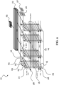
- FIG. 1 shows an integrated 3D CCD memory 10 according to this disclosure.
- the CCD memory 10 can be a block-addressable SCM.
- the CCD memory 10 may be used as a DRAM replacement in some of its use cases, or as an improved substitute for various other types of SCM.
- the CCD memory 10 of this disclosure may provide better scalability than a PCM, and/or may have a better power efficiency than a MRAM, and/or may have a better cycling capability than low-latency NAND memory.
- the CCD memory 10 comprises a layer stack 11, which includes a plurality of gate layers 11a and spacer layers 11b, which are alternatingly arranged one on the other along a first direction (which corresponds to the vertical direction in FIG. 1 ).
- the layer stack 11 may either start with a gate layer 11a or a spacer layer 11b (as bottommost layer), for instance, on a substrate.
- the layer stack 11 may likewise end with a gate layer 11a or a spacer layer 11b (as topmost layer), and the illustrated stack 11 of FIG. 1 is just an example.
- the CCD memory 10 further comprises a plurality of semiconductor-based channels 12 extending in the stack 11. These channels 12 form, in combination with the gate layers 11a and with one or more dielectric layers 13, which may respectively extend parallel and adjacent to the channels, a plurality of strings of charge storage capacitors. These charge storage capacitors are operable as a plurality of CCD registers 16. Notably, each gate layer 11a may surround one or more of the semiconductor-based channels 12.
- the semiconductor-based channels 12 may respectively be made of a semiconductor oxide material.
- the semiconductor oxide material may comprise at least one of indium gallium zinc oxide (IGZO), indium tin oxide (ITO), and indium zinc oxide (IZO), or another wide-bandgap oxide semiconductor.
- IGZO indium gallium zinc oxide
- ITO indium tin oxide
- IZO indium zinc oxide
- Such wide-bandgap oxide semiconductors allow achieving an increased retention time of the CCD memory 10.
- the semiconductor-based channels 12 may also be made of a silicon-based semiconductor material or of a III-V semiconductor material.
- a plurality of holes may formed through the entire layer stack 11, and may then be plugged with the semiconductor-based material, for example, with the semiconductor oxide material like IGZO, along with one or a plurality of the dielectric layers 13, wherein the dielectric layers 13 may each be arranged between one of the semiconductor-based channels and at least one of the gate layers 11a.
- the strings of charge storage capacitors connected together as a CCD register architecture are formed.
- FIG. 2 shows an architecture of an exemplary 3D CCD memory 10 of this disclosure, which builds on the CCD memory 10 shown in FIG. 1 . Accordingly, the architecture shown in FIG. 2 is also based on the 3D approach of the vertical CCD registers 16 with the horizontal gate layers 11a, as illustrated in FIG. 1 (where horizontal and vertical may denote two perpendicular directions).
- the CCD memory 10 also comprises a plurality of bit lines 24. Each bit line 24 is associated with one or more CCD registers 16 in a block 14 and/or is associated with one CCD register 16 in a sub-block 15.
- the CCD memory 10 further comprises a plurality of word lines 28, which may extend in the horizontal direction, as shown in FIG. 2 , or generally along a second direction, which is perpendicular to the first direction.
- the CCD registers 16 in one block 14 of the memory 10 are connected to the same set of word lines 28. These word lines 28 of the set are operable to allow charge to be transported along the CCD registers 16, for example, by using the word lines 28 to operate clocking phases associated with the charge storage capacitors in the CCD registers 16.
- Each CCD register 16 may comprises one or more output transfer-gates 29, which are defined in the one or more gate layers 11a that are closest to an output end of the CCD register 16. That is, the bottommost gate layers 11a in FIG. 1 may define the output transfer-gates 29 of the CCD register 16.
- the one or more output transfer-gates 29 may be controlled (e.g., by a subset of word lines 28) to allow charge to move from the string of charge storage capacitors of the CCD register 16 to an output of the CCD register 16, e.g., into a floating diffusion formed at the output end of the CCD register 16.
- the bit lines 24 can be connected to respective input junctions 25.
- the bit lines 24 may be further connected to a bit-line selector 26 and driver circuit 27, which are respectively configured to insert charge via the bit lines 24 into the CCDs registers 16 of the sub-block 15, if the at least one input-transfer gate 21, which is associated with the sub-block 15, is operated.
- a method 30 as shown in FIG. 3 may be performed.
- the method 30 comprises a step 31 of individually selecting a block 14 and a sub-block 15 in the block 14. That is, each sub-block 15 is individually addressable.
- the method 30 further comprises a step 32 of inserting charge into the CCD-registers 16 included in the selected sub-block 15.
- a variant of a "fill and-spill" procedure may be used to inject 32 the charge into at least one CCD register 16. This process of injecting 32 charge may be referred to as bit writing.
- the input transfer-gates 21 may thereby function to select a set of CCD registers 16 to do the write operation on them.
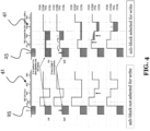
- FIG. 4 and FIG. 5 depict this bit writing scheme with one input-transfer gate 21 and with two input transfer-gates 21, respectively.
- the left side shows a sub-block 15 that is not selected for the write during the bit writing
- the right side shows the sub-block 15 that is selected for the write during the bit writing.
- the activation of at least one input-transfer gate 21, which is associated with the sub-block 15, results in the selection or addressing of that sub-block 15.
- the input transfer-gate 21 is shown to be activated in the right side of FIG. 4 and 5 , respectively, with the result of lowering a potential barrier and consequently allowing the injection of charge into the CCD register 16.
- the input junction 25 IJ
- the input junction 25 may be adjusted from a high voltage to a medium voltage, i.e., the voltage of the input junction 25 may be lowered, in order to facilitate the injection of the charge.
- the injection of the charge fills the first charge storage capacitor of the CCD register.
- the input junction 25 can be returned to the initial high voltage again.
- the process of inserting 32 charge into the CCD registers 16 involves a voltage modification at the input junction 25, the latter being connected to the bit lines 24 that are associated with the chosen block 14.
- the charge may be moved in unison along the CCD registers 16. This movement may be facilitated by operating clocking phases 41 (PH1, PH2, PH3), which are associated with the charge storage capacitors in the CCD registers 16 and may be controlled by a set of word lines 28.
- operating clocking phases 41 PH1, PH2, PH3
- the above may implement the spill of the "fill and spill” procedure.
- the "fill and spill” denotes a two-step process, wherein the injection cycle starts when the input junction potential is set above the minimum of the channel potential under the input transfer-gate 21 and potential wells under both input transfer-gate 21 and the first gate (e.g. first storage capacitor) of the CCD register 16 which is kept open during this period ("Fill" phase in FIG. 4 )-. Then the input junction potential is increased to a higher level (deeper potential well), and then the charge above the input transfer-gate depletion potential "spills" back into the input junction 25. The difference between the channel potentials under the input transfer-gate 21 and the first gate (e.g. first storage capacitor) of the CCD register 16 determines the amount of charge injected into the CCD register 16.
- FIG. 6 shows a top view of a schematic of a CCD memory 10 according to this disclosure, in particular, shows CCD registers 16 and bit-line contacts, and also input transfer-gates 21 that are represented by transistor symbols.
- the input transfer-gates 21 maybe defined in the one or more top gate layers 11a in the CCD register structure, in FIG. 6 they are presented as separate control gate schematics, which are connected to the CCD registers 16, for a better visualization and understanding.
- the CCD registers 16 can be arranged in a staggered configuration along the direction of the word lines 28, which offers the potential to reduce the array size in one direction.
- This staggered arrangement of CCD registers 16 implies the construction of a page using two rows of CCD registers 16. While this configuration results in an enhanced bit line density, it also provides a notable saving in terms of area.
- FIG. 7 illustrates an array of a 3D CCD memory 10 of this disclosure, which employs both staggered CCD registers 16 and staggered bit line contacts.
- a sub-block 15 is constructed using two pairs of rows of CCD registers 16, wherein each pair comprises an 'odd' and an 'even' rows. This arrangement further underscores the efficiency and space-saving benefits of a staggered configuration.
- FIG. 8 illustrates a block diagram of an exemplary 3D CCD memory module 10, as outlined in this disclosure. More specifically, the diagram showcases a memory block 14 within the CCD memory 10. If a write operation into one or more CCD registers 16 is initiated-potentially by an internal logic of the CCD memory 10-the relevant information is transcribed as charge into the topmost charge storage capacitors of the string. This process can involve the sequential selection of sub-blocks 15 in a horizontal direction. Once a full 2D memory space at the top of the memory block 14 (i.e., the first stage of the CCD memory block 14) is written, the 2D data space shifts vertically downward, and fresh data can be inscribed at the top simultaneously.
- a full 2D memory space at the top of the memory block 14 i.e., the first stage of the CCD memory block 14
- the memory 10 may feature a control logic mechanism to determine whether information bits are slated for reading or for rewriting and recirculating through the memory block 14 during a refresh cycle, depending on a control signal for read or refresh. Throughout a refresh cycle, old information could follow the same write path as new input information, and could be re-routed back to the first stage of the block 14. A separate logic circuit could control the insertion of a refresh cycle amidst a write operation.
- FIG. 9 shows a block diagram of a memory array of an exemplary 3D CCD memory 10 of this disclosure, wherein the memory 10 comprises multiple memory blocks 14.
- Each memory block 14 may be as shown in FIG. 8 , and may be associated with a CCD clock generator and a row controller.
- the memory 10 of may comprise a block address decoder, a row select circuit, and a column select circuit. The multiple memory blocks of the memory 10 may be accessed randomly by the column select and the row select circuits according to decoded block addresses.
- this disclosure provides an integrated 3D CCD-based block-addressable SCM 10, along with a write procedure, which allow realizing high memory densities and improved performance parameters compared to conventional SCM.
Landscapes
- Dram (AREA)
Abstract
Description
- The present disclosure relates to a charge-coupled device (CCD) memory. In particular, the disclosure provides an architecture and operation for a three-dimensional (3D) integrated CCD-based block-addressable storage class memory.
- Today, data creation is skyrocketing, propelled by data-driven technologies. This has left the memory (or storage) pyramid in urgent need of transformation. In particular, the gap between low-cost storage memory and high-speed working memory has to be bridged. The gap results from a mismatch between the increasing need for computing growing amounts of data versus trends in the underlying memory technologies. The increasing demand and the approaching scaling "brick wall" of conventional dynamic random access memory (DRAM) has prompted the search for new types of memory.
- For instance, various types of so-called storage class memory (SCM) have been proposed, but no completely satisfactory solution has emerged yet. The available alternatives for DRAM lack either scalability like phase change memory (PCM), or lack power efficiency like magnetic random access memory (MRAM), or lack cycling capability like low-latency NAND memory.
- CCD-based block addressable SCM has emerged as a fundamentally new class of memory, and is considered a good candidate for bridging the memory gap, while having a significant cost advantage over DRAM. The CCDs lack the byte-addressability, which is conventionally required for RAM. One idea employed in this disclosure is to trade this byte-addressability for lower costs. However, a CCD-based memory array architecture is needed - along with efficient read, write, and refresh schemes - to realize the high memory cell densities desired.
- In view of the above, this disclosure aims to provide an improved SCM based on a CCD. An objective thereby is to provide a memory array architecture, which enables high memory cell densities. Another objective thereby is to provide a block-addressable SCM. Another objective is to provide, in particular, a write scheme for such a CCD-based SCM.
- These and other objectives are achieved by the solutions of this disclosure as provided in the independent claims. Advantageous implementations are described in the dependent claims.
- The solutions of this disclosure are based on an integrated 3D memory array architecture, which - along with at least a corresponding write scheme - allows realizing a SCM with high memory cell density.
- A first aspect of this disclosure provides an integrated 3D CCD memory comprising: a layer stack including a plurality of gate layers and spacer layers, which are alternatingly arranged one on the other along a first direction; a plurality of semiconductor-based channels extending in the stack, wherein the channels form, in combination with the gate layers and one or more dielectric layers, a plurality of strings of charge storage capacitors operable as a plurality of CCD registers; a plurality of blocks, wherein each block comprises a plurality of sub-blocks, and wherein each sub-block comprises a set of the CCD registers; wherein each block and each sub-block of the block is individually selectable, in order to write information into at least one CCD register of the sub-block of the block.
- The charge storage capacitors may be connected in series to form the CCD registers. The charge storage capacitors may be MOS capacitors. The one or number of storage capacitors in the CCD register may be considered a memory cell of the CCD memory.
- By integrating the CCD registers in a 3D arrangement - i.e., by building the stack of the gate layers and the spacer layers along the first direction, and by forming the channels in this stack, preferably aligned vertically along the first direction - a high density like in 3D NAND Flash can be achieved. Thus, the costs (per stored bit) may become low. The CCD memory of the first aspect can be used as SCM, under the premise that byte-addressability can be omitted. The CCD memory may provide high speeds, good reliability, nearly unlimited cycling, and low power consumption.
- Moreover, the CCD memory of the first aspect is block-addressable, and even sub-block-addressable, which is beneficial for performance, endurance, and energy efficiency of the memory. Also the storage density can be increased.
- In an implementation, the 3D CCD memory further comprises a plurality of input transfer-gates, wherein each sub-block is associated with at least one input-transfer gate, and the at least one input transfer-gate is configured to select the sub-block.
- In an implementation of the 3D CCD memory, the plurality of input transfer-gates comprises a first set of input transfer-gates, which are associated with the sub-blocks of a first block, and a second set of input-transfer gates, which are associated with the sub-blocks of a second block.
- The input transfer-gate enable a controlled access of the memory, and are beneficial as they may isolate different sub-blocks of the memory. Thus, they may lead to a reduced power consumption of the memory.
- In an implementation of the 3D CCD memory, the input transfer-gates are defined in the topmost one or more gate layers of the layer stack, and wherein the topmost one or more gate layers are respectively separated into a plurality of parts, wherein each part is associated with one sub-block.
- That is, the input transfer-gate-layers of the layer stack are cut, in order to separate the layers into the plurality of parts.
- In an implementation of the 3D CCD memory, each input transfer-gate is connected to a sub-block selector and driver circuit.
- In an implementation, the 3D CCD memory further comprises: a plurality of bit lines, wherein each bit line is associated with one or more CCD registers in a block and/or with one CCD register in a sub-block; and wherein the at least one input transfer-gate associated with the sub-block is operable to allow charge to be provided from a bit line to the CCD register associated with that bit line.
- In an implementation of the 3D CCD memory, the bit lines associated with a block are connected to respective input junctions.
- The input junctions allow for an efficient charge transfer into the CCD registers.
- In an implementation of the 3D CCD memory, the bit lines are further connected to a bit-line selector and driver circuit, which is configured to insert charge via the bit lines into the CCDs registers of the sub-block, it the at least one input-transfer gate associated with the sub-block is operated.
- In an implementation, the 3D CCD memory further comprises a plurality of word lines, wherein the CCD registers in one block are connected to the same set of word lines, and the word lines are operable to allow charge to be transported along the CCD registers.
- The word lines may also be referred to as phase lines, and may be used to implement clocking. That is, the word lines may be used to coordinate the operation of a CCD register using a series of clocking phases, often referred to as PH1, PH2, etc. These clocking phases may be applied to different word lines, which may be used to control the potential barriers within the CCD register and thereby control the movement of charge along the CCD register.
- A second aspect of this disclosure provides a method of operating a 3D CCD memory of the first aspect or any of its implementations, wherein for writing information into a CCD register of one sub-block the method comprises: individually selecting a block and a sub-block in the block; and inserting charge into the CCD-registers included in the selected sub-block.
- In an implementation of the method, selecting the sub-block comprises activating the at least one input-transfer gate, which is associated with the sub-block.
- In an implementation of the method, inserting the charge into the CCD registers comprises changing a voltage on the input junction, to which the bit lines associated with the selected block are connected.
- In an implementation of the method, the charge is inserted into the CCD registers of each block and is then moved simultaneously along the CCD registers by operating clocking phases associated with the charge storage capacitors in the CCD registers.
- The clocking phases may be operated by using and subsequently activating word lines that are associated with the clocking phases.
- The method of the second aspect achieves the same advantages as the 3D CCD memory of the first aspect, and may be extended by respective implementations as described above for the 3D CCD memory of the first aspect.
- The above described aspects and implementations are explained in the following description of embodiments with respect to the enclosed drawings:
- FIG. 1
- shows an exemplary 3D CCD memory according to this disclosure with vertical CCD registers.
- FIG. 2
- shows an architecture of an exemplary 3D CCD memory of this disclosure with multiple sub-blocks in a block.
- FIG. 3
- shows a method according to this disclosure of operating a 3D CCD memory, for instance, as shown in
FIG. 1 orFIG. 2 . - FIG. 4
- shows a write scheme based on a "fill and spill" procedure, wherein one input transfer-gate is used.
- FIG. 5
- shows a write scheme based on a "fill and spill" procedure, wherein two input transfer-gates are used.
- FIG. 6
- shows a top view schematic of a CCD memory according to this disclosure, with CCD registers and bit-line contacts, and input transfer-gates represented as transistor symbols.
- FIG. 7
- shows an array of an exemplary 3D CCD memory according to this disclosure with staggered CCD registers.
- FIG. 8
- shows a block diagram of a memory block of a 3D CCD memory according to this disclosure.
- FIG. 9
- shows a block diagram of a memory array of an exemplary 3D CCD memory of this disclosure comprising multiple memory blocks.
-
FIG. 1 shows an integrated3D CCD memory 10 according to this disclosure. TheCCD memory 10 can be a block-addressable SCM. TheCCD memory 10 may be used as a DRAM replacement in some of its use cases, or as an improved substitute for various other types of SCM. For instance, theCCD memory 10 of this disclosure may provide better scalability than a PCM, and/or may have a better power efficiency than a MRAM, and/or may have a better cycling capability than low-latency NAND memory. - The
CCD memory 10 comprises alayer stack 11, which includes a plurality ofgate layers 11a andspacer layers 11b, which are alternatingly arranged one on the other along a first direction (which corresponds to the vertical direction inFIG. 1 ). Thelayer stack 11 may either start with agate layer 11a or aspacer layer 11b (as bottommost layer), for instance, on a substrate. Thelayer stack 11 may likewise end with agate layer 11a or aspacer layer 11b (as topmost layer), and the illustratedstack 11 ofFIG. 1 is just an example. - The
CCD memory 10 further comprises a plurality of semiconductor-basedchannels 12 extending in thestack 11. Thesechannels 12 form, in combination with the gate layers 11a and with one or moredielectric layers 13, which may respectively extend parallel and adjacent to the channels, a plurality of strings of charge storage capacitors. These charge storage capacitors are operable as a plurality of CCD registers 16. Notably, eachgate layer 11a may surround one or more of the semiconductor-basedchannels 12. - The semiconductor-based
channels 12 may respectively be made of a semiconductor oxide material. For instance, the semiconductor oxide material may comprise at least one of indium gallium zinc oxide (IGZO), indium tin oxide (ITO), and indium zinc oxide (IZO), or another wide-bandgap oxide semiconductor. Such wide-bandgap oxide semiconductors allow achieving an increased retention time of theCCD memory 10. The semiconductor-basedchannels 12 may also be made of a silicon-based semiconductor material or of a III-V semiconductor material. - In order to fabricate the plurality of
channels 12, a plurality of holes may formed through theentire layer stack 11, and may then be plugged with the semiconductor-based material, for example, with the semiconductor oxide material like IGZO, along with one or a plurality of thedielectric layers 13, wherein thedielectric layers 13 may each be arranged between one of the semiconductor-based channels and at least one of the gate layers 11a. Thereby, the strings of charge storage capacitors connected together as a CCD register architecture are formed. - The semiconductor-based
channels 12 may extend along the first direction and/or may extend perpendicular to the parallel surfaces of the gate layers 11a. The semiconductor-basedchannels 12 may be straight in thestack 11, or may have a bend in thestack 11, in particular, they could respectively have a U-shape. The semiconductor-basedchannels 12 may be full channels or macaroni-type channel. - The
CCD memory 10 further comprises a plurality ofblocks 14, e.g., Memory Block (MB). Eachblock 14 comprises a plurality ofsub-blocks 15. Each sub-block 15 comprises a set of one or more of the CCD registers 16. That means, eachblock 14 comprises a plurality of the CCD registers 16. TheCCD memory 10 is block-addressable, particularly, even sub-block addressable. That is, eachblock 14 of thememory 10, and each sub-block 15 of the block, is individually selectable (or addressable), for instance, to write information (represented by charge) into at least oneCCD register 16 of the sub-block 15 of theblock 14. -
FIG. 2 shows an architecture of an exemplary3D CCD memory 10 of this disclosure, which builds on theCCD memory 10 shown inFIG. 1 . Accordingly, the architecture shown inFIG. 2 is also based on the 3D approach of the vertical CCD registers 16 with thehorizontal gate layers 11a, as illustrated inFIG. 1 (where horizontal and vertical may denote two perpendicular directions). - The
CCD memory 10 also comprises a plurality of bit lines 24. Eachbit line 24 is associated with one or more CCD registers 16 in ablock 14 and/or is associated with oneCCD register 16 in a sub-block 15. TheCCD memory 10 further comprises a plurality ofword lines 28, which may extend in the horizontal direction, as shown inFIG. 2 , or generally along a second direction, which is perpendicular to the first direction. The CCD registers 16 in oneblock 14 of thememory 10 are connected to the same set of word lines 28. These word lines 28 of the set are operable to allow charge to be transported along the CCD registers 16, for example, by using the word lines 28 to operate clocking phases associated with the charge storage capacitors in the CCD registers 16. - Each
CCD register 16 may comprises one or more output transfer-gates 29, which are defined in the one ormore gate layers 11a that are closest to an output end of theCCD register 16. That is, the bottommost gate layers 11a inFIG. 1 may define the output transfer-gates 29 of theCCD register 16. The one or more output transfer-gates 29 may be controlled (e.g., by a subset of word lines 28) to allow charge to move from the string of charge storage capacitors of theCCD register 16 to an output of theCCD register 16, e.g., into a floating diffusion formed at the output end of theCCD register 16. - The
CCD memory 10 further comprises a plurality of input transfer-gates 21, which are indicated at the top of the structure inFIG. 2 . Each sub-block 15 of theCCD memory 10 may be associated with at least one input-transfer gate 21, and this at least oneinput transfer-gate 21 is configured to select the sub-block 15. The input transfer-gates 21 shown inFIG. 2 may to this end be connected to asub-block selector 22 anddriver circuit 23. The input transfer-gates 21 may be defined in the one ormore gate layers 11a that are closest to an input end of theCCD register 16. That is, the topmost gate layers 11a inFIG. 1 may define the input transfer-gates 21 of theCCD register 16. The one or more input transfer-gates 21 may be controlled e.g., by a subset of word lines 28. - The bit lines 24 can be connected to
respective input junctions 25. The bit lines 24 may be further connected to a bit-line selector 26 anddriver circuit 27, which are respectively configured to insert charge via the bit lines 24 into the CCDs registers 16 of the sub-block 15, if the at least one input-transfer gate 21, which is associated with the sub-block 15, is operated. - Generally, in order to write information into a
CCD register 16 of onesub-block 15, for instance, in the memory architecture shown inFIG. 2 , amethod 30 as shown inFIG. 3 may be performed. Themethod 30 comprises astep 31 of individually selecting ablock 14 and a sub-block 15 in theblock 14. That is, each sub-block 15 is individually addressable. Themethod 30 further comprises astep 32 of inserting charge into the CCD-registers 16 included in the selectedsub-block 15. - In particular, in the 3D CCD memory architecture shown in
FIG. 2 , a variant of a "fill and-spill" procedure may be used to inject 32 the charge into at least oneCCD register 16. This process of injecting 32 charge may be referred to as bit writing. The input transfer-gates 21 may thereby function to select a set of CCD registers 16 to do the write operation on them. -
FIG. 4 andFIG. 5 depict this bit writing scheme with one input-transfer gate 21 and with two input transfer-gates 21, respectively. InFIGs. 4 and5 , the left side shows a sub-block 15 that is not selected for the write during the bit writing, and the right side shows the sub-block 15 that is selected for the write during the bit writing. - As shown in
FIG. 4 and5 , the activation of at least one input-transfer gate 21, which is associated with the sub-block 15, results in the selection or addressing of that sub-block 15. In particular, theinput transfer-gate 21 is shown to be activated in the right side ofFIG. 4 and5 , respectively, with the result of lowering a potential barrier and consequently allowing the injection of charge into theCCD register 16. At the same time, the input junction 25 (IJ) may be adjusted from a high voltage to a medium voltage, i.e., the voltage of theinput junction 25 may be lowered, in order to facilitate the injection of the charge. The injection of the charge fills the first charge storage capacitor of the CCD register. Subsequently, theinput junction 25 can be returned to the initial high voltage again. In essence, the process of inserting 32 charge into the CCD registers 16 involves a voltage modification at theinput junction 25, the latter being connected to the bit lines 24 that are associated with the chosenblock 14. - Once the charge is inserted 32 into the CCD registers 16 of each
block 14, the charge may be moved in unison along the CCD registers 16. This movement may be facilitated by operating clocking phases 41 (PH1, PH2, PH3), which are associated with the charge storage capacitors in the CCD registers 16 and may be controlled by a set of word lines 28. - The above may implement the spill of the "fill and spill" procedure. The "fill and spill" denotes a two-step process, wherein the injection cycle starts when the input junction potential is set above the minimum of the channel potential under the
input transfer-gate 21 and potential wells under bothinput transfer-gate 21 and the first gate (e.g. first storage capacitor) of theCCD register 16 which is kept open during this period ("Fill" phase inFIG. 4 )-. Then the input junction potential is increased to a higher level (deeper potential well), and then the charge above the input transfer-gate depletion potential "spills" back into theinput junction 25. The difference between the channel potentials under theinput transfer-gate 21 and the first gate (e.g. first storage capacitor) of theCCD register 16 determines the amount of charge injected into theCCD register 16. -
FIG. 6 shows a top view of a schematic of aCCD memory 10 according to this disclosure, in particular, shows CCD registers 16 and bit-line contacts, and also input transfer-gates 21 that are represented by transistor symbols. Although the input transfer-gates 21 maybe defined in the one or moretop gate layers 11a in the CCD register structure, inFIG. 6 they are presented as separate control gate schematics, which are connected to the CCD registers 16, for a better visualization and understanding. - The CCD registers 16 can be arranged in a staggered configuration along the direction of the word lines 28, which offers the potential to reduce the array size in one direction. This staggered arrangement of CCD registers 16 implies the construction of a page using two rows of CCD registers 16. While this configuration results in an enhanced bit line density, it also provides a notable saving in terms of area.
- This architecture can be further optimized by implementing staggered bit line contacts.
FIG. 7 illustrates an array of a3D CCD memory 10 of this disclosure, which employs both staggered CCD registers 16 and staggered bit line contacts. In this design, a sub-block 15 is constructed using two pairs of rows of CCD registers 16, wherein each pair comprises an 'odd' and an 'even' rows. This arrangement further underscores the efficiency and space-saving benefits of a staggered configuration. -
FIG. 8 illustrates a block diagram of an exemplary 3DCCD memory module 10, as outlined in this disclosure. More specifically, the diagram showcases amemory block 14 within theCCD memory 10. If a write operation into one or more CCD registers 16 is initiated-potentially by an internal logic of the CCD memory 10-the relevant information is transcribed as charge into the topmost charge storage capacitors of the string. This process can involve the sequential selection ofsub-blocks 15 in a horizontal direction. Once a full 2D memory space at the top of the memory block 14 (i.e., the first stage of the CCD memory block 14) is written, the 2D data space shifts vertically downward, and fresh data can be inscribed at the top simultaneously. - During a read operation, local row and column decoders can be engaged to sequentially retrieve information (as voltage) via readout circuits. The
memory 10 may feature a control logic mechanism to determine whether information bits are slated for reading or for rewriting and recirculating through thememory block 14 during a refresh cycle, depending on a control signal for read or refresh. Throughout a refresh cycle, old information could follow the same write path as new input information, and could be re-routed back to the first stage of theblock 14. A separate logic circuit could control the insertion of a refresh cycle amidst a write operation. -
FIG. 9 shows a block diagram of a memory array of an exemplary3D CCD memory 10 of this disclosure, wherein thememory 10 comprises multiple memory blocks 14. Eachmemory block 14 may be as shown inFIG. 8 , and may be associated with a CCD clock generator and a row controller. Moreover, thememory 10 of may comprise a block address decoder, a row select circuit, and a column select circuit. The multiple memory blocks of thememory 10 may be accessed randomly by the column select and the row select circuits according to decoded block addresses. - In summary, this disclosure provides an integrated 3D CCD-based block-
addressable SCM 10, along with a write procedure, which allow realizing high memory densities and improved performance parameters compared to conventional SCM.
Claims (13)
- An integrated three-dimensional, 3D, charge-coupled device, CCD, memory (10) comprising:a layer stack (11) including a plurality of gate layers (11a) and spacer layers (11b), which are alternatingly arranged one on the other along a first direction;a plurality of semiconductor-based channels (12) extending in the stack (11), wherein the channels (12) form, in combination with the gate layers (11a) and one or more dielectric layers (13), a plurality of strings of charge storage capacitors operable as a plurality of CCD registers (16);a plurality of blocks (14), wherein each block (14) comprises a plurality of sub-blocks (15), and wherein each sub-block (15) comprises a set of the CCD registers (16);wherein each block (14) and each sub-block (15) of the block (14) is individually selectable, in order to write information into at least one CCD register (16) of the sub-block (15) of the block (14).
- The 3D CCD memory (10) of claim 1, further comprising a plurality of input transfer-gates (21), wherein each sub-block (15) is associated with at least one input-transfer gate (21), and the at least one input transfer-gate (21) is configured to select the sub-block (15).
- The 3D CCD memory (10) of claim 2, wherein the plurality of input transfer-gates (21) comprises a first set of input transfer-gates (21), which are associated with the sub-blocks (15) of a first block (14), and a second set of input-transfer gates (21), which are associated with the sub-blocks (15) of a second block (14).
- The 3D CCD memory (10) of claim 2 or 3, wherein the input transfer-gates (21) are defined in the topmost one or more gate layers (11a) of the layer stack (11), and wherein the topmost one or more gate layers (11a) are respectively separated into a plurality of parts, wherein each part is associated with one sub-block (15).
- The 3D CCD memory (10) of one of the claims 2 to 4, wherein each input transfer-gate (21) is connected to a sub-block selector (22) and driver circuit (23).
- The 3D CCD memory (10) of one of the claims 2 to 5, further comprising:a plurality of bit lines (24), wherein each bit line (24) is associated with one or more CCD registers (16) in a block (14) and/or with one CCD register (16) in a sub-block (15); andwherein the at least one input transfer-gate (21) associated with the sub-block (15) is operable to allow charge to be provided from a bit line(24) to the CCD register (16) associated with that bit line (24).
- The 3D CCD memory (10) of claim 6, wherein the bit lines (24) associated with a block (14) are connected to respective input junctions (25).
- The 3D CCD memory (10) of claim 7, wherein the bit lines (24) are further connected to a bit-line selector (26) and driver circuit (27), which is configured to insert charge via the bit lines (24) into the CCDs registers (16) of the sub-block (15), if the at least one input-transfer gate (21) associated with the sub-block (15) is operated.
- The 3D CCD memory (10) of one of the claims 1 to 8, further comprising a plurality of word lines (28), wherein the CCD registers (16) in one block (14) are connected to the same set of word lines (28), and the word lines (28) are operable to allow charge to be transported along the CCD registers (16).
- A method (30) of operating a 3D CCD memory (10) of one of the claims 1 to 11, wherein for writing information into a CCD register (16) of one sub-block (15) the method (30) comprises:individually selecting (31) a block (14) and a sub-block (15) in the block (14); andinserting (32) charge into the CCD-registers (16) included in the selected sub-block (15).
- The method (30) of claim 10, wherein:
selecting (31) the sub-block (15) comprises activating the at least one input-transfer gate (21), which is associated with the sub-block (15). - The method (30) of claim 11, wherein inserting (32) the charge into the CCD registers (16) comprises changing a voltage on the input junction (25), to which the bit lines (24) associated with the selected block (14) are connected.
- The method (30) of one of the claims 10 to 12, wherein the charge is inserted (32) into the CCD registers (16) of each block (14) and is then moved simultaneously along the CCD registers (16) by operating clocking phases (41) associated with the charge storage capacitors in the CCD registers (16).
Priority Applications (3)
| Application Number | Priority Date | Filing Date | Title |
|---|---|---|---|
| EP23189157.3A EP4503035B1 (en) | 2023-08-02 | 2023-08-02 | A 3d integrated charge coupled device memory |
| PCT/EP2024/069352 WO2025026667A1 (en) | 2023-08-02 | 2024-07-09 | A 3d integrated charge coupled device memory |
| CN202480050495.0A CN121620803A (en) | 2023-08-02 | 2024-07-09 | 3D integrated charge coupled device memory |
Applications Claiming Priority (1)
| Application Number | Priority Date | Filing Date | Title |
|---|---|---|---|
| EP23189157.3A EP4503035B1 (en) | 2023-08-02 | 2023-08-02 | A 3d integrated charge coupled device memory |
Publications (2)
| Publication Number | Publication Date |
|---|---|
| EP4503035A1 true EP4503035A1 (en) | 2025-02-05 |
| EP4503035B1 EP4503035B1 (en) | 2026-04-22 |
Family
ID=87555100
Family Applications (1)
| Application Number | Title | Priority Date | Filing Date |
|---|---|---|---|
| EP23189157.3A Active EP4503035B1 (en) | 2023-08-02 | 2023-08-02 | A 3d integrated charge coupled device memory |
Country Status (3)
| Country | Link |
|---|---|
| EP (1) | EP4503035B1 (en) |
| CN (1) | CN121620803A (en) |
| WO (1) | WO2025026667A1 (en) |
Citations (2)
| Publication number | Priority date | Publication date | Assignee | Title |
|---|---|---|---|---|
| US3858232A (en) * | 1970-02-16 | 1974-12-31 | Bell Telephone Labor Inc | Information storage devices |
| US5077762A (en) * | 1989-09-25 | 1991-12-31 | Olympus Optical Co., Ltd. | Charge transfer device having mim structures and method for driving the same |
-
2023
- 2023-08-02 EP EP23189157.3A patent/EP4503035B1/en active Active
-
2024
- 2024-07-09 WO PCT/EP2024/069352 patent/WO2025026667A1/en not_active Ceased
- 2024-07-09 CN CN202480050495.0A patent/CN121620803A/en active Pending
Patent Citations (2)
| Publication number | Priority date | Publication date | Assignee | Title |
|---|---|---|---|---|
| US3858232A (en) * | 1970-02-16 | 1974-12-31 | Bell Telephone Labor Inc | Information storage devices |
| US5077762A (en) * | 1989-09-25 | 1991-12-31 | Olympus Optical Co., Ltd. | Charge transfer device having mim structures and method for driving the same |
Also Published As
| Publication number | Publication date |
|---|---|
| CN121620803A (en) | 2026-03-06 |
| WO2025026667A1 (en) | 2025-02-06 |
| EP4503035B1 (en) | 2026-04-22 |
Similar Documents
| Publication | Publication Date | Title |
|---|---|---|
| US12293794B2 (en) | Multi-gate nor flash thin-film transistor strings arranged in stacked horizontal active strips with vertical control gates | |
| US12159665B2 (en) | Method of programming memory device and related memory device | |
| CN100369253C (en) | semiconductor integrated circuit device | |
| US10170193B2 (en) | Apparatus and methods of operating memory for negative gate to body conditions | |
| KR920001074B1 (en) | Semiconductor memory which uses the accumulation structure of multi level | |
| CN102971796A (en) | Nonvolatile memory and method for even/odd combined interleaved block decoding with adaptive word line activation circuit | |
| CN103680613A (en) | Semiconductor memory device and method of operating same | |
| CN111146236A (en) | Resistive random access memory unit and array structure | |
| US10381094B2 (en) | 3D memory with staged-level multibit programming | |
| CN103000218A (en) | Memory circuit | |
| EP4503035B1 (en) | A 3d integrated charge coupled device memory | |
| CN118136061B (en) | A high-density storage array | |
| EP4503036B1 (en) | A read-out scheme for an integrated 3d charge-coupled device memory | |
| US10790027B2 (en) | Seed operation for memory devices | |
| WO2022192049A1 (en) | Semiconductor memory device with write disturb reduction | |
| US20260040548A1 (en) | Multi-dimension metal-insulator-metal capacitor | |
| CN109244236B (en) | Memory structure | |
| CN107919156A (en) | Memory element and application thereof | |
| CN106205705A (en) | Operation method of NAND gate array | |
| CN121884883A (en) | Memory array, memory and writing, reading and erasing methods thereof | |
| Endoh | Future High density Memory with Vertical structured device technology | |
| CN104347635A (en) | Semiconductor array arrangement comprising carrier supply |
Legal Events
| Date | Code | Title | Description |
|---|---|---|---|
| PUAI | Public reference made under article 153(3) epc to a published international application that has entered the european phase |
Free format text: ORIGINAL CODE: 0009012 |
|
| STAA | Information on the status of an ep patent application or granted ep patent |
Free format text: STATUS: THE APPLICATION HAS BEEN PUBLISHED |
|
| AK | Designated contracting states |
Kind code of ref document: A1 Designated state(s): AL AT BE BG CH CY CZ DE DK EE ES FI FR GB GR HR HU IE IS IT LI LT LU LV MC ME MK MT NL NO PL PT RO RS SE SI SK SM TR |
|
| STAA | Information on the status of an ep patent application or granted ep patent |
Free format text: STATUS: REQUEST FOR EXAMINATION WAS MADE |
|
| 17P | Request for examination filed |
Effective date: 20250731 |
|
| GRAP | Despatch of communication of intention to grant a patent |
Free format text: ORIGINAL CODE: EPIDOSNIGR1 |
|
| STAA | Information on the status of an ep patent application or granted ep patent |
Free format text: STATUS: GRANT OF PATENT IS INTENDED |
|
| RIC1 | Information provided on ipc code assigned before grant |
Ipc: G11C 19/28 20060101AFI20251031BHEP |
|
| INTG | Intention to grant announced |
Effective date: 20251120 |
|
| GRAS | Grant fee paid |
Free format text: ORIGINAL CODE: EPIDOSNIGR3 |
|
| GRAA | (expected) grant |
Free format text: ORIGINAL CODE: 0009210 |
|
| STAA | Information on the status of an ep patent application or granted ep patent |
Free format text: STATUS: THE PATENT HAS BEEN GRANTED |
|
| AK | Designated contracting states |
Kind code of ref document: B1 Designated state(s): AL AT BE BG CH CY CZ DE DK EE ES FI FR GB GR HR HU IE IS IT LI LT LU LV MC ME MK MT NL NO PL PT RO RS SE SI SK SM TR |
|
| REG | Reference to a national code |
Ref country code: CH Ref legal event code: F10 Free format text: ST27 STATUS EVENT CODE: U-0-0-F10-F00 (AS PROVIDED BY THE NATIONAL OFFICE) Effective date: 20260422 Ref country code: GB Ref legal event code: FG4D |
|
| REG | Reference to a national code |
Ref country code: DE Ref legal event code: R096 Ref document number: 602023015589 Country of ref document: DE |
|
| REG | Reference to a national code |
Ref country code: IE Ref legal event code: FG4D |