EP4502764A1 - Touchpad - Google Patents
Touchpad Download PDFInfo
- Publication number
- EP4502764A1 EP4502764A1 EP22938973.9A EP22938973A EP4502764A1 EP 4502764 A1 EP4502764 A1 EP 4502764A1 EP 22938973 A EP22938973 A EP 22938973A EP 4502764 A1 EP4502764 A1 EP 4502764A1
- Authority
- EP
- European Patent Office
- Prior art keywords
- layer
- substrate
- touch
- touch panel
- electrodes
- Prior art date
- Legal status (The legal status is an assumption and is not a legal conclusion. Google has not performed a legal analysis and makes no representation as to the accuracy of the status listed.)
- Pending
Links
Images






Classifications
-
- G—PHYSICS
- G06—COMPUTING OR CALCULATING; COUNTING
- G06F—ELECTRIC DIGITAL DATA PROCESSING
- G06F3/00—Input arrangements for transferring data to be processed into a form capable of being handled by the computer; Output arrangements for transferring data from processing unit to output unit, e.g. interface arrangements
- G06F3/01—Input arrangements or combined input and output arrangements for interaction between user and computer
- G06F3/03—Arrangements for converting the position or the displacement of a member into a coded form
- G06F3/041—Digitisers, e.g. for touch screens or touch pads, characterised by the transducing means
- G06F3/0416—Control or interface arrangements specially adapted for digitisers
- G06F3/04164—Connections between sensors and controllers, e.g. routing lines between electrodes and connection pads
-
- G—PHYSICS
- G06—COMPUTING OR CALCULATING; COUNTING
- G06F—ELECTRIC DIGITAL DATA PROCESSING
- G06F3/00—Input arrangements for transferring data to be processed into a form capable of being handled by the computer; Output arrangements for transferring data from processing unit to output unit, e.g. interface arrangements
- G06F3/01—Input arrangements or combined input and output arrangements for interaction between user and computer
-
- G—PHYSICS
- G06—COMPUTING OR CALCULATING; COUNTING
- G06F—ELECTRIC DIGITAL DATA PROCESSING
- G06F3/00—Input arrangements for transferring data to be processed into a form capable of being handled by the computer; Output arrangements for transferring data from processing unit to output unit, e.g. interface arrangements
- G06F3/01—Input arrangements or combined input and output arrangements for interaction between user and computer
- G06F3/016—Input arrangements with force or tactile feedback as computer generated output to the user
-
- G—PHYSICS
- G06—COMPUTING OR CALCULATING; COUNTING
- G06F—ELECTRIC DIGITAL DATA PROCESSING
- G06F3/00—Input arrangements for transferring data to be processed into a form capable of being handled by the computer; Output arrangements for transferring data from processing unit to output unit, e.g. interface arrangements
- G06F3/01—Input arrangements or combined input and output arrangements for interaction between user and computer
- G06F3/03—Arrangements for converting the position or the displacement of a member into a coded form
- G06F3/041—Digitisers, e.g. for touch screens or touch pads, characterised by the transducing means
- G06F3/0414—Digitisers, e.g. for touch screens or touch pads, characterised by the transducing means using force sensing means to determine a position
- G06F3/04144—Digitisers, e.g. for touch screens or touch pads, characterised by the transducing means using force sensing means to determine a position using an array of force sensing means
-
- G—PHYSICS
- G06—COMPUTING OR CALCULATING; COUNTING
- G06F—ELECTRIC DIGITAL DATA PROCESSING
- G06F3/00—Input arrangements for transferring data to be processed into a form capable of being handled by the computer; Output arrangements for transferring data from processing unit to output unit, e.g. interface arrangements
- G06F3/01—Input arrangements or combined input and output arrangements for interaction between user and computer
- G06F3/03—Arrangements for converting the position or the displacement of a member into a coded form
- G06F3/041—Digitisers, e.g. for touch screens or touch pads, characterised by the transducing means
- G06F3/0414—Digitisers, e.g. for touch screens or touch pads, characterised by the transducing means using force sensing means to determine a position
- G06F3/04146—Digitisers, e.g. for touch screens or touch pads, characterised by the transducing means using force sensing means to determine a position using pressure sensitive conductive elements delivering a boolean signal and located between crossing sensing lines, e.g. located between X and Y sensing line layers
-
- G—PHYSICS
- G06—COMPUTING OR CALCULATING; COUNTING
- G06F—ELECTRIC DIGITAL DATA PROCESSING
- G06F3/00—Input arrangements for transferring data to be processed into a form capable of being handled by the computer; Output arrangements for transferring data from processing unit to output unit, e.g. interface arrangements
- G06F3/01—Input arrangements or combined input and output arrangements for interaction between user and computer
- G06F3/03—Arrangements for converting the position or the displacement of a member into a coded form
- G06F3/041—Digitisers, e.g. for touch screens or touch pads, characterised by the transducing means
- G06F3/044—Digitisers, e.g. for touch screens or touch pads, characterised by the transducing means by capacitive means
- G06F3/0445—Digitisers, e.g. for touch screens or touch pads, characterised by the transducing means by capacitive means using two or more layers of sensing electrodes, e.g. using two layers of electrodes separated by a dielectric layer
-
- G—PHYSICS
- G06—COMPUTING OR CALCULATING; COUNTING
- G06F—ELECTRIC DIGITAL DATA PROCESSING
- G06F3/00—Input arrangements for transferring data to be processed into a form capable of being handled by the computer; Output arrangements for transferring data from processing unit to output unit, e.g. interface arrangements
- G06F3/01—Input arrangements or combined input and output arrangements for interaction between user and computer
- G06F3/03—Arrangements for converting the position or the displacement of a member into a coded form
- G06F3/041—Digitisers, e.g. for touch screens or touch pads, characterised by the transducing means
- G06F3/044—Digitisers, e.g. for touch screens or touch pads, characterised by the transducing means by capacitive means
- G06F3/0446—Digitisers, e.g. for touch screens or touch pads, characterised by the transducing means by capacitive means using a grid-like structure of electrodes in at least two directions, e.g. using row and column electrodes
-
- G—PHYSICS
- G06—COMPUTING OR CALCULATING; COUNTING
- G06F—ELECTRIC DIGITAL DATA PROCESSING
- G06F3/00—Input arrangements for transferring data to be processed into a form capable of being handled by the computer; Output arrangements for transferring data from processing unit to output unit, e.g. interface arrangements
- G06F3/01—Input arrangements or combined input and output arrangements for interaction between user and computer
- G06F3/03—Arrangements for converting the position or the displacement of a member into a coded form
- G06F3/041—Digitisers, e.g. for touch screens or touch pads, characterised by the transducing means
- G06F3/044—Digitisers, e.g. for touch screens or touch pads, characterised by the transducing means by capacitive means
- G06F3/0448—Details of the electrode shape, e.g. for enhancing the detection of touches, for generating specific electric field shapes, for enhancing display quality
-
- G—PHYSICS
- G06—COMPUTING OR CALCULATING; COUNTING
- G06F—ELECTRIC DIGITAL DATA PROCESSING
- G06F2203/00—Indexing scheme relating to G06F3/00 - G06F3/048
- G06F2203/041—Indexing scheme relating to G06F3/041 - G06F3/045
- G06F2203/04105—Pressure sensors for measuring the pressure or force exerted on the touch surface without providing the touch position
-
- G—PHYSICS
- G06—COMPUTING OR CALCULATING; COUNTING
- G06F—ELECTRIC DIGITAL DATA PROCESSING
- G06F2203/00—Indexing scheme relating to G06F3/00 - G06F3/048
- G06F2203/041—Indexing scheme relating to G06F3/041 - G06F3/045
- G06F2203/04106—Multi-sensing digitiser, i.e. digitiser using at least two different sensing technologies simultaneously or alternatively, e.g. for detecting pen and finger, for saving power or for improving position detection
Definitions
- At least one embodiment of the present disclosure relates to a touch panel.
- a touchpad is an input device that can move a cursor by sliding the finger, for example the touchpad is used in the devices such as laptops or keyboards.
- the touchpad is used to know the movement of the finger through capacitive sensing, in a case that a user's finger touches the touchpad, capacitance of the touched position will change, the touch panel will detect the capacitance change and convert it into coordinates to realize touch operation.
- the touch panel comprises a control substrate, a touch layer and a piezoelectric layer that are stacked
- the control substrate comprises a first substrate and a control circuit layer arranged on the first substrate, and the touch layer and the piezoelectric layer are located on the control substrate
- the control circuit layer comprises a control circuit
- the control circuit is electrically connected with the touch layer and the piezoelectric layer respectively, and is configured to apply electrical signals to the touch layer and the piezoelectric layer and/or receive electrical signals from the touch layer and the piezoelectric layer respectively.
- the touch panel provided by at least one embodiment of the present disclosure further comprises a second substrate, the touch layer and the piezoelectric layer are arranged on the second substrate, and the second substrate, the touch layer and the piezoelectric layer are arranged as a whole on a side of the control circuit layer away from the first substrate.
- the touch panel provided by at least one embodiment of the present disclosure further comprises at least one spacer arranged between the second substrate and the control substrate, to space the second substrate and the control substrate.
- the at least one spacer comprises a plurality of spacers, and the plurality of spacers are arranged at intervals on edges of the second substrate and the control substrate.
- planar shapes of the second substrate and a plane shape of the control substrate are rectangles, and each of the plurality of spacers is shaped in a straight line and the plurality of spacers are disposed along at least two sides of the rectangle respectively.
- the plurality of spacers comprise four spacers, each of the four spacers has a shape of a straight line, and the four spacers are disposed at middle positions of four sides of the rectangle respectively.
- the plurality of spacers comprise four spacers, and the rectangle comprises two opposite long sides and two opposite short sides, and each of the four spacers has a shape of a straight line, and the four spacers are arranged along the two long sides of the rectangle, and two spacers are correspondingly arranged on each of the two long sides.
- a length of each of the long sides is L
- each of the long sides has a first end point and a second end point
- a distance between the first end point and a central axis of one of the two spacers close to the first end point perpendicular to each of the long sides is from 1/4L to 1/3L
- a distance between the second end point and a central axis of one of the two spacers close to the second end point perpendicular to each of the long sides is from 1/4L to 1/3L.
- a length of the long side of the rectangle is L, and a length of the short side is W
- a length of each spacer in the plurality of spacers is from 0.1L to 0.5L
- a width of each spacer in the plurality of spacers is from 0.01W to 0.10W.
- planar shapes of the second substrate and the control substrate are rectangles, and the plurality of spacers comprise four spacers, and each of the four spacers is shaped in an L shape and are disposed along four corners of the rectangle.
- a height of the at least one spacer is from 0.5mm to 10mm.
- Young's modulus of material of the at least one spacer is from 0.1MPa to 2.0MPa.
- the touch panel provided by at least one embodiment of the present disclosure further comprises at least one pressure sensor sensitive element arranged between the second substrate and the control substrate, the at least one pressure sensor sensitive element is electrically connected with the control circuit, and in a direction perpendicular to the second substrate, a height of the at least one pressure sensor sensitive element is lower than a height of the at least one spacer.
- the at least one pressure sensor sensitive element and the at least one spacer are both arranged on the control substrate, and the at least one pressure sensor sensitive element is separated from the second substrate.
- the piezoelectric layer comprises a first control electrode layer, a second control electrode layer, and a piezoelectric material layer between the first control electrode layer and the second control electrode layer
- the first control electrode layer comprises a plurality of first pressure sensing electrodes arranged at intervals, at least one of the plurality of first pressure sensing electrodes is configured to transmit a pressure sensing signal to the control circuit in a case that the piezoelectric material layer is under pressure.
- the first control electrode layer further comprises a plurality of first vibration feedback electrodes arranged at intervals
- the control circuit is configured to apply an electrical signal to at least one of the plurality of first vibratory feedback electrodes in a case that the pressure sensing signal is greater than a threshold, to drive the piezoelectric material layer to vibrate.
- the plurality of first pressure sensing electrodes and the plurality of first vibration feedback electrodes are strip-shaped electrodes, and the strip-shaped electrodes extend along a first direction and are arranged at intervals in a second direction which is perpendicular to the first direction.
- the plurality of first pressure sensing electrodes and the plurality of first vibration feedback electrodes are arranged alternately in the second direction.
- each of the plurality of first pressure sensing electrodes comprises a plurality of sub-strip electrodes spaced along the first direction; and each of the plurality of first vibration feedback electrodes comprises a plurality of sub-strip electrodes spaced along the first direction.
- the plurality of first pressure sensing electrodes and the plurality of first vibration feedback electrodes are block-shaped electrodes, the plurality of first pressure sensing electrodes are spaced along the first direction and are arranged in a column, the plurality of first vibration feedback electrodes are spaced along the first direction and are arranged in a column, and a plurality of columns of first pressure sensing electrodes and a plurality of columns of first vibration feedback electrodes are arranged alternately along a second direction perpendicular to the first direction.
- a width of each of the plurality of first vibration feedback electrodes in the second direction is greater than a width of each of the plurality of first pressure sensing electrodes in the second direction.
- the piezoelectric material layer is arranged on an entire surface.
- the piezoelectric material layer comprises a plurality of piezoelectric material patterns, the plurality of piezoelectric material patterns extend along the first direction, and are arranged at intervals in the second direction, orthographic projections of the plurality of piezoelectric material patterns on the second substrate are at least partially overlapped with orthographic projections of the plurality of first pressure sensing electrodes and the plurality of first vibration feedback electrodes on the second substrate.
- the second control electrode layer is a surface electrode layer; or the second control electrode layer comprises a plurality of second control electrodes, orthographic projections of the plurality of second control electrodes on the second substrate are at least partially overlapped with orthographic projections of the plurality of first pressure sensing electrodes and orthographic projections of the plurality of first vibration feedback electrodes respectively on the second substrate.
- a material of the piezoelectric material layer is one or more of PZT, AlN and KNN.
- the touch layer comprises a first touch electrode layer, a second touch electrode layer, and an interval insulating layer between the first touch electrode layer and the second touch electrode layer
- the first touch electrode layer comprises a plurality of first touch electrodes extending along a first direction
- the second touch electrode layer comprises a plurality of second touch electrodes extending along a second direction intersecting the first direction
- the touch layer and the piezoelectric layer are respectively arranged on two opposite sides of the second substrate.
- the touch layer and the piezoelectric layer are respectively arranged on a same side of the second substrate, and the touch panel further comprises an electromagnetic shielding layer arranged between the touch layer and the piezoelectric layer.
- the touch layer is arranged on a side of the piezoelectric layer away from the control substrate, the touch panel further comprises a cover plate on a surface of the touch layer away from the control substrate, and a surface of the cover plate away from the control substrate becomes a touch surface of the touch panel.
- connection/connecting/connected is not limited to a physical connection or mechanical connection, but may include an electrical connection/coupling, directly or indirectly.
- the terms, “on,” “under,” “left,” “right,” or the like are only used to indicate relative position relationship, and when the position of the object which is described is changed, the relative position relationship may be changed accordingly.
- a global touch panel uses a linear motor and a piezoelectric sheet to provide a sense of vibration and perform operations such as pressing key confirmation.
- both the linear motor and the piezoelectric sheet have disadvantages such as large volume, many components, complex modules, simple touch, and high driving voltage.
- the linear motor generally includes structures such as a sensor, an actuator, a gasket, and a controller;
- the piezoelectric sheet usually includes structures such as a circuit board, a conductive cloth, a piezoelectric sheet, a multi-layer adhesive, and a metal plate; an overall thickness and an overall volume of these structures are large, and a lot of parts and components are provided, and matching structures are complicated, which are not conducive to an overall thin design of the touch panel.
- the touch panel includes a control substrate, a touch layer, and a piezoelectric layer which are stacked;
- the control substrate includes a first substrate and a control circuit layer arranged on the first substrate, the touch layer and the piezoelectric layer are arranged on the control substrate,
- the control circuit layer includes a control circuit, and the control circuit is electrically connected with the touch layer and the piezoelectric layer respectively, and is configured to apply electrical signals to the touch layer and the piezoelectric layer and/or receive electrical signals from the touch layer and the piezoelectric layer respectively.
- the touch panel provided by the embodiments of the present disclosure can realize global tactile feedback, that is, in the whole touch panel, the piezoelectric layer may sense a pressure applied on a surface of the touch panel, and convert the pressure into an electrical signal to provide it to the control circuit, then the control circuit may judge whether the pressure can realize a control operation according to the electric signal, for example, in a case that the electrical signal is greater than a threshold signal, the pressure is judged as the pressure which is exerted to achieve the control operation, at this time, the control circuit may control the piezoelectric layer to further provide vibration, so that richer pressure feeling and touch feeling are realized.
- the module structure of the touch panel is simple, and has the advantages of thinner, lighter, lower driving voltage, and lower power consumption.
- FIG. 1 is a schematic structural diagram of a touch panel provided by at least one embodiment of the present disclosure
- FIG. 2 is a cross-sectional schematic diagram of a touch layer and a piezoelectric layer in a touch panel provided by at least one embodiment of the present disclosure.
- the touch panel includes a control substrate, a touch layer 202 and a piezoelectric layer 201 which are stacked.
- the control substrate includes a first substrate 10 and a control circuit layer 11 arranged on the first substrate 10, the touch layer 202 and the piezoelectric layer 201 are arranged on the control substrate.
- the control circuit layer 11 includes a control circuit 110, and the control circuit 110 is electrically connected with the touch layer 202 and the piezoelectric layer 201 respectively, and is configured to respectively apply electrical signals to the touch layer 202 and the piezoelectric layer 201 and/or receive electrical signals from the touch layer 202 and the piezoelectric layer 201 respectively.
- the control circuit 110 can control the touch layer 202 to realize functions such as detecting touch positions, and can control the piezoelectric layer 201 to realize functions such as pressure detection and vibration feedback.
- a module structure of the touch panel provided by the embodiment of the present disclosure is simple, the touch panel does not have complicated alignment and assembly of the back adhesive and the conductive cloth, and has a lighter and thinner structure, for example, an overall thickness of the touch panel can be reduced to within 1mm, and a driving voltage of the touch panel is low (for example, the driving voltage is less than 24V), and its power consumption is small, thus the touch panel is more energy efficient.
- the touch panel can realize global tactile feedback, and at the same time the touch panel can realize functions such as touch control and pressure detection, vibration feedback, to improve user experience.
- control circuit layer 110 may also include structures such as a flexible circuit board (FPC) or an integrated circuit (IC), and the control circuit layer 110 has a plurality of contact pads (such as gold fingers), for electrical connection with the touch layer 202 and the piezoelectric layer 201.
- FPC flexible circuit board
- IC integrated circuit
- the touch panel may further include a second substrate 20, the touch layer 202 and the piezoelectric layer 201 are arranged on the second substrate 20, and the second substrate 20, the touch layer 202 and the piezoelectric layer 201 are arranged as a whole on a side of the control circuit layer 11 away from the first substrate 10.
- the touch layer 202 and the piezoelectric layer 201 are respectively arranged on two opposite sides of the second substrate 20, so that the touch layer 202 and the piezoelectric layer 201 are spaced far apart, to avoid electromagnetic interference between the touch layer 202 and the piezoelectric layer 201.
- the touch layer 202 and the piezoelectric layer 201 may be respectively formed on two opposite sides of the second substrate 20, in this way, the manufacturing process of the touch panel can be simplified, which avoids undesirable phenomena such as broken glass substrates due to multiple processes performed on a same side of the glass substrate in a case that the second substrate 20 is selected as a glass substrate.
- the touch layer 202 is arranged on a side of the piezoelectric layer 201 away from the first substrate 10.
- the touch panel may also include a cover plate 203 on a surface of the touch layer 202 away from the control substrate, the surface 203A (an upper surface in FIG. 2 ) of the cover plate 203 away from the control substrate becomes a touch surface of the touch panel.
- the cover plate 203 may be made of organic insulating materials such as PET or tempered glass, to have higher surface hardness.
- FIG. 3 shows another structural schematic diagram of the touch layer and the piezoelectric layer in the touch panel.
- the touch layer 202 and the piezoelectric layer 201 may also be respectively arranged on a same side of the second substrate 20.
- the touch panel further includes an electromagnetic shielding layer 203 arranged between the touch layer 202 and the piezoelectric layer 201. Since the touch layer 202 and the piezoelectric layer 201 are arranged on a same side of the second substrate 20, a distance between the touch layer 202 and the piezoelectric layer 201 is relatively short, and electromagnetic interference is likely to occur between the touch layer 202 and the piezoelectric layer 201, by arranging the electromagnetic shielding layer 203 between the touch layer 202 and the piezoelectric layer 201, electromagnetic interference between the touch layer 202 and the piezoelectric layer 201 can be effectively prevented, so that it can be ensured that the touch layer 202 and the piezoelectric layer 201 respectively perform accurate touch sensing operations, pressure sensing, and vibration feedback operations.
- the electromagnetic shielding layer 203 may be arranged on the touch layer 202, that is, arranged on a side of the touch layer 202 close to the piezoelectric layer 201.
- the electromagnetic shielding layer 203 may include a metal material, such as a metal layer formed of a metal material such as copper, aluminum, titanium, or a conductive layer formed of a metal oxide material such as indium tin oxide (ITO).
- the electromagnetic shielding layer 203 may be grounded or be applied with a fixed low-level voltage.
- a thickness (a dimension in the direction perpendicular to the second substrate 20) of the electromagnetic shielding layer 203 may be from 200nm to 300nm, such as 220nm, 250nm or 280nm.
- the touch panel may further include an interval insulating layer 204 arranged between the electromagnetic shielding layer 203 and the piezoelectric layer 201, which is used to insulate the electromagnetic shielding layer 203 and the piezoelectric layer 201 to prevent signal crosstalk.
- an interval insulating layer 204 arranged between the electromagnetic shielding layer 203 and the piezoelectric layer 201, which is used to insulate the electromagnetic shielding layer 203 and the piezoelectric layer 201 to prevent signal crosstalk.
- inorganic insulating materials such as silicon oxide, silicon nitride, or silicon oxynitride may be used for the interval insulating layer 204.
- a thickness (a dimension in the direction perpendicular to the second substrate 20) of the interval insulating layer 204 may be from 150 nm to 250 nm, such as 180 nm, 200 nm or 230 nm.
- a surface 20A of the second substrate 20 away from the control substrate becomes a touch surface of the touch panel; or the touch panel may also include a tempered glass cover plate arranged on a surface 20A of the second substrate 20 away from the control substrate, the tempered glass cover plate has a thinner thickness and stronger hardness, which can improve a user's touch feeling, and can prevent the surface of the touch panel from being broken.
- the touch layer 202 and the piezoelectric layer 201 are located on a side of the second substrate 20 close to the control substrate, in some other embodiments, the touch layer 202 and the piezoelectric layer 201 may also be located on a side of the second substrate away from the control substrate, and are arranged in sequence along the direction away from the control substrate.
- the touch layer 202 is located on a side of the piezoelectric layer 201 away from the control substrate, in other embodiments, the piezoelectric layer 201 may also be located on a side of the touch layer 202 away from the control substrate.
- the touch layer 202 and the piezoelectric layer 201 may also be arranged in the same layer, for example arranged side by side on the second substrate 20, for example, the touch layer 202 and the piezoelectric layer 201 respectively include a plurality of regions, a plurality of regions of the touch layer 202 and a plurality of regions of the piezoelectric layer 201 are intersected and (alternately) arranged on the second substrate 20, so that the plurality of regions of the touch layer 202 and the plurality of regions of the piezoelectric layer 201 are arranged in the same layer.
- Embodiments of the present disclosure do not specifically limit a specific arrangement of the touch layer 202 and the piezoelectric layer 201 and their positions relative to the second substrate 20.
- FIG. 4 shows a cross-sectional schematic diagram of a touch panel provided by at least one embodiment of the present disclosure.
- the touch panel may further include at least one spacer 30 arranged between the second substrate 20 and the control substrate, to separate the second substrate 20 from the control substrate.
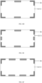
- FIG. 5A and FIG. 5B show a schematic diagram of a planar arrangement of spacers 30 in a touch panel.
- the at least one spacer 30 includes a plurality of spacers 30, the plurality of spacers 30 are arranged at intervals on edges of the second substrate 20 and the control substrate.
- plane shapes of the second substrate 20 and the control substrate are rectangular, and the plurality of spacers 30 are arranged in a straight line along at least two sides of the rectangle.
- the planar shapes of the second substrate 20 and the control substrate are rectangular, and each of the spacers 30 has a structure of a straight line, and the spacers are arranged along the four sides of the rectangle respectively, for example, the spacers 30 are arranged in the middle of the four sides.
- the touch circuit layer 11 is arranged in the middle of the first substrate 10, that is, edges of the first substrate 10 are exposed, at this time, the plurality of spacers 30 may be directly arranged on the first substrate 10, so that the plurality of spacers 30 may be directly interposed between the second substrate 20 and the first substrate 10.
- FIG. 5A the touch circuit layer 11 is arranged in the middle of the first substrate 10, that is, edges of the first substrate 10 are exposed, at this time, the plurality of spacers 30 may be directly arranged on the first substrate 10, so that the plurality of spacers 30 may be directly interposed between the second substrate 20 and the first substrate 10.
- an arrangement range of the touch circuit layer 11 and an arrangement range of the first substrate 10 are basically the same, at this time, the plurality of spacers 30 may be directly arranged on the touch circuit layer 11, so that the plurality of spacers 30 may be directly sandwiched between the touch circuit layer 11 and the first substrate 10.
- FIG. 6A and FIG. 6B show another schematic diagram of an arrangement of spacers 30 in a touch panel.
- planar shapes of the second substrate 20 and the control substrate are rectangular
- the plurality of spacers 30 include four spacers 30, and the four spacers 30 are L-shaped and arranged along the four corners of the rectangle respectively, in this way, a better supporting effect can thus be provided.
- the touch circuit layer 11 is arranged in the middle of the first substrate 10, at this time, the four spacers 30 may be directly arranged at the four corners of the first substrate 10, so that the four spacers 30 may be directly sandwiched between the second substrate 20 and the first substrate 10.
- an arrangement range of the touch circuit layer 11 and the first substrate 10 is basically the same, at this time, the plurality of spacers 30 may be directly arranged at the four corners of the touch circuit layer 11, so that the four spacers 30 may be directly sandwiched between the touch circuit layer 11 and the first substrate 10.
- a height of each of the spacers 30 may be from 0.5mm to 10mm, such as 2mm, 4mm, 6mm or 8mm.
- the touch panel does not deform seriously and then the structure of the touch panel (such as, the glass substrate) will not be damaged due to excessive pressing force, and in the case that the heights of the spacers 30 are less than 0.5 mm, misoperation with a small pressure will be sensed by the touch panel, resulting in inaccurate sensing by the touch panel.
- the widths W1 of the spacers 30 may be from 2mm to 10mm, such as 3mm, 5mm, 7mm or 9mm.
- the spacers 30 can not only play a function of spacing, but also ensure that the first substrate 10 and the second substrate 20 are in a free vibration state, so that interference with the vibration modes is avoided.
- the plurality of spacers 30 include four spacers 30, the rectangle includes two opposite long sides S1 and two opposite short sides S2, each of the four spacers 30 has a structure of a straight line, and the four spacers are arranged along the two long sides S1 of the rectangle respectively, and each of the two long sides S1 is arranged with two spacers 30 correspondingly.
- a length of each of the long sides S1 is L
- each of the long sides S1 has a first end point T1 and a second end point T2
- a distance between the first end point T1 and a central axis of one spacer of the two spacers 30 close to the first end point T1 perpendicular to each of the long sides S1 is from 1/4L to 1/3L (1/4L is shown in the figure as an example)
- a distance between the second end point T2 and a central axis of one spacer of the two spacers 30 close to the second end point T2 perpendicular to each of the long sides S1 is from 1/4L to 1/3L (1/4L is shown in the figure as example).
- the lengths of the long sides S1 of the rectangle are L respectively
- the lengths of the short sides S2 of the rectangle are W respectively
- the length of each spacer 30 in the plurality of spacers 30 is from 0.1L to 0.5L, such as 0.2L, 0.3L or 0.4L
- the width is from 0.01W to 0.10W, such as 0.02W, 0.03W or 0.05W. In this way, a better septum effect can be achieved.
- the number of the spacers 30 may also be more, such as six, eight or ten.
- the number of the spacers 30 may be six, the six spacers 30 are respectively located at the four corners of the rectangle and the middle positions of the two opposite long sides; or in some other embodiments, as shown in FIG. 6E , the number of the spacers may also be eight, The eight spacers 30 are respectively located at the four corners of the rectangle and the middle positions of the two opposite long sides and the middle positions of the two opposite short sides; or in some other embodiments, as shown in FIG.
- the number of the spacers may be eight, the eight spacers 30 are respectively located at the four corners of the rectangle and on the two opposite long sides, for example, two spacers are arranged on each of the long sides; or in some other embodiments, as shown in FIG. 6G , the number of the spacers 30 may also be ten, the ten spacers 30 are respectively located at the four corners of the rectangle and on the two opposite long sides and the two opposite short sides; and two spacers are arranged on each of the long sides, and one spacer is arranged on each of the short sides.
- the embodiments of the present disclosure do not limit the number of the spacers arranged on each of the long sides and each of the short sides, for example, two spacers may also be arranged on each of the long sides and each of the short sides, or spacers may also be arranged at the four corners at the same time, and two spacers are arranged on each of the long sides and each of the short sides.
- two spacers may also be arranged on each of the long sides and each of the short sides, or spacers may also be arranged at the four corners at the same time, and two spacers are arranged on each of the long sides and each of the short sides.
- Whether to arrange spacers on each of the long sides and each of the short sides, and the number of the arranged spacers, whether to arrange spacers on each of the corners may be arranged according to the lengths of each of the long sides and each of the short sides and specific needs.
- the Young's modulus of the material of the spacers 30 is from 0.1MPa to 2.0MPa, such as 0.3MPa, 0.6MPa, 1.0MPa or 1.5MPa.
- the material of the spacer 30 may adopt foam, polydimethylsiloxane (PDMS) and other materials with certain elasticity, so that the noise generated by vibration and friction can be reduced in a case that the touch panel vibrates.
- PDMS polydimethylsiloxane
- FIG. 7A shows a cross-sectional schematic diagram of the piezoelectric layer 201, as shown in FIG. 7A , in some embodiments, the piezoelectric layer 201 includes a first control electrode layer 2011, a second control electrode layer 2013, and a piezoelectric material layer 2012 between the first control electrode layer 2011 and the second control electrode layer 2013.
- FIG. 7B shows a planar schematic diagram of the first control electrode layer 2011.
- the first control electrode layer 2011 includes a plurality of first pressure sensing electrodes 2011B arranged at intervals, at least one of the plurality of first pressure sensing electrodes 2011B is configured to transmit a pressure sensing signal to the control circuit 110 in a case that the piezoelectric material layer 2012 is under pressure.
- the first control electrode layer 2011 further includes a plurality of first vibration feedback electrodes 2011A arranged at intervals
- the control circuit 110 is configured to apply an electrical signal to at least one of the plurality of first vibration feedback electrodes 2011A in a case that the pressure sensing signal is greater than a threshold, to drive the piezoelectric material layer 2012 to vibrate.
- the piezoelectric layer 201 is simultaneously used as a pressure detection layer and a tactile vibration feedback layer, and the touch panel can provide vibration tactile sensation while touching, so as to realize pressing-key confirmation and shortcut operation.
- the control circuit detects the "touch behavior"
- the control circuit excites the vibration feedback electrode with an electric signal, causing the piezoelectric material layer 2012 to vibrate, in turn, the touch panel is caused to resonate, resulting in large displacement and acceleration, so that a vibration tactile sensation is provided.
- a vibration frequency of the piezoelectric material layer 2012 may be controlled within a range of 50Hz to 600Hz.
- the human body is more sensitive to the vibration touch in the range of 50Hz to 1000Hz, that is, the human body is more likely to perceive the vibration, and is not sensitive to the vibration in the range of 30Hz to 600Hz, that is, the human body is not easy to hear the vibration in the range of 30Hz to 600Hz, thus the vibration frequency of the piezoelectric material layer 2012 may be controlled within the range of 50Hz to 600Hz, in this way, the human body can more easily sense the sense of touch without hearing the vibration.
- the plurality of first pressure sensing electrodes 2011B and the plurality of first vibration feedback electrodes 2011A may be strip electrodes, the strip electrodes extend along a first direction (a vertical direction in FIG. 7B ), and are arranged at intervals in a second direction (a horizontal direction in FIG. 7B ) perpendicular to the first direction.
- the plurality of first pressure sensing electrodes 2011B and the plurality of first vibration feedback electrodes 2011A that are arranged above have a relatively large overlapping area with the piezoelectric material layer 2012, thus an effective use area of the piezoelectric material layer 2012 can be increased.
- first vibration feedback electrodes 2011A and seven columns of first pressure sensing electrodes 2011B are shown in the embodiment of FIG. 7B as an example, but the embodiments of the present disclosure do not limit the number of the first vibration feedback electrodes 2011A and the number of the first pressure sensing electrodes 2011B, which may be selected according to factors such as a size of the touch panel.
- the plurality of first pressure sensing electrodes 2011B and the plurality of first vibration feedback electrodes 2011A are arranged alternately in the second direction.
- one column of first vibration feedback electrodes 2011A is arranged between two adjacent columns of first pressure sensing electrodes 2011B, and one column of first pressure sensing electrodes 2011B is arranged between adjacent first vibration feedback electrodes 2011A.
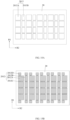
- FIG. 8 shows another planar schematic diagram of the first control electrode layer, as shown in FIG. 8
- each of the plurality of first pressure sensing electrodes 2011B includes a plurality of sub-strip electrodes 2011B1 spaced along the first direction (two sub-strip electrodes 2011B1 are shown in the figure as an example);
- each of the plurality of first vibration feedback electrodes 2011A includes a plurality of sub-strip electrodes 2011A1 spaced along the first direction (two sub-strip electrodes 2011A1 are shown in the figure as an example).
- further separation of the tactile feedback and pressure sensing region can be achieved, so that it is beneficial to partition control and realize more kinds of modal vibrations.
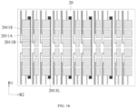
- FIG. 9 shows another planar schematic diagram of the first control electrode layer, as shown in FIG. 9
- the plurality of first pressure sensing electrodes 2011B and the plurality of first vibration feedback electrodes 2011A are block electrodes
- the plurality of first pressure sensing electrodes 2011B are spaced apart and arranged in a column along the first direction R1 (a vertical direction in FIG. 9 )
- a plurality of first vibration feedback electrodes 2011A are spaced apart and arranged in a column along the first direction R1
- multiple columns of the first pressure sensing electrodes 2011B and multiple columns of the first vibration feedback electrodes 2011A are arranged alternately along a second direction R2 (a horizontal direction in FIG. 9 ) perpendicular to the first direction R1.
- a plurality of first pressure sensing electrodes 2011B in a same column are electrically connected, and are electrically connected with the touch circuit 110 at a bonding region B located at an edge of the piezoelectric layer; a plurality of first vibration feedback electrodes 2011A located in a same column are electrically connected, and are electrically connected with the touch circuit 110 at a bonding region B located at an edge of the piezoelectric layer.
- each of the first pressure sensing electrodes 2011B and each of first vibration feedback electrodes 2011A may be electrically connected with the touch circuit 110 respectively; or the plurality of first pressure sensing electrodes 2011B in the same column are electrically connected with the touch circuit 110 in different regions respectively, and the plurality of first vibration feedback electrodes 2011A located in the same column are electrically connected with the touch circuit 110 in different regions respectively.
- the plurality of first pressure sensing electrodes 2011B and the plurality of first vibration feedback electrodes 2011A of the first control electrode layer form a rectangular matrix, and electrical connection structures among the adjacent first pressure sensing electrodes 2011B and the adjacent first vibration feedback electrodes 2011A are relatively narrow, thus in a case that a portion of the pattern of the piezoelectric material layer 2012 (to be introduced later) is short-circuited, the electrodes above the short-circuited part of the piezoelectric material layer 2012 may be cut off by means of cutting off and repairing, so that the portion of the piezoelectric material layer 2012 that is short-circuited no longer participates in the sensing work, in this way, other parts of the piezoelectric material layer 2012 can be guaranteed to continue to work normally.
- a width W2 of each of the plurality of first vibration feedback electrodes 2011A in the second direction R2 is larger than a width W3 of each of the plurality of first pressure sensing electrodes 2011B in the second direction R2.
- the piezoelectric material layer 2012 may be arranged on the entire surface, that is, the piezoelectric material layer 2012 is arranged continuously as a whole, and is arranged on the second control electrode layer 2013 in a sheet shape.
- the piezoelectric material layer 2012 includes a plurality of piezoelectric material patterns 2012A, the plurality of piezoelectric material patterns 2012A extend along the first direction R1 and are arranged at intervals in the second direction R2, orthographic projections of the plurality of piezoelectric material patterns 2012A on the second substrate 20 are at least partially overlapped with the orthographic projections of the plurality of first pressure sensing electrodes 2021B and the plurality of first vibration feedback electrodes 2021A on the second substrate 20 respectively.
- a pattern shape and a size of each of the plurality of piezoelectric material patterns 2012A are basically the same as a pattern shape and a size of each of the plurality of first pressure sensing electrodes 2021B and each of the plurality of first vibration feedback electrodes 2021A, respectively, thus in the manufacturing process, the plurality of piezoelectric material patterns 2012A and the plurality of first pressure sensing electrodes 2021B and the plurality of first vibration feedback electrodes 2021A may be formed in a same patterning process by using a same mask, to simplify the manufacturing process of the touch panel.
- the material of the piezoelectric material layer 2012 is one or more of PZT (lead zirconate titanate), AlN (aluminum nitride) and KNN [(K 0.5 Na 0.5 )NbO 3 ].
- PZT lead zirconate titanate
- AlN aluminum nitride
- KNN KNN [(K 0.5 Na 0.5 )NbO 3 ].
- the above materials all have a piezoelectric effect, which can realize the mutual conversion of mechanical energy and electrical energy.
- An electrical signal can be generated under pressure or a material can be mechanically deformed under an electric field.
- PZT has the advantages of high piezoelectric constant and high Curie temperature.
- AlN and KNN are lead-free piezoelectric materials, which are more green and environmentally friendly. Forming the piezoelectric material layer 2012 by using the above materials can improve the sensitivity of pressure sensing.
- the second control electrode layer 2013 is a surface electrode layer, that is, the second control electrode layer 2013 is arranged continuously as a whole, and is arranged in a sheet shape, for example, on the second substrate 20.
- the second control electrode layer 2013 is a surface electrode layer, and the piezoelectric material layer 2012 is arranged on the whole surface, and exposes an edge of the second control electrode layer 2013, that is, the piezoelectric material layer 2012 shrinks inward relative to the second control electrode layer 2013, so that the second control electrode layer 2013 is exposed at the edge of the second control electrode layer 2013.
- the second control electrode layer 2013 it is helpful for the second control electrode layer 2013 to be electrically connected to the touch circuit 110.
- the second control electrode layer 2013 to be electrically connected with the touch circuit 110.
- the pattern and the size of each of the plurality of second control electrodes 2013A are substantially the same as the pattern and the size of each of the plurality of first pressure sensing electrodes 2011B and each of the plurality of first vibration feedback electrodes 2011A respectively, or the patterns of each of the plurality of second control electrodes 2013A are substantially the same as the patterns of each of the plurality of first pressure sensing electrodes 2011B and each of the plurality of first vibration feedback electrodes 2011A respectively, the dimensions are respectively slightly larger than the dimensions of the plurality of first pressure sensing electrodes 2011B and the plurality of first vibration feedback electrodes 2011A, so that the second control electrodes 2013A can be better overlapped with the plurality of first pressure sensing electrodes 2011B and the plurality of first vibration feedback electrodes 2011A.
- the pressure sensor sensitive element 40 may be a commercially available device, and be bonded on the touch substrate with an optically clear adhesive (OCA), for example, bonded on the control circuit layer 11 or the first substrate 10, and are electrically connected with the control circuit.
- OCA optically clear adhesive
- the pressure sensor sensitive element 40 is triggered to generate a voltage change and transmit an electrical signal to the control circuit.
- FIG. 12B and FIG. 12C show planar schematic diagrams of the pressure sensor sensitive elements 40.
- the at least one pressure sensor sensitive element 40 includes a plurality of pressure sensor sensitive elements 40, both the pressure sensor sensitive elements 40 and the spacers 30 are arranged on the control substrate, for example, arranged on the first substrate 10 (a situation shown in FIG. 12B ) or on the control circuit layer 11 (a situation shown in FIG. 12C ), and are arranged on an edge of the first substrate 10 or the control circuit layer 11.
- the control circuit layer 11 is arranged in the middle of the first substrate 10, thus the pressure sensor sensitive elements 40 may be directly arranged between the second substrate 20 and the first substrate 10, for example, arranged on edges of the four sides of the first substrate 10; in the embodiment shown in FIG. 12C , an arrangement range of the control circuit layer 11 on the first substrate 10 is basically the same, thus the pressure sensor sensitive elements 40 are directly arranged between the control circuit layer 11 and the first substrate 10, for example, arranged on the edges of the four sides of the control circuit layer 11.
- FIG. 12B and FIG. 12C are illustrated by taking the pressure sensor sensitive elements 40 arranged on the edge of the four sides of the first substrate 10 or the four sides of the control circuit layer 11 as an example, in other embodiments, the pressure sensor sensitive elements 40 may also be arranged at the four corners of the first substrate 10 or the control circuit layer 11, at this time, the spacers 30 are arranged on four sides of the first substrate 10 or the control circuit layer 11.
- the pressure sensor sensitive element 40 since the height H2 of the pressure sensor sensitive element 40 is lower than the height H2 of each of the spacers 30, the pressure sensor sensitive element 40 is spaced apart from the second substrate 20, as shown in FIG. 12A , in a case that the touch panel is not subjected to an external force, the pressure sensor sensitive element 40 will not be triggered, and in a case that the touch panel is subjected to an external force, the second substrate 20 is deformed to touch the pressure sensor sensitive element 40, thus the pressure sensor sensitive element 40 will sense the pressure, realize the piezoelectric conversion, and transmit the electric signal to the touch circuit 110.
- the first touch electrode layer 2021 and the second touch electrode layer 2023 are made of transparent metal oxide materials such as indium tin oxide (ITO), the interval insulating layer 2022 may use optical clear adhesive (OCA), so that the interval insulating layer 2022 can simultaneously play the roles of spacer, insulation and adhesion.
- transparent metal oxide materials such as indium tin oxide (ITO)
- the interval insulating layer 2022 may use optical clear adhesive (OCA), so that the interval insulating layer 2022 can simultaneously play the roles of spacer, insulation and adhesion.
- OCA optical clear adhesive
- the first touch electrode layer 2021 and the second touch electrode layer 2023 may be directly deposited on the second substrate 20 by magnetron sputtering or sol-gel or aerosol method, in a case that the piezoelectric material layer 2012 is formed after the first touch electrode layer 2021 and the second touch electrode layer 2023 are formed, since heat treatment temperature of the piezoelectric material layer 2012 is generally greater than 500 degrees, at this time, the interval insulating layer 2022 may also use inorganic insulating materials such as silicon oxide, silicon nitride or silicon oxynitride, to avoid being melted.
- the touch layer may be implemented as a projected capacitive touch layer, the touch electrodes intersecting in the first direction R1 and the second direction R2 form a capacitance matrix, and by detecting the change of the capacitances of the touch positions, the coordinates of the touch positions are calculated.
- the object such as the finger will form capacitor with the first touch electrodes 2021A and the second touch electrodes 2022B, so that the original capacitive structure of the first touch electrodes 2021A and the second touch electrodes 2022B will be changed, by detecting abscissa and ordinate of the first touch electrodes 2021A and the second touch electrodes 2022B whose capacitance have been changed respectively, the touch position of the object such as the finger can be determined, so that touch detection is realized.
- the second substrate 20 may be a rigid substrate, such as a non-metallic substrate such as a glass, a quartz substrate or a plastic substrate, or a metal substrate such as an aluminum substrate and an aluminum alloy substrate; or the second substrate 20 may also be a flexible substrate, such as an insulating substrate formed of an organic insulating material such as polyimide.
- the touch layer 202 and the piezoelectric layer 201 may be manufactured on the second substrate 20 respectively, and are attached to the touch substrate as a whole with the second substrate 20.
- the first substrate 10 may be a rigid substrate, such as a non-metallic substrate such as a glass, a quartz substrate or a plastic substrate, or a metal substrate such as an aluminum substrate and an aluminum alloy substrate, to provide better support and protection.
- a rigid substrate such as a non-metallic substrate such as a glass, a quartz substrate or a plastic substrate, or a metal substrate such as an aluminum substrate and an aluminum alloy substrate, to provide better support and protection.
- the first control electrode layer, the piezoelectric material layer and the second control electrode layer may adopt different patterns and connection manners.
- FIG. 14A to FIG. 14E are planar schematic diagrams of various layers of a piezoelectric layer in a touch panel provided by an embodiment of the present disclosure.
- the number of second control electrode patterns 2013B is smaller than the number of second control electrode patterns 2013A.
- the plurality of second control electrode patterns 2013A located in the same column are electrically connected with each other and are connected with the second control electrode patterns 2013C; the number of the second control electrode patterns 2013B located in a same column is two, and the second control electrode patterns 2013B are located at the head and the end of the column.
- the patterns and the sizes of the second control electrode patterns 2013A are substantially the same as the patterns and sizes of the second control electrode patterns 2013B.
- FIG. 14B shows a planar schematic diagram of a piezoelectric material layer 2012, as shown in FIG. 14B , the piezoelectric material layer 2012 includes a plurality of piezoelectric material patterns 2012A, and the plurality of piezoelectric material patterns 2012A are in one-to-one correspondence with and overlapped with the second control electrode pattern 2013A and the second control electrode pattern 2013B respectively.
- FIG. 14C shows a planar schematic diagram of the first control electrode layer 2011, as shown in FIG. 14C
- the first control electrode layer 2011 includes a plurality of first pressure sensing electrodes 2011B and a plurality of first vibration feedback electrodes 2011A
- the plurality of first pressure sensing electrodes 2011B and the plurality of first vibration feedback electrodes 2011A are overlapped with the plurality of piezoelectric material patterns 2012A in a one-to-one correspondence.
- a plurality of first pressure sensing electrodes 2011B together with a plurality of piezoelectric material patterns 2012A and a plurality of second control electrode patterns 2013B constitute a pressure sensing unit
- a plurality of first vibration feedback electrodes 20 11A together with a plurality of piezoelectric material patterns 2012A and a plurality of second control electrode patterns 2013A constitute a vibration feedback unit.
- FIG. 14D shows a planar schematic diagram of a first insulating layer 2014, as shown in FIG. 14D , the first insulating layer 2014 is arranged on the first control electrode layer 2011, and the first insulating layer 2014 includes a plurality of openings 2012B exposing the second control electrode patterns 2013C and a plurality of openings 2014A exposing the plurality of first vibration feedback electrodes 2011A and the plurality of first pressure sensing electrodes 2011B, and these openings are used for electrical connection of the wirings and the exposed structures.
- FIG. 14E shows a planar schematic diagram of a wiring layer
- the wiring layer includes a plurality of wirings 2015
- each of the wirings 2015 is used to electrically connect first pressure sensing electrodes 2011B located in a same column or first vibration feedback electrodes 2011A located in a same column, and is connected with the control circuit; or in other embodiments, each of the wirings 2015 may also be connected with one first vibration feedback electrode 2011A or one first pressure sensing electrode 2011B.
- Embodiments of the present disclosure do not limit the electrical connection manners of the plurality of wirings 2015 and the plurality of first vibration feedback electrodes 2011A and the plurality of first pressure sensing electrodes 2011B.
- FIG. 15A to FIG. 15E are planar schematic diagram of various layers of a piezoelectric layer in another touch panel provided by another embodiment of the present disclosure.
- FIG. 15A shows a planar schematic diagram of a second control electrode layer 2013, in this example, the second control electrode layer 2013 is arranged on the second substrate 20, the second control electrode layer 2013 includes a plurality of second control electrode patterns 2013A and 2013B, for example, the second control electrode patterns 2013A are used to be overlapped with the first vibration feedback electrodes 2011A, to realize the vibration feedback function, and the second control electrode patterns 2013B are used to be overlapped with the first pressure sensing electrodes 2011B, and are used to realize the pressure detection function.
- the number of the second control electrode patterns 2013B is equal to the number of the second control electrode patterns 2013A.
- the widths (areas) of the second control electrode patterns 2013A are larger than the widths (areas) of the second control electrode patterns 2013B.
- FIG. 15B shows a planar schematic diagram of a piezoelectric material layer 2012, as shown in FIG. 15B , the piezoelectric material layer 2012 includes a plurality of piezoelectric material patterns 2012A, 2012B, 2012C, and 2012D, the plurality of piezoelectric material patterns 2012A are respectively overlapped with the plurality of second control electrode patterns 2013A, and the plurality of piezoelectric material patterns 2012A are overlapped with the plurality of second control electrode patterns 2013B, respectively.
- the piezoelectric material patterns 2012D are used to be overlapped with the contact pad 2011D (described later) in the first control electrode layer 2011, the piezoelectric material patterns 2012C are used as connection structures for connecting two adjacent piezoelectric material patterns 2012A or two adjacent piezoelectric material patterns 2012B in the column direction, or connecting the piezoelectric material patterns 2012A or 2012B with the piezoelectric material patterns 2012D.
- FIG. 15C shows a planar schematic diagram of a first control electrode layer 2011, as shown in FIG. 15C , the first control electrode layer 2011 includes a plurality of first pressure sensing electrodes 2011B, a plurality of first vibration feedback electrodes 2011A, a connection electrode 2011C and a contact pad 2011D.
- the plurality of first pressure sensing electrodes 2011B and the plurality of first vibration feedback electrodes 2011A are overlapped with the plurality of piezoelectric material patterns 2012A and 2012B, respectively.
- the plurality of first pressure sensing electrodes 2011B together with the plurality of piezoelectric material patterns 2012B and the plurality of second control electrode patterns 2013B constitute a pressure sensing unit
- the plurality of first vibration feedback electrodes 2011A together with the plurality of piezoelectric material patterns 2012A and the plurality of second control electrode patterns 2013A constitute a vibration feedback unit.
- the plurality of first pressure sensing electrodes 2011B and the plurality of first vibration feedback electrodes 2011A are divided into two regions, that is, an upper half region G1 and a lower half region G2 in the figure, the first pressure sensing electrodes 2011B located in a same region and in a same column are electrically connected by the connection electrodes 2011C, and are connected with the corresponding contact pad 2011D; the first vibration feedback electrodes 2011A located in the same region and in the same column are electrically connected by the connection electrodes 2011C, and are connect with the corresponding contact pad 2011D.
- the first control electrode layer and the second control electrode layer may also be electrically connected with the control circuit in other ways, and the piezoelectric material layer may also be arranged in other ways, which will not be repeated herein.
Landscapes
- Engineering & Computer Science (AREA)
- General Engineering & Computer Science (AREA)
- Theoretical Computer Science (AREA)
- Human Computer Interaction (AREA)
- Physics & Mathematics (AREA)
- General Physics & Mathematics (AREA)
- Quality & Reliability (AREA)
- Computer Networks & Wireless Communication (AREA)
- Position Input By Displaying (AREA)
- Switches That Are Operated By Magnetic Or Electric Fields (AREA)
Abstract
Description
- At least one embodiment of the present disclosure relates to a touch panel.
- A touchpad is an input device that can move a cursor by sliding the finger, for example the touchpad is used in the devices such as laptops or keyboards. The touchpad is used to know the movement of the finger through capacitive sensing, in a case that a user's finger touches the touchpad, capacitance of the touched position will change, the touch panel will detect the capacitance change and convert it into coordinates to realize touch operation.
- At least one embodiment of the present disclosure provides a touch panel, the touch panel comprises a control substrate, a touch layer and a piezoelectric layer that are stacked, the control substrate comprises a first substrate and a control circuit layer arranged on the first substrate, and the touch layer and the piezoelectric layer are located on the control substrate, the control circuit layer comprises a control circuit, and the control circuit is electrically connected with the touch layer and the piezoelectric layer respectively, and is configured to apply electrical signals to the touch layer and the piezoelectric layer and/or receive electrical signals from the touch layer and the piezoelectric layer respectively.
- For example, the touch panel provided by at least one embodiment of the present disclosure further comprises a second substrate, the touch layer and the piezoelectric layer are arranged on the second substrate, and the second substrate, the touch layer and the piezoelectric layer are arranged as a whole on a side of the control circuit layer away from the first substrate.
- For example, the touch panel provided by at least one embodiment of the present disclosure further comprises at least one spacer arranged between the second substrate and the control substrate, to space the second substrate and the control substrate.
- For example, in the touch panel provided by at least one embodiment of the present disclosure, the at least one spacer comprises a plurality of spacers, and the plurality of spacers are arranged at intervals on edges of the second substrate and the control substrate.
- For example, in the touch panel provided by at least one embodiment of the present disclosure, planar shapes of the second substrate and a plane shape of the control substrate are rectangles, and each of the plurality of spacers is shaped in a straight line and the plurality of spacers are disposed along at least two sides of the rectangle respectively.
- For example, in the touch panel provided by at least one embodiment of the present disclosure, the plurality of spacers comprise four spacers, each of the four spacers has a shape of a straight line, and the four spacers are disposed at middle positions of four sides of the rectangle respectively.
- For example, in the touch panel provided by at least one embodiment of the present disclosure, the plurality of spacers comprise four spacers, and the rectangle comprises two opposite long sides and two opposite short sides, and each of the four spacers has a shape of a straight line, and the four spacers are arranged along the two long sides of the rectangle, and two spacers are correspondingly arranged on each of the two long sides.
- For example, in the touch panel provided by at least one embodiment of the present disclosure, a length of each of the long sides is L, and each of the long sides has a first end point and a second end point, and a distance between the first end point and a central axis of one of the two spacers close to the first end point perpendicular to each of the long sides is from 1/4L to 1/3L, and a distance between the second end point and a central axis of one of the two spacers close to the second end point perpendicular to each of the long sides is from 1/4L to 1/3L.
- For example, in the touch panel provided by at least one embodiment of the present disclosure, a length of the long side of the rectangle is L, and a length of the short side is W, a length of each spacer in the plurality of spacers is from 0.1L to 0.5L, and a width of each spacer in the plurality of spacers is from 0.01W to 0.10W.
- For example, in the touch panel provided by at least one embodiment of the present disclosure, planar shapes of the second substrate and the control substrate are rectangles, and the plurality of spacers comprise four spacers, and each of the four spacers is shaped in an L shape and are disposed along four corners of the rectangle.
- For example, in the touch panel provided by at least one embodiment of the present disclosure, in a direction perpendicular to the second substrate, a height of the at least one spacer is from 0.5mm to 10mm.
- For example, in the touch panel provided by at least one embodiment of the present disclosure, Young's modulus of material of the at least one spacer is from 0.1MPa to 2.0MPa.
- For example, the touch panel provided by at least one embodiment of the present disclosure further comprises at least one pressure sensor sensitive element arranged between the second substrate and the control substrate, the at least one pressure sensor sensitive element is electrically connected with the control circuit, and in a direction perpendicular to the second substrate, a height of the at least one pressure sensor sensitive element is lower than a height of the at least one spacer.
- For example, in the touch panel provided by at least one embodiment of the present disclosure, the at least one pressure sensor sensitive element and the at least one spacer are both arranged on the control substrate, and the at least one pressure sensor sensitive element is separated from the second substrate.
- For example, in the touch panel provided by at least one embodiment of the present disclosure, the piezoelectric layer comprises a first control electrode layer, a second control electrode layer, and a piezoelectric material layer between the first control electrode layer and the second control electrode layer, the first control electrode layer comprises a plurality of first pressure sensing electrodes arranged at intervals, at least one of the plurality of first pressure sensing electrodes is configured to transmit a pressure sensing signal to the control circuit in a case that the piezoelectric material layer is under pressure.
- For example, in the touch panel provided by at least one embodiment of the present disclosure, the first control electrode layer further comprises a plurality of first vibration feedback electrodes arranged at intervals, the control circuit is configured to apply an electrical signal to at least one of the plurality of first vibratory feedback electrodes in a case that the pressure sensing signal is greater than a threshold, to drive the piezoelectric material layer to vibrate.
- For example, in the touch panel provided by at least one embodiment of the present disclosure, the plurality of first pressure sensing electrodes and the plurality of first vibration feedback electrodes are strip-shaped electrodes, and the strip-shaped electrodes extend along a first direction and are arranged at intervals in a second direction which is perpendicular to the first direction.
- For example, in the touch panel provided by at least one embodiment of the present disclosure, the plurality of first pressure sensing electrodes and the plurality of first vibration feedback electrodes are arranged alternately in the second direction.
- For example, in the touch panel provided by at least one embodiment of the present disclosure, each of the plurality of first pressure sensing electrodes comprises a plurality of sub-strip electrodes spaced along the first direction; and each of the plurality of first vibration feedback electrodes comprises a plurality of sub-strip electrodes spaced along the first direction.
- For example, in the touch panel provided by at least one embodiment of the present disclosure, the plurality of first pressure sensing electrodes and the plurality of first vibration feedback electrodes are block-shaped electrodes, the plurality of first pressure sensing electrodes are spaced along the first direction and are arranged in a column, the plurality of first vibration feedback electrodes are spaced along the first direction and are arranged in a column, and a plurality of columns of first pressure sensing electrodes and a plurality of columns of first vibration feedback electrodes are arranged alternately along a second direction perpendicular to the first direction.
- For example, in the touch panel provided by at least one embodiment of the present disclosure, a width of each of the plurality of first vibration feedback electrodes in the second direction is greater than a width of each of the plurality of first pressure sensing electrodes in the second direction.
- For example, in the touch panel provided by at least one embodiment of the present disclosure, the piezoelectric material layer is arranged on an entire surface.
- For example, in the touch panel provided by at least one embodiment of the present disclosure, the piezoelectric material layer comprises a plurality of piezoelectric material patterns, the plurality of piezoelectric material patterns extend along the first direction, and are arranged at intervals in the second direction, orthographic projections of the plurality of piezoelectric material patterns on the second substrate are at least partially overlapped with orthographic projections of the plurality of first pressure sensing electrodes and the plurality of first vibration feedback electrodes on the second substrate.
- For example, in the touch panel provided by at least one embodiment of the present disclosure, the second control electrode layer is a surface electrode layer; or the second control electrode layer comprises a plurality of second control electrodes, orthographic projections of the plurality of second control electrodes on the second substrate are at least partially overlapped with orthographic projections of the plurality of first pressure sensing electrodes and orthographic projections of the plurality of first vibration feedback electrodes respectively on the second substrate.
- For example, in the touch panel provided by at least one embodiment of the present disclosure, a material of the piezoelectric material layer is one or more of PZT, AlN and KNN.
- For example, in the touch panel provided by at least one embodiment of the present disclosure, the touch layer comprises a first touch electrode layer, a second touch electrode layer, and an interval insulating layer between the first touch electrode layer and the second touch electrode layer, the first touch electrode layer comprises a plurality of first touch electrodes extending along a first direction, and the second touch electrode layer comprises a plurality of second touch electrodes extending along a second direction intersecting the first direction.
- For example, in the touch panel provided by at least one embodiment of the present disclosure, the touch layer and the piezoelectric layer are respectively arranged on two opposite sides of the second substrate.
- For example, in the touch panel provided by at least one embodiment of the present disclosure, the touch layer and the piezoelectric layer are respectively arranged on a same side of the second substrate, and the touch panel further comprises an electromagnetic shielding layer arranged between the touch layer and the piezoelectric layer.
- For example, in the touch panel provided by at least one embodiment of the present disclosure, the touch layer is arranged on a side of the piezoelectric layer away from the control substrate, the touch panel further comprises a cover plate on a surface of the touch layer away from the control substrate, and a surface of the cover plate away from the control substrate becomes a touch surface of the touch panel.
- In order to clearly illustrate the technical solution of the embodiments of the present disclosure, the drawings of the embodiments will be briefly described. It is obvious that the described drawings in the following are only related to some embodiments of the present disclosure and thus are not construed as any limitation to the present disclosure.
-
FIG. 1 is a schematic structural diagram of a touch panel provided by at least one embodiment of the present disclosure; -
FIG. 2 is a cross-sectional schematic diagram of a touch layer and a piezoelectric layer in a touch panel provided by at least one embodiment of the present disclosure; -
FIG. 3 is a cross-sectional schematic diagram of a touch layer and a piezoelectric layer in another touch panel provided by at least one embodiment of the present disclosure; -
FIG. 4 is a cross-sectional schematic diagram of a touch panel provided by at least one embodiment of the present disclosure; -
FIG. 5A is a schematic diagram of a planar arrangement of a plurality of spacers in a touch panel provided by at least one embodiment of the present disclosure; -
FIG. 5B is a schematic diagram of another planar arrangement of a plurality of spacers in a touch panel provided by at least one embodiment of the present disclosure; -
FIG. 6A is a schematic diagram of still another planar arrangement of a plurality of spacers in a touch panel provided by at least one embodiment of the present disclosure; -
FIG. 6B is a schematic diagram of still another planar arrangement of a plurality of spacers in a touch panel provided by at least one embodiment of the present disclosure; -
FIG. 6C to FIG. 6G are schematic diagrams of various planar arrangements of a plurality of spacers in a touch panel provided by at least one embodiment of the present disclosure; -
FIG. 7A is a cross-sectional schematic diagram of a piezoelectric layer in a touch panel provided by at least one embodiment of the present disclosure; -
FIG. 7B is a planar schematic diagram of a first control electrode layer of a piezoelectric layer in a touch panel provided by at least one embodiment of the present disclosure; -
FIG. 8 is another planar schematic diagram of a first control electrode layer of a piezoelectric layer in a touch panel provided by at least one embodiment of the present disclosure; -
FIG. 9 is still another planar schematic diagram of a first control electrode layer of a piezoelectric layer in a touch panel provided by at least one embodiment of the present disclosure; -
FIG. 10 is another cross-sectional schematic diagram of a piezoelectric layer in a touch panel provided by at least one embodiment of the present disclosure; -
FIG. 11A is a planar schematic diagram of a second control electrode layer of a piezoelectric layer in a touch panel provided by at least one embodiment of the present disclosure; -
FIG. 11B is another planar schematic diagram of a second control electrode layer of a piezoelectric layer in a touch panel provided by at least one embodiment of the present disclosure. -
FIG. 12A is another cross-sectional schematic diagram of a touch panel provided by at least one embodiment of the present disclosure; -
FIG. 12B is a schematic diagram of a planar arrangement of pressure sensor sensitive elements in a touch panel provided by at least one embodiment of the present disclosure; -
FIG. 12C is another schematic diagram of a planar arrangement of pressure sensor sensitive elements in a touch panel provided by at least one embodiment of the present disclosure; -
FIG. 13A is a cross-sectional schematic diagram of a touch layer in a touch panel provided by at least one embodiment of the present disclosure; -
FIG. 13B is a planar schematic diagram of a touch layer in a touch panel provided by at least one embodiment of the present disclosure; -
FIG. 14A to FIG. 14E are planar schematic diagrams of each layer of a piezoelectric layer in a touch panel provided by at least one embodiment of the present disclosure; -
FIG. 15A to FIG. 15D are planar schematic diagrams of each layer of a piezoelectric layer in another touch panel provided by at least one embodiment of the present disclosure; and -
FIG. 16 is a planar schematic diagram of a first control electrode layer, a second control electrode layer and a wiring layer in a touch panel provided by at least one embodiment of the present disclosure. - In order to make objects, technical details and advantages of the embodiments of the present disclosure apparent, the technical solutions of the embodiments of the present disclosure will be described in a clearly and fully understandable way in connection with the drawings related to the embodiments of the present disclosure. It is obvious that the described embodiments are just a part but not all of the embodiments of the present disclosure. Based on the described embodiments herein, those skilled in the art can obtain other embodiment(s), without any inventive work, which should be within the scope of the present disclosure.
- Unless otherwise defined, all the technical and scientific terms used herein have the same meanings as commonly understood by one of ordinary skill in the art to which the present disclosure belongs. The terms, such as "first," "second," or the like, which are used in the description and the claims of the present disclosure, are not intended to indicate any sequence, amount or importance, but for distinguishing various components. The terms, such as "comprise/comprising," "include/including," or the like are intended to specify that the elements or the objects stated before these terms encompass the elements or the objects and equivalents thereof listed after these terms, but not preclude other elements or objects. The terms, such as "connect/connecting/connected," "couple/coupling/coupled" or the like, are not limited to a physical connection or mechanical connection, but may include an electrical connection/coupling, directly or indirectly. The terms, "on," "under," "left," "right," or the like are only used to indicate relative position relationship, and when the position of the object which is described is changed, the relative position relationship may be changed accordingly.
- In existing touch panels, a global touch panel uses a linear motor and a piezoelectric sheet to provide a sense of vibration and perform operations such as pressing key confirmation. However, both the linear motor and the piezoelectric sheet have disadvantages such as large volume, many components, complex modules, simple touch, and high driving voltage. For example, the linear motor generally includes structures such as a sensor, an actuator, a gasket, and a controller; the piezoelectric sheet usually includes structures such as a circuit board, a conductive cloth, a piezoelectric sheet, a multi-layer adhesive, and a metal plate; an overall thickness and an overall volume of these structures are large, and a lot of parts and components are provided, and matching structures are complicated, which are not conducive to an overall thin design of the touch panel.
- At least one embodiment of the present disclosure provides a touch panel, the touch panel includes a control substrate, a touch layer, and a piezoelectric layer which are stacked; the control substrate includes a first substrate and a control circuit layer arranged on the first substrate, the touch layer and the piezoelectric layer are arranged on the control substrate, the control circuit layer includes a control circuit, and the control circuit is electrically connected with the touch layer and the piezoelectric layer respectively, and is configured to apply electrical signals to the touch layer and the piezoelectric layer and/or receive electrical signals from the touch layer and the piezoelectric layer respectively.
- The touch panel provided by the embodiments of the present disclosure can realize global tactile feedback, that is, in the whole touch panel, the piezoelectric layer may sense a pressure applied on a surface of the touch panel, and convert the pressure into an electrical signal to provide it to the control circuit, then the control circuit may judge whether the pressure can realize a control operation according to the electric signal, for example, in a case that the electrical signal is greater than a threshold signal, the pressure is judged as the pressure which is exerted to achieve the control operation, at this time, the control circuit may control the piezoelectric layer to further provide vibration, so that richer pressure feeling and touch feeling are realized. On the other hand, the module structure of the touch panel is simple, and has the advantages of thinner, lighter, lower driving voltage, and lower power consumption.
- In the following, the touch panel provided by the embodiments of the present disclosure will be described in detail through several specific embodiments.
- At least one embodiment of the present disclosure provides a touch panel,
FIG. 1 is a schematic structural diagram of a touch panel provided by at least one embodiment of the present disclosure, andFIG. 2 is a cross-sectional schematic diagram of a touch layer and a piezoelectric layer in a touch panel provided by at least one embodiment of the present disclosure. As shown inFIG. 1 , the touch panel includes a control substrate, atouch layer 202 and apiezoelectric layer 201 which are stacked. The control substrate includes afirst substrate 10 and acontrol circuit layer 11 arranged on thefirst substrate 10, thetouch layer 202 and thepiezoelectric layer 201 are arranged on the control substrate. - The
control circuit layer 11 includes acontrol circuit 110, and thecontrol circuit 110 is electrically connected with thetouch layer 202 and thepiezoelectric layer 201 respectively, and is configured to respectively apply electrical signals to thetouch layer 202 and thepiezoelectric layer 201 and/or receive electrical signals from thetouch layer 202 and thepiezoelectric layer 201 respectively. In this way, thecontrol circuit 110 can control thetouch layer 202 to realize functions such as detecting touch positions, and can control thepiezoelectric layer 201 to realize functions such as pressure detection and vibration feedback. - A module structure of the touch panel provided by the embodiment of the present disclosure is simple, the touch panel does not have complicated alignment and assembly of the back adhesive and the conductive cloth, and has a lighter and thinner structure, for example, an overall thickness of the touch panel can be reduced to within 1mm, and a driving voltage of the touch panel is low (for example, the driving voltage is less than 24V), and its power consumption is small, thus the touch panel is more energy efficient. On the other hand, the touch panel can realize global tactile feedback, and at the same time the touch panel can realize functions such as touch control and pressure detection, vibration feedback, to improve user experience.
- For example, in some embodiments, the
control circuit layer 110 may also include structures such as a flexible circuit board (FPC) or an integrated circuit (IC), and thecontrol circuit layer 110 has a plurality of contact pads (such as gold fingers), for electrical connection with thetouch layer 202 and thepiezoelectric layer 201. - For example, in some embodiments, as shown in
FIG. 1 and FIG. 2 , the touch panel may further include asecond substrate 20, thetouch layer 202 and thepiezoelectric layer 201 are arranged on thesecond substrate 20, and thesecond substrate 20, thetouch layer 202 and thepiezoelectric layer 201 are arranged as a whole on a side of thecontrol circuit layer 11 away from thefirst substrate 10. - For example, in some embodiments, as shown in
FIG. 2 , thetouch layer 202 and thepiezoelectric layer 201 are respectively arranged on two opposite sides of thesecond substrate 20, so that thetouch layer 202 and thepiezoelectric layer 201 are spaced far apart, to avoid electromagnetic interference between thetouch layer 202 and thepiezoelectric layer 201. - For example, during the manufacturing process, the
touch layer 202 and thepiezoelectric layer 201 may be respectively formed on two opposite sides of thesecond substrate 20, in this way, the manufacturing process of the touch panel can be simplified, which avoids undesirable phenomena such as broken glass substrates due to multiple processes performed on a same side of the glass substrate in a case that thesecond substrate 20 is selected as a glass substrate. - For example, in some embodiments, the
touch layer 202 is arranged on a side of thepiezoelectric layer 201 away from thefirst substrate 10. For example, as shown inFIG. 2 , the touch panel may also include acover plate 203 on a surface of thetouch layer 202 away from the control substrate, thesurface 203A (an upper surface inFIG. 2 ) of thecover plate 203 away from the control substrate becomes a touch surface of the touch panel. For example, thecover plate 203 may be made of organic insulating materials such as PET or tempered glass, to have higher surface hardness. - For example,
FIG. 3 shows another structural schematic diagram of the touch layer and the piezoelectric layer in the touch panel. As shown inFIG. 3 , in other embodiments, thetouch layer 202 and thepiezoelectric layer 201 may also be respectively arranged on a same side of thesecond substrate 20. - For example, as shown in
FIG. 3 , the touch panel further includes anelectromagnetic shielding layer 203 arranged between thetouch layer 202 and thepiezoelectric layer 201. Since thetouch layer 202 and thepiezoelectric layer 201 are arranged on a same side of thesecond substrate 20, a distance between thetouch layer 202 and thepiezoelectric layer 201 is relatively short, and electromagnetic interference is likely to occur between thetouch layer 202 and thepiezoelectric layer 201, by arranging theelectromagnetic shielding layer 203 between thetouch layer 202 and thepiezoelectric layer 201, electromagnetic interference between thetouch layer 202 and thepiezoelectric layer 201 can be effectively prevented, so that it can be ensured that thetouch layer 202 and thepiezoelectric layer 201 respectively perform accurate touch sensing operations, pressure sensing, and vibration feedback operations. - For example, in some embodiments, the
electromagnetic shielding layer 203 may be arranged on thetouch layer 202, that is, arranged on a side of thetouch layer 202 close to thepiezoelectric layer 201. For example, in some embodiments, theelectromagnetic shielding layer 203 may include a metal material, such as a metal layer formed of a metal material such as copper, aluminum, titanium, or a conductive layer formed of a metal oxide material such as indium tin oxide (ITO). For example, theelectromagnetic shielding layer 203 may be grounded or be applied with a fixed low-level voltage. For example, a thickness (a dimension in the direction perpendicular to the second substrate 20) of theelectromagnetic shielding layer 203 may be from 200nm to 300nm, such as 220nm, 250nm or 280nm. - For example, as shown in
FIG. 3 , the touch panel may further include aninterval insulating layer 204 arranged between theelectromagnetic shielding layer 203 and thepiezoelectric layer 201, which is used to insulate theelectromagnetic shielding layer 203 and thepiezoelectric layer 201 to prevent signal crosstalk. For example, inorganic insulating materials such as silicon oxide, silicon nitride, or silicon oxynitride may be used for theinterval insulating layer 204. For example, a thickness (a dimension in the direction perpendicular to the second substrate 20) of theinterval insulating layer 204 may be from 150 nm to 250 nm, such as 180 nm, 200 nm or 230 nm. - For example, in the embodiment shown in
FIG. 3 , asurface 20A of thesecond substrate 20 away from the control substrate (an upper surface inFIG. 3 ) becomes a touch surface of the touch panel; or the touch panel may also include a tempered glass cover plate arranged on asurface 20A of thesecond substrate 20 away from the control substrate, the tempered glass cover plate has a thinner thickness and stronger hardness, which can improve a user's touch feeling, and can prevent the surface of the touch panel from being broken. - For example, in the embodiment of
FIG. 3 , thetouch layer 202 and thepiezoelectric layer 201 are located on a side of thesecond substrate 20 close to the control substrate, in some other embodiments, thetouch layer 202 and thepiezoelectric layer 201 may also be located on a side of the second substrate away from the control substrate, and are arranged in sequence along the direction away from the control substrate. For example, in the embodiment ofFIG. 2 , thetouch layer 202 is located on a side of thepiezoelectric layer 201 away from the control substrate, in other embodiments, thepiezoelectric layer 201 may also be located on a side of thetouch layer 202 away from the control substrate. - For example, in some other embodiments, the
touch layer 202 and thepiezoelectric layer 201 may also be arranged in the same layer, for example arranged side by side on thesecond substrate 20, for example, thetouch layer 202 and thepiezoelectric layer 201 respectively include a plurality of regions, a plurality of regions of thetouch layer 202 and a plurality of regions of thepiezoelectric layer 201 are intersected and (alternately) arranged on thesecond substrate 20, so that the plurality of regions of thetouch layer 202 and the plurality of regions of thepiezoelectric layer 201 are arranged in the same layer. Embodiments of the present disclosure do not specifically limit a specific arrangement of thetouch layer 202 and thepiezoelectric layer 201 and their positions relative to thesecond substrate 20. - For example,
FIG. 4 shows a cross-sectional schematic diagram of a touch panel provided by at least one embodiment of the present disclosure. In some embodiments, as shown inFIG. 4 , the touch panel may further include at least onespacer 30 arranged between thesecond substrate 20 and the control substrate, to separate thesecond substrate 20 from the control substrate. - For example, in some embodiments, the at least one
spacer 30 may be sandwiched between thesecond substrate 20 and thetouch circuit layer 11, or in some other embodiments, thetouch circuit layer 11 is arranged in the middle of thefirst substrate 10, at this time, the at least onespacer 30 may be interposed between thesecond substrate 20 and thefirst substrate 10. - For example,
FIG. 5A and FIG. 5B show a schematic diagram of a planar arrangement ofspacers 30 in a touch panel. As shown inFIG. 5A and FIG. 5B , the at least onespacer 30 includes a plurality ofspacers 30, the plurality ofspacers 30 are arranged at intervals on edges of thesecond substrate 20 and the control substrate. - For example, in some embodiments, plane shapes of the
second substrate 20 and the control substrate are rectangular, and the plurality ofspacers 30 are arranged in a straight line along at least two sides of the rectangle. - For example, as shown in
FIG. 5A and FIG. 5B , in some embodiments, the planar shapes of thesecond substrate 20 and the control substrate are rectangular, and each of thespacers 30 has a structure of a straight line, and the spacers are arranged along the four sides of the rectangle respectively, for example, thespacers 30 are arranged in the middle of the four sides. For example, in the embodiment shown inFIG. 5A , thetouch circuit layer 11 is arranged in the middle of thefirst substrate 10, that is, edges of thefirst substrate 10 are exposed, at this time, the plurality ofspacers 30 may be directly arranged on thefirst substrate 10, so that the plurality ofspacers 30 may be directly interposed between thesecond substrate 20 and thefirst substrate 10. In the embodiment ofFIG. 5B , an arrangement range of thetouch circuit layer 11 and an arrangement range of thefirst substrate 10 are basically the same, at this time, the plurality ofspacers 30 may be directly arranged on thetouch circuit layer 11, so that the plurality ofspacers 30 may be directly sandwiched between thetouch circuit layer 11 and thefirst substrate 10. - For example,
FIG. 6A andFIG. 6B show another schematic diagram of an arrangement ofspacers 30 in a touch panel. As shown inFIG. 6A andFIG. 6B , planar shapes of thesecond substrate 20 and the control substrate are rectangular, the plurality ofspacers 30 include fourspacers 30, and the fourspacers 30 are L-shaped and arranged along the four corners of the rectangle respectively, in this way, a better supporting effect can thus be provided. - For example, in the embodiment shown in
FIG. 6A , thetouch circuit layer 11 is arranged in the middle of thefirst substrate 10, at this time, the fourspacers 30 may be directly arranged at the four corners of thefirst substrate 10, so that the fourspacers 30 may be directly sandwiched between thesecond substrate 20 and thefirst substrate 10. In the embodiment ofFIG. 6B , an arrangement range of thetouch circuit layer 11 and thefirst substrate 10 is basically the same, at this time, the plurality ofspacers 30 may be directly arranged at the four corners of thetouch circuit layer 11, so that the fourspacers 30 may be directly sandwiched between thetouch circuit layer 11 and thefirst substrate 10. - For example, in some embodiments, as shown in
FIG. 4 , in a direction perpendicular to thesecond substrate 20, that is, the vertical direction inFIG. 4 , a height of each of thespacers 30 may be from 0.5mm to 10mm, such as 2mm, 4mm, 6mm or 8mm. If the heights of thespacers 30 are greater than 10mm, in a case that an object such as a finger presses the touch panel, the touch panel does not deform seriously and then the structure of the touch panel (such as, the glass substrate) will not be damaged due to excessive pressing force, and in the case that the heights of thespacers 30 are less than 0.5 mm, misoperation with a small pressure will be sensed by the touch panel, resulting in inaccurate sensing by the touch panel. - For example, in some embodiments, as shown in
FIG. 5A , in a direction parallel to thesecond substrate 20, for example, in the vertical direction inFIG. 5A , that is, in a direction perpendicular to the extending direction of thespacers 30, the widths W1 of thespacers 30 may be from 2mm to 10mm, such as 3mm, 5mm, 7mm or 9mm. In this way, thespacers 30 can not only play a function of spacing, but also ensure that thefirst substrate 10 and thesecond substrate 20 are in a free vibration state, so that interference with the vibration modes is avoided. - For example, in some embodiments, as shown in
FIG. 6C , the plurality ofspacers 30 include fourspacers 30, the rectangle includes two opposite long sides S1 and two opposite short sides S2, each of the fourspacers 30 has a structure of a straight line, and the four spacers are arranged along the two long sides S1 of the rectangle respectively, and each of the two long sides S1 is arranged with twospacers 30 correspondingly. - For example, as shown in
FIG. 6C , a length of each of the long sides S1 is L, each of the long sides S1 has a first end point T1 and a second end point T2, a distance between the first end point T1 and a central axis of one spacer of the twospacers 30 close to the first end point T1 perpendicular to each of the long sides S1 is from 1/4L to 1/3L (1/4L is shown in the figure as an example), and a distance between the second end point T2 and a central axis of one spacer of the twospacers 30 close to the second end point T2 perpendicular to each of the long sides S1 is from 1/4L to 1/3L (1/4L is shown in the figure as example). - For example, as shown in
FIG. 6C , the lengths of the long sides S1 of the rectangle are L respectively, the lengths of the short sides S2 of the rectangle are W respectively, the length of each spacer 30 in the plurality ofspacers 30 is from 0.1L to 0.5L, such as 0.2L, 0.3L or 0.4L, and the width is from 0.01W to 0.10W, such as 0.02W, 0.03W or 0.05W. In this way, a better septum effect can be achieved. - For example, in some embodiments, the number of the
spacers 30 may also be more, such as six, eight or ten. For example, in some examples, as shown inFIG. 6D , the number of thespacers 30 may be six, the sixspacers 30 are respectively located at the four corners of the rectangle and the middle positions of the two opposite long sides; or in some other embodiments, as shown inFIG. 6E , the number of the spacers may also be eight, The eightspacers 30 are respectively located at the four corners of the rectangle and the middle positions of the two opposite long sides and the middle positions of the two opposite short sides; or in some other embodiments, as shown inFIG. 6F , the number of the spacers may be eight, the eightspacers 30 are respectively located at the four corners of the rectangle and on the two opposite long sides, for example, two spacers are arranged on each of the long sides; or in some other embodiments, as shown inFIG. 6G , the number of thespacers 30 may also be ten, the tenspacers 30 are respectively located at the four corners of the rectangle and on the two opposite long sides and the two opposite short sides; and two spacers are arranged on each of the long sides, and one spacer is arranged on each of the short sides. - The embodiments of the present disclosure do not limit the number of the spacers arranged on each of the long sides and each of the short sides, for example, two spacers may also be arranged on each of the long sides and each of the short sides, or spacers may also be arranged at the four corners at the same time, and two spacers are arranged on each of the long sides and each of the short sides. Whether to arrange spacers on each of the long sides and each of the short sides, and the number of the arranged spacers, whether to arrange spacers on each of the corners, may be arranged according to the lengths of each of the long sides and each of the short sides and specific needs.
- For example, in some embodiments, the Young's modulus of the material of the
spacers 30 is from 0.1MPa to 2.0MPa, such as 0.3MPa, 0.6MPa, 1.0MPa or 1.5MPa. For example, the material of thespacer 30 may adopt foam, polydimethylsiloxane (PDMS) and other materials with certain elasticity, so that the noise generated by vibration and friction can be reduced in a case that the touch panel vibrates. - For example,
FIG. 7A shows a cross-sectional schematic diagram of thepiezoelectric layer 201, as shown inFIG. 7A , in some embodiments, thepiezoelectric layer 201 includes a firstcontrol electrode layer 2011, a secondcontrol electrode layer 2013, and apiezoelectric material layer 2012 between the firstcontrol electrode layer 2011 and the secondcontrol electrode layer 2013. - For example,
FIG. 7B shows a planar schematic diagram of the firstcontrol electrode layer 2011. As shown inFIG. 7B , the firstcontrol electrode layer 2011 includes a plurality of firstpressure sensing electrodes 2011B arranged at intervals, at least one of the plurality of firstpressure sensing electrodes 2011B is configured to transmit a pressure sensing signal to thecontrol circuit 110 in a case that thepiezoelectric material layer 2012 is under pressure. - For example, as shown in
FIG. 7B , the firstcontrol electrode layer 2011 further includes a plurality of firstvibration feedback electrodes 2011A arranged at intervals, thecontrol circuit 110 is configured to apply an electrical signal to at least one of the plurality of firstvibration feedback electrodes 2011A in a case that the pressure sensing signal is greater than a threshold, to drive thepiezoelectric material layer 2012 to vibrate. In this way, thepiezoelectric layer 201 is simultaneously used as a pressure detection layer and a tactile vibration feedback layer, and the touch panel can provide vibration tactile sensation while touching, so as to realize pressing-key confirmation and shortcut operation. - For example, in a case that an object such as a finger touches the touch panel, the resulting pressure deforms the touch panel, and the
piezoelectric material layer 2012 generates charges, so that the control circuit detects the "touch behavior", in a case that a charge value/voltage value detected by the control circuit reaches a certain threshold, the control circuit excites the vibration feedback electrode with an electric signal, causing thepiezoelectric material layer 2012 to vibrate, in turn, the touch panel is caused to resonate, resulting in large displacement and acceleration, so that a vibration tactile sensation is provided. - For example, a vibration frequency of the
piezoelectric material layer 2012 may be controlled within a range of 50Hz to 600Hz. Through the test, the human body is more sensitive to the vibration touch in the range of 50Hz to 1000Hz, that is, the human body is more likely to perceive the vibration, and is not sensitive to the vibration in the range of 30Hz to 600Hz, that is, the human body is not easy to hear the vibration in the range of 30Hz to 600Hz, thus the vibration frequency of thepiezoelectric material layer 2012 may be controlled within the range of 50Hz to 600Hz, in this way, the human body can more easily sense the sense of touch without hearing the vibration. - For example, in some embodiments, as shown in
FIG. 7B , the plurality of firstpressure sensing electrodes 2011B and the plurality of firstvibration feedback electrodes 2011A may be strip electrodes, the strip electrodes extend along a first direction (a vertical direction inFIG. 7B ), and are arranged at intervals in a second direction (a horizontal direction inFIG. 7B ) perpendicular to the first direction. The plurality of firstpressure sensing electrodes 2011B and the plurality of firstvibration feedback electrodes 2011A that are arranged above have a relatively large overlapping area with thepiezoelectric material layer 2012, thus an effective use area of thepiezoelectric material layer 2012 can be increased. - For example, eight columns of first
vibration feedback electrodes 2011A and seven columns of firstpressure sensing electrodes 2011B are shown in the embodiment ofFIG. 7B as an example, but the embodiments of the present disclosure do not limit the number of the firstvibration feedback electrodes 2011A and the number of the firstpressure sensing electrodes 2011B, which may be selected according to factors such as a size of the touch panel. - For example, as shown in
FIG. 7B , the plurality of firstpressure sensing electrodes 2011B and the plurality of firstvibration feedback electrodes 2011A are arranged alternately in the second direction. For example, one column of firstvibration feedback electrodes 2011A is arranged between two adjacent columns of firstpressure sensing electrodes 2011B, and one column of firstpressure sensing electrodes 2011B is arranged between adjacent firstvibration feedback electrodes 2011A. - For example,
FIG. 8 shows another planar schematic diagram of the first control electrode layer, as shown inFIG. 8 , in other embodiments, each of the plurality of firstpressure sensing electrodes 2011B includes a plurality of sub-strip electrodes 2011B1 spaced along the first direction (two sub-strip electrodes 2011B1 are shown in the figure as an example); each of the plurality of firstvibration feedback electrodes 2011A includes a plurality of sub-strip electrodes 2011A1 spaced along the first direction (two sub-strip electrodes 2011A1 are shown in the figure as an example). In this way, further separation of the tactile feedback and pressure sensing region can be achieved, so that it is beneficial to partition control and realize more kinds of modal vibrations. - For example,
FIG. 9 shows another planar schematic diagram of the first control electrode layer, as shown inFIG. 9 , in some other embodiments, the plurality of firstpressure sensing electrodes 2011B and the plurality of firstvibration feedback electrodes 2011A are block electrodes, the plurality of firstpressure sensing electrodes 2011B are spaced apart and arranged in a column along the first direction R1 (a vertical direction inFIG. 9 ), a plurality of firstvibration feedback electrodes 2011A are spaced apart and arranged in a column along the first direction R1, and multiple columns of the firstpressure sensing electrodes 2011B and multiple columns of the firstvibration feedback electrodes 2011A are arranged alternately along a second direction R2 (a horizontal direction inFIG. 9 ) perpendicular to the first direction R1. - For example, a plurality of first
pressure sensing electrodes 2011B in a same column are electrically connected, and are electrically connected with thetouch circuit 110 at a bonding region B located at an edge of the piezoelectric layer; a plurality of firstvibration feedback electrodes 2011A located in a same column are electrically connected, and are electrically connected with thetouch circuit 110 at a bonding region B located at an edge of the piezoelectric layer. Or in some other embodiments, each of the firstpressure sensing electrodes 2011B and each of firstvibration feedback electrodes 2011A may be electrically connected with thetouch circuit 110 respectively; or the plurality of firstpressure sensing electrodes 2011B in the same column are electrically connected with thetouch circuit 110 in different regions respectively, and the plurality of firstvibration feedback electrodes 2011A located in the same column are electrically connected with thetouch circuit 110 in different regions respectively. - In this way, the plurality of first
pressure sensing electrodes 2011B and the plurality of firstvibration feedback electrodes 2011A of the first control electrode layer form a rectangular matrix, and electrical connection structures among the adjacent firstpressure sensing electrodes 2011B and the adjacent firstvibration feedback electrodes 2011A are relatively narrow, thus in a case that a portion of the pattern of the piezoelectric material layer 2012 (to be introduced later) is short-circuited, the electrodes above the short-circuited part of thepiezoelectric material layer 2012 may be cut off by means of cutting off and repairing, so that the portion of thepiezoelectric material layer 2012 that is short-circuited no longer participates in the sensing work, in this way, other parts of thepiezoelectric material layer 2012 can be guaranteed to continue to work normally. - For example, in some embodiments, as shown in
FIG. 7B ,FIG. 8 and FIG. 9 , a width W2 of each of the plurality of firstvibration feedback electrodes 2011A in the second direction R2 is larger than a width W3 of each of the plurality of firstpressure sensing electrodes 2011B in the second direction R2. In this way, more adequate vibration feedback operation can be provided, but the pressure sensing is relatively sensitive, even if the area occupied by the first pressure sensing electrodes is small, it will basically not affect the effect of pressure sensing. - For example, in some embodiments, as shown in
FIG. 7A , thepiezoelectric material layer 2012 may be arranged on the entire surface, that is, thepiezoelectric material layer 2012 is arranged continuously as a whole, and is arranged on the secondcontrol electrode layer 2013 in a sheet shape. - Alternatively, in other embodiments, as shown in
FIG. 10 , thepiezoelectric material layer 2012 includes a plurality ofpiezoelectric material patterns 2012A, the plurality ofpiezoelectric material patterns 2012A extend along the first direction R1 and are arranged at intervals in the second direction R2, orthographic projections of the plurality ofpiezoelectric material patterns 2012A on thesecond substrate 20 are at least partially overlapped with the orthographic projections of the plurality of firstpressure sensing electrodes 2021B and the plurality of firstvibration feedback electrodes 2021A on thesecond substrate 20 respectively. - For example, a pattern shape and a size of each of the plurality of
piezoelectric material patterns 2012A are basically the same as a pattern shape and a size of each of the plurality of firstpressure sensing electrodes 2021B and each of the plurality of firstvibration feedback electrodes 2021A, respectively, thus in the manufacturing process, the plurality ofpiezoelectric material patterns 2012A and the plurality of firstpressure sensing electrodes 2021B and the plurality of firstvibration feedback electrodes 2021A may be formed in a same patterning process by using a same mask, to simplify the manufacturing process of the touch panel. - In the embodiment of the present disclosure, by patterning the
piezoelectric material layer 2012 into a plurality ofpiezoelectric material patterns 2012A, a binding force of the touch panel can be effectively released, and defects such as warpage at the edges of the touch panel are reduced. - For example, in some embodiments, the material of the
piezoelectric material layer 2012 is one or more of PZT (lead zirconate titanate), AlN (aluminum nitride) and KNN [(K0.5Na0.5)NbO3]. The above materials all have a piezoelectric effect, which can realize the mutual conversion of mechanical energy and electrical energy. An electrical signal can be generated under pressure or a material can be mechanically deformed under an electric field. Among the various piezoelectric materials mentioned above, PZT has the advantages of high piezoelectric constant and high Curie temperature. AlN and KNN are lead-free piezoelectric materials, which are more green and environmentally friendly. Forming thepiezoelectric material layer 2012 by using the above materials can improve the sensitivity of pressure sensing. - For example, in some embodiments, the second
control electrode layer 2013 is a surface electrode layer, that is, the secondcontrol electrode layer 2013 is arranged continuously as a whole, and is arranged in a sheet shape, for example, on thesecond substrate 20. For example, in the embodiment ofFIG. 7A , the secondcontrol electrode layer 2013 is a surface electrode layer, and thepiezoelectric material layer 2012 is arranged on the whole surface, and exposes an edge of the secondcontrol electrode layer 2013, that is, thepiezoelectric material layer 2012 shrinks inward relative to the secondcontrol electrode layer 2013, so that the secondcontrol electrode layer 2013 is exposed at the edge of the secondcontrol electrode layer 2013. In this way, it is helpful for the secondcontrol electrode layer 2013 to be electrically connected to thetouch circuit 110. In this way, it is helpful for the secondcontrol electrode layer 2013 to be electrically connected with thetouch circuit 110. - Or, in some other embodiments, referring to
FIG. 11A andFIG. 11B , the secondcontrol electrode layer 2013 includes a plurality ofsecond control electrodes 2013A, orthographic projections of the plurality ofsecond control electrodes 2013A on thesecond substrate 20 are respectively at least partially overlapped with the orthographic projections of the plurality of firstpressure sensing electrodes 2011B and the plurality of firstvibration feedback electrodes 2011A on thesecond substrate 20. For example, the pattern and the size of each of the plurality ofsecond control electrodes 2013A are substantially the same as the pattern and the size of each of the plurality of firstpressure sensing electrodes 2011B and each of the plurality of firstvibration feedback electrodes 2011A respectively, or the patterns of each of the plurality ofsecond control electrodes 2013A are substantially the same as the patterns of each of the plurality of firstpressure sensing electrodes 2011B and each of the plurality of firstvibration feedback electrodes 2011A respectively, the dimensions are respectively slightly larger than the dimensions of the plurality of firstpressure sensing electrodes 2011B and the plurality of firstvibration feedback electrodes 2011A, so that thesecond control electrodes 2013A can be better overlapped with the plurality of firstpressure sensing electrodes 2011B and the plurality of firstvibration feedback electrodes 2011A. - For example,
FIG. 12A shows another cross-sectional schematic diagram of a touch panel. As shown inFIG. 12A , in some embodiments, in order to further improve the pressure sensing performance of the touch panel and avoid signal misjudgment in a case that thepiezoelectric layer 201 is simultaneously used as a pressure detection layer and a tactile vibration feedback layer, or to extend the response time, the touch panel may also include at least one pressure sensorsensitive element 40 arranged between thesecond substrate 20 and the control substrate, the pressure sensorsensitive element 40 is electrically connected with thecontrol circuit 110. The pressure sensorsensitive element 40 may also sense the pressure pressed on the surface of the touch panel, and transmit a signal to thecontrol circuit 110. - For example, the pressure sensor
sensitive element 40 may be a ceramic capacitive pressure sensor sensitive element or other pressure-sensitive elements, for realizing pressure detection. For example, the ceramic capacitive pressure sensor sensitive element uses ceramics as the sensitive element, to form a capacitive structure and dry measurement without intermediary liquid, and senses change of pressure through change of capacitance value. Compared with common silicon piezoresistive sensor products, the ceramic capacitive pressure sensor sensitive element may be applied to various measurement medium environments, and can maintain high measurement accuracy in a wide temperature range (such as -40°C to 150°C). - For example, the pressure sensor
sensitive element 40 may be a commercially available device, and be bonded on the touch substrate with an optically clear adhesive (OCA), for example, bonded on thecontrol circuit layer 11 or thefirst substrate 10, and are electrically connected with the control circuit. When the touch panel is subjected to pressure and the pressure reaches a threshold, the pressure sensorsensitive element 40 is triggered to generate a voltage change and transmit an electrical signal to the control circuit. - For example, in some embodiments, the pressure sensor
sensitive element 40 and thespacers 30 are arranged on the same plane, such as on thecontrol circuit layer 11 or on thefirst substrate 10, as shown inFIG. 12A , in a direction perpendicular to thesecond substrate 20, a height H2 of the pressure sensorsensitive element 40 is lower than a height H1 of each of thespacers 30. In a case that the touch panel is under pressure and the pressure reaches a threshold, thesecond substrate 20 will directly contact the pressure sensorsensitive element 40 and trigger the pressure sensorsensitive element 40. - For example,
FIG. 12B andFIG. 12C show planar schematic diagrams of the pressure sensorsensitive elements 40. In some embodiments, the at least one pressure sensorsensitive element 40 includes a plurality of pressure sensorsensitive elements 40, both the pressure sensorsensitive elements 40 and thespacers 30 are arranged on the control substrate, for example, arranged on the first substrate 10 (a situation shown inFIG. 12B ) or on the control circuit layer 11 (a situation shown inFIG. 12C ), and are arranged on an edge of thefirst substrate 10 or thecontrol circuit layer 11. - For example, in the embodiment shown in
FIG. 12B , thecontrol circuit layer 11 is arranged in the middle of thefirst substrate 10, thus the pressure sensorsensitive elements 40 may be directly arranged between thesecond substrate 20 and thefirst substrate 10, for example, arranged on edges of the four sides of thefirst substrate 10; in the embodiment shown inFIG. 12C , an arrangement range of thecontrol circuit layer 11 on thefirst substrate 10 is basically the same, thus the pressure sensorsensitive elements 40 are directly arranged between thecontrol circuit layer 11 and thefirst substrate 10, for example, arranged on the edges of the four sides of thecontrol circuit layer 11. - The embodiments of
FIG. 12B andFIG. 12C are illustrated by taking the pressure sensorsensitive elements 40 arranged on the edge of the four sides of thefirst substrate 10 or the four sides of thecontrol circuit layer 11 as an example, in other embodiments, the pressure sensorsensitive elements 40 may also be arranged at the four corners of thefirst substrate 10 or thecontrol circuit layer 11, at this time, thespacers 30 are arranged on four sides of thefirst substrate 10 or thecontrol circuit layer 11. - In the embodiment of the present disclosure, since the height H2 of the pressure sensor
sensitive element 40 is lower than the height H2 of each of thespacers 30, the pressure sensorsensitive element 40 is spaced apart from thesecond substrate 20, as shown inFIG. 12A , in a case that the touch panel is not subjected to an external force, the pressure sensorsensitive element 40 will not be triggered, and in a case that the touch panel is subjected to an external force, thesecond substrate 20 is deformed to touch the pressure sensorsensitive element 40, thus the pressure sensorsensitive element 40 will sense the pressure, realize the piezoelectric conversion, and transmit the electric signal to thetouch circuit 110. - For example,
FIG. 13A shows a cross-sectional schematic diagram of the touch layer, andFIG. 13B shows a planar schematic diagram of the touch layer. As shown inFIG. 13A , thetouch layer 201 includes a firsttouch electrode layer 2021, a secondtouch electrode layer 2023 and aninterval insulating layer 2022 between the firsttouch electrode layer 2021 and the secondtouch electrode layer 2023. - As shown in
FIG. 13B , the firsttouch electrode layer 2021 includes a plurality offirst touch electrodes 2021A extending along the first direction R1, for example including a plurality of electrode blocks arranged along the first direction R1 and electrically connected with each other, thefirst touch electrodes 2021A is electrically connected with thecontrol circuit 110 through thefirst touch line 2021B; the secondtouch electrode layer 2022 includes a plurality ofsecond touch electrodes 2022A extending along a second direction R2 intersecting with the first direction R1, for example including a plurality of electrode blocks arranged along the second direction R2 and electrically connected with each other, and thesecond touch electrodes 2022A are electrically connected with thecontrol circuit 110 through thesecond touch line 2022B. - For example, the first
touch electrode layer 2021 and the secondtouch electrode layer 2023 are made of transparent metal oxide materials such as indium tin oxide (ITO), theinterval insulating layer 2022 may use optical clear adhesive (OCA), so that theinterval insulating layer 2022 can simultaneously play the roles of spacer, insulation and adhesion. - For example, during the manufacturing process, the first
touch electrode layer 2021 and the secondtouch electrode layer 2023 may be directly deposited on thesecond substrate 20 by magnetron sputtering or sol-gel or aerosol method, in a case that thepiezoelectric material layer 2012 is formed after the firsttouch electrode layer 2021 and the secondtouch electrode layer 2023 are formed, since heat treatment temperature of thepiezoelectric material layer 2012 is generally greater than 500 degrees, at this time, theinterval insulating layer 2022 may also use inorganic insulating materials such as silicon oxide, silicon nitride or silicon oxynitride, to avoid being melted. - Through the above structure, the touch layer may be implemented as a projected capacitive touch layer, the touch electrodes intersecting in the first direction R1 and the second direction R2 form a capacitance matrix, and by detecting the change of the capacitances of the touch positions, the coordinates of the touch positions are calculated.
- For example, in a case that an object such as a finger touches the touch panel, the object such as the finger will form capacitor with the
first touch electrodes 2021A and thesecond touch electrodes 2022B, so that the original capacitive structure of thefirst touch electrodes 2021A and thesecond touch electrodes 2022B will be changed, by detecting abscissa and ordinate of thefirst touch electrodes 2021A and thesecond touch electrodes 2022B whose capacitance have been changed respectively, the touch position of the object such as the finger can be determined, so that touch detection is realized. - For example, the
second substrate 20 may be a rigid substrate, such as a non-metallic substrate such as a glass, a quartz substrate or a plastic substrate, or a metal substrate such as an aluminum substrate and an aluminum alloy substrate; or thesecond substrate 20 may also be a flexible substrate, such as an insulating substrate formed of an organic insulating material such as polyimide. For example, thetouch layer 202 and thepiezoelectric layer 201 may be manufactured on thesecond substrate 20 respectively, and are attached to the touch substrate as a whole with thesecond substrate 20. - For example, the
first substrate 10 may be a rigid substrate, such as a non-metallic substrate such as a glass, a quartz substrate or a plastic substrate, or a metal substrate such as an aluminum substrate and an aluminum alloy substrate, to provide better support and protection. - For example, in some embodiments, the first control electrode layer, the piezoelectric material layer and the second control electrode layer may adopt different patterns and connection manners. For example,
FIG. 14A to FIG. 14E are planar schematic diagrams of various layers of a piezoelectric layer in a touch panel provided by an embodiment of the present disclosure. - For example,
FIG. 14A shows a planar schematic diagram of the secondcontrol electrode layer 2013, in this example, the secondcontrol electrode layer 2013 is arranged on thesecond substrate 20, and the secondcontrol electrode layer 2013 includes a plurality of secondcontrol electrode patterns control electrode patterns 2013A are used to overlapped with the firstvibration feedback electrodes 2011A, to realize the vibration feedback function, the secondcontrol electrode patterns 2013B are used to overlapped with the firstpressure sensing electrodes 2011B, and are used to realize the pressure detection function, the secondcontrol electrode patterns 2013C are served as a contact pad for electrical connection with the control circuit. - For example, as shown in
FIG. 14A , the number of secondcontrol electrode patterns 2013B is smaller than the number of secondcontrol electrode patterns 2013A. For example, the plurality of secondcontrol electrode patterns 2013A located in the same column are electrically connected with each other and are connected with the secondcontrol electrode patterns 2013C; the number of the secondcontrol electrode patterns 2013B located in a same column is two, and the secondcontrol electrode patterns 2013B are located at the head and the end of the column. - For example, in this embodiment, the patterns and the sizes of the second
control electrode patterns 2013A are substantially the same as the patterns and sizes of the secondcontrol electrode patterns 2013B. - For example,
FIG. 14B shows a planar schematic diagram of apiezoelectric material layer 2012, as shown inFIG. 14B , thepiezoelectric material layer 2012 includes a plurality ofpiezoelectric material patterns 2012A, and the plurality ofpiezoelectric material patterns 2012A are in one-to-one correspondence with and overlapped with the secondcontrol electrode pattern 2013A and the secondcontrol electrode pattern 2013B respectively. - For example,
FIG. 14C shows a planar schematic diagram of the firstcontrol electrode layer 2011, as shown inFIG. 14C , the firstcontrol electrode layer 2011 includes a plurality of firstpressure sensing electrodes 2011B and a plurality of firstvibration feedback electrodes 2011A, the plurality of firstpressure sensing electrodes 2011B and the plurality of firstvibration feedback electrodes 2011A are overlapped with the plurality ofpiezoelectric material patterns 2012A in a one-to-one correspondence. A plurality of firstpressure sensing electrodes 2011B together with a plurality ofpiezoelectric material patterns 2012A and a plurality of secondcontrol electrode patterns 2013B constitute a pressure sensing unit, and a plurality of firstvibration feedback electrodes 20 11A together with a plurality ofpiezoelectric material patterns 2012A and a plurality of secondcontrol electrode patterns 2013A constitute a vibration feedback unit. - For example,
FIG. 14D shows a planar schematic diagram of a first insulatinglayer 2014, as shown inFIG. 14D , the first insulatinglayer 2014 is arranged on the firstcontrol electrode layer 2011, and the first insulatinglayer 2014 includes a plurality of openings 2012B exposing the secondcontrol electrode patterns 2013C and a plurality ofopenings 2014A exposing the plurality of firstvibration feedback electrodes 2011A and the plurality of firstpressure sensing electrodes 2011B, and these openings are used for electrical connection of the wirings and the exposed structures. - For example,
FIG. 14E shows a planar schematic diagram of a wiring layer, as shown inFIG. 14E , the wiring layer includes a plurality ofwirings 2015, each of thewirings 2015 is used to electrically connect firstpressure sensing electrodes 2011B located in a same column or firstvibration feedback electrodes 2011A located in a same column, and is connected with the control circuit; or in other embodiments, each of thewirings 2015 may also be connected with one firstvibration feedback electrode 2011A or one firstpressure sensing electrode 2011B. Embodiments of the present disclosure do not limit the electrical connection manners of the plurality ofwirings 2015 and the plurality of firstvibration feedback electrodes 2011A and the plurality of firstpressure sensing electrodes 2011B. - For example, FIG. 15A to FIG. 15E are planar schematic diagram of various layers of a piezoelectric layer in another touch panel provided by another embodiment of the present disclosure.
- For example,
FIG. 15A shows a planar schematic diagram of a secondcontrol electrode layer 2013, in this example, the secondcontrol electrode layer 2013 is arranged on thesecond substrate 20, the secondcontrol electrode layer 2013 includes a plurality of secondcontrol electrode patterns control electrode patterns 2013A are used to be overlapped with the firstvibration feedback electrodes 2011A, to realize the vibration feedback function, and the secondcontrol electrode patterns 2013B are used to be overlapped with the firstpressure sensing electrodes 2011B, and are used to realize the pressure detection function. - For example, as shown in
FIG. 15A , the number of the secondcontrol electrode patterns 2013B is equal to the number of the secondcontrol electrode patterns 2013A. The widths (areas) of the secondcontrol electrode patterns 2013A are larger than the widths (areas) of the secondcontrol electrode patterns 2013B. - For example,
FIG. 15B shows a planar schematic diagram of apiezoelectric material layer 2012, as shown inFIG. 15B , thepiezoelectric material layer 2012 includes a plurality ofpiezoelectric material patterns piezoelectric material patterns 2012A are respectively overlapped with the plurality of secondcontrol electrode patterns 2013A, and the plurality ofpiezoelectric material patterns 2012A are overlapped with the plurality of secondcontrol electrode patterns 2013B, respectively. Thepiezoelectric material patterns 2012D are used to be overlapped with thecontact pad 2011D (described later) in the firstcontrol electrode layer 2011, thepiezoelectric material patterns 2012C are used as connection structures for connecting two adjacentpiezoelectric material patterns 2012A or two adjacent piezoelectric material patterns 2012B in the column direction, or connecting thepiezoelectric material patterns 2012A or 2012B with thepiezoelectric material patterns 2012D. - For example,
FIG. 15C shows a planar schematic diagram of a firstcontrol electrode layer 2011, as shown inFIG. 15C , the firstcontrol electrode layer 2011 includes a plurality of firstpressure sensing electrodes 2011B, a plurality of firstvibration feedback electrodes 2011A, aconnection electrode 2011C and acontact pad 2011D. The plurality of firstpressure sensing electrodes 2011B and the plurality of firstvibration feedback electrodes 2011A are overlapped with the plurality ofpiezoelectric material patterns 2012A and 2012B, respectively. The plurality of firstpressure sensing electrodes 2011B together with the plurality of piezoelectric material patterns 2012B and the plurality of secondcontrol electrode patterns 2013B constitute a pressure sensing unit, and the plurality of firstvibration feedback electrodes 2011A together with the plurality ofpiezoelectric material patterns 2012A and the plurality of secondcontrol electrode patterns 2013A constitute a vibration feedback unit. - In
FIG. 15C , the plurality of firstpressure sensing electrodes 2011B and the plurality of firstvibration feedback electrodes 2011A are divided into two regions, that is, an upper half region G1 and a lower half region G2 in the figure, the firstpressure sensing electrodes 2011B located in a same region and in a same column are electrically connected by theconnection electrodes 2011C, and are connected with thecorresponding contact pad 2011D; the firstvibration feedback electrodes 2011A located in the same region and in the same column are electrically connected by theconnection electrodes 2011C, and are connect with thecorresponding contact pad 2011D. - For example,
FIG. 15D shows a planar schematic diagram of a first wiring layer, as shown inFIG. 15D , the first wiring layer is arranged on thesecond substrate 20, including thewirings 2013L electrically connected with the plurality of secondcontrol electrode patterns wirings 2013L are used for electrical connection with the control circuit. For example, in some embodiments, in a case that thesecond control layer 2013 is arranged on the entire surface, thewirings 2013L may be directly arranged on thesecond control layer 2013. - For example,
FIG. 16 shows a planar schematic diagram of a first control electrode layer, a second control electrode layer and a wiring layer in other embodiments, as shown inFIG. 16 , in this embodiment, the first wiring layer includes a plurality of wirings 2013L, the plurality ofwirings 2013L are respectively used to electrically connect the secondtouch electrode patterns wirings 2011E are respectively electrically connected with one firstvibration feedback electrode 2011A to the control circuit, or electrically connect one firstpressure sensing electrode 2011B to the control circuit, so that separate control of each of the vibration feedback units and each of the pressure sensing units is realized. - In other embodiments of the present disclosure, the first control electrode layer and the second control electrode layer may also be electrically connected with the control circuit in other ways, and the piezoelectric material layer may also be arranged in other ways, which will not be repeated herein.
- The following statements should be noted:
- (1) The accompanying drawings of the embodiments of the present disclosure involve only the structure(s) in connection with the embodiment(s) of the present disclosure, and other structure(s) may be referred to common design(s).
- (2) For the purpose of clarity only, in accompanying drawings for illustrating the embodiment(s) of the present disclosure, the thickness and size of a layer or a structure may be enlarged, that is, the accompanying drawings are not drawn according to the actual scale. However, it should understood that, in the case in which a component or element such as a layer, film, region, substrate or the like is referred to be "on" or "under" another component or element, it may be directly on or under the another component or element or a component or element is interposed therebetween.
- (3) In case of no conflict, features in one embodiment or in different embodiments can be combined to obtain a new embodiment.
- In case of no conflict, embodiments of the present disclosure or features in one embodiment or in different embodiments may be combined.
- What are described above is related to the specific embodiments of the disclosure only and not limitative to the scope of the disclosure. The protection scope of the disclosure shall be based on the protection scope of the claims.
Claims (29)
- A touch panel, comprising a control substrate, a touch layer and a piezoelectric layer that are stacked,wherein the control substrate comprises a first substrate and a control circuit layer arranged on the first substrate, and the touch layer and the piezoelectric layer are located on the control substrate,the control circuit layer comprises a control circuit, and the control circuit is electrically connected with the touch layer and the piezoelectric layer respectively, and is configured to apply electrical signals to the touch layer and the piezoelectric layer and/or receive electrical signals from the touch layer and the piezoelectric layer respectively.
- The touch panel according to claim 1, further comprising a second substrate, wherein the touch layer and the piezoelectric layer are arranged on the second substrate, and
the second substrate, the touch layer and the piezoelectric layer are arranged as a whole on a side of the control circuit layer away from the first substrate. - The touch panel according to claim 2, further comprising at least one spacer arranged between the second substrate and the control substrate, to space the second substrate and the control substrate.
- The touch panel according to claim 3, wherein the at least one spacer comprises a plurality of spacers, and the plurality of spacers are arranged at intervals on edges of the second substrate and the control substrate.
- The touch panel according to claim 4, wherein a planar shape of the second substrate and a plane shape of the control substrate are rectangles, and
each of the plurality of spacers is shaped in a straight line and the plurality of spacers are disposed along at least two sides of the rectangle respectively. - The touch panel according to claim 5, wherein the plurality of spacers comprise four spacers, each of the four spacers has a shape of a straight line, and the four spacers are disposed at middle positions of four sides of the rectangle respectively.
- The touch panel according to claim 5, wherein the plurality of spacers comprise four spacers, and the rectangle comprises two opposite long sides and two opposite short sides, and
each of the four spacers has a shape of a straight line, and the four spacers are arranged along the two long sides of the rectangle, and two spacers are correspondingly arranged on each of the two long sides. - The touch panel according to claim 7, wherein a length of each of the long sides is L, and each of the long sides has a first end point and a second end point, and
a distance between the first end point and a central axis of one of the two spacers close to the first end point perpendicular to each of the long sides is from 1/4L to 1/3L, and a distance between the second end point and a central axis of one of the two spacers close to the second end point perpendicular to each of the long sides is from 1/4L to 1/3L. - The touch panel according to any one of claims 5 to 8, wherein a length of the long side of the rectangle is L, and a length of the short side is W,
a length of each spacer in the plurality of spacers is from 0.1L to 0.5L, and a width of each spacer in the plurality of spacers is from 0.01W to 0.10W. - The touch panel according to any one of claims 4 to 9, wherein planar shapes of the second substrate and the control substrate are rectangles, and
the plurality of spacers comprise four spacers, and each of the four spacers is shaped in an L shape and are disposed along four corners of the rectangle. - The touch panel according to any one of claims 3 to 10, wherein in a direction perpendicular to the second substrate, a height of the at least one spacer is from 0.5mm to 10mm.
- The touch panel according to any one of claims 3 to 11, wherein Young's modulus of material of the at least one spacer is from 0.1MPa to 2.0MPa.
- The touch panel according to any one of claims 3 to 12, further comprising at least one pressure sensor sensitive element arranged between the second substrate and the control substrate, wherein the at least one pressure sensor sensitive element is electrically connected with the control circuit, and
in a direction perpendicular to the second substrate, a height of the at least one pressure sensor sensitive element is lower than a height of the at least one spacer. - The touch panel according to claim 13, wherein the at least one pressure sensor sensitive element and the at least one spacer are both arranged on the control substrate, and
the at least one pressure sensor sensitive element is separated from the second substrate. - The touch panel according to any one of claims 1 to 14, wherein the piezoelectric layer comprises a first control electrode layer, a second control electrode layer, and a piezoelectric material layer between the first control electrode layer and the second control electrode layer,
wherein the first control electrode layer comprises a plurality of first pressure sensing electrodes arranged at intervals, at least one of the plurality of first pressure sensing electrodes is configured to transmit a pressure sensing signal to the control circuit in a case that the piezoelectric material layer is under pressure. - The touch panel according to claim 15, wherein the first control electrode layer further comprises a plurality of first vibration feedback electrodes arranged at intervals,
the control circuit is configured to apply an electrical signal to at least one of the plurality of first vibratory feedback electrodes in a case that the pressure sensing signal is greater than a threshold, to drive the piezoelectric material layer to vibrate. - The touch panel according to claim 16, wherein the plurality of first pressure sensing electrodes and the plurality of first vibration feedback electrodes are strip-shaped electrodes, and the strip-shaped electrodes extend along a first direction and are arranged at intervals in a second direction which is perpendicular to the first direction.
- The touch panel according to claim 17, wherein the plurality of first pressure sensing electrodes and the plurality of first vibration feedback electrodes are arranged alternately in the second direction.
- The touch panel according to claim 17, wherein each of the plurality of first pressure sensing electrodes comprises a plurality of sub-strip electrodes spaced along the first direction; and
each of the plurality of first vibration feedback electrodes comprises a plurality of sub-strip electrodes spaced along the first direction. - The touch panel according to claim 16, wherein the plurality of first pressure sensing electrodes and the plurality of first vibration feedback electrodes are block-shaped electrodes,the plurality of first pressure sensing electrodes are spaced along the first direction and are arranged in a column, the plurality of first vibration feedback electrodes are spaced along the first direction and are arranged in a column, anda plurality of columns of first pressure sensing electrodes and a plurality of columns of first vibration feedback electrodes are arranged alternately along a second direction perpendicular to the first direction.
- The touch panel according to any one of claims 17 to 20, wherein a width of each of the plurality of first vibration feedback electrodes in the second direction is greater than a width of each of the plurality of first pressure sensing electrodes in the second direction.
- The touch panel according to any one of claims 15 to 21, wherein the piezoelectric material layer is arranged on an entire surface.
- The touch panel according to any one of claims 16 to 21, wherein the piezoelectric material layer comprises a plurality of piezoelectric material patterns, the plurality of piezoelectric material patterns extend along the first direction, and are arranged at intervals in the second direction,
orthographic projections of the plurality of piezoelectric material patterns on the second substrate are at least partially overlapped with orthographic projections of the plurality of first pressure sensing electrodes and the plurality of first vibration feedback electrodes on the second substrate. - The touch panel according to any one of claims 16 to 23, wherein the second control electrode layer is a surface electrode layer; or
the second control electrode layer comprises a plurality of second control electrodes, orthographic projections of the plurality of second control electrodes on the second substrate are at least partially overlapped with orthographic projections of the plurality of first pressure sensing electrodes and orthographic projections of the plurality of first vibration feedback electrodes respectively on the second substrate. - The touch panel according to any one of claims 15 to 24, wherein a material of the piezoelectric material layer is one or more of PZT, AlN and KNN.
- The touch panel according to any one of claims 1 to 25, wherein the touch layer comprises a first touch electrode layer, a second touch electrode layer, and an interval insulating layer between the first touch electrode layer and the second touch electrode layer,the first touch electrode layer comprises a plurality of first touch electrodes extending along a first direction, andthe second touch electrode layer comprises a plurality of second touch electrodes extending along a second direction intersecting the first direction.
- The touch panel according to any one of claims 2 to 14, wherein the touch layer and the piezoelectric layer are respectively arranged on two opposite sides of the second substrate.
- The touch panel according to any one of claims 2 to 14, wherein the touch layer and the piezoelectric layer are respectively arranged on a same side of the second substrate, and
the touch panel further comprises an electromagnetic shielding layer arranged between the touch layer and the piezoelectric layer. - The touch panel according to claim 28, wherein the touch layer is arranged on a side of the piezoelectric layer away from the control substrate,
the touch panel further comprises a cover plate on a surface of the touch layer away from the control substrate, and a surface of the cover plate away from the control substrate becomes a touch surface of the touch panel.
Applications Claiming Priority (1)
| Application Number | Priority Date | Filing Date | Title |
|---|---|---|---|
| PCT/CN2022/089462 WO2023206117A1 (en) | 2022-04-27 | 2022-04-27 | Touchpad |
Publications (2)
| Publication Number | Publication Date |
|---|---|
| EP4502764A1 true EP4502764A1 (en) | 2025-02-05 |
| EP4502764A4 EP4502764A4 (en) | 2025-05-28 |
Family
ID=88516616
Family Applications (1)
| Application Number | Title | Priority Date | Filing Date |
|---|---|---|---|
| EP22938973.9A Pending EP4502764A4 (en) | 2022-04-27 | 2022-04-27 | Touchpad |
Country Status (4)
| Country | Link |
|---|---|
| US (2) | US12307041B2 (en) |
| EP (1) | EP4502764A4 (en) |
| CN (1) | CN117321542A (en) |
| WO (1) | WO2023206117A1 (en) |
Family Cites Families (26)
| Publication number | Priority date | Publication date | Assignee | Title |
|---|---|---|---|---|
| JPS54116844A (en) | 1978-03-03 | 1979-09-11 | Nippon Telegr & Teleph Corp <Ntt> | Input substrate for piezoelectric pattern input device |
| DE3642780A1 (en) | 1986-05-05 | 1987-11-12 | Siemens Ag | DETECTOR MAT AND METHOD FOR THEIR PRODUCTION |
| JP4779834B2 (en) | 2006-07-03 | 2011-09-28 | セイコーエプソン株式会社 | Touch panel device |
| KR100980447B1 (en) | 2008-12-09 | 2010-09-07 | 한국과학기술연구원 | Transparent touch panel using piezoelectric substrate and manufacturing method thereof |
| JP5580155B2 (en) | 2010-09-27 | 2014-08-27 | スタンレー電気株式会社 | Method for manufacturing touch panel input device |
| JP5962907B2 (en) * | 2011-07-06 | 2016-08-03 | パナソニックIpマネジメント株式会社 | Electronics |
| JP5884090B2 (en) * | 2013-04-18 | 2016-03-15 | パナソニックIpマネジメント株式会社 | Method for presenting information and electronic device |
| US20140354570A1 (en) | 2013-06-01 | 2014-12-04 | Senseg Ltd. | Haptic companion device |
| WO2015077200A1 (en) | 2013-11-21 | 2015-05-28 | 3M Innovative Properties Company | Multi-layer piezoelectric polymer film devices and methods |
| CN106489119B (en) * | 2014-07-02 | 2020-02-18 | 株式会社村田制作所 | Touch panel |
| CN104461201B (en) | 2014-12-11 | 2018-04-06 | 上海天马微电子有限公司 | Touch display device and driving method thereof |
| CN105094425A (en) | 2015-07-17 | 2015-11-25 | 苏州诺菲纳米科技有限公司 | Touch sensor, preparation method thereof and display device provided with touch sensor |
| CN113376364B (en) * | 2015-08-10 | 2025-02-25 | 上海宜晟生物科技有限公司 | Biological/chemical analysis device and method with simplified steps, small sample, rapidity and ease of use |
| CN105867688B (en) * | 2016-03-29 | 2019-06-14 | 京东方科技集团股份有限公司 | Touch substrate and driving method thereof, and display device |
| CN205880837U (en) | 2016-06-12 | 2017-01-11 | 南昌欧菲光科技有限公司 | Detection device and touch -sensitive screen |
| US11914777B2 (en) * | 2017-09-07 | 2024-02-27 | Nextinput, Inc. | Integrated systems with force or strain sensing and haptic feedback |
| CN109491529B (en) * | 2017-09-12 | 2021-03-02 | 京东方科技集团股份有限公司 | Touch panel, driving method thereof and touch device |
| US10775890B2 (en) * | 2017-09-27 | 2020-09-15 | Apple Inc. | Electronic device having a piezoelectric body for friction haptics |
| KR102648766B1 (en) | 2017-11-20 | 2024-03-20 | 삼성디스플레이 주식회사 | Pressure sensor, manufacturing method of the same, and display device having the same |
| DE102019101765A1 (en) | 2019-01-24 | 2020-07-30 | Bayerische Motoren Werke Aktiengesellschaft | Module for a display and / or control device, display and / or control device, method for producing a module and means of transportation |
| JP7346217B2 (en) | 2019-10-04 | 2023-09-19 | 株式会社ジャパンディスプレイ | semiconductor equipment |
| US12022737B2 (en) | 2020-01-30 | 2024-06-25 | UltraSense Systems, Inc. | System including piezoelectric capacitor assembly having force-measuring, touch-sensing, and haptic functionalities |
| CN111522462A (en) * | 2020-04-15 | 2020-08-11 | 业成科技(成都)有限公司 | Pressure sensing display module and panel |
| CN111796669A (en) | 2020-05-15 | 2020-10-20 | 欧菲微电子技术有限公司 | Piezoelectric touch device, feedback vibration control method and device thereof, and electronic equipment |
| US12307401B1 (en) * | 2020-12-08 | 2025-05-20 | Blue Yonder Group, Inc. | Systems and methods of achieving faster optimality through priming of solution space for meat processing industry |
| CN112783329A (en) * | 2021-02-09 | 2021-05-11 | 江西欧迈斯微电子有限公司 | Touch module and electronic equipment |
-
2022
- 2022-04-27 US US18/246,611 patent/US12307041B2/en active Active
- 2022-04-27 CN CN202280000962.XA patent/CN117321542A/en active Pending
- 2022-04-27 EP EP22938973.9A patent/EP4502764A4/en active Pending
- 2022-04-27 WO PCT/CN2022/089462 patent/WO2023206117A1/en not_active Ceased
-
2025
- 2025-04-23 US US19/187,848 patent/US20250251824A1/en active Pending
Also Published As
| Publication number | Publication date |
|---|---|
| EP4502764A4 (en) | 2025-05-28 |
| WO2023206117A9 (en) | 2023-12-14 |
| WO2023206117A1 (en) | 2023-11-02 |
| US20250251824A1 (en) | 2025-08-07 |
| US12307041B2 (en) | 2025-05-20 |
| US20240302917A1 (en) | 2024-09-12 |
| CN117321542A (en) | 2023-12-29 |
Similar Documents
| Publication | Publication Date | Title |
|---|---|---|
| JP4424729B2 (en) | Tablet device | |
| JP5722954B2 (en) | Touch panel with pressure detection function | |
| KR101070137B1 (en) | Touch feedback panel, touch screen device and electronic device including the same | |
| CN1207654C (en) | Touch panel and electronic equipment using the touch panel | |
| CN100541403C (en) | Panel input device | |
| CN101903848B (en) | Haptic response apparatus for an electronic device | |
| CN216719076U (en) | Touch pad, pressure touch device and electronic equipment | |
| JP6148934B2 (en) | Touch panel | |
| CN106778691B (en) | Acoustic fingerprint identification device, method for making the same, and electronic device using the same | |
| US20130300695A1 (en) | Matrix switching type pressure-sensitive touch detecting device | |
| KR20110088565A (en) | Display Module Using Piezoelectric Haptics | |
| CN105117089A (en) | Touch substrate, touch display panel, driving method of touch display panel and touch display device | |
| JP6148933B2 (en) | Touch panel | |
| JP3170051B2 (en) | Liquid crystal display | |
| US20100039407A1 (en) | Sensory structure of capacitive touch panel with predetermined sensing areas | |
| TWI637299B (en) | Touch display device | |
| CN101615095B (en) | Integrated touch panel and electronic device using it | |
| KR101329340B1 (en) | Touch screen panel using piezoelectric elements | |
| EP4502764A1 (en) | Touchpad | |
| JP2002342034A (en) | Touch panel | |
| KR100307098B1 (en) | A touch panel with a transparent plastic substrate and a method thereof | |
| TWI356330B (en) | Touch-control liquid crystal display device | |
| TWI789317B (en) | Touch input device with haptic feedback | |
| KR20070077495A (en) | Transparent touch switch | |
| TWM519275U (en) | Functional glass cover |
Legal Events
| Date | Code | Title | Description |
|---|---|---|---|
| STAA | Information on the status of an ep patent application or granted ep patent |
Free format text: STATUS: THE INTERNATIONAL PUBLICATION HAS BEEN MADE |
|
| PUAI | Public reference made under article 153(3) epc to a published international application that has entered the european phase |
Free format text: ORIGINAL CODE: 0009012 |
|
| STAA | Information on the status of an ep patent application or granted ep patent |
Free format text: STATUS: REQUEST FOR EXAMINATION WAS MADE |
|
| 17P | Request for examination filed |
Effective date: 20241031 |
|
| AK | Designated contracting states |
Kind code of ref document: A1 Designated state(s): AL AT BE BG CH CY CZ DE DK EE ES FI FR GB GR HR HU IE IS IT LI LT LU LV MC MK MT NL NO PL PT RO RS SE SI SK SM TR |
|
| REG | Reference to a national code |
Ref country code: DE Ref legal event code: R079 Free format text: PREVIOUS MAIN CLASS: G06F0003010000 Ipc: G06F0003044000 |
|
| A4 | Supplementary search report drawn up and despatched |
Effective date: 20250429 |
|
| RIC1 | Information provided on ipc code assigned before grant |
Ipc: G06F 3/041 20060101ALI20250423BHEP Ipc: G06F 3/044 20060101AFI20250423BHEP |
|
| DAV | Request for validation of the european patent (deleted) | ||
| DAX | Request for extension of the european patent (deleted) |