EP4502631A1 - Method and device for detecting whether failure has occurred in inverter - Google Patents
Method and device for detecting whether failure has occurred in inverter Download PDFInfo
- Publication number
- EP4502631A1 EP4502631A1 EP24781235.7A EP24781235A EP4502631A1 EP 4502631 A1 EP4502631 A1 EP 4502631A1 EP 24781235 A EP24781235 A EP 24781235A EP 4502631 A1 EP4502631 A1 EP 4502631A1
- Authority
- EP
- European Patent Office
- Prior art keywords
- processor
- pin
- output
- input
- signal
- Prior art date
- Legal status (The legal status is an assumption and is not a legal conclusion. Google has not performed a legal analysis and makes no representation as to the accuracy of the status listed.)
- Pending
Links
Images



Classifications
-
- G—PHYSICS
- G01—MEASURING; TESTING
- G01R—MEASURING ELECTRIC VARIABLES; MEASURING MAGNETIC VARIABLES
- G01R31/00—Arrangements for testing electric properties; Arrangements for locating electric faults; Arrangements for electrical testing characterised by what is being tested not provided for elsewhere
- G01R31/40—Testing power supplies
- G01R31/42—AC power supplies
-
- G—PHYSICS
- G01—MEASURING; TESTING
- G01R—MEASURING ELECTRIC VARIABLES; MEASURING MAGNETIC VARIABLES
- G01R31/00—Arrangements for testing electric properties; Arrangements for locating electric faults; Arrangements for electrical testing characterised by what is being tested not provided for elsewhere
- G01R31/50—Testing of electric apparatus, lines, cables or components for short-circuits, continuity, leakage current or incorrect line connections
- G01R31/52—Testing for short-circuits, leakage current or ground faults
-
- G—PHYSICS
- G01—MEASURING; TESTING
- G01R—MEASURING ELECTRIC VARIABLES; MEASURING MAGNETIC VARIABLES
- G01R19/00—Arrangements for measuring currents or voltages or for indicating presence or sign thereof
- G01R19/165—Indicating that current or voltage is either above or below a predetermined value or within or outside a predetermined range of values
- G01R19/16566—Circuits and arrangements for comparing voltage or current with one or several thresholds and for indicating the result not covered by subgroups G01R19/16504, G01R19/16528, G01R19/16533
- G01R19/16576—Circuits and arrangements for comparing voltage or current with one or several thresholds and for indicating the result not covered by subgroups G01R19/16504, G01R19/16528, G01R19/16533 comparing DC or AC voltage with one threshold
-
- G—PHYSICS
- G01—MEASURING; TESTING
- G01R—MEASURING ELECTRIC VARIABLES; MEASURING MAGNETIC VARIABLES
- G01R19/00—Arrangements for measuring currents or voltages or for indicating presence or sign thereof
- G01R19/25—Arrangements for measuring currents or voltages or for indicating presence or sign thereof using digital measurement techniques
-
- G—PHYSICS
- G01—MEASURING; TESTING
- G01R—MEASURING ELECTRIC VARIABLES; MEASURING MAGNETIC VARIABLES
- G01R31/00—Arrangements for testing electric properties; Arrangements for locating electric faults; Arrangements for electrical testing characterised by what is being tested not provided for elsewhere
- G01R31/28—Testing of electronic circuits, e.g. by signal tracer
- G01R31/317—Testing of digital circuits
- G01R31/31712—Input or output aspects
- G01R31/31715—Testing of input or output circuits; test of circuitry between the I/C pins and the functional core, e.g. testing of input or output driver, receiver, buffer
-
- G—PHYSICS
- G01—MEASURING; TESTING
- G01R—MEASURING ELECTRIC VARIABLES; MEASURING MAGNETIC VARIABLES
- G01R31/00—Arrangements for testing electric properties; Arrangements for locating electric faults; Arrangements for electrical testing characterised by what is being tested not provided for elsewhere
- G01R31/28—Testing of electronic circuits, e.g. by signal tracer
- G01R31/317—Testing of digital circuits
- G01R31/3181—Functional testing
- G01R31/3183—Generation of test inputs, e.g. test vectors, patterns or sequences
-
- G—PHYSICS
- G01—MEASURING; TESTING
- G01R—MEASURING ELECTRIC VARIABLES; MEASURING MAGNETIC VARIABLES
- G01R31/00—Arrangements for testing electric properties; Arrangements for locating electric faults; Arrangements for electrical testing characterised by what is being tested not provided for elsewhere
- G01R31/40—Testing power supplies
Definitions
- the present disclosure relates to a method and apparatus for detecting whether an inverter fails.
- Inverters are devices that convert direct current into alternating current, and are used in industrial fields using various electronic devices such as not only motor-driven drives, uninterruptible power supply (UPS), active power filters, etc., but also renewable energy systems, hybrid vehicles, etc.
- UPS uninterruptible power supply
- active power filters etc.
- renewable energy systems etc.
- failures of an inverter may include digital input/output errors of a processor connected to or included in the inverter.
- the digital input/output errors may affect an operation of the inverter.
- detection of the digital input/output errors is required.
- the present disclosure provides a method and apparatus for detecting whether an inverter fails.
- the present disclosure also provides a computer-readable recording medium having recorded thereon a program for executing the method on a computer.
- the technical problems of the present disclosure are not limited to the aforementioned technical problems, and other technical problems may exist.
- a method of detecting whether an inverter fails includes stopping an operation of the inverter, setting a plurality of pins constituting a processor as output ports or input ports, and detecting whether the inverter fails, based on an operation with respect to at least one pin set as an output port or an input port among the plurality of pins.
- a computer-readable recording medium includes a recording medium having recorded thereon a program for executing the above-described method on a computer.
- a processor is configured to stop an operation of the inverter, set a plurality of pins constituting a processor as output ports or input ports, and detect whether the inverter fails, based on an operation with respect to at least one pin set as an output port or an input port among the plurality of pins.
- a method of detecting whether an inverter fails includes stopping an operation of the inverter, setting a plurality of pins constituting a processor as output ports or input ports, and detecting whether the inverter fails, based on an operation with respect to at least one pin set as an output port or an input port among the plurality of pins.
- FIG. 1 is a diagram illustrating an example of a processor and elements connected to the processor according to one aspect.
- a processor 110 may be connected to at least one termination device 130 through a gate driver 120.
- the termination device 130 may be, but not limited to, a field effect transistor (FET).
- FET field effect transistor
- the processor 110 may also include pins 111 by which and the processor 110 and the gate driver 120 may be connected to each other.
- At least one of the processor 110, the gate driver 120, and the termination device 130 may be included in the inverter.
- at least one of the processor 110, the gate driver 120, and the termination device 130 may be connected to the inverter.
- the inverter may be included in a power generation device or system using renewable energy (e.g., solar heat, solar energy, biomass, wind power, small hydro, geothermal heat, marine energy, waste energy, etc.).
- renewable energy e.g., solar heat, solar energy, biomass, wind power, small hydro, geothermal heat, marine energy, waste energy, etc.
- the inverter may be a micro inverter or string inverter connected to at least one photovoltaic (PV) module.
- PV photovoltaic
- an optimizer may be connected to the PV module.
- a device or system including the inverter is not limited to the example described above.
- the inverter may be included in the device or in the system without a limitation.
- any processor included in a device or system that needs to convert power may be the processor 110 without a limitation.
- the processor 110 may process an instruction of a computer program by performing basic arithmetic, logic, and input/output operations.
- the instruction may be provided from an internal memory of the processor 110 or from an external device.
- the processor 110 may generally control operations of other components included in the inverter.
- the processor 110 may be implemented as an array of multiple logic gates, or may be implemented as a combination of a general-purpose microprocessor and a memory storing a program executable on the microprocessor.
- the processor 110 may include a general-purpose processor, a central processing unit (CPU), a graphics processing unit (GPU), a neural network processing unit (NPU), a microprocessor, a digital signal processor (DSP), a controller, a microcontroller, a state machine, etc.
- the processor 110 may include an application specific integrated circuit (ASIC), a programmable logic device (PLD), a field programmable gate array (FPGA), etc.
- ASIC application specific integrated circuit
- PLD programmable logic device
- FPGA field programmable gate array
- the processor 110 may refer to a combination of a DSP and a microprocessor, a combination of a plurality of microprocessors, a combination of one or more microprocessors combined with a DSP core, or a combination of processing devices such as any combination of other such components.
- the processor 110 may include a memory, although not shown in FIG. 1 .
- the memory may include any non-transitory computer-readable recording medium.
- the memory may include a permanent mass storage device such as random access memory (RAM), read only memory (ROM), disk drive, solid state drive (SSD), flash memory, etc.
- a non-perishable mass storage device such as ROM, SSD, flash memory, disk drives, etc., may be a separate permanent storage device distinct from the memory.
- An operating system (OS) and at least one program code (e.g., a code for the processor 110 to perform operations to be described later with reference to FIGS. 2 to 7 ) may be stored in the memory.
- These software components may be loaded from a computer-readable recording medium separate from the memory.
- This separate computer-readable recording medium may be a recording medium that may be directly connected to a computer, and include a computer-readable recording medium, for example, floppy drive, disk, tape, DVD/CD-ROM drive, memory card, etc.
- software components may be loaded onto the memory through a communication device rather than a computer-readable recording medium.
- at least one program may be loaded onto the memory based on a computer program (e.g., a computer program for the processor 110 to perform operations to be described later with reference to FIGS. 2 to 7 ) installed by files provided through the communication device by developers or a file distribution system that distributes an installation file of an application.
- Digital input/output errors of the processor 110 may affect an operation of the inverter. To prevent the digital input/output errors of the processor 110, the processor 110 needs to satisfy functional safety (UL991) standard certification. In particular, it should be determined whether a function of the processor 110 satisfies digital input/output diagnostic items among internal safety diagnostic items.
- a digital input/output diagnostic item may refer to an item for diagnosing whether the pins 111 included in the processor 110 properly perform input and output functions.
- the inverter when an error occurs during an operation of the inverter, it may be determined whether a digital input/output error occurs in the processor 110, based on a sensing value output from or input to the inverter.
- a sensing value output from or input to the inverter it is difficult to determine in which of the pins 111 the error has occurred.
- a separate circuit needs to be added to the processor 110 to identify a type of the pin in which the error has occurred. To determine whether the digital input/output error of the processor 110 has occurred, the inverter has to operate.
- the processor 110 may check a digital input/output error occurring in the processor 110 even when the inverter is stopped, without addition of a separate circuit. Therefore, a failure of the inverter may be easily and accurately checked before power is supplied to the inverter.
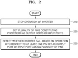
- FIG. 2 is a flowchart showing an example of a method of detecting whether an inverter fails, according to one aspect.
- the method shown in FIG. 2 may include operations processed in time series in the processor 110 shown in FIG. 1 . Therefore, the foregoing description of the processor 110, even though being omitted below, may be applied to the method shown in FIG. 2 .
- the processor 110 may stop the operation of the inverter.
- the processor 110 may stop the operation of the inverter.
- a signal requesting detection of a failure of the inverter hereinafter referred to as a 'failure detection request signal'
- the processor 110 may stop the operation of the inverter.
- An example in which the processor 110 stops the operation of the inverter will be described later with reference to operations 310 and 320 of FIG. 3 .
- the processor 110 may set a plurality of pins 111 constituting the processor 110 as output ports or input ports.
- the processor 110 may set at least one pin among the plurality of pins 111 constituting the processor 110 as an output port or an input port to check a digital input/output error.
- An example in which the processor 110 sets a pin as an output port or an input port will be described later with reference to operation 330 of FIG. 3 .
- the processor 110 may detect whether the inverter fails, based on an operation with respect to the at least one pin among the plurality of pins 111 set as the output ports or the input ports.
- the processor 110 may identify an operation with respect to at least one pin set as an output port. For example, the processor 110 may generate an output signal by setting the at least one pin as the output port. The processor 110 may convert the pin set as the output port to an input port and receive an input signal corresponding to the output signal. Then, the processor 110 may determine whether an error has occurred in the at least one pin, by comparing the output signal with the input signal.
- the processor 110 may compare the output signal generated from the at least one pin with an input signal, received from the at least one pin due to a ground short, to determine whether an error has occurred in the at least one pin. As another example, the processor 110 may compare the output signal generated from the at least one pin with an input signal, received from the at least one pin due to a supply voltage short, to determine whether an error has occurred in the at least one pin.
- the processor 110 may identify an operation with respect to at least one pin set as an input port. For example, the processor 110 may set the at least one pin as the input port and determine whether an error has occurred in the at least one pin, based on a signal received from the termination device 130 of the processor 110. Specifically, the processor 110 may identify a normal range of a signal strength corresponding to the termination device 130, and the processor 110 may receive a signal from the termination device 130. The processor 110 may determine whether an error has occurred in the at least one pin, based on whether the strength of the received signal is within the normal range.
- processor 110 detects whether the inverter fails, based on the operation with respect to the pin, will be described later with reference to operations 340 to 370 of FIG. 3 .
- FIG. 3 is a flowchart showing an example in which a processor detects whether an inverter fails, according to one aspect.
- the processor 110 may identify a failure detection request signal of the inverter.
- the failure detection request signal may be generated according to a preset detection cycle or may be input from a manager of the inverter.
- the processor 110 may perform operation 320.
- the processor 110 may continuously monitor whether the failure detection request signal is identified.
- the processor 110 may stop an operation of the inverter.
- the inverter may be connected to the processor 110 as a separate device, or the processor 110 may be included in the inverter.
- the processor 110 may set at least one pin among the plurality of pins 111 constituting the processor 110 as an output port or an input port to check a digital input/output error.
- the processor 110 may perform operation 340.
- the processor 110 may perform operation 350.
- the processor 110 may identify the operation with respect to the at least one pin set as the output port and perform operation 360.
- the processor 110 identifies the operation with respect to the at least one pin set as the output port.
- FIG. 4 is a flowchart showing an example to check an error by setting a pin of a processor as an output port, according to one aspect.
- the processor 110 may generate an output signal that may be output from the output port.
- the processor 110 may convert the pins 111 set as output ports into input ports.
- the processor 110 may determine whether the output signal output from the pin is the same as the input signal input to the pin. For example, the processor 110 may output an output signal through a pin connected to the gate driver 120 among the pins 111 set as the output ports. The processor 110 may change a pin set as an output port to an input port. Then, the processor 110 may receive a signal corresponding to the output signal as an input signal through the pin changed to the input port and identify the received signal.
- the processor 110 may identify, as an input signal, a signal before the output signal is output and discharged. For example, a time when an output signal is output may be shorter than a time when a pin set as an output port is changed to an input port. In addition, after the output signal is output, a time until the output signal is erased due to the pin set as the output port being changed to the input port may be longer than a time in which an error is checked.
- the processor 110 may determine that the corresponding pin operates normally, in operation 440.
- the processor 110 may determine that an error has occurred in the corresponding pin, in operation 450.
- the processor 110 may detect a short that occurs while checking an error of the pin.
- examples in which the processor 110 detects a short will be described with reference to FIGS. 5 and 6 .
- FIGS. 5 and 6 are diagrams to describe examples of a method of causing a short, according to one aspect.
- the gate driver 120 connected to the processor 110 may be connected to a ground 140.
- the processor 110 may identify a case where an abnormal input signal is transmitted to at least one pin of the processor 110 due to occurrence of a ground short to determine whether an error has occurred in the corresponding pin.
- a signal (e.g., 0 V) output from the ground 140 due to the ground short may be input to the pin set as the input pin.
- the processor 110 may determine that the corresponding pin operates normally even in a situation where the ground short occurs. Alternatively, when the input signal is not 0 V, the processor 110 may determine that an error has occurred in the corresponding pin.
- a supply voltage may be connected to the gate driver 120 connected to the processor 110.
- the processor 110 may identify a case where an abnormal input signal is transmitted to at least one pin due to occurrence of a supply voltage short to determine whether an error has occurred in the corresponding pin.
- a signal (e.g., 5 V) output from the supply voltage due to the supply voltage short may be input to the pin set as the input pin.
- the processor 110 may determine that the corresponding pin operates normally even in a situation where the supply voltage short occurs. Alternatively, when the input signal is not 5 V, the processor 110 may determine that an error has occurred in the corresponding pin.
- the processor 110 may determine whether all pins 111 constituting the processor 110 have been checked for a failure. When operation states of all the pins 111 are identified, the processor 110 may perform operation 370. Alternatively, when the operation states of all the pins 111 are not identified, the processor 110 may perform operations 330 and 340 again. At this time, the processor 110 may identify the operation states of all the pins 111 and an operation state of a pin connected to the gate driver 120.
- the processor 110 may determine whether there is an error in at least one pin provided in the processor 110, based on a result of identifying an operation state of a pin set as an output port. Based on the determination, the processor 110 may determine whether the inverter fails.
- the processor 110 may determine that the failure has occurred in the inverter.
- the processor 110 may identify an operation with respect to a pin set as an input port. Then, the processor 110 may perform operation 360.
- the processor 110 may identify an operation with respect to a pin set as an input port. Then, the processor 110 may perform operation 360.
- the processor 110 identifies the operation with respect to the pin set as the input port.
- FIG. 7 is a flowchart showing an example to check an error by setting a pin of a processor as an input port, according to one aspect.
- the processor 110 may identify a normal range of a signal strength corresponding to the termination device 130. In operation 720, the processor 110 may receive a signal from the termination device 130 through the gate driver 120.
- the processor 110 may determine whether the strength of the signal received from the termination device 130 is within the normal range.
- the processor 110 may perform operation 740.
- the processor 110 may determine that the corresponding pin operates normally when the strength of the received signal is within the normal range.
- the processor 110 may perform operation 750.
- the processor 110 may determine that the corresponding pin does not operate normally when the strength of the received signal is not within the normal range.
- the processor 110 may determine whether all the pins 111 constituting the processor 110 have been checked for a failure.
- the processor 110 may perform operations 330 and 350 again.
- the processor 110 may perform operation 370.
- the processor 110 may determine whether there is an error in the at least one pin, based on a result of identifying an operation state of a pin set as an input port. For example, the processor 110 may identify the operation states of all the pins 111 and an operation state of a pin connected to the termination device 130.
- the processor 110 may determine whether the inverter fails.
- the processor 110 may check a digital input/output error occurring in the processor 110 even when the inverter is stopped, without addition of a separate circuit. Therefore, a failure of the inverter may be easily and accurately checked before power is supplied to the inverter.
- the above-described method may be written as a program executable on a computer, and may be implemented in a general-purpose digital computer that operates the program using a computer-readable recording medium. Additionally, a data structure used in the above-described method may be recorded on a computer-readable recording medium through various means.
- the computer-readable recording medium may include a storage medium such as a magnetic storage medium (e.g., ROM, RAM, USB, floppy disk, hard disk, etc.) and an optical read medium (e.g., CD-ROM, DVD, etc.).
Landscapes
- Physics & Mathematics (AREA)
- General Physics & Mathematics (AREA)
- Engineering & Computer Science (AREA)
- General Engineering & Computer Science (AREA)
- Power Engineering (AREA)
- Inverter Devices (AREA)
- Measurement Of Current Or Voltage (AREA)
- Tests Of Electronic Circuits (AREA)
- Test And Diagnosis Of Digital Computers (AREA)
Abstract
Description
- The present disclosure relates to a method and apparatus for detecting whether an inverter fails.
- Inverters are devices that convert direct current into alternating current, and are used in industrial fields using various electronic devices such as not only motor-driven drives, uninterruptible power supply (UPS), active power filters, etc., but also renewable energy systems, hybrid vehicles, etc.
- Although inverter design and control technology is advancing, many types of unexpected inverter failures frequently occur. Failures of an inverter may include digital input/output errors of a processor connected to or included in the inverter. In this case, the digital input/output errors may affect an operation of the inverter. Hence, to increase the reliability of the inverter and eliminate adverse effects caused by a failure of the inverter, detection of the digital input/output errors is required.
- The present disclosure provides a method and apparatus for detecting whether an inverter fails. The present disclosure also provides a computer-readable recording medium having recorded thereon a program for executing the method on a computer. The technical problems of the present disclosure are not limited to the aforementioned technical problems, and other technical problems may exist.
- According to one aspect, a method of detecting whether an inverter fails includes stopping an operation of the inverter, setting a plurality of pins constituting a processor as output ports or input ports, and detecting whether the inverter fails, based on an operation with respect to at least one pin set as an output port or an input port among the plurality of pins.
- A computer-readable recording medium according to another aspect includes a recording medium having recorded thereon a program for executing the above-described method on a computer.
- According to another aspect, a processor is configured to stop an operation of the inverter, set a plurality of pins constituting a processor as output ports or input ports, and detect whether the inverter fails, based on an operation with respect to at least one pin set as an output port or an input port among the plurality of pins.
- Without addition of a separate circuit, digital input/output errors occurring in a processor may be checked while the inverter is stopped. Therefore, a failure of the inverter may be easily and accurately checked before power is supplied to the inverter.
-
-
FIG. 1 is a diagram illustrating an example of a processor and elements connected to the processor according to one aspect. -
FIG. 2 is a flowchart showing an example of a method of detecting whether an inverter fails, according to one aspect. -
FIG. 3 is a flowchart showing an example in which a processor detects whether an inverter fails, according to one aspect. -
FIG. 4 is a flowchart showing an example to check an error by setting a pin of a processor as an output port, according to one aspect. -
FIGS. 5 and6 are diagrams to describe examples of a method of causing a short, according to one aspect. -
FIG. 7 is a flowchart showing an example to check an error by setting a pin of a processor as an input port, according to one aspect. - According to one aspect, a method of detecting whether an inverter fails includes stopping an operation of the inverter, setting a plurality of pins constituting a processor as output ports or input ports, and detecting whether the inverter fails, based on an operation with respect to at least one pin set as an output port or an input port among the plurality of pins.
- Although terms used in embodiments are selected with general terms popularly used at present as much as possible, the terms may vary according to the intention of those of ordinary skill in the art, judicial precedents, or introduction of new technology. In addition, in a specific case, the applicant voluntarily may select terms, and in this case, the meaning of the terms may be disclosed in detail in a corresponding description part. Thus, the terms used herein should be defined not by the simple names of the terms but by the meaning of the terms and the contents throughout the present specification.
- Throughout the entirety of the specification, when a certain part "includes" a certain component, it may mean that the component may further include other components rather than exclude other components, unless specially described to the contrary.
- In addition, terms, such as "first", "second", etc., used herein, may be used to describe various components, but the components should not be limited by the terms. These terms are used to distinguish one component from another component.
- Hereinafter, preferred embodiments of the present disclosure will be described in detail with reference to the attached drawings. The detailed description set forth below in conjunction with the accompanying drawings is intended to describe example embodiments of the present disclosure and is not intended to represent the only embodiment in which the present disclosure may be practiced. In the drawings, to clearly describe the present disclosure, parts unrelated to the description may be omitted, and the same reference numerals may be used for the same or similar components throughout the specification.
-
FIG. 1 is a diagram illustrating an example of a processor and elements connected to the processor according to one aspect. - Referring to
FIG. 1 , aprocessor 110 may be connected to at least onetermination device 130 through agate driver 120. For example, thetermination device 130 may be, but not limited to, a field effect transistor (FET). Theprocessor 110 may also includepins 111 by which and theprocessor 110 and thegate driver 120 may be connected to each other. - For example, at least one of the
processor 110, thegate driver 120, and thetermination device 130 may be included in the inverter. Alternatively, at least one of theprocessor 110, thegate driver 120, and thetermination device 130 may be connected to the inverter. - The inverter may be included in a power generation device or system using renewable energy (e.g., solar heat, solar energy, biomass, wind power, small hydro, geothermal heat, marine energy, waste energy, etc.). For example, for a solar energy generation device or system, the inverter may be a micro inverter or string inverter connected to at least one photovoltaic (PV) module. When the inverter is a string inverter, an optimizer may be connected to the PV module.
- However, a device or system including the inverter is not limited to the example described above. For example, as long as a device needs to convert power from direct current to alternating current, or from alternating current to direct current, the inverter may be included in the device or in the system without a limitation. For example, any processor included in a device or system that needs to convert power may be the
processor 110 without a limitation. - The
processor 110 may process an instruction of a computer program by performing basic arithmetic, logic, and input/output operations. Here, the instruction may be provided from an internal memory of theprocessor 110 or from an external device. Theprocessor 110 may generally control operations of other components included in the inverter. - For example, the
processor 110 may be implemented as an array of multiple logic gates, or may be implemented as a combination of a general-purpose microprocessor and a memory storing a program executable on the microprocessor. For example, theprocessor 110 may include a general-purpose processor, a central processing unit (CPU), a graphics processing unit (GPU), a neural network processing unit (NPU), a microprocessor, a digital signal processor (DSP), a controller, a microcontroller, a state machine, etc. In some environments, theprocessor 110 may include an application specific integrated circuit (ASIC), a programmable logic device (PLD), a field programmable gate array (FPGA), etc. For example, theprocessor 110 may refer to a combination of a DSP and a microprocessor, a combination of a plurality of microprocessors, a combination of one or more microprocessors combined with a DSP core, or a combination of processing devices such as any combination of other such components. - Meanwhile, the
processor 110 may include a memory, although not shown inFIG. 1 . For example, the memory may include any non-transitory computer-readable recording medium. - As an example, the memory may include a permanent mass storage device such as random access memory (RAM), read only memory (ROM), disk drive, solid state drive (SSD), flash memory, etc. As another example, a non-perishable mass storage device such as ROM, SSD, flash memory, disk drives, etc., may be a separate permanent storage device distinct from the memory. An operating system (OS) and at least one program code (e.g., a code for the
processor 110 to perform operations to be described later with reference toFIGS. 2 to 7 ) may be stored in the memory. - These software components may be loaded from a computer-readable recording medium separate from the memory. This separate computer-readable recording medium may be a recording medium that may be directly connected to a computer, and include a computer-readable recording medium, for example, floppy drive, disk, tape, DVD/CD-ROM drive, memory card, etc. Alternatively, software components may be loaded onto the memory through a communication device rather than a computer-readable recording medium. For example, at least one program may be loaded onto the memory based on a computer program (e.g., a computer program for the
processor 110 to perform operations to be described later with reference toFIGS. 2 to 7 ) installed by files provided through the communication device by developers or a file distribution system that distributes an installation file of an application. - Digital input/output errors of the
processor 110 may affect an operation of the inverter. To prevent the digital input/output errors of theprocessor 110, theprocessor 110 needs to satisfy functional safety (UL991) standard certification. In particular, it should be determined whether a function of theprocessor 110 satisfies digital input/output diagnostic items among internal safety diagnostic items. Here, a digital input/output diagnostic item may refer to an item for diagnosing whether thepins 111 included in theprocessor 110 properly perform input and output functions. - In general, when an error occurs during an operation of the inverter, it may be determined whether a digital input/output error occurs in the
processor 110, based on a sensing value output from or input to the inverter. However, in the above-described method, it is difficult to determine in which of thepins 111 the error has occurred. In addition, when using the above-described method, a separate circuit needs to be added to theprocessor 110 to identify a type of the pin in which the error has occurred. To determine whether the digital input/output error of theprocessor 110 has occurred, the inverter has to operate. - The
processor 110 according to one embodiment may check a digital input/output error occurring in theprocessor 110 even when the inverter is stopped, without addition of a separate circuit. Therefore, a failure of the inverter may be easily and accurately checked before power is supplied to the inverter. -
FIG. 2 is a flowchart showing an example of a method of detecting whether an inverter fails, according to one aspect. - The method shown in
FIG. 2 may include operations processed in time series in theprocessor 110 shown inFIG. 1 . Therefore, the foregoing description of theprocessor 110, even though being omitted below, may be applied to the method shown inFIG. 2 . - In
operation 210, theprocessor 110 may stop the operation of the inverter. - For example, when a signal requesting detection of a failure of the inverter (hereinafter referred to as a 'failure detection request signal') is identified, the
processor 110 may stop the operation of the inverter. An example in which theprocessor 110 stops the operation of the inverter will be described later with reference tooperations FIG. 3 . - In
operation 220, theprocessor 110 may set a plurality ofpins 111 constituting theprocessor 110 as output ports or input ports. - For example, the
processor 110 may set at least one pin among the plurality ofpins 111 constituting theprocessor 110 as an output port or an input port to check a digital input/output error. An example in which theprocessor 110 sets a pin as an output port or an input port will be described later with reference tooperation 330 ofFIG. 3 . - In
operation 230, theprocessor 110 may detect whether the inverter fails, based on an operation with respect to the at least one pin among the plurality ofpins 111 set as the output ports or the input ports. - The
processor 110 may identify an operation with respect to at least one pin set as an output port. For example, theprocessor 110 may generate an output signal by setting the at least one pin as the output port. Theprocessor 110 may convert the pin set as the output port to an input port and receive an input signal corresponding to the output signal. Then, theprocessor 110 may determine whether an error has occurred in the at least one pin, by comparing the output signal with the input signal. - As an example, the
processor 110 may compare the output signal generated from the at least one pin with an input signal, received from the at least one pin due to a ground short, to determine whether an error has occurred in the at least one pin. As another example, theprocessor 110 may compare the output signal generated from the at least one pin with an input signal, received from the at least one pin due to a supply voltage short, to determine whether an error has occurred in the at least one pin. - The
processor 110 may identify an operation with respect to at least one pin set as an input port. For example, theprocessor 110 may set the at least one pin as the input port and determine whether an error has occurred in the at least one pin, based on a signal received from thetermination device 130 of theprocessor 110. Specifically, theprocessor 110 may identify a normal range of a signal strength corresponding to thetermination device 130, and theprocessor 110 may receive a signal from thetermination device 130. Theprocessor 110 may determine whether an error has occurred in the at least one pin, based on whether the strength of the received signal is within the normal range. - An example in which the
processor 110 detects whether the inverter fails, based on the operation with respect to the pin, will be described later with reference tooperations 340 to 370 ofFIG. 3 . -
FIG. 3 is a flowchart showing an example in which a processor detects whether an inverter fails, according to one aspect. - In
operation 310, theprocessor 110 may identify a failure detection request signal of the inverter. - For example, the failure detection request signal may be generated according to a preset detection cycle or may be input from a manager of the inverter. When the failure detection request signal is identified, the
processor 110 may performoperation 320. When the failure detection request signal is not identified, theprocessor 110 may continuously monitor whether the failure detection request signal is identified. - In
operation 320, theprocessor 110 may stop an operation of the inverter. For example, the inverter may be connected to theprocessor 110 as a separate device, or theprocessor 110 may be included in the inverter. - In
operation 330, theprocessor 110 may set at least one pin among the plurality ofpins 111 constituting theprocessor 110 as an output port or an input port to check a digital input/output error. When theprocessor 110 sets the at least one pin as the output port, theprocessor 110 may performoperation 340. When theprocessor 110 sets the at least one pin as the input port, theprocessor 110 may performoperation 350. - In
operation 340, theprocessor 110 may identify the operation with respect to the at least one pin set as the output port and performoperation 360. Hereinbelow, an example in which theprocessor 110 identifies the operation with respect to the at least one pin set as the output port will be described with reference toFIG. 4 . -
FIG. 4 is a flowchart showing an example to check an error by setting a pin of a processor as an output port, according to one aspect. - In
operation 410, theprocessor 110 may generate an output signal that may be output from the output port. Inoperation 420, theprocessor 110 may convert thepins 111 set as output ports into input ports. - In
operation 430, theprocessor 110 may determine whether the output signal output from the pin is the same as the input signal input to the pin. For example, theprocessor 110 may output an output signal through a pin connected to thegate driver 120 among thepins 111 set as the output ports. Theprocessor 110 may change a pin set as an output port to an input port. Then, theprocessor 110 may receive a signal corresponding to the output signal as an input signal through the pin changed to the input port and identify the received signal. - Through the above-described process, the
processor 110 may identify, as an input signal, a signal before the output signal is output and discharged. For example, a time when an output signal is output may be shorter than a time when a pin set as an output port is changed to an input port. In addition, after the output signal is output, a time until the output signal is erased due to the pin set as the output port being changed to the input port may be longer than a time in which an error is checked. - When the output signal and the input signal are the same as each other, the
processor 110 may determine that the corresponding pin operates normally, inoperation 440. When the output signal and the input signal are different from each other, theprocessor 110 may determine that an error has occurred in the corresponding pin, inoperation 450. - For example, the
processor 110 may detect a short that occurs while checking an error of the pin. Hereinafter, examples in which theprocessor 110 detects a short will be described with reference toFIGS. 5 and6 . -
FIGS. 5 and6 are diagrams to describe examples of a method of causing a short, according to one aspect. - Referring to
FIG. 5 , thegate driver 120 connected to theprocessor 110 may be connected to aground 140. Theprocessor 110 may identify a case where an abnormal input signal is transmitted to at least one pin of theprocessor 110 due to occurrence of a ground short to determine whether an error has occurred in the corresponding pin. - When the ground short occurs in the
ground 140 connected to thegate driver 120, a signal (e.g., 0 V) output from theground 140 due to the ground short may be input to the pin set as the input pin. When the input signal input from the input pin (for example, the input signal due to the ground short) is 0 V, theprocessor 110 may determine that the corresponding pin operates normally even in a situation where the ground short occurs. Alternatively, when the input signal is not 0 V, theprocessor 110 may determine that an error has occurred in the corresponding pin. - Referring to
FIG. 6 , a supply voltage may be connected to thegate driver 120 connected to theprocessor 110. Theprocessor 110 may identify a case where an abnormal input signal is transmitted to at least one pin due to occurrence of a supply voltage short to determine whether an error has occurred in the corresponding pin. - When the supply voltage short occurs in the supply voltage connected to the
gate driver 120, a signal (e.g., 5 V) output from the supply voltage due to the supply voltage short may be input to the pin set as the input pin. When the input signal input from the input pin (for example, the input signal due to the supply voltage short) is 5 V, theprocessor 110 may determine that the corresponding pin operates normally even in a situation where the supply voltage short occurs. Alternatively, when the input signal is not 5 V, theprocessor 110 may determine that an error has occurred in the corresponding pin. - Referring back to
FIG. 3 , inoperation 360, theprocessor 110 may determine whether all pins 111 constituting theprocessor 110 have been checked for a failure. When operation states of all thepins 111 are identified, theprocessor 110 may performoperation 370. Alternatively, when the operation states of all thepins 111 are not identified, theprocessor 110 may performoperations processor 110 may identify the operation states of all thepins 111 and an operation state of a pin connected to thegate driver 120. - In
operation 370, theprocessor 110 may determine whether there is an error in at least one pin provided in theprocessor 110, based on a result of identifying an operation state of a pin set as an output port. Based on the determination, theprocessor 110 may determine whether the inverter fails. - For example, when it is determined that the error has occurred in the at least one pin among all the
pins 111, theprocessor 110 may determine that the failure has occurred in the inverter. - In
operation 350, theprocessor 110 may identify an operation with respect to a pin set as an input port. Then, theprocessor 110 may performoperation 360. Hereinbelow, an example in which theprocessor 110 identifies the operation with respect to the pin set as the input port will be described with reference toFIG. 7 . -
FIG. 7 is a flowchart showing an example to check an error by setting a pin of a processor as an input port, according to one aspect. - In
operation 710, theprocessor 110 may identify a normal range of a signal strength corresponding to thetermination device 130. Inoperation 720, theprocessor 110 may receive a signal from thetermination device 130 through thegate driver 120. - In
operation 730, theprocessor 110 may determine whether the strength of the signal received from thetermination device 130 is within the normal range. - When the strength of the received signal is within the normal range, the
processor 110 may performoperation 740. Inoperation 740, theprocessor 110 may determine that the corresponding pin operates normally when the strength of the received signal is within the normal range. - When the strength of the received signal is not within the normal range, the
processor 110 may performoperation 750. Inoperation 750, theprocessor 110 may determine that the corresponding pin does not operate normally when the strength of the received signal is not within the normal range. - Referring back to
FIG. 3 , inoperation 360, theprocessor 110 may determine whether all thepins 111 constituting theprocessor 110 have been checked for a failure. - When the check for the failure of all the
pins 111 is not completed, theprocessor 110 may performoperations pins 111 is completed, theprocessor 110 may performoperation 370. - In
operation 370, theprocessor 110 may determine whether there is an error in the at least one pin, based on a result of identifying an operation state of a pin set as an input port. For example, theprocessor 110 may identify the operation states of all thepins 111 and an operation state of a pin connected to thetermination device 130. - Based on the determination, the
processor 110 may determine whether the inverter fails. - According to the foregoing description, the
processor 110 according to one embodiment may check a digital input/output error occurring in theprocessor 110 even when the inverter is stopped, without addition of a separate circuit. Therefore, a failure of the inverter may be easily and accurately checked before power is supplied to the inverter. - Meanwhile, the above-described method may be written as a program executable on a computer, and may be implemented in a general-purpose digital computer that operates the program using a computer-readable recording medium. Additionally, a data structure used in the above-described method may be recorded on a computer-readable recording medium through various means. The computer-readable recording medium may include a storage medium such as a magnetic storage medium (e.g., ROM, RAM, USB, floppy disk, hard disk, etc.) and an optical read medium (e.g., CD-ROM, DVD, etc.).
- The embodiments of the present disclosure set forth herein and in the drawings are merely provided as specific examples to easily describe the technical content of the present disclosure and to facilitate understanding of the present disclosure, and are not intended to limit the scope of the present disclosure. Therefore, the scope of the present disclosure should be construed as including all changes or modified forms derived based on the technical spirit of the present disclosure as well as the embodiments disclosed herein.
Claims (17)
- A method of detecting whether an inverter fails, the method comprising:stopping an operation of the inverter;setting a plurality of pins constituting a processor as output ports or input ports; anddetecting whether the inverter fails, based on an operation with respect to at least one pin set as an output port or an input port among the plurality of pins.
- The method of claim 1, wherein the detecting comprises identifying the operation with respect to the at least one pin set as the output port.
- The method of claim 2, wherein the detecting comprises:setting the at least one pin as the output port to generate an output signal;converting the at least one pin set as the output port into an input port to receive an input signal corresponding to the output signal; andcomparing the output signal with the input signal to determine whether an error has occurred in the at least one pin.
- The method of claim 3, wherein the detecting comprises detecting whether an error has occurred in the at least one pin by comparing an output signal generated from the at least one pin with an input signal received from the at least one pin due to a ground short.
- The method of claim 4, wherein the detecting comprises detecting whether an error has occurred in the at least one pin by comparing the output signal generated from the at least one pin with an input signal received from the at least one pin due to a supply voltage short.
- The method of claim 1, wherein the detecting comprises identifying the operation with respect to the at least one pin set as the input port.
- The method of claim 6, wherein the detecting comprises:setting the at least one pin as the input port; anddetermining whether an error has occurred in the at least one pin, based on a signal received from a device connected to a terminal of the processor.
- The method of claim 7, wherein the detecting comprises:identifying a normal range of a signal strength corresponding to the device connected to the terminal;receiving a signal from the device connected to the terminal; anddetermining whether an error has occurred in the at least one pin, based on whether a strength of the received signal is within the normal range.
- A computer-readable recording medium having recorded thereon a program for causing a computer to execute the method of claim 1.
- A processor configured to:stop an operation of an inverter;set a plurality of pins constituting a processor as output ports or input ports; anddetect whether the inverter fails, based on an operation with respect to at least one pin set as an output port or an input port among the plurality of pins.
- The processor of claim 10, wherein the processor is further configured to identify the operation with respect to the at least one pin set as the output port.
- The processor of claim 11, wherein the processor is further configured to:set the at least one pin as the output port to generate an output signal;convert the at least one pin set as the output port into an input port to receive an input signal corresponding to the output signal; andcompare the output signal with the input signal to determine whether an error has occurred in the at least one pin.
- The processor of claim 12, wherein the processor is further configured to detect whether an error has occurred in the at least one pin by comparing an output signal generated from the at least one pin with an input signal received from the at least one pin due to a ground short.
- The processor of claim 13, wherein the processor is further configured to detect whether an error has occurred in the at least one pin by comparing the output signal generated from the at least one pin with an input signal received from the at least one pin due to a supply voltage short.
- The processor of claim 10, wherein the processor is further configured to identify the operation with respect to the at least one pin set as the input port.
- The processor of claim 15, wherein the processor is further configured to set the at least one pin as the input port and determine whether an error has occurred in the at least one pin, based on a signal received from a device connected to a terminal of the processor.
- The processor of claim 16, wherein the processor is further configured to:identify a normal range of a signal strength corresponding to the device connected to the terminal;receive a signal from the device connected to the terminal; anddetermine whether an error has occurred in the at least one pin, based on whether a strength of the received signal is within the normal range.
Applications Claiming Priority (2)
| Application Number | Priority Date | Filing Date | Title |
|---|---|---|---|
| KR1020230040400A KR102866330B1 (en) | 2023-03-28 | 2023-03-28 | Method and Apparatus for Fault Detecting of Inverter |
| PCT/KR2024/003905 WO2024205245A1 (en) | 2023-03-28 | 2024-03-28 | Method and device for detecting whether failure has occurred in inverter |
Publications (2)
| Publication Number | Publication Date |
|---|---|
| EP4502631A1 true EP4502631A1 (en) | 2025-02-05 |
| EP4502631A4 EP4502631A4 (en) | 2025-10-15 |
Family
ID=92906394
Family Applications (1)
| Application Number | Title | Priority Date | Filing Date |
|---|---|---|---|
| EP24781235.7A Pending EP4502631A4 (en) | 2023-03-28 | 2024-03-28 | METHOD AND DEVICE FOR DETECTING WHETHER A FAILURE HAS OCCURRED IN AN INVERTER |
Country Status (5)
| Country | Link |
|---|---|
| US (1) | US20250264549A1 (en) |
| EP (1) | EP4502631A4 (en) |
| JP (1) | JP2025538232A (en) |
| KR (1) | KR102866330B1 (en) |
| WO (1) | WO2024205245A1 (en) |
Family Cites Families (6)
| Publication number | Priority date | Publication date | Assignee | Title |
|---|---|---|---|---|
| KR101653221B1 (en) * | 2014-06-10 | 2016-09-01 | (주) 모터에이드 | Inverter and method for contolling the same |
| KR101790134B1 (en) * | 2016-05-27 | 2017-10-25 | 엘지전자 주식회사 | Error diagnosis method for inverter |
| US9899953B2 (en) * | 2016-06-27 | 2018-02-20 | Rockwell Automation Technologies, Inc. | Method and apparatus for detecting ground faults in inverter outputs on a shared DC bus |
| KR101887899B1 (en) * | 2016-09-12 | 2018-08-13 | 현대오트론 주식회사 | Apparatus and method for detecting short circuit among output pins out and among driver ics |
| KR20190001445A (en) * | 2017-06-27 | 2019-01-04 | 엘에스산전 주식회사 | Method for diagnosing condition of inverter |
| CN110888085A (en) * | 2019-11-29 | 2020-03-17 | 华为数字技术(苏州)有限公司 | Inverter short circuit detection method and device and inverter |
-
2023
- 2023-03-28 KR KR1020230040400A patent/KR102866330B1/en active Active
-
2024
- 2024-03-28 JP JP2025528550A patent/JP2025538232A/en active Pending
- 2024-03-28 US US18/858,456 patent/US20250264549A1/en active Pending
- 2024-03-28 WO PCT/KR2024/003905 patent/WO2024205245A1/en not_active Ceased
- 2024-03-28 EP EP24781235.7A patent/EP4502631A4/en active Pending
Also Published As
| Publication number | Publication date |
|---|---|
| KR102866330B1 (en) | 2025-09-30 |
| KR20240145666A (en) | 2024-10-07 |
| EP4502631A4 (en) | 2025-10-15 |
| WO2024205245A1 (en) | 2024-10-03 |
| JP2025538232A (en) | 2025-11-26 |
| US20250264549A1 (en) | 2025-08-21 |
Similar Documents
| Publication | Publication Date | Title |
|---|---|---|
| CN107193713B (en) | FPGA and method for realizing mainboard management control | |
| US20120221884A1 (en) | Error management across hardware and software layers | |
| Drozd et al. | Checkability of the digital components in safety-critical systems: problems and solutions | |
| JPWO2018221136A1 (en) | Abnormality determination device, abnormality determination method, and abnormality determination program | |
| CN116746064A (en) | Lockstep comparators and related methods | |
| CN112462920B (en) | Method, device, server and storage medium for power control | |
| CN103257922B (en) | A kind of method of quick test BIOS and OS interface code reliability | |
| KR20200062443A (en) | Method for self diagnosis of ram error detection logic in powertrain ecu system and apparatus thereof | |
| US9158646B2 (en) | Abnormal information output system for a computer system | |
| JP2005135407A (en) | System and method for testing component of computer system by using voltage margining | |
| CN118936604A (en) | A self-checking and positioning method, device, medium and product for abnormal power consumption of water meter | |
| EP4502631A1 (en) | Method and device for detecting whether failure has occurred in inverter | |
| CN111858121A (en) | Multi-mode redundancy configuration system for processor | |
| Leaphart et al. | Survey of software failsafe techniques for safety-critical automotive applications | |
| CN111429962A (en) | Method and device for periodically performing BIST test on memory, computer equipment and storage medium | |
| US9256504B2 (en) | Semiconductor integrated circuit including a state machine | |
| US20220107866A1 (en) | Fast memory ecc error correction | |
| CN113394963B (en) | A PFC circuit detection method and device and readable storage medium | |
| CN119127720A (en) | A BAMS equipment automated testing method and device | |
| JP2021005379A (en) | Method for detecting deep learning chip, device, electronic apparatus, and computer storage medium | |
| US20190086451A1 (en) | Method and system for measuring power-on reset time | |
| CN115904793A (en) | Memory unloading method, system and chip based on multi-core heterogeneous system | |
| CN104834535A (en) | SOC (System On Chip) chip system and power on method thereof | |
| CN116541211A (en) | Keyboard controller style interface fault redundancy method and device | |
| CN120596322B (en) | Fault injection testing method, device, computer equipment and storage medium |
Legal Events
| Date | Code | Title | Description |
|---|---|---|---|
| STAA | Information on the status of an ep patent application or granted ep patent |
Free format text: STATUS: THE INTERNATIONAL PUBLICATION HAS BEEN MADE |
|
| PUAI | Public reference made under article 153(3) epc to a published international application that has entered the european phase |
Free format text: ORIGINAL CODE: 0009012 |
|
| STAA | Information on the status of an ep patent application or granted ep patent |
Free format text: STATUS: REQUEST FOR EXAMINATION WAS MADE |
|
| 17P | Request for examination filed |
Effective date: 20241030 |
|
| AK | Designated contracting states |
Kind code of ref document: A1 Designated state(s): AL AT BE BG CH CY CZ DE DK EE ES FI FR GB GR HR HU IE IS IT LI LT LU LV MC ME MK MT NL NO PL PT RO RS SE SI SK SM TR |
|
| STAA | Information on the status of an ep patent application or granted ep patent |
Free format text: STATUS: EXAMINATION IS IN PROGRESS |
|
| A4 | Supplementary search report drawn up and despatched |
Effective date: 20250912 |
|
| RIC1 | Information provided on ipc code assigned before grant |
Ipc: G01R 31/317 20060101AFI20250908BHEP Ipc: G01R 31/3183 20060101ALI20250908BHEP Ipc: G01R 31/40 20200101ALI20250908BHEP Ipc: G01R 19/25 20060101ALI20250908BHEP Ipc: G01R 31/52 20200101ALI20250908BHEP Ipc: G01R 19/165 20060101ALI20250908BHEP Ipc: G01R 31/42 20060101ALI20250908BHEP |
|
| 17Q | First examination report despatched |
Effective date: 20250924 |