EP4498518A1 - Wellenleiterantennenanordnung, radar, endgerät und herstellungsverfahren für wellenleiterantennenanordnung - Google Patents
Wellenleiterantennenanordnung, radar, endgerät und herstellungsverfahren für wellenleiterantennenanordnung Download PDFInfo
- Publication number
- EP4498518A1 EP4498518A1 EP23778208.1A EP23778208A EP4498518A1 EP 4498518 A1 EP4498518 A1 EP 4498518A1 EP 23778208 A EP23778208 A EP 23778208A EP 4498518 A1 EP4498518 A1 EP 4498518A1
- Authority
- EP
- European Patent Office
- Prior art keywords
- substrate
- waveguide
- hole
- board surface
- antenna assembly
- Prior art date
- Legal status (The legal status is an assumption and is not a legal conclusion. Google has not performed a legal analysis and makes no representation as to the accuracy of the status listed.)
- Pending
Links
Images





Classifications
-
- H—ELECTRICITY
- H01—ELECTRIC ELEMENTS
- H01Q—ANTENNAS, i.e. RADIO AERIALS
- H01Q1/00—Details of, or arrangements associated with, antennas
- H01Q1/36—Structural form of radiating elements, e.g. cone, spiral, umbrella; Particular materials used therewith
-
- H—ELECTRICITY
- H01—ELECTRIC ELEMENTS
- H01P—WAVEGUIDES; RESONATORS, LINES, OR OTHER DEVICES OF THE WAVEGUIDE TYPE
- H01P5/00—Coupling devices of the waveguide type
- H01P5/08—Coupling devices of the waveguide type for linking dissimilar lines or devices
- H01P5/10—Coupling devices of the waveguide type for linking dissimilar lines or devices for coupling balanced lines or devices with unbalanced lines or devices
- H01P5/107—Hollow-waveguide/strip-line transitions
-
- H—ELECTRICITY
- H01—ELECTRIC ELEMENTS
- H01Q—ANTENNAS, i.e. RADIO AERIALS
- H01Q1/00—Details of, or arrangements associated with, antennas
- H01Q1/002—Protection against seismic waves, thermal radiation or other disturbances, e.g. nuclear explosion; Arrangements for improving the power handling capability of an antenna
-
- H—ELECTRICITY
- H01—ELECTRIC ELEMENTS
- H01Q—ANTENNAS, i.e. RADIO AERIALS
- H01Q1/00—Details of, or arrangements associated with, antennas
- H01Q1/12—Supports; Mounting means
- H01Q1/22—Supports; Mounting means by structural association with other equipment or articles
-
- H—ELECTRICITY
- H01—ELECTRIC ELEMENTS
- H01Q—ANTENNAS, i.e. RADIO AERIALS
- H01Q1/00—Details of, or arrangements associated with, antennas
- H01Q1/27—Adaptation for use in or on movable bodies
- H01Q1/28—Adaptation for use in or on aircraft, missiles, satellites, or balloons
- H01Q1/285—Aircraft wire antennas
-
- H—ELECTRICITY
- H01—ELECTRIC ELEMENTS
- H01Q—ANTENNAS, i.e. RADIO AERIALS
- H01Q1/00—Details of, or arrangements associated with, antennas
- H01Q1/27—Adaptation for use in or on movable bodies
- H01Q1/32—Adaptation for use in or on road or rail vehicles
- H01Q1/3208—Adaptation for use in or on road or rail vehicles characterised by the application wherein the antenna is used
- H01Q1/3233—Adaptation for use in or on road or rail vehicles characterised by the application wherein the antenna is used particular used as part of a sensor or in a security system, e.g. for automotive radar, navigation systems
-
- H—ELECTRICITY
- H01—ELECTRIC ELEMENTS
- H01Q—ANTENNAS, i.e. RADIO AERIALS
- H01Q1/00—Details of, or arrangements associated with, antennas
- H01Q1/36—Structural form of radiating elements, e.g. cone, spiral, umbrella; Particular materials used therewith
- H01Q1/38—Structural form of radiating elements, e.g. cone, spiral, umbrella; Particular materials used therewith formed by a conductive layer on an insulating support
-
- H—ELECTRICITY
- H01—ELECTRIC ELEMENTS
- H01Q—ANTENNAS, i.e. RADIO AERIALS
- H01Q1/00—Details of, or arrangements associated with, antennas
- H01Q1/50—Structural association of antennas with earthing switches, lead-in devices or lightning protectors
-
- H—ELECTRICITY
- H01—ELECTRIC ELEMENTS
- H01Q—ANTENNAS, i.e. RADIO AERIALS
- H01Q1/00—Details of, or arrangements associated with, antennas
- H01Q1/52—Means for reducing coupling between antennas; Means for reducing coupling between an antenna and another structure
- H01Q1/526—Electromagnetic shields
-
- H—ELECTRICITY
- H01—ELECTRIC ELEMENTS
- H01Q—ANTENNAS, i.e. RADIO AERIALS
- H01Q13/00—Waveguide horns or mouths; Slot antennas; Leaky-waveguide antennas; Equivalent structures causing radiation along the transmission path of a guided wave
- H01Q13/02—Waveguide horns
-
- H—ELECTRICITY
- H01—ELECTRIC ELEMENTS
- H01Q—ANTENNAS, i.e. RADIO AERIALS
- H01Q3/00—Arrangements for changing or varying the orientation or the shape of the directional pattern of the waves radiated from an antenna or antenna system
- H01Q3/26—Arrangements for changing or varying the orientation or the shape of the directional pattern of the waves radiated from an antenna or antenna system varying the relative phase or relative amplitude of energisation between two or more active radiating elements; varying the distribution of energy across a radiating aperture
- H01Q3/30—Arrangements for changing or varying the orientation or the shape of the directional pattern of the waves radiated from an antenna or antenna system varying the relative phase or relative amplitude of energisation between two or more active radiating elements; varying the distribution of energy across a radiating aperture varying the relative phase between the radiating elements of an array
Definitions
- This application relates to the field of communication technologies, and in particular, to a waveguide antenna assembly, a radar, a terminal, and a waveguide antenna assembly production method.
- Waveguide antennas have distinct advantages such as a low loss and a high bandwidth, and therefore are easy to implement features such as high efficiency, long-range coverage, and high range resolution.
- the waveguide antennas have a wider horizontal beam bandwidth, and can provide a larger field of view (field of view) and a wider detection range. Therefore, the waveguide antennas are gradually widely used.
- the waveguide antenna In actual application of the waveguide antenna, the waveguide antenna needs to be connected to a component like a chip. However, because an outlet cable of the component like the chip is generally a microstrip, and an interface of the waveguide antenna is of a standard waveguide structure, energy transmission cannot be directly performed.
- an adapter structure is required to connect the waveguide structure and the microstrip.
- the adapter structure is mainly to implement conversion between electromagnetic energy in different modes in the microstrip and the waveguide, and reduce an energy loss in a process of converting the energy in the different modes.
- This application provides a waveguide antenna assembly that is easy to manufacture and that can ensure good matching and signal transmission performance between an adapter structure and a waveguide antenna, a radar, a terminal, and a waveguide antenna assembly production method.
- this application provides a waveguide antenna assembly, including an adapter structure and a waveguide antenna.
- the waveguide antenna assembly may include a first substrate and a second substrate.
- the first substrate has a first board surface and a second board surface, where the second board surface is opposite to the first board surface.
- the adapter structure is disposed on the first substrate, and is configured to implement conversion between a microstrip signal and a waveguide signal.
- the adapter structure has a microstrip connection end and a waveguide connection end.
- the microstrip connection end is located on the first board surface and may be connected to a microstrip.
- the waveguide connection end is located on the second board surface, and may be coupled to a waveguide antenna (or a waveguide structure) disposed on the second board surface.
- the second substrate is disposed on the second board surface of the first substrate, and the waveguide antenna is disposed on the second substrate.
- the second substrate has a through hole, the through hole penetrates the second substrate in a thickness direction of the second substrate, and an inner wall of the through hole has a conducting layer.
- the through hole having the conducting layer may transmit an electromagnetic wave to the outside or receive an electromagnetic wave from the outside, that is, the through hole having the conducting layer is configured to form the waveguide antenna, or the waveguide antenna may be understood as a combination of the through hole and the conducting layer located inside the through hole.
- a projection of the waveguide connection end of the adapter structure on the second substrate is located in the through hole, and cross-sectional areas of the through hole may gradually increase in a direction away from the first substrate.
- the waveguide antenna is disposed on the second substrate
- the second substrate may be a printed circuit board (printed circuit board, PCB) or a flexible printed circuit (flexible printed circuit, FPC). Therefore, the waveguide antenna may be manufactured by using a mature process related to production of the PCB or the FPC. This effectively reduces manufacturing costs and manufacturing difficulty.
- the first substrate may also be a printed circuit board (printed circuit board, PCB) or a flexible printed circuit board (flexible printed circuit, FPC). Therefore, when the first substrate and the second substrate are combined, the adapter structure and the antenna are well-matched, signal transmission efficiency is improved, and antenna performance is ensured.
- the cross-sectional areas of the through hole may gradually increase in the direction away from the first substrate, and a shape of the through hole may be properly set based on an actual requirement. This effectively takes a radiation range and a gain that are of an antenna into consideration, and helps improve operating performance of the waveguide antenna assembly.
- the through hole may have various shapes.
- a diameter of the through hole may be proportional to a distance between the through hole and the first substrate. This effectively takes the radiation range and the gain that are of the antenna into consideration, and helps improve the operating performance of the waveguide antenna assembly.
- the inner wall of the through hole may be step-shaped in an axial direction of the through hole.
- a quantity of steps and a gradient may be properly adjusted based on an actual situation. This is not limited in this application.
- a disposing size of the through hole, a shape of the inner wall, and an increase amplitude of the disposing size may be properly set based on an actual situation, and the cross-sectional shape of the through hole may be a circle, an ellipse, a polygon, or an irregular shape. This is not specifically limited in this application.
- the adapter structure may be a substrate integrated waveguide.
- One end of the substrate integrated waveguide may be used as a microstrip connection end, and the other end of the substrate integrated waveguide is provided with an electric wall.
- the substrate integrated waveguide further has a gap, the gap is located on the second board surface of the second substrate, and the gap forms the waveguide connection end. That is, an electromagnetic wave propagating in the substrate integrated waveguide may propagate to the through hole through the gap, to implement coupling between the gap (or the waveguide connection end) and the through hole.
- the substrate integrated waveguide has features such as a simple structure, lightness, and thinness. Therefore, when the substrate integrated waveguide is used as the adapter structure, a volume of the waveguide antenna assembly is reduced, and a lightness and thinness design is implemented. In addition, a production process of the substrate integrated waveguide is mature. Therefore, this helps implement low-cost manufacturing and use, and can also ensure stable operating performance.
- the electric wall When the electric wall is specifically disposed, the electric wall may include metallized holes disposed in rows or a conducting layer. This can effectively block an electromagnetic wave in the substrate integrated waveguide, so that the electromagnetic wave can effectively propagate to the through hole through the gap.
- a distance between the gap and the electric wall may be 0.25 ⁇ , so that the electromagnetic wave can efficiently propagate outwards through the gap.
- ⁇ is a wavelength at which the electromagnetic wave propagates in the substrate integrated waveguide. It may be understood that, in engineering implementation, a distance close to (or greater than or less than) 0.25 ⁇ also falls within the protection scope of this application. That the distance between the gap and the electric wall may be 0.25 ⁇ is an example for description. In actual application, the distance between the gap and the electric wall may be properly selected and adjusted based on an actual situation. This is not limited in this application.
- the adapter structure may be a probe waveguide structure.
- one end of the probe waveguide structure may be used as the microstrip connection end.
- the probe waveguide structure may further include a radiation end, the radiation end may be located on the first board surface, and the waveguide connection end is a projection area of the radiation end on the second board surface.
- the radiation end may emit an electromagnetic wave, and the electromagnetic wave passes through the second board surface of the first substrate and then propagates to the through hole. This implements coupling between the radiation end and the through hole.
- the waveguide antenna assembly may adapt to a plurality of different types of adapter structures, and has good design flexibility and wide applicability.
- first substrate and the second substrate may be board body structures independent of each other, or may be different board layers in an integrated multi-layer board body. That is, the first substrate and the second substrate may be different parts obtained by dividing an entire board body.
- the waveguide antenna assembly may further include a radio frequency chip and a microstrip.
- the radio frequency chip and the microstrip may be disposed on the first board surface of the first substrate, one end of the microstrip may be connected to the radio frequency chip, and the other end of the microstrip may be connected to the microstrip connection end.
- the radio frequency chip is disposed on the first board surface. This facilitates disposing of a heat dissipation structure configured to dissipate heat for a component such as the radio frequency chip. In addition, this prevents the radio frequency chip from occupying space of the second board surface, and prevents position interference between the chip and the second substrate.
- the waveguide antenna assembly may further include a shielding cover, and the shielding cover may be disposed on a side that is of the radio frequency chip and that is away from the first substrate, to shield an electromagnetic wave.
- the shielding cover may be further attached to the radio frequency chip, so that heat generated by the radio frequency chip can be transferred to a shielding can through heat conduction, to improve heat dissipation performance of the radio frequency chip.
- this application further provides a waveguide antenna assembly production method.
- the method may include: providing a first substrate, where the first substrate has a first board surface and a second board surface opposite to the first board surface, the first substrate is provided with an adapter structure, the adapter structure is configured to implement conversion between a microstrip signal and a waveguide signal, the adapter structure has a microstrip connection end and a waveguide connection end, the microstrip connection end is located on the first board surface, and the waveguide connection end is located on the second board surface; and providing a second substrate, disposing, on the second substrate, a through hole that penetrates the second substrate in a thickness direction of the second substrate, and disposing a conducting layer on an inner wall of the through hole.
- the second substrate may be disposed on the second board surface of the first substrate.
- the second substrate may be first disposed on the second board surface of the first substrate, then the through hole that penetrates the second substrate in the thickness direction of the second substrate is disposed on the second substrate, and the conducting layer is disposed on the inner wall of the through hole.
- a metasurface may be further disposed on a side that is of the through hole and that is away from the first substrate, to improve operating performance of a waveguide antenna assembly.
- the waveguide antenna assembly may be further used in a plurality of different types of electronic devices.
- An application scenario of the waveguide antenna assembly is not limited in this application.
- this application further provides a terminal.
- the terminal may include the foregoing radar, the terminal may include a controller, and the controller may be connected to a microstrip connection end.
- the terminal may be a vehicle, a drone, or the like.
- a specific application scenario of the radar (or the waveguide antenna assembly) is not limited in this application.
- the waveguide antenna assembly provided in embodiments of this application may be used in an electronic device like a radar or a detector.
- the electronic device may implement conversion between a microstrip signal and a waveguide signal by using the waveguide antenna assembly, and transmit an electromagnetic wave to the outside or receive an electromagnetic wave from the outside.
- the electronic device is a radar.
- the radar may include a system on chip (system on chip, SOC), a radio frequency chip (radio frequency integrated circuit, RFIC), and a waveguide antenna assembly.
- the radio frequency chip is connected to the system on chip and the waveguide antenna assembly, and the system on chip may transmit a radio frequency signal to the waveguide antenna assembly via the radio frequency chip.
- the waveguide antenna assembly may include a waveguide antenna and an adapter structure.
- a signal transmission structure of the waveguide antenna is generally a waveguide, and a signal transmission structure of the radio frequency chip is generally a microstrip. Therefore, the waveguide antenna and the radio frequency chip need to be connected via the corresponding adapter structure, to implement signal conversion and efficient transmission.
- a planar phased array antenna is a common design mode of a vehicle-mounted radar, and a large quantity of antenna arrays need to be deployed on a circuit board in the planar phased array antenna.
- the planar phased array antenna is an antenna whose shape of an antenna pattern is changed by controlling a feeding phase of each antenna. Controlling the phase may change a direction of a maximum value of the antenna pattern, to achieve an objective of beam scanning. This can effectively improve a scanning speed and precision of a radar.
- waveguide antennas 02 and a radio frequency chip 01 are currently mainly disposed on a same board surface (for example, an upper board surface in FIG. 1 ) of a circuit board 03.
- a same board surface for example, an upper board surface in FIG. 1
- the radio frequency chip 01 occupies large space, it is difficult to deploy more waveguide antennas 02.
- a heat dissipation area (or volume) of the heat dissipation structure is compressed, and the heat dissipation performance of the radio frequency chip 01 is reduced.
- the heat dissipation area (or volume) of the heat dissipation structure causes adverse impact such as blocking to an electromagnetic wave generated by the waveguide antenna 02. As a result, the radiation performance of the waveguide antenna 02 is reduced.
- the waveguide antennas 02 and the radio frequency chip 01 may be disposed on different board surfaces of the circuit board 03, that is, disposed in different planes.
- the waveguide antennas 02 may be disposed on an upper board surface of the circuit board 03
- the radio frequency chip 01 may be disposed on a lower board surface of the circuit board 03. That is, the waveguide antennas 02 and the radio frequency chip 01 may be disposed in different planes.
- the waveguide antenna 02 is usually manufactured in a metal machining or plastic electroplating manner, and then the waveguide antenna 02 is assembled on the circuit board 03.
- a position requirement between an adapter structure and the waveguide antenna 02 is currently high, and a gap is inevitably generated between the waveguide antenna 02 and the adapter structure. This affects operating performance of the waveguide antenna 02.
- embodiments of this application provide a waveguide antenna assembly that is easy to manufacture and that can ensure good matching and signal transmission performance between the adapter structure and the waveguide antenna.
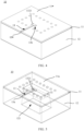
- a waveguide antenna assembly 10 may include an adapter structure 13 and a waveguide antenna (not shown in the figure), the adapter structure 13 is disposed on a first substrate 11, and the waveguide antenna is disposed on a second substrate 12.
- the first substrate 11 has a first board surface 11a (for example, an upper board surface in FIG. 4 ) and a second board surface (for example, a lower board surface in FIG. 4 ), and the second board surface is opposite to the first board surface 11a.
- the adapter structure 13 is configured to implement conversion between a microstrip signal and a waveguide signal.
- an electrical signal propagated in a microstrip is a TEM wave (transverse electromagnetic wave)
- an electrical signal propagated in a waveguide structure is a TE wave (transverse electric wave).
- the TEM wave is an electromagnetic wave whose electric and magnetic fields are on a plane perpendicular to a propagation direction of the electromagnetic wave.
- the TE wave is an electromagnetic wave whose electric field vector is perpendicular to a propagation direction of the electromagnetic wave.
- some magnetic field vectors of the TE wave are perpendicular to the propagation direction, and some magnetic field vectors are parallel to the propagation direction.
- the adapter structure 13 is configured to implement conversion between the TEM wave and the TE wave.
- the adapter structure 13 is approximately T-shaped, one end is a microstrip connection end 13a and may be connected to a microstrip, and the other end is a radiation end 1321 and may be configured to radiate an electromagnetic wave in a direction of the second substrate 12. Because the adapter structure 13 is disposed on the first substrate 11, the adapter structure 13 and the first substrate 11 may be considered as an overall structure, and a vertical projection of the radiation end 1321 on the second board surface 11b of the first substrate 11 may be considered as a waveguide connection end 13b.
- the waveguide connection end 13b is located on the second board surface, and may be coupled to the waveguide antenna (or a waveguide structure) disposed on the second board surface.
- the waveguide antenna is disposed on the second substrate 12, and the second substrate 12 may be manufactured by using a PCB process, that is, the waveguide antenna may be manufactured by using a process related to a process for producing a PCB. Because the PCB process is mature and stable, manufacturing costs and difficulty can be effectively reduced, and production quality can be ensured. This implements good matching between the adapter structure 13 and the waveguide antenna, and improves signal transmission efficiency and ensures performance of the waveguide antenna.
- the second substrate 12 is disposed on the second board surface 11b (the lower board surface in FIG. 4 ) of the first substrate 11, the second substrate 12 has a through hole 121 that penetrates the second substrate 12 in a thickness of the second substrate 12, and an inner wall of the through hole 121 has a conducting layer 122.
- the through hole 121 having the conducting layer 122 may transmit an electromagnetic wave to the outside or receive an electromagnetic wave from the outside, that is, the through hole 121 having the conducting layer 122 is configured to form the waveguide antenna, or the waveguide antenna may be understood as a combination of the through hole 121 and the conducting layer 122 located inside the through hole 121.
- a projection of the waveguide connection end 13b of the adapter structure 13 on the second substrate 12 is located in the through hole 121.
- An electromagnetic wave in the adapter structure 13 may be transmitted to the through hole 121 via the waveguide connection end 13b, and the electromagnetic wave is transmitted to the outside via the through hole 121.
- coupling represents effective transmission of an electromagnetic wave or energy between two components, but does not limit a mechanical structure connection relationship between the two components.
- a mechanical mechanism may be implemented by using a plurality of different types of manners.
- conversion between a microstrip structure and a waveguide structure may be implemented by using the adapter structure 13, to meet a signal transmission requirement between the microstrip and the waveguide antenna.
- the microstrip connection end 13a is located on the first board surface 11a
- the waveguide connection end 13b is located on the second board surface 11b, that is, the microstrip connection end 13a and the waveguide connection end 13b are located on different board surfaces of the first substrate 11. Therefore, different-plane signal transmission can be implemented.
- the adapter structure 13 is used to implement not only signal conversion between the microstrip and a waveguide, but also different-plane signal transmission.
- a component such as a radio frequency chip (not shown in the figure) on the first board surface 11a, thereby facilitating disposing of a heat dissipation structure configured to dissipate heat for the component such as the radio frequency chip.
- the through hole 121 having the conducting layer 122 disposed on the inner wall can implement a function of the waveguide antenna, manufacturing costs and a volume can be reduced.
- a conventional waveguide antenna is usually manufactured by using a metal machining or plastic electroplating process. Therefore, manufacturing efficiency is low, a manufacturing process is complex, and manufacturing precision is low.
- the second substrate 12 may use a PCB board as a raw material. Therefore, material costs can be effectively reduced.
- a volume of a conventional waveguide antenna is usually large (for example, a thickness is approximately 10 mm to 20 mm).
- the second substrate 12 may use a PCB material. Therefore, a thickness of the waveguide antenna can be effectively controlled (for example, less than 3 mm), and a volume of the waveguide antenna assembly 10 can be reduced.
- both the first substrate 11 and the second substrate 12 may use board structures, when the first substrate 11 and the second substrate 12 are assembled, assembly precision is improved, so that position precision between the adapter structure 13 and the through hole 121 can be ensured, a gap can be effectively avoided, and quality of signal transmission between the adapter structure 13 and the through hole 121 can be ensured.
- the microstrip adapter structure 13 may be directly coupled to the waveguide antenna through the waveguide connection end 13b, a signal transmission path can be effectively reduced, and an insertion loss of the waveguide antenna assembly 10 can be reduced.
- the waveguide antenna assembly 10 in this embodiment of this application may be used to reduce the insertion loss by about 0.5 dB.
- the first substrate 11 may use a printed circuit board (printed circuit board, PCB) or a flexible printed circuit (flexible printed circuit, FPC), or may be a board body structure of another type.
- the first substrate 11 may be a single-layer board, or may be a board disposed with two, three, or more layers in a stacked manner.
- a specific material of the first substrate 11 and a specific quantity of layers of the first substrate 11 are not limited in this application.
- the first board surface 11a and the second board surface 11b are two outer surfaces that are of the first substrate 11 and that are opposite to each other.
- the first board surface 11a and the second board surface 11b are respectively board surfaces that are of the first substrate 11 and that are opposite to each other.
- the first board surface 11a and the second board surface 11b are respectively outer board surfaces of two outermost boards of the first substrate 11.
- a fixed connection between the first substrate 11 and the second substrate 12 may be implemented via a connection layer (not shown in the figure).
- a material of the connection layer may be a material such as polypropylene (polypropylene, PP).
- a fixed connection between the first substrate 11 and the second substrate 12 may be alternatively implemented by using a connecting piece such as a screw.
- a connection manner between the first substrate 11 and the second substrate 12 is not specifically limited in this application.
- the through hole 121 may be first manufactured on the second substrate 12, and the adapter structure 13 may be manufactured on the first substrate 11. Then, the second substrate 12 is fastened to the second board surface of the first substrate 11, to implement a fixed connection between the first substrate 11 and the second substrate 12. In addition, coupling between the adapter structure 13 and the through hole 121 can also be implemented. Alternatively, the second substrate 12 may be first fastened to the second board surface of the first substrate 11, and then structures such as the through hole 121 and the conducting layer 122 are manufactured on the second substrate 12. This is not specifically limited in this application.
- the conducting layer 122 may use a metal material with good conductivity, such as copper or aluminum.
- a process such as electroplating or vapor deposition may be used for manufacturing.
- a specific material and a manufacturing process that are of the conducting layer 122 are not limited in this application.
- the through hole 121 may have various shapes.
- the through hole 121 is divided into two segments: a first segment 121a and a second segment 121b, the first segment 121a is disposed close to the first substrate 11, and the second segment 121b is disposed away from the first substrate 11.
- the first segment 121a is a straight through hole, that is, the first segment 121a has an approximately consistent aperture.
- the aperture may be effectively controlled. This helps perform high-precision coupling with the waveguide connection end 13b of the first substrate 11.
- cross-sectional areas of the second segment 121b gradually increase, that is, a diameter of the second segment 121b of the through hole 121 is proportional to a distance between the through hole 121 and the first substrate 11. This effectively takes a radiation range and a gain that are of the antenna into consideration, and helps improve operating performance of the antenna.
- cross-sectional areas of the through hole 121 gradually increase in the direction away from the first substrate 11 (a direction from top to bottom in the figure).
- the diameter of the through hole 121 may be proportional to the distance between the through hole 121 and the first substrate 11. This effectively takes the radiation range and the gain that are of the antenna into consideration, and helps improve operating performance of the waveguide antenna assembly 10.
- the inner wall of the through hole 121 is step-shaped in an axial direction of the through hole 121.
- the cross-sectional area of the through hole 121 increases in a stepwise manner.
- the through hole may be divided into a plurality of segments in the axial direction. In each segment, areas of cross sections of the through hole are approximately the same, and areas of cross sections between two adjacent segments are obviously different.
- drill bits with different diameters may be used to open each segment separately. This helps reduce manufacturing difficulty.
- a quantity of steps and a gradient may be properly adjusted based on an actual situation. This is not limited in this application.
- a disposing size of the through hole 121, a shape of the inner wall, and an increase amplitude of the disposing size may be properly set based on an actual situation, and a cross-sectional shape of the through hole 121 may be a circle, an ellipse, a polygon, or an irregular shape. This is not specifically limited in this application.
- the second substrate 12 is a single-layer board. It may be understood that, in another implementation, the second substrate 12 may be a plurality of boards disposed in a stacked manner. In actual application, the second substrate 12 may be a printed circuit board (printed circuit board, PCB) or a flexible printed circuit board (flexible printed circuit, FPC), or may be a board body structure of another type, or a specific material of the second substrate 12 and a quantity of layers of the second substrate 12 may be properly adjusted based on an actual requirement. This is not specifically limited in this application.
- PCB printed circuit board
- FPC flexible printed circuit
- the adapter structure 13 may use a plurality of different types of structures that can implement conversion between a microstrip and a waveguide.
- the adapter structure 13 may be a probe waveguide structure.
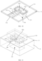
- the probe waveguide structure may include a floor 131, a transmission line 132, and a waveguide cavity 133. Both the floor 131 and the transmission line 132 are disposed on the first board surface (not shown in the figure) of the first substrate 11, the floor 131 is provided with a through groove 1311, and the transmission line 132 is disposed in the through groove 1311.
- the through groove 1311 and the transmission line 132 are an approximately T-shaped.
- One end of the transmission line 132 has the microstrip connection end 13a, and the other end is the radiation end 1321 and is configured to generate an electromagnetic wave.
- a transition part of a T-shaped structure of the transmission line 132 may be used to implement conversion and impedance conversion between a microstrip signal and a waveguide signal.
- the waveguide cavity 133 is disposed on the second board surface (not shown in the figure) of the first substrate 11, and an end that is of the waveguide cavity 133 and that is away from the first substrate 11 forms the waveguide connection end 13b.
- a signal is transmitted in a direction from the microstrip connection end 13a to the radiation end 1321, the signal is converted from a microstrip signal to a waveguide signal in the transition part of the T-shaped structure, and the waveguide signal is transmitted to the waveguide cavity 133 via the radiation end 1321.
- the end that is of the waveguide cavity 133 and that is away from the first substrate 11 may be coupled to the through hole (or a waveguide antenna), that is, the waveguide cavity 133 may play a function of bridging waveguide signals.
- the waveguide cavity 133 may be a dielectric waveguide, a metal waveguide, or the like.
- a specific structure type of the waveguide cavity 133 is not limited in this application.
- the waveguide cavity 133 may alternatively be omitted, and one end of the through hole 121 may directly abut against the second board surface and be coupled to the radiation end 1321. That is, a projection of the radiation end 1321 on the second board surface may form the waveguide connection end 13b.
- the transmission line 132 may alternatively include another structure that can implement impedance conversion, such as a microstrip gradient transition structure, to implement conversion between a microstrip signal and a waveguide signal, and specific shapes of the transmission line 132 and the through groove 1311 are not limited in this application.
- some electromagnetic waves generated at the radiation end 1321 may propagate in a direction away from the second substrate 12.
- the waveguide antenna assembly 10 is further provided with a back cavity 134.
- the back cavity 134 is disposed on the first board surface (not shown in the figure) of the first substrate 11, and is configured to reflect an electromagnetic wave generated at the radiation end 1321.
- the bottom wall of the back cavity 134 has a metal wall 1341.
- the metal wall 1341 reflects the electromagnetic wave, so that the electromagnetic wave can be transmitted in a direction toward the second substrate 12. This can effectively improve efficiency of transmitting the electromagnetic wave, and reduce a signal loss.
- the back cavity 134 may be manufactured by using an insulation material such as plastic, and the metal wall 1341 may be a conductive material, such as copper, that is manufactured on the bottom wall of the back cavity 134 by using a process such as electroplating or coating.
- the back cavity 134 may be manufactured by using a conductive material such as copper or aluminum, and the bottom wall of the back cavity 134 may form the metal wall 1341.
- Materials, that is, manufacturing processes, of the back cavity 134 and the bottom wall are not limited in this application.
- a distance between the metal wall 1341 and the radiation end 1321 may be a quarter of a wavelength at which the electromagnetic wave generated at the radiation end 1321 propagates in space, so that the metal wall 1341 can effectively reflect the electromagnetic wave. It may be understood that during specific implementation, the distance between the radiation end 1321 and the metal wall 1341 may be properly adjusted based on an actual requirement. This is not specifically limited in this application.
- a metallized hole 135 may be disposed on a side that is of the floor 131 and that faces the transmission line 132.
- parameters such as a quantity, positions, and sizes of metallized holes 135 may be properly set based on an actual requirement. This is not specifically limited in this application.
- the adapter structure 13 may be a substrate integrated waveguide (substrate integrated waveguide, SIW).
- SIW substrate integrated waveguide
- the substrate integrated waveguide is a structure in a form of a microwave transmission line, and implements a field propagation mode of a waveguide on a dielectric substrate by using the metallized hole 138.
- the substrate integrated waveguide mainly includes a dielectric substrate (not shown in the figure), an upper metal layer 136 is disposed on an upper board surface of the dielectric substrate, and a lower metal layer 137 is disposed on a lower board surface of the dielectric substrate.
- a plurality of metallized holes 138 are arranged in rows in the dielectric substrate, and penetrate from the upper metal layer 136 to the lower metal layer 137.
- the substrate integrated waveguide may be directly manufactured in the first substrate 11. That is, the first substrate 11 may be used as the dielectric substrate.
- a gap 1371 is disposed at the lower metal layer 137 of the substrate integrated waveguide, and an electric wall 139 is disposed at one end (a right end in the figure) of the substrate integrated waveguide. The electric wall 139 can effectively block the electromagnetic wave in the integrated waveguide, so that the electromagnetic wave can propagate outward through the gap 1371.
- the electric wall 139 includes a plurality of metallized holes disposed in rows. It may be understood that, in another implementation, the electric wall 139 may alternatively be a structure that can block an electromagnetic wave, such as a metal layer or a metal sheet. This is not specifically limited in this application.
- a distance between the electric wall 139 and the gap 1371 may be 0.25 times a wavelength at which an electromagnetic wave propagates in the substrate integrated waveguide (for example, the first substrate 11), so that the electromagnetic wave can efficiently propagate outward from the gap 1371.
- a size and a shape that are of the gap 1371 and the distance between the gap 1371 and the electric wall 139 may be properly adjusted based on an actual situation. This is not specifically limited in this application.
- the adapter structure 13 may alternatively use another type of structure that can implement conversion between a microstrip signal and a waveguide signal. This is not specifically limited in this application.
- the waveguide antenna assembly 10 includes one adapter structure 13 and one through hole 121
- two or more adapter structures 13 may be disposed in the first substrate 11, and two or more through holes 121 may be disposed in the second substrate 12.
- a quantity of disposed adapter structures 13 and a quantity of disposed through holes 121 may be the same, and the adapter structures 13 and the through holes 121 may be disposed in a one-to-one correspondence.
- the waveguide antenna assembly may include four adapter structures, the four adapter structures are all connected to a same radio frequency chip, and each adapter structure is coupled to a corresponding waveguide antenna. It may be understood that the foregoing is merely used as an example for reference, and in actual application, a quantity and positions of disposed waveguide antennas and disposed adapter structures may be properly selected and adjusted based on an actual requirement. This is not limited in this application.
- a data diagram that can represent an operating bandwidth of the waveguide antenna assembly 10 shown in FIG. 11 is provided.
- a horizontal coordinate indicates a frequency in GHz
- a vertical coordinate indicates an amplitude in dB.
- a frequency whose amplitude is less than -15 dB is usually used as an operating bandwidth of a waveguide antenna.
- a curve S1 represents a data diagram in which an amplitude varies with a frequency. It can be obviously seen from FIG. 17 that an operating frequency band of a waveguide antenna is approximately from 74.5 GHz to 89.5 GHz, that is, a bandwidth of the antenna is approximately 15 GHz. Therefore, the waveguide antenna has a good operating bandwidth.
- an antenna pattern that can represent a gain of the waveguide antenna assembly 10 shown in FIG. 11 is provided.
- a horizontal coordinate indicates an angle in degree, and a horizontal coordinate indicates a gain in dB.
- a curve S2 represents an H-plane antenna pattern obtained by measuring the waveguide antenna assembly 10 at an operating frequency of 79 GHz.
- a curve S3 represents an E-plane antenna pattern obtained by measuring the waveguide antenna assembly 10 at the operating frequency of 79 GHz.
- An H-plane may also be referred to as a magnetic plane, and is a plane parallel to a direction of a magnetic field.
- An E-plane may also be referred to as an electric plane, and is a plane parallel to a direction of an electric field. It can be obviously seen from FIG. 18 that the waveguide antenna assembly 10 can achieve a radiation gain of more than 7 dB.
- FIG. 19 is an antenna pattern of the waveguide antenna assembly 10 shown in FIG. 11 . It can be obviously seen from FIG. 19 that an antenna has a good radiation gain in a specific angle range (for example, from -120° to 120°), and a pattern shape is regular. Therefore, the antenna has good operating performance.
- a specific angle range for example, from -120° to 120°
- the waveguide antenna assembly 10 may further include a shielding can 15.
- the shielding can 15 may be disposed on a surface that is of the radio frequency chip 14 and that is away from the first substrate 11, to shield an electromagnetic wave.
- an electromagnetic wave may be generated in an operating process of a radio frequency signal, and the shielding can 15 may perform electromagnetic shielding on the electromagnetic wave, to prevent electromagnetic interference caused by the radio frequency chip 14 to another electronic component.
- the shielding can 15 may perform electromagnetic shielding on an electromagnetic wave generated by another electronic component, to ensure operating stability of the radio frequency chip 14.
- the shielding can 15 may be attached to the radio frequency chip 14, or it may be understood that the shielding can 15 may be in thermal contact with the radio frequency chip 14, so that heat generated by the radio frequency chip 14 can be transferred to the shielding can 15 through heat conduction. This can improve heat dissipation performance of the radio frequency chip 14.
- the shielding can 15 may be manufactured by using a conductive material like copper or aluminum, to effectively ensure electromagnetic shielding effect and provide good thermal conductivity. It may be understood that in specific application, a shape and a material that are of the shielding can 15 may be properly set based on an actual requirement. This is not specifically limited in this application.
- the shielding can 15 may further be in thermal contact with the back cavity 134, to improve heat dissipation effect of the radio frequency chip 14.
- the back cavity 134 and the shielding can 15 may be of an integrated structure. This is not specifically limited in this application.
- a metasurface 130 may be disposed at an end that is of the through hole 121 and that is away from the second substrate 12.
- the metasurface 130 is an artificial layered structure with a thickness less than a wavelength.
- the metasurface 130 can flexibly and effectively adjust characteristics such as polarization, an amplitude, a phase, a polarization mode, and a propagation mode of an electromagnetic wave. Therefore, in this embodiment provided in this application, the metasurface 130 can flexibly and effectively adjust the foregoing characteristics of an electromagnetic wave emitted through the through hole 121. This can improve operating performance of the waveguide antenna assembly 10.
- a thickness of the metasurface 130 is less than a wavelength means that a corresponding wavelength at which an electromagnetic wave in the through hole 121 propagates in space.
- the through hole 121 in the second substrate 12 can implement a function of a waveguide antenna, that is, the waveguide antenna may be manufactured by using a PCB process, the metasurface 130 can be efficiently and conveniently disposed on a lower surface of the second substrate 12. This can effectively improve convenience of manufacturing.
- the waveguide antenna assembly 10 may be used in a plurality of different types of electronic devices.
- the waveguide antenna assembly 10 may be used in a radar.
- the radar may include a housing and any one of the foregoing waveguide antenna assemblies 10, and the waveguide antenna assembly 10 may be disposed in the housing.
- the housing In terms of electrical performance, the housing has good electromagnetic wave penetration, so that normal receiving/sending of an electromagnetic wave between the waveguide antenna assembly 10 and the outside are not affected.
- the housing In terms of mechanical performance, the housing has good performance such as force bearing and antioxidation, so that the housing can withstand corrosion from an external harsh environment, and the housing can well protect the waveguide antenna assembly 10. It may be understood that, in specific application, a specific shape and a material that are of the housing may be properly set based on an actual situation. This is not limited in this application.
- the radar may be used in a terminal such as a vehicle or a drone, to implement a function such as wireless signal transmission or detection.
- the terminal is a vehicle.
- the vehicle may be equipped with the foregoing radar.
- the radar may be a long-range millimeter-wave radar, a medium-range/short-range millimeter-wave radar, or the like shown in the figure.
- different dotted lines indicate approximate detection ranges of different radars or cameras.
- a vehicle may be equipped with devices such as radars and cameras with a plurality of different detection types or detection ranges, to achieve a better detection function. This is not limited in this application.
- the waveguide antenna assembly 10 may be directly used in a radio frequency device or another device configured to perform communication by using an electromagnetic wave.
- a specific application scenario of the radar (or the waveguide antenna assembly 10) is not limited in this application.
- an embodiment of this application further provides a method for producing the waveguide antenna assembly 10.
- the method may include the following steps.
- Step S100 Provide a first substrate.
- the first substrate has a first board surface and a second board surface opposite to the first board surface.
- the first substrate has an adapter structure, the adapter structure is configured to implement conversion between a microstrip signal and a waveguide signal, the adapter structure has a microstrip connection end and a waveguide connection end, the microstrip connection end is located on the first board surface, and the waveguide connection end is located on the second board surface.
- S200 Provide a second substrate, dispose, on the second substrate, a through hole that penetrates the second substrate in a thickness direction of the second substrate, and dispose a conducting layer on an inner wall of the through hole.
- Step S300 Dispose the second substrate on the second board surface of the first substrate.
- the first substrate 11 and the second substrate 12 are separated from each other.
- the first substrate 11 may be a printed circuit board (printed circuit board, PCB) or a flexible printed circuit (flexible printed circuit, FPC) that has an adapter structure, and the first substrate 11 may be a single-layer board or a multi-layer board.
- the adapter structure may include a probe waveguide structure, may include a substrate integrated waveguide structure, or may include another structure that can implement conversion between a microstrip signal and a waveguide signal. This is not specifically limited in this application.
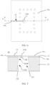
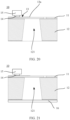
- the substrate integrated waveguide includes an upper metal layer 136 located on the first board surface (an upper board surface in FIG. 24 ) of the first substrate 11 and a lower metal layer 137 located on the second board surface (a lower board surface in FIG. 24 ) of the first substrate 11, and an electromagnetic wave may propagate (for example, propagate from left to right) between the upper metal layer 136 and the lower metal layer 137.
- a gap 1371 is disposed at the lower metal layer 137, so that the electromagnetic wave can propagate to the through hole 121 through the gap 1371.
- a process such as etching or machining may be used for production.
- a process of disposing the gap 1371 may be properly selected based on an actual situation. This is not specifically limited in this application.
- the second substrate 12 may be a printed circuit board (printed circuit board, PCB) or a flexible printed circuit (flexible printed circuit, FPC), and the second substrate 12 may be a single-layer board or a multi-layer board.
- PCB printed circuit board
- FPC flexible printed circuit
- An upper board surface of the second substrate 12 has an upper metal layer 12a, and a lower board surface of the second substrate 12 is provided with a lower metal layer 12b.
- the second substrate 12 is provided with the through hole 121, an upper end of the through hole 121 penetrates the upper metal layer 12a, and a lower end of the through hole 121 penetrates the lower metal layer 12b.
- apertures of the through hole 121 gradually increase in a direction away from the first substrate 11.
- the through hole 121 may be disposed by using a process such as etching or machining. Certainly, in actual application, a process for disposing the through hole 121 may be properly selected based on an actual situation. This is not specifically limited in this application.
- the through hole 121 may be a stepped hole or in a structure of another shape. A specific shape of the through hole 121 is not limited in this application.
- the conducting layer 122 may be disposed on the inner wall of the through hole 121, so that the through hole 121 can have a function of a waveguide antenna.
- the conducting layer 122 may be manufactured by using a process such as electroplating.
- a material of the conducting layer 122 may be copper, aluminum, or the like. A production process and the material that are of the conducting layer 122 are not limited in this application.
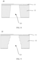
- the first substrate 11 and the second substrate 12 may be press-fitted by using a process such as thermal pressing, to implement a fixed connection between the first substrate 11 and the second substrate 12.
- a connection layer 100 may be disposed between the first substrate 11 and the second substrate 12.
- the connection layer 100 may be made of a material such as polypropylene (polypropylene, PP), to implement the fixed connection between the first substrate 11 and the second substrate 12.
- a blind hole 111 may be disposed on the first substrate 11.
- the bottom of the blind hole 111 penetrates the upper metal layer 12a of the second substrate 12. It may be understood that, in another implementation, the bottom of the blind hole 111 may alternatively penetrate the lower board surface of the first substrate 11. That is, the blind hole 111 may not penetrate the connection layer 100 or the lower metal layer 137.
- the first substrate 11 and the second substrate 12 may use a board with a large area. Therefore, a separation hole 112 that penetrates the first substrate 11 and the second substrate 12 may be disposed, to obtain, through separation, a waveguide antenna assembly of a required shape and size.
- a metal layer 1111 may be subsequently disposed in the blind hole 111 to form an electric wall, and a metal layer 1121 may be disposed in the separation hole 112.
- a main function of the electric wall is to block an electromagnetic wave in the first substrate 11, so that the electromagnetic wave can propagate to the through hole 121 through the gap 1371.
- a plurality of blind holes 111 may be disposed, and the blind holes 111 are disposed in rows.
- the blind hole 111 may alternatively be replaced with a long groove or another structure.
- the electric wall may be a metal sheet or the like. A specific structure of the electric wall is not limited in this application.
- a notch 113 may be disposed on the lower surface of the second substrate 12 by using a process such as etching, to produce a waveguide antenna of a required shape and size.
- a metasurface (not shown in the figure) may alternatively be disposed on a lower side (a side away from the first substrate 11) of the through hole 121, to improve operating performance of the waveguide antenna assembly.
- a specific type and a disposing manner that are of the metasurface are not limited in this application.
- the gap 1371 may be first disposed in the first substrate 11, the through hole 121 may be disposed in the second substrate 12, and then the first substrate 11 and the second substrate 12 are press-fitted.
- a production sequence may be further flexibly adjusted.
- an embodiment of this application further provides another production method.
- the method includes step S110: Provide a first substrate.
- the first substrate has a first board surface and a second board surface opposite to the first board surface.
- the first substrate has an adapter structure, the adapter structure is configured to implement conversion between a microstrip signal and a waveguide signal, the adapter structure has a microstrip connection end and a waveguide connection end, the microstrip connection end is located on the first board surface, and the waveguide connection end is located on the second board surface.
- Step S210 Provide a second substrate, and dispose the second substrate on the second board surface of the first substrate.
- S310 Dispose, on the second substrate, a through hole that penetrates the second substrate in a thickness direction of the second substrate, and dispose a conducting layer on an inner wall of the through hole.
- the second substrate 12 may be disposed on a lower board surface of the first substrate 11 via a connection layer 100.
- Specific structures and materials of the first substrate 11, the second substrate 12, and the connection layer 100 may be disposed similar to types in the foregoing examples. Details are not described herein again.
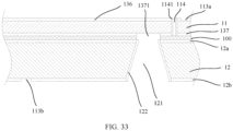
- a blind hole 114 may be disposed on the first substrate 11 by using a process such as machining, and the through hole 121 may be disposed on the second substrate 12.
- the bottom of the blind hole 114 may penetrate the connection layer 100, and an upper end of the through hole 121 may penetrate a lower metal layer 137 of the first substrate 11.
- the conducting layer 1141 may be disposed on an inner wall of the blind hole 114, and the conducting layer 122 may be disposed on the inner wall of the through hole 121.
- the blind hole 114 having the conducting layer 1141 may form an electric wall, and the through hole 121 having the conducting layer 122 may form a waveguide antenna.
- a process such as etching may be used to open a gap 1371 at a position that corresponds to the through hole 121 that is on a lower board surface of the second substrate, so that an electromagnetic wave can propagate to the through hole 121 through the gap 1371.
- structures such as notches 113a and 113b may be respectively disposed on an upper metal layer 136 of an upper board surface of the first substrate 11 and a lower metal layer 12b of the lower board surface of the second substrate 12, to produce a waveguide antenna assembly with a required shape profile.
- structures such as the gap 1371 may be first disposed in the first substrate 11, structures such as the through hole 121 (waveguide antenna) may be disposed in the second substrate 12, and then the first substrate 11 and the second substrate 12 are press-fitted.
- the first substrate 11 and the second substrate 12 may be first press-fitted, then structures such as the through hole 121 (or a waveguide antenna) are disposed in the second substrate 12, and structures such as the gap 1371 are disposed in the first substrate 11, to produce the waveguide antenna assembly.
Landscapes
- Engineering & Computer Science (AREA)
- Remote Sensing (AREA)
- Physics & Mathematics (AREA)
- Computer Security & Cryptography (AREA)
- Radar, Positioning & Navigation (AREA)
- Aviation & Aerospace Engineering (AREA)
- Electromagnetism (AREA)
- Astronomy & Astrophysics (AREA)
- General Physics & Mathematics (AREA)
- Waveguide Aerials (AREA)
- Variable-Direction Aerials And Aerial Arrays (AREA)
Applications Claiming Priority (2)
| Application Number | Priority Date | Filing Date | Title |
|---|---|---|---|
| CN202210346782.9A CN114784489B (zh) | 2022-03-31 | 2022-03-31 | 波导天线组件、雷达、终端和波导天线组件的制备方法 |
| PCT/CN2023/084390 WO2023185843A1 (zh) | 2022-03-31 | 2023-03-28 | 波导天线组件、雷达、终端和波导天线组件的制备方法 |
Publications (2)
| Publication Number | Publication Date |
|---|---|
| EP4498518A1 true EP4498518A1 (de) | 2025-01-29 |
| EP4498518A4 EP4498518A4 (de) | 2025-06-25 |
Family
ID=82427246
Family Applications (1)
| Application Number | Title | Priority Date | Filing Date |
|---|---|---|---|
| EP23778208.1A Pending EP4498518A4 (de) | 2022-03-31 | 2023-03-28 | Wellenleiterantennenanordnung, radar, endgerät und herstellungsverfahren für wellenleiterantennenanordnung |
Country Status (3)
| Country | Link |
|---|---|
| EP (1) | EP4498518A4 (de) |
| CN (1) | CN114784489B (de) |
| WO (1) | WO2023185843A1 (de) |
Families Citing this family (9)
| Publication number | Priority date | Publication date | Assignee | Title |
|---|---|---|---|---|
| FR3099132B1 (fr) * | 2019-07-26 | 2022-01-28 | Mbda France | Capot pour vehicule, en particulier pour vehicule supersonique ou hypersonique |
| CN114784489B (zh) * | 2022-03-31 | 2024-01-16 | 华为技术有限公司 | 波导天线组件、雷达、终端和波导天线组件的制备方法 |
| CN117154408A (zh) * | 2022-10-26 | 2023-12-01 | 深圳Tcl数字技术有限公司 | 毫米波天线组件以及显示装置 |
| CN115494456B (zh) * | 2022-11-21 | 2023-03-10 | 南京隼眼电子科技有限公司 | 雷达收发装置及雷达装置 |
| CN116190960B (zh) * | 2023-03-29 | 2025-05-13 | 东南大学 | 一种太赫兹频段低损耗高集成度的芯片波导转接结构 |
| CN116683167B (zh) * | 2023-06-16 | 2024-07-30 | 深圳承泰科技有限公司 | 一种塑料电镀波导天线及其制作方法 |
| CN118174008A (zh) * | 2024-03-29 | 2024-06-11 | 环旭电子股份有限公司 | 天线结构与天线模块 |
| CN119209010B (zh) * | 2024-10-16 | 2025-10-03 | 中国科学院微电子研究所 | 一种太赫兹喇叭天线及其制备方法 |
| CN119852695B (zh) * | 2025-03-24 | 2025-07-18 | 北京理工大学 | 基于ltcc工艺的高频毫米波三维立体集成天线阵列 |
Family Cites Families (15)
| Publication number | Priority date | Publication date | Assignee | Title |
|---|---|---|---|---|
| TW293957B (en) * | 1996-08-05 | 1996-12-21 | Chyng-Guang Juang | The structure and the feeding method of the microstrip leaky-wave antenna |
| JP2006191428A (ja) * | 2005-01-07 | 2006-07-20 | Japan Radio Co Ltd | マイクロストリップ線路導波管変換器 |
| JP2008193243A (ja) * | 2007-02-01 | 2008-08-21 | Hitachi Kokusai Electric Inc | 導波管 |
| CN101436702A (zh) * | 2008-12-12 | 2009-05-20 | 惠州市硕贝德通讯科技有限公司 | 一种波导—微带线变换及功率分配器 |
| EP2267832A1 (de) * | 2009-06-11 | 2010-12-29 | Imec | Integriertes System mit einem Wellenleiter für eine Mikrostreifen-Kopplungsvorrichtung |
| US9577340B2 (en) * | 2014-03-18 | 2017-02-21 | Peraso Technologies Inc. | Waveguide adapter plate to facilitate accurate alignment of sectioned waveguide channel in microwave antenna assembly |
| DE112015005575T5 (de) * | 2014-12-12 | 2017-09-28 | Sony Corporation | Mikrowellenantennenvorrichtung, einheit und herstellungsverfahren |
| US9865935B2 (en) * | 2015-01-12 | 2018-01-09 | Huawei Technologies Co., Ltd. | Printed circuit board for antenna system |
| DE112017001710T5 (de) * | 2016-04-01 | 2018-12-20 | Sony Corporation | Mikrowellenantenneneinrichtung, Verpackungs- und Herstellungsverfahren |
| WO2018116416A1 (ja) * | 2016-12-21 | 2018-06-28 | 三菱電機株式会社 | 導波管マイクロストリップ線路変換器およびアンテナ装置 |
| CN107394395B (zh) * | 2017-07-07 | 2020-10-27 | 东南大学 | 基于平面正交模耦合器的双极化喇叭天线 |
| KR102572820B1 (ko) * | 2018-11-19 | 2023-08-30 | 삼성전자 주식회사 | 혼 구조를 이용한 안테나 및 그것을 포함하는 전자 장치 |
| CN112467326B (zh) * | 2020-12-07 | 2021-10-01 | 之江实验室 | 一种宽带矩形波导-微带转换器 |
| CN112563708B (zh) * | 2021-02-22 | 2021-06-04 | 成都天锐星通科技有限公司 | 一种传输线转换结构与天线驻波测试系统 |
| CN114784489B (zh) * | 2022-03-31 | 2024-01-16 | 华为技术有限公司 | 波导天线组件、雷达、终端和波导天线组件的制备方法 |
-
2022
- 2022-03-31 CN CN202210346782.9A patent/CN114784489B/zh active Active
-
2023
- 2023-03-28 WO PCT/CN2023/084390 patent/WO2023185843A1/zh not_active Ceased
- 2023-03-28 EP EP23778208.1A patent/EP4498518A4/de active Pending
Also Published As
| Publication number | Publication date |
|---|---|
| CN114784489B (zh) | 2024-01-16 |
| WO2023185843A1 (zh) | 2023-10-05 |
| WO2023185843A9 (zh) | 2023-11-09 |
| EP4498518A4 (de) | 2025-06-25 |
| CN114784489A (zh) | 2022-07-22 |
Similar Documents
| Publication | Publication Date | Title |
|---|---|---|
| CN114784489B (zh) | 波导天线组件、雷达、终端和波导天线组件的制备方法 | |
| CN111066201B (zh) | 相控阵天线 | |
| EP3301758A1 (de) | Antennenelement | |
| JP3996879B2 (ja) | 誘電体導波管とマイクロストリップ線路の結合構造およびこの結合構造を具備するフィルタ基板 | |
| US12482745B2 (en) | Wireless interconnect for high-rate data transfer | |
| CN115764256A (zh) | 毫米波雷达天线和车辆 | |
| CN111771304A (zh) | 一种假天线结构以及毫米波天线阵列 | |
| CN117954843B (zh) | 一种毫米波雷达射频前端模组 | |
| EP3893329A1 (de) | Antenne zum senden und/oder empfangen von elektromagnetischen signalen | |
| US12237590B2 (en) | Printed circuit board integrated antenna for transmitting / receiving data | |
| CN218827835U (zh) | 共面馈电波导缝隙天线及雷达 | |
| CN117913517A (zh) | 一种基于微波多层板的脊波导相控阵天线 | |
| CN116937182A (zh) | 一种模块化毫米波阵列天线 | |
| CN116014400A (zh) | 一种矩形波导、喇叭天线及片上系统 | |
| JP4713367B2 (ja) | 開口面アンテナ | |
| CN210167505U (zh) | 一种宽带siw缝隙天线 | |
| JP4799238B2 (ja) | 開口面アンテナ | |
| RU2780558C1 (ru) | Встраиваемая в печатную плату антенна передачи/приема данных | |
| JP4439423B2 (ja) | アンテナ | |
| CN121748793A (zh) | 天线阵列及天线 | |
| CN120089943A (zh) | 多层混压印制板、毫米波收发天线阵列和人体安检系统 | |
| CN119093005B (zh) | 一种x频段高集成度低剖面宽角扫描微带天线阵列 | |
| CN115642397A (zh) | 一种馈电位置可变的两维相控阵天线单元 | |
| KR20260027935A (ko) | 안테나 소자, 안테나 어레이 및 안테나 모듈 | |
| CN121149668A (zh) | 一种基于pcb板的超宽带毫米波天线 |
Legal Events
| Date | Code | Title | Description |
|---|---|---|---|
| STAA | Information on the status of an ep patent application or granted ep patent |
Free format text: STATUS: THE INTERNATIONAL PUBLICATION HAS BEEN MADE |
|
| PUAI | Public reference made under article 153(3) epc to a published international application that has entered the european phase |
Free format text: ORIGINAL CODE: 0009012 |
|
| STAA | Information on the status of an ep patent application or granted ep patent |
Free format text: STATUS: REQUEST FOR EXAMINATION WAS MADE |
|
| 17P | Request for examination filed |
Effective date: 20241021 |
|
| AK | Designated contracting states |
Kind code of ref document: A1 Designated state(s): AL AT BE BG CH CY CZ DE DK EE ES FI FR GB GR HR HU IE IS IT LI LT LU LV MC ME MK MT NL NO PL PT RO RS SE SI SK SM TR |
|
| A4 | Supplementary search report drawn up and despatched |
Effective date: 20250523 |
|
| RIC1 | Information provided on ipc code assigned before grant |
Ipc: H01Q 3/30 20060101ALN20250519BHEP Ipc: H01P 5/107 20060101ALI20250519BHEP Ipc: H01Q 13/02 20060101ALI20250519BHEP Ipc: H01Q 1/52 20060101ALI20250519BHEP Ipc: H01Q 1/32 20060101ALI20250519BHEP Ipc: H01Q 1/36 20060101AFI20250519BHEP |
|
| DAV | Request for validation of the european patent (deleted) | ||
| DAX | Request for extension of the european patent (deleted) |