EP4498435A2 - Gate-all-around-feldeffekttransistor mit seitlich diffundiertem metalloxidhalbleiter - Google Patents
Gate-all-around-feldeffekttransistor mit seitlich diffundiertem metalloxidhalbleiter Download PDFInfo
- Publication number
- EP4498435A2 EP4498435A2 EP24190973.8A EP24190973A EP4498435A2 EP 4498435 A2 EP4498435 A2 EP 4498435A2 EP 24190973 A EP24190973 A EP 24190973A EP 4498435 A2 EP4498435 A2 EP 4498435A2
- Authority
- EP
- European Patent Office
- Prior art keywords
- sheets
- gate
- epitaxial layer
- disposed
- substrate
- Prior art date
- Legal status (The legal status is an assumption and is not a legal conclusion. Google has not performed a legal analysis and makes no representation as to the accuracy of the status listed.)
- Pending
Links
Images

Classifications
-
- H—ELECTRICITY
- H10—SEMICONDUCTOR DEVICES; ELECTRIC SOLID-STATE DEVICES NOT OTHERWISE PROVIDED FOR
- H10D—INORGANIC ELECTRIC SEMICONDUCTOR DEVICES
- H10D30/00—Field-effect transistors [FET]
- H10D30/40—FETs having zero-dimensional [0D], one-dimensional [1D] or two-dimensional [2D] charge carrier gas channels
- H10D30/43—FETs having zero-dimensional [0D], one-dimensional [1D] or two-dimensional [2D] charge carrier gas channels having one-dimensional [1D] charge carrier gas channels, e.g. quantum wire FETs or transistors having 1D quantum-confined channels
-
- B—PERFORMING OPERATIONS; TRANSPORTING
- B82—NANOTECHNOLOGY
- B82Y—SPECIFIC USES OR APPLICATIONS OF NANOSTRUCTURES; MEASUREMENT OR ANALYSIS OF NANOSTRUCTURES; MANUFACTURE OR TREATMENT OF NANOSTRUCTURES
- B82Y10/00—Nanotechnology for information processing, storage or transmission, e.g. quantum computing or single electron logic
-
- H—ELECTRICITY
- H10—SEMICONDUCTOR DEVICES; ELECTRIC SOLID-STATE DEVICES NOT OTHERWISE PROVIDED FOR
- H10D—INORGANIC ELECTRIC SEMICONDUCTOR DEVICES
- H10D30/00—Field-effect transistors [FET]
- H10D30/60—Insulated-gate field-effect transistors [IGFET]
- H10D30/601—Insulated-gate field-effect transistors [IGFET] having lightly-doped drain or source extensions, e.g. LDD IGFETs or DDD IGFETs
- H10D30/603—Insulated-gate field-effect transistors [IGFET] having lightly-doped drain or source extensions, e.g. LDD IGFETs or DDD IGFETs having asymmetry in the channel direction, e.g. lateral high-voltage MISFETs having drain offset region or extended drain IGFETs [EDMOS]
-
- H—ELECTRICITY
- H10—SEMICONDUCTOR DEVICES; ELECTRIC SOLID-STATE DEVICES NOT OTHERWISE PROVIDED FOR
- H10D—INORGANIC ELECTRIC SEMICONDUCTOR DEVICES
- H10D30/00—Field-effect transistors [FET]
- H10D30/60—Insulated-gate field-effect transistors [IGFET]
- H10D30/67—Thin-film transistors [TFT]
- H10D30/6729—Thin-film transistors [TFT] characterised by the electrodes
- H10D30/673—Thin-film transistors [TFT] characterised by the electrodes characterised by the shapes, relative sizes or dispositions of the gate electrodes
- H10D30/6735—Thin-film transistors [TFT] characterised by the electrodes characterised by the shapes, relative sizes or dispositions of the gate electrodes having gates fully surrounding the channels, e.g. gate-all-around
-
- H—ELECTRICITY
- H10—SEMICONDUCTOR DEVICES; ELECTRIC SOLID-STATE DEVICES NOT OTHERWISE PROVIDED FOR
- H10D—INORGANIC ELECTRIC SEMICONDUCTOR DEVICES
- H10D30/00—Field-effect transistors [FET]
- H10D30/60—Insulated-gate field-effect transistors [IGFET]
- H10D30/67—Thin-film transistors [TFT]
- H10D30/6757—Thin-film transistors [TFT] characterised by the structure of the channel, e.g. transverse or longitudinal shape or doping profile
-
- H—ELECTRICITY
- H10—SEMICONDUCTOR DEVICES; ELECTRIC SOLID-STATE DEVICES NOT OTHERWISE PROVIDED FOR
- H10D—INORGANIC ELECTRIC SEMICONDUCTOR DEVICES
- H10D62/00—Semiconductor bodies, or regions thereof, of devices having potential barriers
- H10D62/10—Shapes, relative sizes or dispositions of the regions of the semiconductor bodies; Shapes of the semiconductor bodies
- H10D62/113—Isolations within a component, i.e. internal isolations
- H10D62/114—PN junction isolations
-
- H—ELECTRICITY
- H10—SEMICONDUCTOR DEVICES; ELECTRIC SOLID-STATE DEVICES NOT OTHERWISE PROVIDED FOR
- H10D—INORGANIC ELECTRIC SEMICONDUCTOR DEVICES
- H10D62/00—Semiconductor bodies, or regions thereof, of devices having potential barriers
- H10D62/10—Shapes, relative sizes or dispositions of the regions of the semiconductor bodies; Shapes of the semiconductor bodies
- H10D62/117—Shapes of semiconductor bodies
- H10D62/118—Nanostructure semiconductor bodies
- H10D62/119—Nanowire, nanosheet or nanotube semiconductor bodies
- H10D62/121—Nanowire, nanosheet or nanotube semiconductor bodies oriented parallel to substrates
-
- H—ELECTRICITY
- H10—SEMICONDUCTOR DEVICES; ELECTRIC SOLID-STATE DEVICES NOT OTHERWISE PROVIDED FOR
- H10D—INORGANIC ELECTRIC SEMICONDUCTOR DEVICES
- H10D62/00—Semiconductor bodies, or regions thereof, of devices having potential barriers
- H10D62/10—Shapes, relative sizes or dispositions of the regions of the semiconductor bodies; Shapes of the semiconductor bodies
- H10D62/13—Semiconductor regions connected to electrodes carrying current to be rectified, amplified or switched, e.g. source or drain regions
- H10D62/149—Source or drain regions of field-effect devices
- H10D62/151—Source or drain regions of field-effect devices of IGFETs
-
- H—ELECTRICITY
- H10—SEMICONDUCTOR DEVICES; ELECTRIC SOLID-STATE DEVICES NOT OTHERWISE PROVIDED FOR
- H10D—INORGANIC ELECTRIC SEMICONDUCTOR DEVICES
- H10D62/00—Semiconductor bodies, or regions thereof, of devices having potential barriers
- H10D62/10—Shapes, relative sizes or dispositions of the regions of the semiconductor bodies; Shapes of the semiconductor bodies
- H10D62/13—Semiconductor regions connected to electrodes carrying current to be rectified, amplified or switched, e.g. source or drain regions
- H10D62/149—Source or drain regions of field-effect devices
- H10D62/151—Source or drain regions of field-effect devices of IGFETs
- H10D62/156—Drain regions of DMOS transistors
- H10D62/159—Shapes
-
- H—ELECTRICITY
- H10—SEMICONDUCTOR DEVICES; ELECTRIC SOLID-STATE DEVICES NOT OTHERWISE PROVIDED FOR
- H10D—INORGANIC ELECTRIC SEMICONDUCTOR DEVICES
- H10D62/00—Semiconductor bodies, or regions thereof, of devices having potential barriers
- H10D62/10—Shapes, relative sizes or dispositions of the regions of the semiconductor bodies; Shapes of the semiconductor bodies
- H10D62/17—Semiconductor regions connected to electrodes not carrying current to be rectified, amplified or switched, e.g. channel regions
- H10D62/351—Substrate regions of field-effect devices
- H10D62/357—Substrate regions of field-effect devices of FETs
- H10D62/364—Substrate regions of field-effect devices of FETs of IGFETs
- H10D62/371—Inactive supplementary semiconductor regions, e.g. for preventing punch-through, improving capacity effect or leakage current
-
- H—ELECTRICITY
- H10—SEMICONDUCTOR DEVICES; ELECTRIC SOLID-STATE DEVICES NOT OTHERWISE PROVIDED FOR
- H10D—INORGANIC ELECTRIC SEMICONDUCTOR DEVICES
- H10D64/00—Electrodes of devices having potential barriers
- H10D64/111—Field plates
-
- H—ELECTRICITY
- H10—SEMICONDUCTOR DEVICES; ELECTRIC SOLID-STATE DEVICES NOT OTHERWISE PROVIDED FOR
- H10D—INORGANIC ELECTRIC SEMICONDUCTOR DEVICES
- H10D84/00—Integrated devices formed in or on semiconductor substrates that comprise only semiconducting layers, e.g. on Si wafers or on GaAs-on-Si wafers
- H10D84/01—Manufacture or treatment
- H10D84/0123—Integrating together multiple components covered by H10D12/00 or H10D30/00, e.g. integrating multiple IGBTs
- H10D84/0126—Integrating together multiple components covered by H10D12/00 or H10D30/00, e.g. integrating multiple IGBTs the components including insulated gates, e.g. IGFETs
- H10D84/0128—Manufacturing their channels
-
- H—ELECTRICITY
- H10—SEMICONDUCTOR DEVICES; ELECTRIC SOLID-STATE DEVICES NOT OTHERWISE PROVIDED FOR
- H10D—INORGANIC ELECTRIC SEMICONDUCTOR DEVICES
- H10D84/00—Integrated devices formed in or on semiconductor substrates that comprise only semiconducting layers, e.g. on Si wafers or on GaAs-on-Si wafers
- H10D84/01—Manufacture or treatment
- H10D84/0123—Integrating together multiple components covered by H10D12/00 or H10D30/00, e.g. integrating multiple IGBTs
- H10D84/0126—Integrating together multiple components covered by H10D12/00 or H10D30/00, e.g. integrating multiple IGBTs the components including insulated gates, e.g. IGFETs
- H10D84/013—Manufacturing their source or drain regions, e.g. silicided source or drain regions
-
- H—ELECTRICITY
- H10—SEMICONDUCTOR DEVICES; ELECTRIC SOLID-STATE DEVICES NOT OTHERWISE PROVIDED FOR
- H10D—INORGANIC ELECTRIC SEMICONDUCTOR DEVICES
- H10D84/00—Integrated devices formed in or on semiconductor substrates that comprise only semiconducting layers, e.g. on Si wafers or on GaAs-on-Si wafers
- H10D84/80—Integrated devices formed in or on semiconductor substrates that comprise only semiconducting layers, e.g. on Si wafers or on GaAs-on-Si wafers characterised by the integration of at least one component covered by groups H10D12/00 or H10D30/00, e.g. integration of IGFETs
- H10D84/82—Integrated devices formed in or on semiconductor substrates that comprise only semiconducting layers, e.g. on Si wafers or on GaAs-on-Si wafers characterised by the integration of at least one component covered by groups H10D12/00 or H10D30/00, e.g. integration of IGFETs of only field-effect components
- H10D84/83—Integrated devices formed in or on semiconductor substrates that comprise only semiconducting layers, e.g. on Si wafers or on GaAs-on-Si wafers characterised by the integration of at least one component covered by groups H10D12/00 or H10D30/00, e.g. integration of IGFETs of only field-effect components of only insulated-gate FETs [IGFET]
- H10D84/8311—Integrated devices formed in or on semiconductor substrates that comprise only semiconducting layers, e.g. on Si wafers or on GaAs-on-Si wafers characterised by the integration of at least one component covered by groups H10D12/00 or H10D30/00, e.g. integration of IGFETs of only field-effect components of only insulated-gate FETs [IGFET] the IGFETs characterised by having different channel structures
-
- H—ELECTRICITY
- H10—SEMICONDUCTOR DEVICES; ELECTRIC SOLID-STATE DEVICES NOT OTHERWISE PROVIDED FOR
- H10D—INORGANIC ELECTRIC SEMICONDUCTOR DEVICES
- H10D84/00—Integrated devices formed in or on semiconductor substrates that comprise only semiconducting layers, e.g. on Si wafers or on GaAs-on-Si wafers
- H10D84/80—Integrated devices formed in or on semiconductor substrates that comprise only semiconducting layers, e.g. on Si wafers or on GaAs-on-Si wafers characterised by the integration of at least one component covered by groups H10D12/00 or H10D30/00, e.g. integration of IGFETs
- H10D84/82—Integrated devices formed in or on semiconductor substrates that comprise only semiconducting layers, e.g. on Si wafers or on GaAs-on-Si wafers characterised by the integration of at least one component covered by groups H10D12/00 or H10D30/00, e.g. integration of IGFETs of only field-effect components
- H10D84/83—Integrated devices formed in or on semiconductor substrates that comprise only semiconducting layers, e.g. on Si wafers or on GaAs-on-Si wafers characterised by the integration of at least one component covered by groups H10D12/00 or H10D30/00, e.g. integration of IGFETs of only field-effect components of only insulated-gate FETs [IGFET]
- H10D84/8312—Integrated devices formed in or on semiconductor substrates that comprise only semiconducting layers, e.g. on Si wafers or on GaAs-on-Si wafers characterised by the integration of at least one component covered by groups H10D12/00 or H10D30/00, e.g. integration of IGFETs of only field-effect components of only insulated-gate FETs [IGFET] the IGFETs characterised by having different source or drain region structures, e.g. IGFETs having symmetrical source or drain regions integrated with IGFETs having asymmetrical source or drain regions
-
- H—ELECTRICITY
- H10—SEMICONDUCTOR DEVICES; ELECTRIC SOLID-STATE DEVICES NOT OTHERWISE PROVIDED FOR
- H10D—INORGANIC ELECTRIC SEMICONDUCTOR DEVICES
- H10D84/00—Integrated devices formed in or on semiconductor substrates that comprise only semiconducting layers, e.g. on Si wafers or on GaAs-on-Si wafers
- H10D84/80—Integrated devices formed in or on semiconductor substrates that comprise only semiconducting layers, e.g. on Si wafers or on GaAs-on-Si wafers characterised by the integration of at least one component covered by groups H10D12/00 or H10D30/00, e.g. integration of IGFETs
- H10D84/82—Integrated devices formed in or on semiconductor substrates that comprise only semiconducting layers, e.g. on Si wafers or on GaAs-on-Si wafers characterised by the integration of at least one component covered by groups H10D12/00 or H10D30/00, e.g. integration of IGFETs of only field-effect components
- H10D84/83—Integrated devices formed in or on semiconductor substrates that comprise only semiconducting layers, e.g. on Si wafers or on GaAs-on-Si wafers characterised by the integration of at least one component covered by groups H10D12/00 or H10D30/00, e.g. integration of IGFETs of only field-effect components of only insulated-gate FETs [IGFET]
- H10D84/832—Integrated devices formed in or on semiconductor substrates that comprise only semiconducting layers, e.g. on Si wafers or on GaAs-on-Si wafers characterised by the integration of at least one component covered by groups H10D12/00 or H10D30/00, e.g. integration of IGFETs of only field-effect components of only insulated-gate FETs [IGFET] comprising IGFETs having stacked nanowire, nanosheet or nanoribbon channels
-
- H—ELECTRICITY
- H10—SEMICONDUCTOR DEVICES; ELECTRIC SOLID-STATE DEVICES NOT OTHERWISE PROVIDED FOR
- H10D—INORGANIC ELECTRIC SEMICONDUCTOR DEVICES
- H10D84/00—Integrated devices formed in or on semiconductor substrates that comprise only semiconducting layers, e.g. on Si wafers or on GaAs-on-Si wafers
- H10D84/80—Integrated devices formed in or on semiconductor substrates that comprise only semiconducting layers, e.g. on Si wafers or on GaAs-on-Si wafers characterised by the integration of at least one component covered by groups H10D12/00 or H10D30/00, e.g. integration of IGFETs
- H10D84/82—Integrated devices formed in or on semiconductor substrates that comprise only semiconducting layers, e.g. on Si wafers or on GaAs-on-Si wafers characterised by the integration of at least one component covered by groups H10D12/00 or H10D30/00, e.g. integration of IGFETs of only field-effect components
- H10D84/83—Integrated devices formed in or on semiconductor substrates that comprise only semiconducting layers, e.g. on Si wafers or on GaAs-on-Si wafers characterised by the integration of at least one component covered by groups H10D12/00 or H10D30/00, e.g. integration of IGFETs of only field-effect components of only insulated-gate FETs [IGFET]
- H10D84/836—Integrated devices formed in or on semiconductor substrates that comprise only semiconducting layers, e.g. on Si wafers or on GaAs-on-Si wafers characterised by the integration of at least one component covered by groups H10D12/00 or H10D30/00, e.g. integration of IGFETs of only field-effect components of only insulated-gate FETs [IGFET] comprising EDMOS
-
- H—ELECTRICITY
- H10—SEMICONDUCTOR DEVICES; ELECTRIC SOLID-STATE DEVICES NOT OTHERWISE PROVIDED FOR
- H10D—INORGANIC ELECTRIC SEMICONDUCTOR DEVICES
- H10D30/00—Field-effect transistors [FET]
- H10D30/501—FETs having stacked nanowire, nanosheet or nanoribbon channels
-
- H—ELECTRICITY
- H10—SEMICONDUCTOR DEVICES; ELECTRIC SOLID-STATE DEVICES NOT OTHERWISE PROVIDED FOR
- H10D—INORGANIC ELECTRIC SEMICONDUCTOR DEVICES
- H10D62/00—Semiconductor bodies, or regions thereof, of devices having potential barriers
- H10D62/10—Shapes, relative sizes or dispositions of the regions of the semiconductor bodies; Shapes of the semiconductor bodies
- H10D62/17—Semiconductor regions connected to electrodes not carrying current to be rectified, amplified or switched, e.g. channel regions
- H10D62/351—Substrate regions of field-effect devices
- H10D62/357—Substrate regions of field-effect devices of FETs
- H10D62/364—Substrate regions of field-effect devices of FETs of IGFETs
Definitions
- the present disclosure relates, in general, to methods, systems, and apparatuses for a gate all-around laterally-diffused metal-oxide semiconductor field-effect transistors.
- GAA Gate all-around
- CMOS complementary metal-oxide semiconductor
- LDMOS laterally-diffused metal-oxide semiconductor
- LDMOS laterally-diffused metal-oxide semiconductor
- fin-based field effect transistors LDMOS
- process nodes continue to become smaller, fin-based structures have been unable to be scaled accordingly.
- Various embodiments set forth a GAA LDMOS field effect transistor (FET).
- FET field effect transistor
- an apparatus for a GAA LDMOS FET includes a substrate, two or more first sheets disposed on the substrate, a gate disposed on the substrate and at least part of the two or more first sheets, and a first epitaxial layer disposed on the substrate on a first side of the gate and at least part of the two or more first sheets.
- the two or first more sheets may extend, at least in part, from the gate to the first epitaxial layer.
- a semiconductor die for a GAA LDMOS FET includes a substrate and a laterally-diffused metal-oxide semiconductor transistor disposed on the substrate.
- the laterally-diffused metal-oxide semiconductor transistor includes a gate, source, and two or more first sheets disposed on the substrate.
- the gate includes gate dielectric layer disposed on the substrate, the source includes a first epitaxial layer disposed on the substrate on a first side of the gate dielectric layer, and the two or more first sheets extends, at least in part, from the gate dielectric layer to the first epitaxial layer.
- a semiconductor device for a GAA LDMOS FET includes a gate, source, and two or more sheets.
- the gate may be disposed on a substrate and at least part of the two or more first sheets.
- the source includes a first epitaxial layer disposed on the substrate on a first side of the gate and at least part of the two or more first sheets.
- the two or more sheets may be disposed on the substrate, and extend, at least in part, from the gate to the first epitaxial layer.
- a layer can be a single layer or include multiple layers.
- a conductive layer may comprise multiple different conductive materials or multiple layers of different conductive materials
- a dielectric layer may comprise multiple dielectric materials or multiple layers of dielectric materials.
- left, right, front, back, top, bottom, forward, reverse, clockwise and counterclockwise are used for purposes of explanation only and are not limited to any fixed direction or orientation. Rather, they are used merely to indicate relative locations and/or directions between various parts of an object and/or components.
- the phrase "at least one of” preceding a series of items, with the term “and” or “or” to separate any of the items, modifies the list as a whole, rather than each member of the list (i.e., each item).
- the phrase "at least one of” does not require selection of at least one of each item listed; rather, the phrase allows a meaning that includes at least one of any one of the items, and/or at least one of any combination of the items.
- the phrases “at least one of A, B, and C" or “at least one of A, B, or C” each refer to only A, only B, or only C; and/or any combination of A, B, and C. In instances where it is intended that a selection be of "at least one of each of A, B, and C," or alternatively, "at least one of A, at least one of B, and at least one of C,” it is expressly described as such.
- LDMOS transistors and specifically fin-based LDMOS transistors (LDMOS LDMOS), have been unable to scale in current and planned 3nm and 2nm process nodes. Accordingly, a GAA FET in LDMOS configuration is set forth below. Specifically, by forming an LDMOS using GAA, a high-voltage (relative to CMOS) GAA device may be realized at the 2nm and 3nm CMOS process nodes, without need for changes or additional steps in the process.
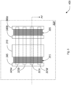
- Fig. 1 is a schematic top view of a GAA LDMOS FET 100 (hereinafter "LDMOS 100"), in accordance with various embodiments, in accordance with various embodiments.
- the LDMOS 100 includes a drain region 105, gate 110, and source region 115 disposed on a substrate 120.
- the LDMOS 100 further includes one or more first nanosheet stacks 125a-125d (collectively “the first nanosheet stacks 125”), one or more second nanosheet stacks 135a-135d (collectively “the second nanosheet stacks 135"), a first drain-side dummy gates 140a and second drain-side dummy gate 140b (collectively "the drain-side dummy gates 140), and source-side dummy gate 145.
- the various parts and components of LDMOS 100 are schematically illustrated in Fig. 1 , and that modifications to the various components and other arrangements of LDMOS 100 may be possible and in accordance with the various embodiments.
- the structures of the LDMOS 100 may be disposed on substrate 120.
- the substrate 120 may be a semiconductor substrate, such as, without limitation, bulk silicon.
- the substrate 120 includes a lightly doped ("p - " or "n - ”) silicon substrate.
- the substrate 120 may be lightly boron doped (e.g., p - ), in which well regions may be formed (e.g., p-well and n-well).
- the substrate 120 may further include more heavily doped ("p + " or "n + ”) regions, respectively doped with n-type (e.g., phosphorous) and p-type dopants (e.g., boron).
- a well refers to a doped region formed within the substrate 145, which serves as the "bulk” or “body” of the LDMOS 100, on (or in) which other parts of the device are formed, such as the drain region 105, gate 110, source region 115, first nanosheet stacks 125, second nanosheet stacks 135, drain side dummy gates 140, and source-side dummy gate 145.
- a "p-well” refers to a well with p-type doping
- an "n-well” refers to a well with n-type doping.
- boron and phosphorous are provided as non-limiting examples, and it is to be understood that in other embodiments, other dopants may be utilized.
- suitable dopants may include, without limitation, pentavalent atoms (e.g., arsenic, phosphorous, antimony, bismuth, lithium, etc.) for n-type doping and trivalent atoms (e.g., indium, aluminum, gallium, boron, etc.) for p-type doping.
- one or more first nanosheet stacks 125a-125d and one or more second nanosheet stacks 135a-135d may be disposed on the substrate 120.
- the one or more first nanosheet stacks 125a-125d and one or more second nanosheet stacks 135a-135d may only include a single respective nanosheet stack (e.g., one first nanosheet stack 125 and one second nanosheet stack 135).
- Nanosheet stacks may be formed using various processes, including, without limitation, growing and/or depositing the nanosheet stacks onto the substrate 120 (e.g., via an epitaxial process), forming the nanosheet stacks via lithography and/or etching, or a combination of processes.
- Nanosheets refer to two-dimensional sheet-like nanostructures, with thickness ranging from 1-100nm. In some examples, the nanosheet thickness may be in the range of 5-9nm, while in other examples, the nanosheet may be less than 5nm. The width and length of individual nanosheets may vary, as the dimensions may be determined based on the respective application. In various examples, the nanosheets may be referred to as having a length that extends in a "longitudinal direction,” and a width that extends in a "transverse direction”. Nanosheets may be formed of semiconducting material, as described above with respect to the substrate 120.
- a nanosheet stack refers to a stack of two or more nanosheets.
- the nanosheet stack may, in some examples, be referred to as being "vertically stacked," in which the nanosheets are disposed (e.g., stacked) over each other, above the "horizontal" plane defined by a top surface of the substrate 120.
- a nanosheet stack such as the first and second nanosheet stacks 125, 135, may be stacks of nanosheets formed by alternating semiconductor materials.
- the nanosheet stack may include alternating layers of silicon (Si) and silicon germanium (SiGe) nanosheets, where each layer refers to a respective type of nanosheet.
- the nanosheets may be formed from the same material as the substrate.
- each layer of the nanosheet may itself comprise one or more layers.
- a Si nanosheet layer may itself be formed from one or more layers of Si nanosheet.
- the Si nanosheet layer may be followed by a layer of SiGe which respectively comprises one or more layers of SiGe nanosheet.
- other materials may be utilized.
- individual nanosheet layers of the nanosheet stack may be separated by dielectric spacers, such as metal oxide spacers.
- the nanosheet stack may include alternating layers of different materials, such as a silicon nanosheet and a dielectric spacer.
- the nanosheet stack may include alternating layers of Si nanosheet and dielectric spacer.
- individual nanosheets may be configured to provide a respective channel between the gate 110 and source region 115.
- a channel between the drain and source regions 105, 115 (305, 315).
- nanosheet stacks are able to provide improved direct current (DC) performance and better control over short channel effects (SCE).
- DC direct current
- SCE short channel effects
- the gate 110, drain-side dummy gates 140a-140b, and source-side dummy gate 145 may then be formed by deposition of gate oxide (e.g., a dielectric layer) over the first and second nanosheet stacks 125, 135, followed by formation of the gate 110 and drain-side and source-side dummy gates 140a-140b, 145 from the gate oxide.
- gate oxide e.g., a dielectric layer
- the gate 110 and/or drain-side and source-side dummy gates 140a-140b, 145 may first be patterned and then deposited onto the substrate 120 and/or the first and second nanosheet stacks 125, 135.
- the physical dielectric structure of the gate 110 and/or gate electrode may be referred to as a "gate dielectric layer,” and the drain-side and source-side dummy gates 140a-140b, 145 may be referred to as "dummy dielectric layers.”
- Dummy gates refer to inactive gate structures used for various purposes.
- dummy gates may be used as structural support (as depicted in Figs. 2 and 4 to support the raised source / drain (RSD) epitaxial structures, and/or the first and second nanosheet stacks 125, 135), electrical biasing, electrical isolation, and/or as a placeholder structure to later be removed or replaced.
- RSD raised source / drain
- the drain region 105 may be disposed on a first side of the gate 110, between the drain side dummy gates 140a-140b.
- the drain region 105 includes a highly doped part of the first nanosheet stacks 125.
- the first nanosheet stacks 125 may include a highly doped portion that is doped in-situ to form at least part of the drain region 105.
- all or part of the first nanosheet stacks 125 may be in-situ phosphorous doped.
- the nanosheets may be undoped nanosheets.
- an RSD epitaxial layer (hereinafter referred to as "epitaxial layer”) may be formed over the nanosheet stacks.
- the epitaxial layer may refer to a structure / layer grown via an epitaxial process.
- the epitaxial layer may form, at least part, of an RSD.
- the epitaxial layer may be heavily doped, forming the drain structure (also referred to as "drain/source") of the drain region 105.
- the drain region 105 may be referred to interchangeably as the "drain” or “drain/source” of the LDMOS 100.
- the epitaxial layer may be configured to connect transversely the one or more first nanosheet stacks 125a-125d to one another.
- the epitaxial layer may extend longitudinally, such that the epitaxial layer traverses the one or more first nanosheet stacks 125a-125d, as depicted in Fig. 1 .
- the source region 115 may be disposed on a second side of the gate 110 (e.g., opposite from the first side of the gate 110).
- the source region 115 is disposed between source-side dummy gate 145 and the gate 110.
- the source region 115 may include a highly doped portion of the second nanosheet stacks 135.
- the second nanosheet stacks 135 may include a first highly doped portion that is doped in-situ to form at least part of the source region 115.
- a first portion of the second nanosheet stacks 135 may be in-situ phosphorous doped.
- the nanosheets of the second nanosheet stack may be undoped.
- a source-side epitaxial layer may be formed over the second nanosheet stacks 135, forming the source (also referred to as a "source/drain"), as part or in addition to the in-situ doping process.
- the source region 115 may be referred to interchangeably as the "source” or “source/drain” of the LDMOS 100.
- the source-side epitaxial layer may be configured to connect transversely the one or more second nanosheet stacks 135a-135d to one another.
- the epitaxial layer of the source region 115 may extend in a longitudinal direction such that it traverses the one or more second nanosheet stacks 135a-135d, extending in a longitudinal direction, as depicted in Fig. 1 .
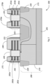
- Fig. 2 is a schematic diagram of a cross-section of the LDMOS 100, 200 taken across line x-x, in accordance with various embodiments.
- the sectional view of LDMOS 200 shows the different portions and structures described above, but obscured in the top view.
- LDMOS 200 includes a substrate 280, having an undoped/lightly doped region 205, a first well region 210, and second well region 215, a first trench isolation region 220, second trench isolation region 225, and third trench isolation region 230, drain region 235, gate 240, source region 245, first nanosheet stack 255, second nanosheet stack 265, drain-side dummy gates 270a-270b, and source-side dummy gates 275.
- the various parts and components of LDMOS 200 are schematically illustrated in Fig. 2 , and that modifications to the various components and other arrangements of LDMOS 200 may be possible and in accordance with the various embodiments.
- the substrate 280 may include an undoped/lightly doped region 205.
- the substrate 280 may be lightly doped.
- the undoped/lightly doped region 205 is lightly boron doped (e.g., p-type).
- the substrate 280 further includes a first well region 210 and second well region 215.
- the well regions 210, 215 may be doped regions of the substrate 280.
- the first well region 210 may be p-type doped (e.g., boron doped)
- the second well region 215 may be n-type doped (e.g., phosphorous doped).
- the substrate 280 further includes trench isolation regions, such as first through third trench isolation regions 220-230.
- Trench isolation regions may be trenches formed in the substrate, and filled with an oxide material.
- one or more of the first, second, and third trench isolation regions 220-230 may be shallow trench isolation (STI) regions.
- one or more of the first, second, and third trench isolation regions 220-230 may be deep trench isolation (DTI) regions.
- STI shallow trench isolation
- DTI deep trench isolation
- the first and second nanosheet stacks 255, 265 may be disposed on the substrate 280, with the first nanosheet stack 255 disposed on the second well region 215, and the second nanosheet stack 265 at least partially disposed on the first well region 210, and at least partially disposed on the second well region 215.
- the second nanosheet stack 265 may act as channels for current flow between gate and source.
- the first nanosheet stack 255 may, in turn, provide greater effective width as compared to a fin, allowing for higher drive currents.
- the drain region may be disposed between the third trench isolation region 230 and second trench isolation region 225, with the respective nanosheets 255a-255c of the first nanosheet stack 225 disposed, at least partially, over and spanning between the second and third trench isolation regions 225, 230.
- a lightly-doped drain (LDD) region may be formed directly under the drain region 230 in the second well region 215 between the second and third trench isolation regions 225, 230, creating a current path from the drain region 235, through the second well region 215, to the drain region 245.
- LDD lightly-doped drain
- Fig. 3 is a schematic top view of an alternative configuration for a GAA LDMOS FET 300 (hereinafter "LDMOS 300"), in accordance with various embodiments, in accordance with various embodiments.
- the LDMOS 300 includes a drain region 305, gate 310, and source region 315 disposed on a substrate 320.
- the LDMOS 300 further includes one or more nanosheet stacks 325a-325d (collectively " nanosheet stacks 325"), a first drain-side dummy gates 340a and second drain-side dummy gate 340b (collectively "the drain-side dummy gates 340), and source-side dummy gate 345.
- the various parts and components of LDMOS 300 are schematically illustrated in Fig. 3 , and that modifications to the various components and other arrangements of LDMOS 300 may be possible and in accordance with the various embodiments.
- the structures of the LDMOS 300 may be disposed on substrate 320.
- the substrate 320 may be a semiconductor substrate, such as, without limitation, bulk silicon.
- the one or more nanosheet stacks 325a-325d may be disposed on the substrate 320.
- the one or more nanosheet stacks may only include a single nanosheet stack (e.g., one nanosheet stack 325).
- the nanosheet stacks 325 may be stacks of nanosheets formed by alternating semiconductor materials, as previously described. In yet further examples, the nanosheets may be formed from the same material as the substrate. In yet further examples, the nanosheet stack 325 may be formed from alternating layers of nanosheets and spacers. As previously described, individual nanosheet layers of the nanosheet stack 325 may be separated by dielectric spacers, such as metal oxide spacers.
- the nanosheets of the nanosheet stacks 325 of LDMOS 300 spans across the drain region 305, gate 310, and source region 315.
- the nanosheets may be continuous (e.g., are structurally continuous) from the first drain-side dummy gate 340 (e.g., disposed at least partially within the first dummy gate 340) to the source-side dummy gate 345.
- individual nanosheets may be configured to provide respective channels from the source region 305 to the source region 315 (e.g., more specifically, from the drain region 305 to the gate 310, and from the gate 310 to the source region 315).
- the gate 310, drain-side dummy gates 340a-340b, and source-side dummy gate 345 may then be formed by deposition of gate oxide (e.g., a dielectric layer) over the nanosheet stacks 325, followed by formation of the gate 310 and drain-side and source-side dummy gates 340a-340b, 345 from the gate oxide.
- the drain region 305 may be disposed on a first side of the gate 310, between the drain side dummy gates 340a-340b.
- the drain region 305 includes a highly doped part of the nanosheet stacks 325.
- the nanosheet stacks 325 may include a highly doped portion that is doped in-situ to form at least part of the drain region 305. In some examples, in the case of an NLDMOS, all or part of the nanosheet stacks 325 may be in-situ phosphorous doped. In other examples, the nanosheets may be undoped nanosheets.
- an RSD epitaxial layer (hereinafter referred to as “epitaxial layer”) may be formed over the nanosheet stacks.
- the epitaxial layer may be heavily doped, forming the drain structure (also referred to as “drain/source”) of the drain region 305.
- the epitaxial layer may be configured to connect transversely the one or more nanosheet stacks 325a-325d to one another.
- the source region 315 may be disposed on a second side of the gate 310 (e.g., opposite from the first side of the gate 310).
- the source region 315 is disposed between source-side dummy gate 345 and the gate 310.
- the source region 315 may include a highly doped portion of the nanosheet stacks 325.
- the nanosheet stacks 325 may include a first highly doped portion that is doped in-situ to form at least part of the source region 315.
- a first portion of the nanosheet stacks 325 may be in-situ phosphorous doped.
- the nanosheets of the second nanosheet stack may be undoped.
- a source-side epitaxial layer (e.g., RSD epitaxial layer) may be formed over the nanosheet stacks 325, forming the source (also referred to as a "source/drain"), as part or in addition to the in-situ doping process.
- the source-side epitaxial layer may be configured to connect transversely the one or more nanosheet stacks 325a-325d to one another.
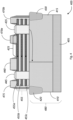
- Fig. 4 is a schematic diagram of a cross-section of the LDMOS 300, 400 taken across line 1-1, in accordance with various embodiments.
- the sectional view of LDMOS 400 shows the different portions and structures described above, but obscured in the top view.
- LDMOS 400 includes a substrate 480, having an undoped/lightly doped region 405, a first well region 410, and second well region 415, a first trench isolation region 420, LDD region 425, and second trench isolation region 430, drain region 435, gate 440, source region 445, nanosheet stack 455, drain-side dummy gates 470a-470b, and source-side dummy gates 475.
- the various parts and components of LDMOS 400 are schematically illustrated in Fig. 4 , and that modifications to the various components and other arrangements of LDMOS 400 may be possible and in accordance with the various embodiments.
- LDMOS 400 includes a first and second trench isolation regions, such as first and second trench isolation regions 420, 430, the first trench isolation region 420 disposed at one end of the first well region 410, and second trench isolation region 430 disposed at the opposite end of the second well region 415.
- a trench isolation region between the first and second trench isolation regions 420, 430 has been removed in favor of an LDD region 425 formed in the area between the gate 440 and source region 435.
- trench isolation regions may be trenches formed in the substrate, and filled with an oxide material.
- One or more of the first and second trench isolation regions 420, 430 may be shallow trench isolation (STI) regions.
- one or more of the first and second trench isolation regions 420, 430 may be deep trench isolation (DTI) regions.
- STI shallow trench isolation
- DTI deep trench isolation
- the nanosheet stacks 455 may be disposed on the substrate 480, extending across the first and second well regions 410, 415.
- the individual nanosheets 455a-455c of the nanosheet stacks 455 may be channels for current flow between drain and gate, and further between the gate and source.
- a current path is created through the nanosheets 455a-455c, as well as through the second well region 415.
- an LDD region through the nanosheet stack 455.
- R on reduced on resistance
Landscapes
- Engineering & Computer Science (AREA)
- Chemical & Material Sciences (AREA)
- Nanotechnology (AREA)
- Physics & Mathematics (AREA)
- Mathematical Physics (AREA)
- Theoretical Computer Science (AREA)
- Crystallography & Structural Chemistry (AREA)
- Insulated Gate Type Field-Effect Transistor (AREA)
Applications Claiming Priority (1)
| Application Number | Priority Date | Filing Date | Title |
|---|---|---|---|
| US18/361,776 US20250040169A1 (en) | 2023-07-28 | 2023-07-28 | Gate All-Around Laterally Diffused Metal-Oxide Semiconductor Field Effect Transistor |
Publications (2)
| Publication Number | Publication Date |
|---|---|
| EP4498435A2 true EP4498435A2 (de) | 2025-01-29 |
| EP4498435A3 EP4498435A3 (de) | 2025-06-11 |
Family
ID=92043335
Family Applications (1)
| Application Number | Title | Priority Date | Filing Date |
|---|---|---|---|
| EP24190973.8A Pending EP4498435A3 (de) | 2023-07-28 | 2024-07-25 | Gate-all-around-feldeffekttransistor mit seitlich diffundiertem metalloxidhalbleiter |
Country Status (3)
| Country | Link |
|---|---|
| US (1) | US20250040169A1 (de) |
| EP (1) | EP4498435A3 (de) |
| CN (1) | CN119486200A (de) |
Cited By (1)
| Publication number | Priority date | Publication date | Assignee | Title |
|---|---|---|---|---|
| EP4723828A1 (de) * | 2024-10-07 | 2026-04-08 | Avago Technologies International Sales Pte. Limited | Halbleiterbauelemente mit gemischtem kanal |
Citations (1)
| Publication number | Priority date | Publication date | Assignee | Title |
|---|---|---|---|---|
| US20220262948A1 (en) * | 2019-10-08 | 2022-08-18 | Csmc Technologies Fab2 Co., Ltd. | Ldmos device and method for preparing same |
Family Cites Families (21)
| Publication number | Priority date | Publication date | Assignee | Title |
|---|---|---|---|---|
| US20160071729A1 (en) * | 2014-09-04 | 2016-03-10 | Samsung Electronics Co., Ltd. | Rectangular nanosheet fabrication |
| CN106960870B (zh) * | 2016-01-11 | 2021-09-10 | 三星电子株式会社 | 半导体装置及其制造方法 |
| US10505020B2 (en) * | 2016-10-13 | 2019-12-10 | Avago Technologies International Sales Pte. Limited | FinFET LDMOS devices with improved reliability |
| US10332965B2 (en) * | 2017-05-08 | 2019-06-25 | Taiwan Semiconductor Manufacturing Co., Ltd. | Semiconductor device and method of fabricating the same |
| US10439049B2 (en) * | 2017-12-19 | 2019-10-08 | International Business Machines Corporation | Nanosheet device with close source drain proximity |
| US10679890B2 (en) * | 2018-02-01 | 2020-06-09 | International Business Machines Corporation | Nanosheet structure with isolated gate |
| US10679906B2 (en) * | 2018-07-17 | 2020-06-09 | International Business Machines Corporation | Method of forming nanosheet transistor structures with reduced parasitic capacitance and improved junction sharpness |
| US11031397B2 (en) * | 2018-09-27 | 2021-06-08 | Taiwan Semiconductor Manufacturing Co., Ltd. | Multi-gate device integration with separated Fin-like field effect transistor cells and gate-all-around transistor cells |
| US11527612B2 (en) * | 2018-09-28 | 2022-12-13 | Intel Corporation | Gate-all-around integrated circuit structures having vertically discrete source or drain structures |
| US11195911B2 (en) * | 2019-12-23 | 2021-12-07 | International Business Machines Corporation | Bottom dielectric isolation structure for nanosheet containing devices |
| US11094782B1 (en) * | 2020-02-19 | 2021-08-17 | Intel Corporation | Gate-all-around integrated circuit structures having depopulated channel structures |
| DE102021108221A1 (de) * | 2020-05-26 | 2021-12-02 | Taiwan Semiconductor Manufacturing Co., Ltd. | Kanalkonfiguration zur Verbesserung der Leistung eines Multigate-Bauelements und Verfahren zur Fertigung davon |
| KR102840435B1 (ko) * | 2020-12-16 | 2025-07-29 | 삼성전자주식회사 | 반도체 장치 |
| US11659703B2 (en) * | 2021-02-26 | 2023-05-23 | Taiwan Semiconductor Manufacturing Company, Ltd. | Integrated circuit with embedded high-density and high-current SRAM macros |
| US12532504B2 (en) * | 2021-07-30 | 2026-01-20 | Taiwan Semiconductor Manufacturing Company, Ltd. | Device structure with reduced leakage current |
| US12062692B2 (en) * | 2021-08-27 | 2024-08-13 | Taiwan Semiconductor Manufacturing Company, Ltd. | Tapered dielectric layer for preventing electrical shorting between gate and back side via |
| US12477712B2 (en) * | 2022-05-18 | 2025-11-18 | Taiwan Semiconductor Manufacturing Company, Ltd. | Memory structure and method for manufacturing the same |
| US12419026B2 (en) * | 2022-06-29 | 2025-09-16 | Taiwan Semiconductor Manufacturing Company, Ltd. | Memory structure |
| US20240243133A1 (en) * | 2023-01-17 | 2024-07-18 | Taiwan Semiconductor Manufacturing Company, Ltd. | Semiconductor structure and method for manufacturing the same |
| US20240413239A1 (en) * | 2023-06-09 | 2024-12-12 | Texas Instruments Incorporated | Ldmos nanosheet transistor |
| US20240431089A1 (en) * | 2023-06-21 | 2024-12-26 | Taiwan Semiconductor Manufacturing Company, Ltd. | Memory device |
-
2023
- 2023-07-28 US US18/361,776 patent/US20250040169A1/en active Pending
-
2024
- 2024-05-30 CN CN202410686092.7A patent/CN119486200A/zh active Pending
- 2024-07-25 EP EP24190973.8A patent/EP4498435A3/de active Pending
Patent Citations (1)
| Publication number | Priority date | Publication date | Assignee | Title |
|---|---|---|---|---|
| US20220262948A1 (en) * | 2019-10-08 | 2022-08-18 | Csmc Technologies Fab2 Co., Ltd. | Ldmos device and method for preparing same |
Cited By (1)
| Publication number | Priority date | Publication date | Assignee | Title |
|---|---|---|---|---|
| EP4723828A1 (de) * | 2024-10-07 | 2026-04-08 | Avago Technologies International Sales Pte. Limited | Halbleiterbauelemente mit gemischtem kanal |
Also Published As
| Publication number | Publication date |
|---|---|
| EP4498435A3 (de) | 2025-06-11 |
| CN119486200A (zh) | 2025-02-18 |
| US20250040169A1 (en) | 2025-01-30 |
Similar Documents
| Publication | Publication Date | Title |
|---|---|---|
| US9698060B2 (en) | Germanium FinFETs with metal gates and stressors | |
| US11367662B2 (en) | Semiconductor devices and methods of forming the same | |
| US12245442B2 (en) | Semiconductor device, method of manufacturing the same and electronic device including the same | |
| US7692254B2 (en) | Fin-type field effect transistor structure with merged source/drain silicide and method of forming the structure | |
| US8609499B2 (en) | FinFETs and the methods for forming the same | |
| US8759184B2 (en) | FinFETs and the methods for forming the same | |
| US8796759B2 (en) | Fin-like field effect transistor (FinFET) device and method of manufacturing same | |
| US8735993B2 (en) | FinFET body contact and method of making same | |
| US20150255456A1 (en) | Replacement fin insolation in a semiconductor device | |
| US9691763B2 (en) | Multi-gate FinFET semiconductor device with flexible design width | |
| JP5645368B2 (ja) | 半導体装置およびその製造方法 | |
| CN111584486A (zh) | 具有交错结构的半导体装置及其制造方法及电子设备 | |
| US8847324B2 (en) | Increasing ION /IOFF ratio in FinFETs and nano-wires | |
| US8350269B2 (en) | Semiconductor-on-insulator (SOI) structure and method of forming the SOI structure using a bulk semiconductor starting wafer | |
| US10128244B2 (en) | CMOS devices having charged punch-through stopper layer to reduce punch-through and methods of manufacturing the same | |
| CN105185712B (zh) | 包括鳍式场效应晶体管的集成电路器件及其形成方法 | |
| EP4498435A2 (de) | Gate-all-around-feldeffekttransistor mit seitlich diffundiertem metalloxidhalbleiter | |
| EP4152371A1 (de) | Fin-basierte feldeffekttransistorvorrichtung mit verbessertem anschaltwiderstand und verbesserter durchbruchspannung | |
| US20180040697A1 (en) | Fully depleted silicon-on-insulator device formation | |
| EP4557908A1 (de) | Flächeneffizienter fin-basierter lateral-diffundierter metalloxid-halbleiter-feldeffekttransistor | |
| EP4503135A1 (de) | Lateral-diffundierte metalloxid-halbleiterbauelemente mit verringerter gate-ladung und zeitabhängigem dielektrischem durchbruch | |
| CN106876393B (zh) | 半导体器件及其形成方法 | |
| CN121751683A (zh) | 半导体结构 |
Legal Events
| Date | Code | Title | Description |
|---|---|---|---|
| PUAI | Public reference made under article 153(3) epc to a published international application that has entered the european phase |
Free format text: ORIGINAL CODE: 0009012 |
|
| STAA | Information on the status of an ep patent application or granted ep patent |
Free format text: STATUS: THE APPLICATION HAS BEEN PUBLISHED |
|
| AK | Designated contracting states |
Kind code of ref document: A2 Designated state(s): AL AT BE BG CH CY CZ DE DK EE ES FI FR GB GR HR HU IE IS IT LI LT LU LV MC ME MK MT NL NO PL PT RO RS SE SI SK SM TR |
|
| REG | Reference to a national code |
Ref country code: DE Ref legal event code: R079 Free format text: PREVIOUS MAIN CLASS: H01L0029060000 Ipc: H10D0062100000 |
|
| RIC1 | Information provided on ipc code assigned before grant |
Ipc: H10D 62/17 20250101ALN20250212BHEP Ipc: H10D 62/13 20250101ALI20250212BHEP Ipc: H10D 30/67 20250101ALI20250212BHEP Ipc: H10D 84/83 20250101ALI20250212BHEP Ipc: H10D 84/01 20250101ALI20250212BHEP Ipc: H10D 30/65 20250101ALI20250212BHEP Ipc: H10D 30/43 20250101ALI20250212BHEP Ipc: H10D 64/00 20250101ALI20250212BHEP Ipc: H10D 62/10 20250101AFI20250212BHEP |
|
| PUAL | Search report despatched |
Free format text: ORIGINAL CODE: 0009013 |
|
| AK | Designated contracting states |
Kind code of ref document: A3 Designated state(s): AL AT BE BG CH CY CZ DE DK EE ES FI FR GB GR HR HU IE IS IT LI LT LU LV MC ME MK MT NL NO PL PT RO RS SE SI SK SM TR |
|
| RIC1 | Information provided on ipc code assigned before grant |
Ipc: H10D 62/17 20250101ALN20250507BHEP Ipc: H10D 62/13 20250101ALI20250507BHEP Ipc: H10D 30/67 20250101ALI20250507BHEP Ipc: H10D 84/83 20250101ALI20250507BHEP Ipc: H10D 84/01 20250101ALI20250507BHEP Ipc: H10D 30/65 20250101ALI20250507BHEP Ipc: H10D 30/43 20250101ALI20250507BHEP Ipc: H10D 64/00 20250101ALI20250507BHEP Ipc: H10D 62/10 20250101AFI20250507BHEP |
|
| STAA | Information on the status of an ep patent application or granted ep patent |
Free format text: STATUS: REQUEST FOR EXAMINATION WAS MADE |
|
| 17P | Request for examination filed |
Effective date: 20251211 |