EP4496458A2 - Metallkomplexe von 3-(2,3,5-trifluor-6-(trifluormethyl)pyridin-4-yl)pentan-2,4-dion und ähnlichen liganden als halbleitermaterialien zur verwendung in elektronischen vorrichtungen - Google Patents
Metallkomplexe von 3-(2,3,5-trifluor-6-(trifluormethyl)pyridin-4-yl)pentan-2,4-dion und ähnlichen liganden als halbleitermaterialien zur verwendung in elektronischen vorrichtungen Download PDFInfo
- Publication number
- EP4496458A2 EP4496458A2 EP24208778.1A EP24208778A EP4496458A2 EP 4496458 A2 EP4496458 A2 EP 4496458A2 EP 24208778 A EP24208778 A EP 24208778A EP 4496458 A2 EP4496458 A2 EP 4496458A2
- Authority
- EP
- European Patent Office
- Prior art keywords
- substituted
- unsubstituted
- alkyl
- iii
- compound
- Prior art date
- Legal status (The legal status is an assumption and is not a legal conclusion. Google has not performed a legal analysis and makes no representation as to the accuracy of the status listed.)
- Pending
Links
Images

Classifications
-
- C—CHEMISTRY; METALLURGY
- C07—ORGANIC CHEMISTRY
- C07D—HETEROCYCLIC COMPOUNDS
- C07D213/00—Heterocyclic compounds containing six-membered rings, not condensed with other rings, with one nitrogen atom as the only ring hetero atom and three or more double bonds between ring members or between ring members and non-ring members
- C07D213/02—Heterocyclic compounds containing six-membered rings, not condensed with other rings, with one nitrogen atom as the only ring hetero atom and three or more double bonds between ring members or between ring members and non-ring members having three double bonds between ring members or between ring members and non-ring members
- C07D213/04—Heterocyclic compounds containing six-membered rings, not condensed with other rings, with one nitrogen atom as the only ring hetero atom and three or more double bonds between ring members or between ring members and non-ring members having three double bonds between ring members or between ring members and non-ring members having no bond between the ring nitrogen atom and a non-ring member or having only hydrogen or carbon atoms directly attached to the ring nitrogen atom
- C07D213/60—Heterocyclic compounds containing six-membered rings, not condensed with other rings, with one nitrogen atom as the only ring hetero atom and three or more double bonds between ring members or between ring members and non-ring members having three double bonds between ring members or between ring members and non-ring members having no bond between the ring nitrogen atom and a non-ring member or having only hydrogen or carbon atoms directly attached to the ring nitrogen atom with hetero atoms or with carbon atoms having three bonds to hetero atoms with at the most one bond to halogen, e.g. ester or nitrile radicals, directly attached to ring carbon atoms
- C07D213/61—Halogen atoms or nitro radicals
-
- C—CHEMISTRY; METALLURGY
- C07—ORGANIC CHEMISTRY
- C07D—HETEROCYCLIC COMPOUNDS
- C07D209/00—Heterocyclic compounds containing five-membered rings, condensed with other rings, with one nitrogen atom as the only ring hetero atom
- C07D209/56—Ring systems containing three or more rings
- C07D209/80—[b, c]- or [b, d]-condensed
- C07D209/82—Carbazoles; Hydrogenated carbazoles
- C07D209/86—Carbazoles; Hydrogenated carbazoles with only hydrogen atoms, hydrocarbon or substituted hydrocarbon radicals, directly attached to carbon atoms of the ring system
-
- C—CHEMISTRY; METALLURGY
- C09—DYES; PAINTS; POLISHES; NATURAL RESINS; ADHESIVES; COMPOSITIONS NOT OTHERWISE PROVIDED FOR; APPLICATIONS OF MATERIALS NOT OTHERWISE PROVIDED FOR
- C09B—ORGANIC DYES OR CLOSELY-RELATED COMPOUNDS FOR PRODUCING DYES, e.g. PIGMENTS; MORDANTS; LAKES
- C09B57/00—Other synthetic dyes of known constitution
- C09B57/10—Metal complexes of organic compounds not being dyes in uncomplexed form
-
- H—ELECTRICITY
- H10—SEMICONDUCTOR DEVICES; ELECTRIC SOLID-STATE DEVICES NOT OTHERWISE PROVIDED FOR
- H10K—ORGANIC ELECTRIC SOLID-STATE DEVICES
- H10K85/00—Organic materials used in the body or electrodes of devices covered by this subclass
- H10K85/30—Coordination compounds
- H10K85/331—Metal complexes comprising an iron-series metal, e.g. Fe, Co, Ni
-
- H—ELECTRICITY
- H10—SEMICONDUCTOR DEVICES; ELECTRIC SOLID-STATE DEVICES NOT OTHERWISE PROVIDED FOR
- H10K—ORGANIC ELECTRIC SOLID-STATE DEVICES
- H10K85/00—Organic materials used in the body or electrodes of devices covered by this subclass
- H10K85/30—Coordination compounds
- H10K85/371—Metal complexes comprising a group IB metal element, e.g. comprising copper, gold or silver
-
- H—ELECTRICITY
- H10—SEMICONDUCTOR DEVICES; ELECTRIC SOLID-STATE DEVICES NOT OTHERWISE PROVIDED FOR
- H10K—ORGANIC ELECTRIC SOLID-STATE DEVICES
- H10K50/00—Organic light-emitting devices
- H10K50/10—OLEDs or polymer light-emitting diodes [PLED]
- H10K50/14—Carrier transporting layers
- H10K50/15—Hole transporting layers
-
- Y—GENERAL TAGGING OF NEW TECHNOLOGICAL DEVELOPMENTS; GENERAL TAGGING OF CROSS-SECTIONAL TECHNOLOGIES SPANNING OVER SEVERAL SECTIONS OF THE IPC; TECHNICAL SUBJECTS COVERED BY FORMER USPC CROSS-REFERENCE ART COLLECTIONS [XRACs] AND DIGESTS
- Y02—TECHNOLOGIES OR APPLICATIONS FOR MITIGATION OR ADAPTATION AGAINST CLIMATE CHANGE
- Y02E—REDUCTION OF GREENHOUSE GAS [GHG] EMISSIONS, RELATED TO ENERGY GENERATION, TRANSMISSION OR DISTRIBUTION
- Y02E10/00—Energy generation through renewable energy sources
- Y02E10/50—Photovoltaic [PV] energy
- Y02E10/549—Organic PV cells
Definitions
- the present invention relates to a compound of formula (I), a semiconductor material comprising at least one compound of formula (I), an semiconductor layer comprising at least one compound of formula (I) and an electronic device comprising at least one compound of formula (I).
- OLEDs organic light-emitting diodes
- a typical OLED comprises an anode layer, a hole injection layer HIL, a hole transport layer HTL, an emission layer EML, an electron transport layer ETL, and a cathode layer, which are sequentially stacked on a substrate.
- the HIL, the HTL, the EML, and the ETL are thin films formed from organic compounds.
- Performance of an organic light emitting diode may be affected by characteristics of the hole injection layer, and among them, may be affected by characteristics of the hole transport compound and the metal complexes which are contained in the hole injection layer.
- WO16188604 A1 relates to a composition at least one hole-transport or/and one hole-injection material and at least one metal complex as a p-dopant.
- An aspect of the present invention provides a compound represented by Formula I: wherein
- substituted refers to a substituted selected from halogen, F, Cl, CN, substituted or unsubstituted C 1 to C 6 alkyl, partially or fully fluorinated C 1 to C 6 alkyl, substituted or unsubstituted C 1 to C 6 alkoxy, partially or fully fluorinated C 1 to C 6 alkoxy, substituted or unsubstituted C 6 to C 18 aryl, and substituted or unsubstituted C 2 to C 18 heteroaryl, wherein the substituents are selected from halogen, F, Cl, CN, C 1 to C 6 alkyl, CF 3 , OCH 3 and OCF 3 .
- aryl group and “aromatic rings” refers to a hydrocarbyl group which may be created by formal abstraction of one hydrogen atom from an aromatic ring in the corresponding aromatic hydrocarbon.
- Aromatic hydrocarbon refers to a hydrocarbon which contains at least one aromatic ring or aromatic ring system.
- Aromatic ring or aromatic ring system refers to a planar ring or ring system of covalently bound carbon atoms, wherein the planar ring or ring system comprises a conjugated system of delocalized electrons fulfilling Hückel's rule.
- aryl groups include monocyclic groups like phenyl or tolyl, polycyclic groups which comprise more aromatic rings linked by single bonds, like biphenyl, and polycyclic groups comprising fused rings, like naphthyl or fluorenyl.
- non-heterocycle is understood to mean a ring or ring-system comprising no hetero-atom as a ring member.
- heterocycle is understood to mean that the heterocycle comprises at least one ring comprising one or more hetero-atoms.
- a heterocycle comprising more than one ring means that all rings comprising a hetero-atom or at least one ring comprising a hetero atom and at least one ring comprising C-atoms only and no hetero atom.
- heterocycloalkyl it is especially where suitable understood a group derived by formal abstraction of one ring hydrogen from a saturated cycloalkyl ring in a compound comprising at least one such ring.
- aryl having at least 9 C-atoms may comprise at least one fused aryl ring.
- heteroaryl having at least 9 atoms may comprise at least one fused heteroaryl ring fused with a heteroaryl ring or fused with an aryl ring.
- fused aryl rings or “condensed aryl rings” is understood the way that two aryl rings are considered fused or condensed when they share at least two common sp 2 -hybridized carbon atoms.
- fused ring system is understood to mean a ring system wherein two or more rings share at least two atoms.
- 5-, 6- or 7-member ring is understood to mean a ring comprising 5, 6 or 7 atoms.
- the atoms may be selected from C and one or more hetero-atoms.
- the single bond refers to a direct bond.
- a "substituted alkyl group” may refer to a linear, branched or cyclic substituted saturated aliphatic hydrocarbyl group.
- the substituted alkyl group may be a linear, branched or cyclic C 1 to C 12 alkyl group. More specifically, the substituted alkyl group may be a linear, branched or cyclic substituted C 1 to C 10 alkyl group or a linear, branched or cyclic substituted C 1 to C 6 alkyl group.
- hetero is understood the way that at least one carbon atom, in a structure which may be formed by covalently bound carbon atoms, is replaced by another polyvalent atom.
- the heteroatoms are selected from B, Si, N, P, O, S; further preferred from N, P, O, S and most preferred N.
- contacting sandwiched refers to an arrangement of three layers whereby the layer in the middle is in direct contact with the two adjacent layers.
- OLED organic light-emitting diode
- organic light-emitting device organic light-emitting device
- anode anode layer and anode electrode are used synonymously.
- At least two anode sub-layers is understood to mean two or more anode sub-layers, for example two or three anode sub-layers.
- hole injection layer is understood to mean a layer which improves charge injection from the anode layer into further layers in the electronic device or from further layers of the electronic device into the anode.
- R 1 , R 2 are selected from unsubstituted C 1 to C 12 alkyl, preferably CH 3 , or a substituted 6-member heteroaryl ring with 1, 2 or 3 N atoms and the remaining atoms are C, wherein the at least one substituent is selected from F, CN, CF 3 ; wherein R 1 or R 2 is selected from a 6 member heteroaryl ring with 1, 2 or 3 N atoms and the remaining atoms are C, wherein at least three of the remaining C-atoms of the heteroaryl ring are substituent with a substituent individually selected from the group halogen, F, Cl, CN, CF 3 , preferably F, CN, CF 3 ; and R 3 is CH 3 , CF 3 , CN preferably CH 3 or CF 3 .
- R 1 , R 2 are selected from unsubstituted C 1 to C 12 alkyl, preferably CH 3 , or a substituted 6-member heteroaryl ring with 1, 2 or 3 N atoms and the remaining atoms are C, wherein the at least one substituent is selected from F, CN, CF 3 ; wherein R 1 or R 2 is selected from a 6 member heteroaryl ring with 1 or 2 N atoms and the remaining atoms are C, wherein at least four of the remaining C-atoms of the heteroaryl ring are substituent with a substituent individually selected from the group halogen, F, Cl, CN, CF 3 , preferably F, CN, CF 3 ; and R 3 is CH 3 , CF 3 , CN preferably CH 3 or CF 3 .
- the at least one substituent on the C 2 to C 24 heteroaryl group is selected from F, CN, partially or fully fluorinated C 1 to C 6 alkyl; more preferred F, CN, partially or fully fluorinated C 1 to C 6 alkyl, also preferred halogen, F, Cl, CN, partially or fully fluorinated C 1 to C 4 alkyl.
- At least one substituted C 2 to C 24 heteroaryl group of R 1 , R 2 or R 3 is selected from the following Formulas D1 to D29: wherein the "*" denotes the binding position.
- the covalent matrix compound is free of metal atoms and majority of its skeletal atoms may be selected from C and N, preferably the covalent matrix compound is free of metal atoms and majority of its skeletal atoms may be selected from C and the minority of its skeletal atoms may be N.
- the substantially covalent matrix compound may have a molecular weight Mw of ⁇ 400 and ⁇ 2000 g/mol, preferably a molecular weight Mw of ⁇ 450 and ⁇ 1500 g/mol, further preferred a molecular weight Mw of ⁇ 500 and ⁇ 1000 g/mol, in addition preferred a molecular weight Mw of ⁇ 550 and ⁇ 900 g/mol, also preferred a molecular weight Mw of ⁇ 600 and ⁇ 800 g/mol.
- the HOMO level of the substantially covalent matrix compound may be more negative than the HOMO level of N2,N2,N2',N2',N7,N7,N7',N7'-octakis(4-methoxyphenyl)-9,9'-spirobi[fluorene]-2,2',7,7'-tetraamine ( CAS 207739-72-8 ) when determined under the same conditions.
- the substantially covalent matrix compound may be free of alkoxy groups.
- Ar 1 , Ar 2 , Ar 3 , Ar 4 and Ar 5 may be independently selected from the group consisting of B1, B2, B5, B7, B9, B10, B13 to B16.
- the compound of formula (III) or formula (IV) may comprises at least ⁇ 1 to ⁇ 6 substituted or unsubstituted aromatic fused ring systems comprising heteroaromatic rings.
- the compound of formula (III) or formula (IV) may comprises at least ⁇ 1 to ⁇ 6 substituted or unsubstituted aromatic fused ring systems comprising heteroaromatic rings and at least ⁇ 1 to ⁇ 3 substituted or unsubstituted unsaturated 5- to 7-member ring of a heterocycle, preferably ⁇ 2 to ⁇ 5 substituted or unsubstituted aromatic fused ring systems comprising heteroaromatic rings.
- the compound of formula (III) or formula (IV) may comprises at least ⁇ 1 to ⁇ 6 substituted or unsubstituted aromatic fused ring systems, preferably ⁇ 2 to ⁇ 5 substituted or unsubstituted aromatic fused ring systems, and further preferred 3 or 4 substituted or unsubstituted aromatic fused ring systems.
- the compound of formula (III) or formula (IV) may comprises at least ⁇ 1 to ⁇ 6 substituted or unsubstituted aromatic fused ring systems, preferably ⁇ 2 to ⁇ 5 substituted or unsubstituted aromatic fused ring systems, and further preferred 3 or 4 substituted or unsubstituted aromatic fused ring systems, which comprises substituted or unsubstituted heteroaromatic rings.
- the compound of formula (III) or formula (IV) may comprises at least ⁇ 1 to ⁇ 3 or 2 substituted or unsubstituted unsaturated 5- to 7-member ring of a heterocycle.
- the compound of formula (III) or formula (IV) may comprises at least ⁇ 1 to ⁇ 3 or 2 substituted or unsubstituted unsaturated 7-member ring of a heterocycle.
- substituted or unsubstituted aromatic fused ring systems of the compound of formula (III) or formula (IV) may comprises at least ⁇ 1 to ⁇ 3 or 2 substituted or unsubstituted unsaturated 5- to 7-member ring of a heterocycle.
- the substituted or unsubstituted aromatic fused ring systems of the matrix compound of formula (III) or formula (IV) may comprises at least ⁇ 1 to ⁇ 3 or 2 substituted or unsubstituted unsaturated 7-member ring of a heterocycle.
- the compound of formula (III) or formula (IV) may comprises at least ⁇ 1 to ⁇ 6 substituted or unsubstituted aromatic fused ring systems, preferably ⁇ 2 to ⁇ 5 substituted or unsubstituted aromatic fused ring systems, and further preferred 3 or 4 substituted or unsubstituted aromatic fused ring systems, and wherein the aromatic fused ring system comprises substituted or unsubstituted unsaturated 5- to 7-member ring of a heterocycle.
- the compound of formula (III) or formula (IV) may comprises at least ⁇ 1 to ⁇ 6 substituted or unsubstituted aromatic fused ring systems, preferably ⁇ 2 to ⁇ 5 substituted or unsubstituted aromatic fused ring systems, and further preferred 3 or 4 substituted or unsubstituted aromatic fused ring systems, which comprises substituted or unsubstituted heteroaromatic rings, and wherein the aromatic fused ring system comprises substituted or unsubstituted unsaturated 5- to 7-member ring of a heterocycle.
- the compound of formula (III) or formula (IV) may comprises at least ⁇ 1 to ⁇ 6 substituted or unsubstituted aromatic fused ring systems, preferably ⁇ 2 to ⁇ 5 substituted or unsubstituted aromatic fused ring systems, and further preferred 3 or 4 substituted or unsubstituted aromatic fused ring systems, which comprises substituted or unsubstituted heteroaromatic rings, and wherein the aromatic fused ring system comprises at least ⁇ 1 to ⁇ 3 or 2 substituted or unsubstituted unsaturated 5- to 7-member ring of a heterocycle.
- the compound of formula (III) or formula (IV) may comprises:
- aromatic fused ring system may include at least one aromatic ring and at least one substituted or unsubstituted unsaturated 5- to 7- member ring. It should be noted here that the substituted or unsubstituted unsaturated 5- to 7- member ring may not be an aromatic ring.
- the compound of formula (III) or formula (IV) may comprises at least at least ⁇ 1 to ⁇ 6, preferably ⁇ 2 to ⁇ 5, or further preferred 3 or 4 of the substituted or unsubstituted aromatic fused ring systems with:
- the compound of formula (III) or formula (IV) may comprises at least at least ⁇ 1 to ⁇ 6, preferably ⁇ 2 to ⁇ 5, or further preferred 3 or 4 of the substituted or unsubstituted aromatic fused ring systems with:
- the semiconductor layer comprising a semiconductor material containing at least one compound of Formula I.
- the anode layer may comprise a first anode sub-layer comprising or consisting of Ag or Au and a second anode-sub-layer comprising or consisting of transparent conductive oxide.
- the anode layer comprises a first anode sub-layer, a second anode sub-layer and a third anode sub-layer, wherein the first anode sub-layer is arranged closer to the substrate and the second anode sub-layer is arranged closer to the cathode layer, and the third anode sub-layer is arranged between the substrate and the first anode sub-layer.
- the transparent conductive oxide in the second and third anode sub-layer may be selected the same.
- the thickness of the HIL may be in the range from about 1 nm to about 15 nm, and for example, from about 2 nm to about 15 nm, alternatively about 2 nm to about 12 nm.
- the HIL may have excellent hole injecting characteristics, without a substantial penalty in driving voltage.
- the hole injection layer is non-emissive.
- the hole transport layer may comprise a substantially covalent matrix compound.
- the substantially covalent matrix compound of the hole transport layer may be selected from at least one organic compound.
- the substantially covalent matrix may consist substantially from covalently bound C, H, O, N, S, which optionally comprise in addition covalently bound B, P, As and/or Se.
- the hole transport layer comprises a substantially covalent matrix compound, wherein the substantially covalent matrix compound of the hole transport layer may be selected from organic compounds consisting substantially from covalently bound C, H, O, N, S, which optionally comprise in addition covalently bound B, P, As and/or Se.
- the substantially covalent matrix compound of the hole transport layer may have a molecular weight Mw of ⁇ 400 and ⁇ 2000 g/mol, preferably a molecular weight Mw of ⁇ 450 and ⁇ 1500 g/mol, further preferred a molecular weight Mw of ⁇ 500 and ⁇ 1000 g/mol, in addition preferred a molecular weight Mw of ⁇ 550 and ⁇ 900 g/mol, also preferred a molecular weight Mw of ⁇ 600 and ⁇ 800 g/mol.
- the substantially covalent matrix compound of the hole injection layer and the substantially covalent matrix compound of the hole transport layer are selected the same.
- the hole transport layer of the electronic device comprises a substantially covalent matrix compound, preferably the substantially covalent matrix compound in the hole injection layer and hole transport layer are selected the same.
- the hole transport layer (HTL) may be formed on the HIL by vacuum deposition, spin coating, slot-die coating, printing, casting, Langmuir-Blodgett (LB) deposition, or the like.
- the conditions for deposition and coating may be similar to those for the formation of the HIL.
- the conditions for the vacuum or solution deposition may vary, according to the hole transport compound that is used to form the HTL.
- the thickness of the HTL may be in the range of about 5 nm to about 250 nm, preferably, about 10 nm to about 200 nm, further about 20 nm to about 190 nm, further about 40 nm to about 180 nm, further about 60 nm to about 170 nm, further about 80 nm to about 200 nm, further about 100 nm to about 180 nm, further about 110 nm to about 140 nm.
- the HTL may have excellent hole transporting characteristics, without a substantial penalty in driving voltage.
- the electron blocking layer has a high triplet level, it may also be described as triplet control layer.
- the function of the triplet control layer is to reduce quenching of triplets if a phosphorescent green or blue emission layer is used. Thereby, higher efficiency of light emission from a phosphorescent emission layer may be achieved.
- the triplet control layer may be selected from triarylamine compounds with a triplet level above the triplet level of the phosphorescent emitter in the adjacent emission layer.
- the thickness of the electron blocking layer may be selected between 2 and 20 nm.
- the photoactive layer converts an electrical current into photons or photons into an electrical current.
- the PAL may be formed on the HTL by vacuum deposition, spin coating, slot-die coating, printing, casting, LB deposition, or the like.
- the conditions for deposition and coating may be similar to those for the formation of the HIL. However, the conditions for deposition and coating may vary, according to the compound that is used to form the PAL. It may be provided that the photoactive layer does not comprise the compound of Formula (I).
- the photoactive layer may be a light-emitting layer or a light-absorbing layer.
- Emission layer Emission layer
- the at least one first emission layer also referred to as first emission layer may be formed on the HTL or EBL by vacuum deposition, spin coating, slot-die coating, printing, casting, LB deposition, or the like.
- first emission layer may be formed using vacuum deposition or spin coating
- the conditions for deposition and coating may be similar to those for the formation of the HIL. However, the conditions for deposition and coating may vary, according to the compound that is used to form the EML.
- the electronic device comprises one emission layer that is named "first emission layer”.
- the electronic device optionally comprises two emission layers, wherein the first layer is named first emission layer and second layer is named second emission layer.
- the at least one emission layer also referred to as first emission layer is free of the matrix compound of the hole injection layer.
- the at least one emission layer does not comprise the compound of Formula (I).
- the at least one emission layer may be formed of a combination of a host and an emitter dopant.
- Example of the host are Alq3, 4,4'-N,N'-dicarbazole-biphenyl (HTC-10), poly(n-vinyl carbazole) (PVK), 9,10-di(naphthalene-2-yl)anthracene (ADN), 4,4',4"-tris(carbazol-9-yl)-triphenylamine(TCTA), 1,3,5-tris(N-phenylbenzimidazole-2-yl)benzene (TPBI), 3-tert-butyl-9,10-di-2-naphthylanthracenee (TBADN), distyrylarylene (DSA) and bis(2-(2-hydroxyphenyl)benzo-thiazolate)zinc (Zn(BTZ)2).
- the emitter dopant may be a phosphorescent or fluorescent emitter. Phosphorescent emitters and emitters which emit light via a thermally activated delayed fluorescence (TADF) mechanism may be preferred due to their higher efficiency.
- the emitter may be a small molecule or a polymer.
- red emitter dopants examples include PtOEP, Ir(piq)3, and Btp2lr(acac), but are not limited thereto. These compounds are phosphorescent emitters; however, fluorescent red emitter dopants could also be used.
- Examples of phosphorescent blue emitter dopants are F2Irpic, (F2ppy) 2 Ir(tmd) and Ir(dfppz)3 and ter-fluorene.
- phosphorescent blue emitter dopants are F2Irpic, (F2ppy) 2 Ir(tmd) and Ir(dfppz)3 and ter-fluorene.
- 4.4'-bis(4-diphenyl amiostyryl)biphenyl (DPAVBi), 2,5,8,11-tetra-tert-butyl perylene (TBPe) are examples of fluorescent blue emitter dopants.
- the amount of the emitter dopant may be in the range from about 0.01 to about 50 parts by weight, based on 100 parts by weight of the host.
- the at least one emission layer may consist of a light-emitting polymer.
- the EML may have a thickness of about 10 nm to about 100 nm, for example, from about 20 nm to about 60 nm. When the thickness of the EML is within this range, the EML may have excellent light emission, without a substantial penalty in driving voltage.
- HBL Hole blocking layer
- a hole blocking layer may be formed on the EML, by using vacuum deposition, spin coating, slot-die coating, printing, casting, LB deposition, or the like, in order to prevent the diffusion of holes into the ETL.
- the HBL may have also a triplet exciton blocking function.
- the HBL may also be named auxiliary ETL or a-ETL.
- the conditions for deposition and coating may be similar to those for the formation of the HIL. However, the conditions for deposition and coating may vary, according to the compound that is used to form the HBL. Any compound that is commonly used to form an HBL may be used. Examples of compounds for forming the HBL include oxadiazole derivatives, triazole derivatives, phenanthroline derivatives and triazine derivatives.
- the HBL may have a thickness in the range from about 5 nm to about 100 nm, for example, from about 10 nm to about 30 nm. When the thickness of the HBL is within this range, the HBL may have excellent hole-blocking properties, without a substantial penalty in driving voltage.
- Electron transport layer ETL
- the electronic device according to the present invention may further comprise an electron transport layer (ETL).
- ETL electron transport layer
- the electron transport layer may further comprise an azine compound, preferably a triazine compound.
- the electron transport layer may further comprise a dopant selected from an alkali organic complex, preferably LiQ.
- the thickness of the ETL may be in the range from about 15 nm to about 50 nm, for example, in the range from about 20 nm to about 40 nm. When the thickness of the EIL is within this range, the ETL may have satisfactory electron-injecting properties, without a substantial penalty in driving voltage.
- the electronic device may further comprise a hole blocking layer and an electron transport layer, wherein the hole blocking layer and the electron transport layer comprise an azine compound.
- the azine compound is a triazine compound.
- Electron injection layer (EIL)
- An optional EIL which may facilitate injection of electrons from the cathode, may be formed on the ETL, preferably directly on the electron transport layer.
- materials for forming the EIL include lithium 8-hydroxyquinolinolate (LiQ), LiF, NaCl, CsF, Li2O, BaO, Ca, Ba, Yb, Mg which are known in the art.
- Deposition and coating conditions for forming the EIL are similar to those for formation of the HIL, although the deposition and coating conditions may vary, according to the material that is used to form the EIL.
- the thickness of the EIL may be in the range from about 0.1 nm to about 10 nm, for example, in the range from about 0.5 nm to about 9 nm. When the thickness of the EIL is within this range, the EIL may have satisfactory electron-injecting properties, without a substantial penalty in driving voltage.
- the cathode layer is formed on the ETL or optional EIL.
- the cathode layer may be formed of a metal, an alloy, an electrically conductive compound, or a mixture thereof.
- the cathode layer may have a low work function.
- the cathode layer may be formed of lithium (Li), magnesium (Mg), aluminum (Al), aluminum (Al)-lithium (Li), calcium (Ca), barium (Ba), ytterbium (Yb), magnesium (Mg)-indium (In), magnesium (Mg)-silver (Ag), or the like.
- the cathode layer may be formed of a transparent conductive oxide, such as ITO or
- the thickness of the cathode layer may be in the range from about 5 nm to about 1000 nm, for example, in the range from about 10 nm to about 100 nm.
- the cathode layer may be transparent or semitransparent even if formed from a metal or metal alloy.
- the cathode layer is not part of an electron injection layer or the electron transport layer.
- the methods for deposition that may be suitable comprise:
- the method comprising the steps of forming the hole injection layer; whereby for an electronic device:
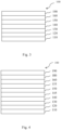
- FIG. 1 is a schematic sectional view of an organic electronic device 101, according to an exemplary embodiment of the present invention.
- the organic electronic device 101 includes a substrate (110), an anode layer (120), a semiconductor layer comprising a compound of formula (I) (130), a photoactive layer (PAL) (151) and a cathode layer (190).
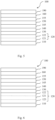
- FIG. 2 is a schematic sectional view of an organic light-emitting diode (OLED) 100, according to an exemplary embodiment of the present invention.
- the OLED 100 includes a substrate (110), an anode layer (120), a semiconductor layer comprising a compound of formula (I) (130), an emission layer (EML) (150) and a cathode layer (190).
- FIG. 3 is a schematic sectional view of an organic light-emitting diode (OLED) 100, according to an exemplary embodiment of the present invention.
- the OLED 100 includes a substrate (110), an anode layer (120), a semiconductor layer comprising a compound of formula (I) (130), a hole transport layer (HTL) (140), an emission layer (EML) (150), an electron transport layer (ETL) (160) and a cathode layer (190).
- FIG. 4 is a schematic sectional view of an organic light-emitting diode (OLED) 100, according to an exemplary embodiment of the present invention.
- the OLED 100 includes a substrate (110), an anode layer (120), a semiconductor layer comprising a compound of formula (I) (130), a hole transport layer (HTL) (140), an electron blocking layer (EBL) (145), an emission layer (EML) (150), a hole blocking layer (HBL) (155), an electron transport layer (ETL) (160), an optional electron injection layer (EIL) (180), and a cathode layer (190).
- FIG. 5 is a schematic sectional view of an organic light-emitting diode (OLED) 100, according to an exemplary embodiment of the present invention.
- the OLED 100 includes a substrate (110), an anode layer (120) that comprises a first anode sub-layer (121) and a second anode sub-layer (122), a semiconductor layer comprising compound of formula (I) (130), a hole transport layer (HTL) (140), an electron blocking layer (EBL) (145), an emission layer (EML) (150), a hole blocking layer (EBL) (155), an electron transport layer (ETL) (160) and a cathode layer (190).
- FIG. 6 is a schematic sectional view of an organic light-emitting diode (OLED) 100, according to an exemplary embodiment of the present invention.
- the OLED 100 includes a substrate (110), an anode layer (120) that comprises a first anode sub-layer (121), a second anode sub-layer (122) and a third anode sub-layer (123), a semiconductor layer comprising compound of formula (I) (130), a hole transport layer (HTL) (140), an electron blocking layer (EBL) (145), an emission layer (EML) (150), a hole blocking layer (EBL) (155), an electron transport layer (ETL) (160) and a cathode layer (190).
- the layers are disposed exactly in the order as mentioned before.
- an organic electronic device 101 of the present invention is for example started with a substrate (110) onto which an anode layer (120) is formed, on the anode layer (120), a semiconductor layer comprising compound of formula (I) (130), a photoactive layer (151) and a cathode electrode 190 are formed, exactly in that order or exactly the other way around.
- an OLED of the present invention is started with a substrate (110) onto which an anode layer (120) is formed, on the anode layer (120), a semiconductor layer comprising compound of formula (I) (130), optional a hole transport layer (140), optional an electron blocking layer (145), an emission layer (150), optional a hole blocking layer (155), optional an electron transport layer (160), optional an electron injection layer (180), and a cathode electrode 190 are formed, exactly in that order or exactly the other way around.
- a substrate (110) onto which an anode layer (120) is formed, on the anode layer (120), a semiconductor layer comprising compound of formula (I) (130), optional a hole transport layer (140), optional an electron blocking layer (145), an emission layer (150), optional a hole blocking layer (155), optional an electron transport layer (160), optional an electron injection layer (180), and a cathode electrode 190 are formed, exactly in that order or exactly the other way around.
- the semiconductor layer comprising a compound of formula (I) (130) can be a hole injection layer.
- a capping layer and/or a sealing layer may further be formed on the cathode electrodes 190, in order to seal the OLEDs 100.
- various other modifications may be applied thereto.
- the sublimation apparatus consist of an inner glass tube consisting of bulbs with a diameter of 3 cm which are placed inside a glass tube with a diameter of 3.5 cm.
- the sublimation apparatus is placed inside a tube oven (Creaphys DSU 05/2.1).
- the sublimation apparatus is evacuated via a membrane pump (Pfeiffer Vacuum MVP 055- 3C) and a turbo pump (Pfeiffer Vacuum THM071 YP).
- the pressure is measured between the sublimation apparatus and the turbo pump using a pressure gauge (Pfeiffer Vacuum PKR 251).
- the temperature is increased in increments of 10 to 30 K till the compound starts to be deposited in the harvesting zone of the sublimation apparatus.
- the temperature is further increased in increments of 10 to 30 K till a sublimation rate is achieved where the compound in the source is visibly depleted over 30 min to 1 hour and a substantial amount of compound has accumulated in the harvesting zone.
- the sublimation temperature also named T subl , is the temperature inside the sublimation apparatus at which the compound is deposited in the harvesting zone at a visible rate and is measured in degree Celsius.
- the rate onset temperature is determined by loading 100 mg compound into a VTE source.
- VTE source a point source for organic materials may be used as supplied by Kurt J. Lesker Company (www.lesker.com) or CreaPhys GmbH (http://www.creaphys.com).
- the VTE source is heated at a constant rate of 15 K/min at a pressure of less than 10 -5 mbar and the temperature inside the source measured with a thermocouple. Evaporation of the compound is detected with a QCM detector which detects deposition of the compound on the quartz crystal of the detector. The deposition rate on the quartz crystal is measured in ⁇ ngstrom per second. To determine the rate onset temperature, the deposition rate is plotted against the VTE source temperature. The rate onset is the temperature at which noticeable deposition on the QCM detector occurs. For accurate results, the VTE source is heated and cooled three time and only results from the second and third run are used to determine the rate onset temperature.
- the rate onset temperature may be in the range of 200 to 255 °C. If the rate onset temperature is below 200 °C the evaporation may be too rapid and therefore difficult to control. If the rate onset temperature is above 255 °C the evaporation rate may be too low which may result in low tact time and decomposition of the organic compound in VTE source may occur due to prolonged exposure to elevated temperatures.
- the rate onset temperature is an indirect measure of the volatility of a compound. The higher the rate onset temperature the lower is the volatility of a compound.
- a glass substrate with an anode layer comprising a first anode sub-layer of 120 nm Ag, a second anode sub-layer of 8 nm ITO and a third anode sub-layer of 10 nm ITO was cut to a size of 50 mm x 50 mm x 0.7 mm, ultrasonically washed with water for 60 minutes and then with isopropanol for 20 minutes.
- the liquid film was removed in a nitrogen stream, followed by plasma treatment to prepare the anode layer.
- the plasma treatment was performed in an atmosphere comprising 97.6 vol.-% nitrogen and 2.4 vol.-% oxygen at 75 W for 35 seconds.
- HIL hole injection layer
- Table 2 The composition of the hole injection layer can be seen in Table 2.
- inventive examples 1 to 3 a compound of formula (I) is used.
- Matrix compound HTM-1 has the following formula:
- the matrix compound was vacuum deposited on the HIL, to form an HTL having a thickness of 123 nm.
- the matrix compound in the HTL is selected the same as the matrix compound in the HIL.
- N-([1,1'-biphenyl]-4-yl)-9,9-diphenyl-N-(4-(triphenylsilyl)phenyl)-9H-fluoren-2-amine was vacuum deposited on the HTL, to form an electron blocking layer (EBL) having a thickness of 5 nm.
- EML blue-emitting first emission layer
- a hole blocking layer was formed with a thickness of 5 nm by depositing 2-(3'-(9,9-dimethyl-9H-fluoren-2-yl)-[1,1'-biphenyl]-3-yl)-4,6-diphenyl-1,3,5-triazine on the emission layer EML.
- the electron transporting layer having a thickness of 31 nm was formed on the hole blocking layer by depositing 50 wt.-% 4'-(4-(4-(4,6-diphenyl-1,3,5-triazin-2-yl)phenyl)naphthalen-1-yl)-[1,1'-biphenyl]-4-carbonitrile and 50 wt.-% of LiQ.
- Ag:Mg (90:10 vol.-%) was evaporated at a rate of 0.01 to 1 ⁇ /s at 10 -7 mbar to form a cathode layer with a thickness of 13 nm on the electron transporting layer.
- HTM-1 was deposited on the cathode layer to form a capping layer with a thickness of 75 nm.
- the OLED stack is protected from ambient conditions by encapsulation of the device with a glass slide. Thereby, a cavity is formed, which includes a getter material for further protection.
- the current efficiency is measured at 20°C.
- the current-voltage characteristic is determined using a Keithley 2635 source measure unit, by sourcing a voltage in V and measuring the current in mA flowing through the device under test. The voltage applied to the device is varied in steps of 0.1V in the range between 0V and 10V.
- the luminance-voltage characteristics and CIE coordinates are determined by measuring the luminance in cd/m 2 using an Instrument Systems CAS-140CT array spectrometer (calibrated by Deutsche Ak relie für sstelle (DAkkS)) for each of the voltage values.
- the cd/A efficiency at 10 mA/cm 2 is determined by interpolating the luminance-voltage and current-voltage characteristics, respectively.
- Lifetime LT of the device is measured at ambient conditions (20°C) and 30 mA/cm 2 , using a Keithley 2400 sourcemeter, and recorded in hours.
- the brightness of the device is measured using a calibrated photo diode.
- the lifetime LT is defined as the time till the brightness of the device is reduced to 97 % of its initial value.
- the sublimation temperature of comparative compounds 1 to 6 can either not be measured due to decomposition of the compound or the sublimation temperature is in the range of 95 to 120 °C.
- the rate onset temperature of comparative compounds 1 to 6 is the range of ⁇ 100 to 101 °C, see Table 1.
- Inventive compound 1 is a Cu(II) complex of formula (I). Inventive compound 1 differs from comparative compound 1 in the substituted heteroaryl substituent. The sublimation temperature is increased from 110 - 120 °C in comparative compound 1 to 186 °C in inventive compound 1. The rate onset temperature is also improved to 105 °C.
- Inventive compound 2 is a Fe(III) complex of formula (I).
- the sublimation temperature is 182 °C.
- the rate onset temperature is further improved to 128 °C.
- Inventive compound 3 is a Fe(III) complex of formula (I). It differs from inventive compound 2 in the substituents on the heteroaryl group. The sublimation temperature is further increased to 209 °C and the rate onset temperature is further improved to 146 °C.
- Inventive compound 4 is a Fe(III) complex of formula (I). It differs from inventive compound 2 and 3 in the substituted heteroaryl substituent. The sublimation temperature is still high at 182 °C and the rate onset temperature is high at 122 °C.
- Table 2 are shown OLED performance data for an increase in operating voltage over time U(100 h)-U(1h) and lifetime LT97 for inventive examples 1 to 3 and comparative examples 1 to 3.
- the semiconductor layer comprises 3 vol.-% metal complex La(fod) 3 .
- the increase in operating voltage over time is 1.07 V.
- the lifetime is 30 h.
- the semiconductor layer comprises 3 vol.-% G6.
- the increase in operating voltage over time is 0.2 V.
- the lifetime is 75 h.
- the semiconductor layer comprises 5 vol.-% metal complex La(fod) 3 .
- the increase in operating voltage over time is 0.85 V.
- the lifetime is 24 h.
- the semiconductor layer comprises 5 vol.-% G6.
- the increase in operating voltage over time is 0.3 V.
- the lifetime is 95 h.
- the semiconductor layer comprises 10 vol.-% metal complex La(fod) 3 .
- the increase in operating voltage over time is 0.89 V.
- the lifetime is 15 h.
- the semiconductor layer comprises 10 vol.-% G6.
- the increase in operating voltage over time is 0.09 V.
- the lifetime is 79 h.
- Table 1 Properties of comparative compounds 1 to 6 and compounds of formula (I) Example Compound Sublimation temperature Tsubl, [°C] Rate onset temperature T RO , [°C] Comparative compound 1 Cu(acac)2 110-120 ⁇ 100 Comparative compound 2 Cu(tfac)2 95-100 ⁇ 100 Comparative compound 3 Bi(tfac)3 decomposition ⁇ 100 Comparative compound 4 Bi(hfac)3 decomposition ⁇ 100 Comparative compound 5 Bi(fod)3 120 ⁇ 100 Comparative compound 6 La(fod) 3 101 Inventive compound 1 G21 186 105 Inventive compound 2 G6 182 128 Inventive compound 3 G5 209 146 Inventive compound 4 G13 182 122 Table 2: Performance of an electroluminescent device comprising a metal complex Metal complex Percentage metal complex in semiconductor layer [vol.-%] Matr
Landscapes
- Chemical & Material Sciences (AREA)
- Organic Chemistry (AREA)
- Inorganic Chemistry (AREA)
- Engineering & Computer Science (AREA)
- Materials Engineering (AREA)
- Electroluminescent Light Sources (AREA)
- Nitrogen And Oxygen Or Sulfur-Condensed Heterocyclic Ring Systems (AREA)
Priority Applications (1)
| Application Number | Priority Date | Filing Date | Title |
|---|---|---|---|
| EP24208778.1A EP4496458A3 (de) | 2020-07-27 | 2020-07-27 | Metallkomplexe von 3-(2,3,5-trifluor-6-(trifluormethyl)pyridin-4-yl)pentan-2,4-dion und ähnlichen liganden als halbleitermaterialien zur verwendung in elektronischen vorrichtungen |
Applications Claiming Priority (2)
| Application Number | Priority Date | Filing Date | Title |
|---|---|---|---|
| EP20187943.4A EP3945090B1 (de) | 2020-07-27 | 2020-07-27 | Metallkomplexe von 3-(2,3,5-trifluoro-6-(trifluoromethyl)pyridin-4-yl)pentan-2,4-dion und ähnlichen liganden als halbleitermaterialien zur verwendung in elektronischen vorrichtungen |
| EP24208778.1A EP4496458A3 (de) | 2020-07-27 | 2020-07-27 | Metallkomplexe von 3-(2,3,5-trifluor-6-(trifluormethyl)pyridin-4-yl)pentan-2,4-dion und ähnlichen liganden als halbleitermaterialien zur verwendung in elektronischen vorrichtungen |
Related Parent Applications (1)
| Application Number | Title | Priority Date | Filing Date |
|---|---|---|---|
| EP20187943.4A Division EP3945090B1 (de) | 2020-07-27 | 2020-07-27 | Metallkomplexe von 3-(2,3,5-trifluoro-6-(trifluoromethyl)pyridin-4-yl)pentan-2,4-dion und ähnlichen liganden als halbleitermaterialien zur verwendung in elektronischen vorrichtungen |
Publications (2)
| Publication Number | Publication Date |
|---|---|
| EP4496458A2 true EP4496458A2 (de) | 2025-01-22 |
| EP4496458A3 EP4496458A3 (de) | 2025-03-26 |
Family
ID=71833249
Family Applications (2)
| Application Number | Title | Priority Date | Filing Date |
|---|---|---|---|
| EP24208778.1A Pending EP4496458A3 (de) | 2020-07-27 | 2020-07-27 | Metallkomplexe von 3-(2,3,5-trifluor-6-(trifluormethyl)pyridin-4-yl)pentan-2,4-dion und ähnlichen liganden als halbleitermaterialien zur verwendung in elektronischen vorrichtungen |
| EP20187943.4A Active EP3945090B1 (de) | 2020-07-27 | 2020-07-27 | Metallkomplexe von 3-(2,3,5-trifluoro-6-(trifluoromethyl)pyridin-4-yl)pentan-2,4-dion und ähnlichen liganden als halbleitermaterialien zur verwendung in elektronischen vorrichtungen |
Family Applications After (1)
| Application Number | Title | Priority Date | Filing Date |
|---|---|---|---|
| EP20187943.4A Active EP3945090B1 (de) | 2020-07-27 | 2020-07-27 | Metallkomplexe von 3-(2,3,5-trifluoro-6-(trifluoromethyl)pyridin-4-yl)pentan-2,4-dion und ähnlichen liganden als halbleitermaterialien zur verwendung in elektronischen vorrichtungen |
Country Status (1)
| Country | Link |
|---|---|
| EP (2) | EP4496458A3 (de) |
Families Citing this family (6)
| Publication number | Priority date | Publication date | Assignee | Title |
|---|---|---|---|---|
| EP3859811B1 (de) | 2020-01-28 | 2025-03-19 | Novaled GmbH | Organische elektronische vorrichtung mit einer anodenschicht, einer kathodenschicht, mindestens einer emissionsschicht (eml) und mindestens einer lochinjektionsschicht (hil) |
| EP4152423A1 (de) * | 2021-09-20 | 2023-03-22 | Novaled GmbH | Organische elektronische vorrichtung mit mindestens einem metallkomplex der formel (i) |
| EP4152422A1 (de) * | 2021-09-20 | 2023-03-22 | Novaled GmbH | Organische elektronische vorrichtung mit einer anodenschicht, einer kathodenschicht, mindestens einer photoaktiven schicht und einer halbleiterschicht mit einem metallkomplex |
| EP4152425A1 (de) * | 2021-09-20 | 2023-03-22 | Novaled GmbH | Organische elektronische vorrichtung mit einem substrat, einer anodenschicht, einer kathodenschicht, mindestens einer ersten emissionsschicht und einer lochinjektionsschicht, wobei die lochinjektionsschicht einen metallkomplex der formel (i) und eine verbindung der formel (ii) umfasst, wobei die lochinjektionsschicht zwischen der anodenschicht und der mindestens einen ersten emissionsschicht angeordnet ist |
| CN119908192A (zh) | 2022-09-19 | 2025-04-29 | 诺瓦尔德股份有限公司 | 含有包含金属的化合物的包含阳极层、阴极层、第一发光层、空穴注入层和第一空穴传输层的电致发光器件 |
| EP4340581A1 (de) * | 2022-09-19 | 2024-03-20 | Novaled GmbH | Elektrolumineszente vorrichtung mit anodenschicht, kathodenschicht, lochinjektionsschicht und erster lochtransportschicht mit einer metallhaltigen verbindung. |
Citations (2)
| Publication number | Priority date | Publication date | Assignee | Title |
|---|---|---|---|---|
| US20150200374A1 (en) | 2010-03-31 | 2015-07-16 | Osram Opto Semiconductors Gmbh | Dopant for a Hole Conductor Layer for Organic Semiconductor Components, and Use Thereof |
| WO2016188604A1 (en) | 2015-05-22 | 2016-12-01 | Merck Patent Gmbh | Composition comprising an organic semiconductor and a metal complex |
Family Cites Families (10)
| Publication number | Priority date | Publication date | Assignee | Title |
|---|---|---|---|---|
| AR208071A1 (es) * | 1973-12-20 | 1976-11-30 | Cassella Ag | Procedimiento para la obtencion de derivados de 1-(alquil-piridil)-butan-1-ol y 1-(alquil-piridil)-but-2-en-1-ona de 1-fenoxi-3-amino-propan-2-ol y sus oxazolidinas y sales de adicion acidas |
| SE7415759L (de) * | 1973-12-20 | 1975-06-23 | Cassella Farbwerke Mainkur Ag | |
| US4980357A (en) * | 1990-03-01 | 1990-12-25 | Pfizer Inc. | Azolidinedione derivatives |
| US5158703A (en) * | 1991-04-03 | 1992-10-27 | Mitsui Toatsu Chemicals Inc. | Resin composition for ultraviolet luminescent screen |
| JP5713285B2 (ja) * | 2010-12-01 | 2015-05-07 | 独立行政法人物質・材料研究機構 | 金属錯体、色素増感酸化物半導体電極及び色素増感太陽能電池 |
| RU2470026C1 (ru) * | 2011-08-16 | 2012-12-20 | Учреждение Российской академии наук Физический институт им. П.Н. Лебедева РАН (ФИАН) | Люминесцирующие комплексные соединения редкоземельных элементов с пиразолсодержащими 1,3-дикетонами и способ их получения |
| RU2469041C1 (ru) * | 2011-08-16 | 2012-12-10 | Учреждение Российской академии наук Физический институт им. П.Н. Лебедева РАН (ФИАН) | Люминесцирующие комплексные соединения рзэ с пиразолсодержащими 1,3-дикетонами и способ их получения |
| RU2485162C1 (ru) * | 2011-12-09 | 2013-06-20 | Учреждение Российской академии наук Физический институт им. П.Н. Лебедева РАН (ФИАН) | Люминесцирующие анионные комплексные соединения редкоземельных элементов со фторированными пиразолсодержащими 1,3-дикетонами и способ их получения |
| WO2014104917A1 (en) * | 2012-12-28 | 2014-07-03 | Organic Lighting Solutions Ug | Rare earth metal ion complex, luminescent composite material, light emitting device, and use |
| US20230092935A1 (en) * | 2019-09-11 | 2023-03-23 | Credoxys GmbH | Cerium (iv) complexes and their use in organic electronics |
-
2020
- 2020-07-27 EP EP24208778.1A patent/EP4496458A3/de active Pending
- 2020-07-27 EP EP20187943.4A patent/EP3945090B1/de active Active
Patent Citations (2)
| Publication number | Priority date | Publication date | Assignee | Title |
|---|---|---|---|---|
| US20150200374A1 (en) | 2010-03-31 | 2015-07-16 | Osram Opto Semiconductors Gmbh | Dopant for a Hole Conductor Layer for Organic Semiconductor Components, and Use Thereof |
| WO2016188604A1 (en) | 2015-05-22 | 2016-12-01 | Merck Patent Gmbh | Composition comprising an organic semiconductor and a metal complex |
Non-Patent Citations (1)
| Title |
|---|
| no. 207739-72-8 |
Also Published As
| Publication number | Publication date |
|---|---|
| EP4496458A3 (de) | 2025-03-26 |
| EP3945090A1 (de) | 2022-02-02 |
| EP3945090B1 (de) | 2024-10-30 |
Similar Documents
| Publication | Publication Date | Title |
|---|---|---|
| EP3945090B1 (de) | Metallkomplexe von 3-(2,3,5-trifluoro-6-(trifluoromethyl)pyridin-4-yl)pentan-2,4-dion und ähnlichen liganden als halbleitermaterialien zur verwendung in elektronischen vorrichtungen | |
| EP3945125A1 (de) | Verbindung der formel (i), halbleitermaterial mit mindestens einer verbindung der formel (i), halbleiterschicht mit mindestens einer verbindung der formel (i) und elektronische vorrichtung mit mindestens einer verbindung der formel (i) | |
| US20230056322A1 (en) | Organic Electronic Device Comprising a Compound of Formula (I), Display Device Comprising the Organic Electronic Device as Well as Compounds of Formula (I) for Use in Organic Electronic Devices | |
| EP4199131A1 (de) | Ce(iv)-metallkomplex, organische elektronische vorrichtung mit einer anodenschicht, einer kathodenschicht und einer ladungserzeugungsschicht, wobei die ladungserzeugungsschicht eine p-ladungserzeugungsschicht mit einem ce(iv)-metallkomplex und einer n-ladungserzeugungsschicht umfasst | |
| US20230056395A1 (en) | Organic Electronic Device Comprising a Compound of Formula (I), Display Device Comprising the Organic Electronic Device as Well as Compounds of Formula (I) for Use in Organic Electronic Devices | |
| US20230006155A1 (en) | Organic Electronic Device Comprising a Compound of Formula (I), Display Device Comprising the Organic Electronic Device as Well as Compounds of Formula (I) for Use in Organic Electronic Devices | |
| US20230247896A1 (en) | Compound of Formula (I), a Semiconductor Material Comprising at Least One Compound of Formula (I), a Semiconductor Layer Comprising at Least One Compound of Formula (I) and an Electronic Device Comprising at Least One Compound of Formula (I) | |
| EP4106025A1 (de) | Organische elektronische vorrichtung mit einer verbindung der formel (1), anzeigevorrichtung mit der organischen elektronischen vorrichtung sowie verbindungen der formel (1) zur verwendung in organischen elektronischen vorrichtungen | |
| EP4321506A1 (de) | Metallkomplex, halbleiterschicht, die einen metallkomplex umfasst, und organische elektronische vorrichtung | |
| EP4151642B1 (de) | Verbindung, halbleiterschicht mit einer verbindung und organische elektronische vorrichtung | |
| US20230242562A1 (en) | Compound of Formula (I), a Semiconductor Material Comprising at Least One Compound of Formula (I), a Semiconductor Layer Comprising at Least One Compound of Formula (I) and an Electronic Device Comprising at Least One Compound of Formula (I) | |
| EP4516876B1 (de) | Verbindung der formel (i), organische elektronische vorrichtung mit einer verbindung der formel(1), anzeigevorrichtung | |
| EP4340582A1 (de) | Organische elektronische vorrichtung mit einer ladungserzeugungsschicht | |
| US20240397744A1 (en) | Organic Electronic Device Comprising at Least One Metal Complex of Formula (I) | |
| EP4382510B1 (de) | Verbindung der formel (i), organische elektronische vorrichtung mit einer verbindung der formel(1), anzeigevorrichtung | |
| US20240381760A1 (en) | Compound, Semiconductor Layer Comprising Compound and Organic Electronic Device | |
| EP4518635A1 (de) | Organische elektronische vorrichtung mit einer lochinjektionsschicht, welche verbindungen der formeln (i) und (iii) enthält | |
| US20240383935A1 (en) | Metal Complex, Semiconductor Layer Comprising a Metal Complex and Organic Electronic Device | |
| EP4434961A1 (de) | Verbindung der formel (i), organische elektronische vorrichtung mit einer verbindung der formel(i), anzeigevorrichtung | |
| EP4570808A1 (de) | Verbindung der formel (i), organische elektronische vorrichtung mit einer verbindung der formel (i), anzeigevorrichtung mit der organischen elektronischen vorrichtung | |
| EP4106026A1 (de) | Organische elektronische vorrichtung mit einem substrat, einer anodenschicht, einer kathodenschicht, mindestens einer ersten emissionsschicht und mindestens einer lochinjektionsschicht mit einem metallkomplex | |
| WO2024194321A1 (en) | Compound of formula (i); organic electronic device comprising a compound of formula (i); display device comprising the organic electronic device | |
| WO2024061807A1 (en) | Organic electronic device comprising a charge generation layer |
Legal Events
| Date | Code | Title | Description |
|---|---|---|---|
| PUAI | Public reference made under article 153(3) epc to a published international application that has entered the european phase |
Free format text: ORIGINAL CODE: 0009012 |
|
| STAA | Information on the status of an ep patent application or granted ep patent |
Free format text: STATUS: THE APPLICATION HAS BEEN PUBLISHED |
|
| AC | Divisional application: reference to earlier application |
Ref document number: 3945090 Country of ref document: EP Kind code of ref document: P |
|
| AK | Designated contracting states |
Kind code of ref document: A2 Designated state(s): AL AT BE BG CH CY CZ DE DK EE ES FI FR GB GR HR HU IE IS IT LI LT LU LV MC MK MT NL NO PL PT RO RS SE SI SK SM TR |
|
| REG | Reference to a national code |
Ref country code: DE Ref legal event code: R079 Free format text: PREVIOUS MAIN CLASS: H10K0085300000 Ipc: C07D0213610000 |
|
| PUAL | Search report despatched |
Free format text: ORIGINAL CODE: 0009013 |
|
| AK | Designated contracting states |
Kind code of ref document: A3 Designated state(s): AL AT BE BG CH CY CZ DE DK EE ES FI FR GB GR HR HU IE IS IT LI LT LU LV MC MK MT NL NO PL PT RO RS SE SI SK SM TR |
|
| RIC1 | Information provided on ipc code assigned before grant |
Ipc: H10K 85/30 20230101ALI20250218BHEP Ipc: C09B 57/10 20060101ALI20250218BHEP Ipc: C09B 57/00 20060101ALI20250218BHEP Ipc: C07F 15/03 20060101ALI20250218BHEP Ipc: C07F 15/02 20060101ALI20250218BHEP Ipc: C07F 15/00 20060101ALI20250218BHEP Ipc: H01M 14/00 20060101ALI20250218BHEP Ipc: C07D 209/86 20060101ALI20250218BHEP Ipc: C07D 213/61 20060101AFI20250218BHEP |
|
| STAA | Information on the status of an ep patent application or granted ep patent |
Free format text: STATUS: REQUEST FOR EXAMINATION WAS MADE |
|
| 17P | Request for examination filed |
Effective date: 20250926 |