EP4489084A2 - Optoelektronische vorrichtung mit leuchtdioden mit verbesserter lichtauskopplung und verfahren zu ihrer herstellung - Google Patents
Optoelektronische vorrichtung mit leuchtdioden mit verbesserter lichtauskopplung und verfahren zu ihrer herstellung Download PDFInfo
- Publication number
- EP4489084A2 EP4489084A2 EP24214655.3A EP24214655A EP4489084A2 EP 4489084 A2 EP4489084 A2 EP 4489084A2 EP 24214655 A EP24214655 A EP 24214655A EP 4489084 A2 EP4489084 A2 EP 4489084A2
- Authority
- EP
- European Patent Office
- Prior art keywords
- light
- layer
- optoelectronic device
- covering
- emitting diode
- Prior art date
- Legal status (The legal status is an assumption and is not a legal conclusion. Google has not performed a legal analysis and makes no representation as to the accuracy of the status listed.)
- Pending
Links
Images



Classifications
-
- H—ELECTRICITY
- H10—SEMICONDUCTOR DEVICES; ELECTRIC SOLID-STATE DEVICES NOT OTHERWISE PROVIDED FOR
- H10H—INORGANIC LIGHT-EMITTING SEMICONDUCTOR DEVICES HAVING POTENTIAL BARRIERS
- H10H20/00—Individual inorganic light-emitting semiconductor devices having potential barriers, e.g. light-emitting diodes [LED]
- H10H20/80—Constructional details
- H10H20/84—Coatings, e.g. passivation layers or antireflective coatings
-
- H—ELECTRICITY
- H10—SEMICONDUCTOR DEVICES; ELECTRIC SOLID-STATE DEVICES NOT OTHERWISE PROVIDED FOR
- H10H—INORGANIC LIGHT-EMITTING SEMICONDUCTOR DEVICES HAVING POTENTIAL BARRIERS
- H10H20/00—Individual inorganic light-emitting semiconductor devices having potential barriers, e.g. light-emitting diodes [LED]
- H10H20/80—Constructional details
- H10H20/81—Bodies
- H10H20/813—Bodies having a plurality of light-emitting regions, e.g. multi-junction LEDs or light-emitting devices having photoluminescent regions within the bodies
-
- H—ELECTRICITY
- H10—SEMICONDUCTOR DEVICES; ELECTRIC SOLID-STATE DEVICES NOT OTHERWISE PROVIDED FOR
- H10H—INORGANIC LIGHT-EMITTING SEMICONDUCTOR DEVICES HAVING POTENTIAL BARRIERS
- H10H20/00—Individual inorganic light-emitting semiconductor devices having potential barriers, e.g. light-emitting diodes [LED]
- H10H20/80—Constructional details
- H10H20/81—Bodies
- H10H20/817—Bodies characterised by the crystal structures or orientations, e.g. polycrystalline, amorphous or porous
- H10H20/818—Bodies characterised by the crystal structures or orientations, e.g. polycrystalline, amorphous or porous within the light-emitting regions
-
- H—ELECTRICITY
- H10—SEMICONDUCTOR DEVICES; ELECTRIC SOLID-STATE DEVICES NOT OTHERWISE PROVIDED FOR
- H10H—INORGANIC LIGHT-EMITTING SEMICONDUCTOR DEVICES HAVING POTENTIAL BARRIERS
- H10H20/00—Individual inorganic light-emitting semiconductor devices having potential barriers, e.g. light-emitting diodes [LED]
- H10H20/80—Constructional details
- H10H20/81—Bodies
- H10H20/819—Bodies characterised by their shape, e.g. curved or truncated substrates
-
- H—ELECTRICITY
- H10—SEMICONDUCTOR DEVICES; ELECTRIC SOLID-STATE DEVICES NOT OTHERWISE PROVIDED FOR
- H10H—INORGANIC LIGHT-EMITTING SEMICONDUCTOR DEVICES HAVING POTENTIAL BARRIERS
- H10H20/00—Individual inorganic light-emitting semiconductor devices having potential barriers, e.g. light-emitting diodes [LED]
- H10H20/80—Constructional details
- H10H20/83—Electrodes
- H10H20/831—Electrodes characterised by their shape
-
- H—ELECTRICITY
- H10—SEMICONDUCTOR DEVICES; ELECTRIC SOLID-STATE DEVICES NOT OTHERWISE PROVIDED FOR
- H10H—INORGANIC LIGHT-EMITTING SEMICONDUCTOR DEVICES HAVING POTENTIAL BARRIERS
- H10H20/00—Individual inorganic light-emitting semiconductor devices having potential barriers, e.g. light-emitting diodes [LED]
- H10H20/80—Constructional details
- H10H20/85—Packages
- H10H20/8504—Chip-scale type packages
-
- H—ELECTRICITY
- H10—SEMICONDUCTOR DEVICES; ELECTRIC SOLID-STATE DEVICES NOT OTHERWISE PROVIDED FOR
- H10H—INORGANIC LIGHT-EMITTING SEMICONDUCTOR DEVICES HAVING POTENTIAL BARRIERS
- H10H20/00—Individual inorganic light-emitting semiconductor devices having potential barriers, e.g. light-emitting diodes [LED]
- H10H20/80—Constructional details
- H10H20/85—Packages
- H10H20/851—Wavelength conversion means
- H10H20/8514—Wavelength conversion means characterised by their shape, e.g. plate or foil
-
- H—ELECTRICITY
- H10—SEMICONDUCTOR DEVICES; ELECTRIC SOLID-STATE DEVICES NOT OTHERWISE PROVIDED FOR
- H10H—INORGANIC LIGHT-EMITTING SEMICONDUCTOR DEVICES HAVING POTENTIAL BARRIERS
- H10H20/00—Individual inorganic light-emitting semiconductor devices having potential barriers, e.g. light-emitting diodes [LED]
- H10H20/80—Constructional details
- H10H20/85—Packages
- H10H20/852—Encapsulations
- H10H20/854—Encapsulations characterised by their material, e.g. epoxy or silicone resins
-
- H—ELECTRICITY
- H10—SEMICONDUCTOR DEVICES; ELECTRIC SOLID-STATE DEVICES NOT OTHERWISE PROVIDED FOR
- H10H—INORGANIC LIGHT-EMITTING SEMICONDUCTOR DEVICES HAVING POTENTIAL BARRIERS
- H10H20/00—Individual inorganic light-emitting semiconductor devices having potential barriers, e.g. light-emitting diodes [LED]
- H10H20/80—Constructional details
- H10H20/85—Packages
- H10H20/855—Optical field-shaping means, e.g. lenses
-
- H—ELECTRICITY
- H10—SEMICONDUCTOR DEVICES; ELECTRIC SOLID-STATE DEVICES NOT OTHERWISE PROVIDED FOR
- H10H—INORGANIC LIGHT-EMITTING SEMICONDUCTOR DEVICES HAVING POTENTIAL BARRIERS
- H10H20/00—Individual inorganic light-emitting semiconductor devices having potential barriers, e.g. light-emitting diodes [LED]
- H10H20/80—Constructional details
- H10H20/85—Packages
- H10H20/857—Interconnections, e.g. lead-frames, bond wires or solder balls
-
- H—ELECTRICITY
- H10—SEMICONDUCTOR DEVICES; ELECTRIC SOLID-STATE DEVICES NOT OTHERWISE PROVIDED FOR
- H10W—GENERIC PACKAGES, INTERCONNECTIONS, CONNECTORS OR OTHER CONSTRUCTIONAL DETAILS OF DEVICES COVERED BY CLASS H10
- H10W90/00—Package configurations
-
- H—ELECTRICITY
- H10—SEMICONDUCTOR DEVICES; ELECTRIC SOLID-STATE DEVICES NOT OTHERWISE PROVIDED FOR
- H10H—INORGANIC LIGHT-EMITTING SEMICONDUCTOR DEVICES HAVING POTENTIAL BARRIERS
- H10H20/00—Individual inorganic light-emitting semiconductor devices having potential barriers, e.g. light-emitting diodes [LED]
- H10H20/01—Manufacture or treatment
- H10H20/034—Manufacture or treatment of coatings
-
- H—ELECTRICITY
- H10—SEMICONDUCTOR DEVICES; ELECTRIC SOLID-STATE DEVICES NOT OTHERWISE PROVIDED FOR
- H10H—INORGANIC LIGHT-EMITTING SEMICONDUCTOR DEVICES HAVING POTENTIAL BARRIERS
- H10H20/00—Individual inorganic light-emitting semiconductor devices having potential barriers, e.g. light-emitting diodes [LED]
- H10H20/01—Manufacture or treatment
- H10H20/036—Manufacture or treatment of packages
- H10H20/0362—Manufacture or treatment of packages of encapsulations
-
- H—ELECTRICITY
- H10—SEMICONDUCTOR DEVICES; ELECTRIC SOLID-STATE DEVICES NOT OTHERWISE PROVIDED FOR
- H10H—INORGANIC LIGHT-EMITTING SEMICONDUCTOR DEVICES HAVING POTENTIAL BARRIERS
- H10H20/00—Individual inorganic light-emitting semiconductor devices having potential barriers, e.g. light-emitting diodes [LED]
- H10H20/80—Constructional details
- H10H20/81—Bodies
- H10H20/822—Materials of the light-emitting regions
- H10H20/824—Materials of the light-emitting regions comprising only Group III-V materials, e.g. GaP
- H10H20/825—Materials of the light-emitting regions comprising only Group III-V materials, e.g. GaP containing nitrogen, e.g. GaN
-
- H—ELECTRICITY
- H10—SEMICONDUCTOR DEVICES; ELECTRIC SOLID-STATE DEVICES NOT OTHERWISE PROVIDED FOR
- H10H—INORGANIC LIGHT-EMITTING SEMICONDUCTOR DEVICES HAVING POTENTIAL BARRIERS
- H10H20/00—Individual inorganic light-emitting semiconductor devices having potential barriers, e.g. light-emitting diodes [LED]
- H10H20/80—Constructional details
- H10H20/85—Packages
- H10H20/852—Encapsulations
- H10H20/853—Encapsulations characterised by their shape
Definitions
- the present description relates generally to optoelectronic devices based on semiconductor materials and their manufacturing methods.
- the present invention relates more particularly to optoelectronic devices comprising light-emitting diodes formed by three-dimensional elements, in particular semiconductor microwires or nanowires.
- Optoelectronic devices with light-emitting diodes are devices suitable for converting an electrical signal into electromagnetic radiation, and in particular devices dedicated to the emission of electromagnetic radiation, in particular light.
- Examples of three-dimensional elements suitable for producing light-emitting diodes are microwires or nanowires comprising a semiconductor material based on a compound predominantly comprising at least one element from group III and one element from group V (for example gallium nitride GaN), hereinafter called a III-V compound.
- the light extraction efficiency (LEE) of an optoelectronic device is generally defined as the ratio of the number of photons escaping from the optoelectronic device to the number of photons emitted by the diodes. electroluminescent. It is desirable that the extraction efficiency of an optoelectronic device be as high as possible.
- a disadvantage of existing optoelectronic devices is that a fraction of the photons emitted within each LED do not escape from the LED.
- an object of an embodiment is to overcome at least in part the drawbacks of the optoelectronic devices with light-emitting diodes, in particular with microwires or nanowires, described above and of their manufacturing methods.
- Another object of an embodiment is to increase the extraction efficiency of the optoelectronic device.
- Another object of an embodiment is to reduce the proportion of light that does not escape from each light emitting diode.
- Another object of an embodiment is to reduce the proportion of light emitted by one light emitting diode that is absorbed/trapped by neighboring light emitting diodes.
- the dielectric layer is interposed between the electrically conductive layer and the encapsulation block or the electrically conductive layer is interposed between the dielectric layer and the encapsulation block.
- each semiconductor element is made of a III-V compound.
- each semiconductor element comprises gallium nitride.
- the average diameter of each semiconductor element is between 200 nm and 2 ⁇ m and the average diameter of each encapsulation block is between 3 ⁇ m and 30 ⁇ m.
- the device further comprises, for at least one light-emitting diode, a photoluminescent layer covering the encapsulation block.
- the device comprises lenses covering the encapsulation blocks, the air gaps being present between the lenses.
- the device further comprises an angular filter covering the lenses.
- the angular filter comprises a layer at least partially opaque to visible light and crossed by openings.
- Another embodiment provides a method of manufacturing an optoelectronic device comprising a support comprising a face and light-emitting diodes resting on the face and comprising wire, conical, or frustoconical semiconductor elements.
- the method comprises forming, for each light-emitting diode or for each group of light-emitting diodes, an encapsulation block at least partially transparent to the radiation emitted by the light-emitting diodes and covering the light-emitting diode or the group of light-emitting diodes, the maximum thickness of the encapsulation block being between 1 ⁇ m and 30 ⁇ m, air gaps being present between the encapsulation blocks covering adjacent light-emitting diodes or adjacent groups of light-emitting diodes, and forming an electrically conductive layer covering the encapsulation blocks and in contact with each light-emitting diode, wherein the refractive index of the encapsulation block covering at least one of the light-emitting diodes
- Another embodiment provides a method of manufacturing an optoelectronic device comprising a support comprising a face and light-emitting diodes resting on the face and comprising wire, conical, or frustoconical semiconductor elements, the method comprising forming, for each light-emitting diode or for each group of light-emitting diodes, an encapsulation block at least partially transparent to the radiation emitted by the light-emitting diodes and covering the light-emitting diode or the group of light-emitting diodes, the maximum thickness of the encapsulation block being between 1 ⁇ m and 30 ⁇ m, air gaps being present between the encapsulation blocks covering adjacent light-emitting diodes or adjacent groups of light-emitting diodes, and forming an electrically conductive layer covering the encapsulation blocks and in contact with each light-emitting diode.
- the optoelectronic device comprises, for at least one of the encapsulation blocks, a conformal dielectric layer covering the encapsulation block, and at least partially transparent to the radiation emitted by the light-emitting diodes, the refractive index of the encapsulation block being between 1.8 and 2.2, the thickness of the dielectric layer being between 200 nm and 5 ⁇ m, and the refractive index of the dielectric layer being between 1.3 and 1.6.
- the method comprises forming lenses covering the encapsulation blocks.
- the method comprises forming a single-piece structure comprising the lenses, each lens comprising a housing and comprising securing the single-piece structure to the support, the encapsulation blocks being inserted into the housings.
- the expressions "about”, “approximately”, “substantially”, and “of the order of” mean to within 10%, preferably to within 5%.
- the term “conductive layer” means an electrically conductive layer and the term “insulating layer” means an electrically insulating layer.
- the present description relates to optoelectronic devices with three-dimensional elements, for example wire, conical or truncated conical elements, in particular microwires or nanowires.
- microwire designates a three-dimensional structure of elongated shape in a preferred direction of which at least two dimensions, called minor dimensions, are between 5 nm and 2.5 ⁇ m, preferably between 50 nm and 2.5 ⁇ m, the third dimension, called major dimension, being at least equal to 1 time, preferably at least 5 times and even more preferably at least 10 times, the largest of the minor dimensions.
- the minor dimensions may be less than or equal to approximately 1.5 ⁇ m, preferably between 100 nm and 1.5 ⁇ m, more preferably between 100 nm and 800 nm.
- the height of each microwire or nanowire may be greater than or equal to 500 nm, preferably between 1 ⁇ m and 50 ⁇ m.
- the term “wire” is used to mean “microwire or nanowire”.
- the mean line of the wire which passes through the barycenters of the cross sections, in planes perpendicular to the preferred direction of the wire, is substantially rectilinear and is subsequently called the "axis" of the wire.
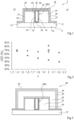
- FIG. 1 is a partial and schematic sectional view of an embodiment of an optoelectronic device 5 with light-emitting diodes, only one light-emitting diode being shown.
- the insulating layer 32 is not present. According to another embodiment, the insulating layer 32 is interposed between the conductive layer 30 and the encapsulation block 25.
- the LEDs are connected in parallel and form a set of LEDs.
- the electrodes 24 and 30 may be arranged to connect the LEDs differently.
- the insulating layer 32 is in contact with air 34.
- the front face 36 of the optoelectronic device 5 is the face seen by an observer and includes in particular the air-exposed faces 34 of the encapsulation blocks 25, when the layer 32 is not present, or the air-exposed faces 34 of the layer 32 when the layer 32 is present.
- an air gap 37 is interposed between each pair of adjacent light-emitting diodes.
- the material composing the encapsulation block 25 has an optical refractive index, also called refractive index, for the wavelengths of the radiation emitted by the light-emitting diodes LED, strictly lower than the refractive index of the material composing the wire 16 and strictly higher than the refractive index of the material composing the insulating layer 32.
- the optical refractive index is a dimensionless number that characterizes the optical properties of a medium, in particular absorption and diffusion.
- the refractive index is equal to the real part of the complex optical index.
- the refractive index can be determined, for example, by ellipsometry.
- the material making up the insulating layer 32 has an optical refractive index strictly lower than the refractive index of the material making up the encapsulation block 25 and strictly higher than the refractive index of air.
- the support 10 may correspond to a single-piece structure or comprise a base covered with a conductive layer.
- the upper face 12 is electrically conductive and is for example metallic, for example made of aluminum, silver, copper or zinc.
- the support 10 may comprise different insulated conductive regions electrically between them. This makes it possible to address the different light-emitting diodes independently.
- the face 12 may be reflective.
- the support 10 may then have a specular reflection.
- the support 10 may then have a Lambertian reflection. To obtain a surface having a Lambertian reflection, one possibility is to create irregularities on a conductive surface.
- a texturing of the surface of the base may be carried out before the deposition of the metal layer so that the face 12 of the metal layer, once deposited, has reliefs.
- the wires 16 are, at least in part, formed from at least one semiconductor material.
- the wires 16 may be, at least in part, formed from semiconductor materials comprising predominantly a III-V compound, for example a III-N compound.
- group III elements include gallium (Ga), indium (In) or aluminum (Al).
- III-N compounds are GaN, AlN, InN, InGaN, AlGaN or AlInGaN.
- Other group V elements may also be used, for example, phosphorus or arsenic.
- the elements in the III-V compound may be combined with different mole fractions.
- the wires 16 may include a dopant.
- the dopant may be selected from the group comprising a group II P-type dopant, e.g., magnesium (Mg), zinc (Zn), cadmium (Cd) or mercury (Hg), a group IV P-type dopant, e.g., carbon (C) or a group IV N-type dopant, e.g., silicon (Si), germanium (Ge), selenium (Se), sulfur (S), terbium (Tb) or tin (Sn).
- a group II P-type dopant e.g., magnesium (Mg), zinc (Zn), cadmium (Cd) or mercury (Hg
- a group IV P-type dopant e.g., carbon (C) or a group IV N-type dopant, e.g., silicon (Si), germanium (Ge), selenium (Se), sulfur (S), terbium (Tb) or tin (Sn).
- the cross section of the wires 16 may have different shapes, such as, for example, an oval, circular or polygonal shape, in particular triangular, rectangular, square or hexagonal.
- the height of each wire 16 may be between 250 nm and 50 ⁇ m.
- Each wire 16 may have a semiconductor structure elongated along an axis substantially perpendicular to the face 12.
- Each wire 16 may have a generally cylindrical shape.
- the axes of two adjacent wires 16 may be 0.5 ⁇ m to 10 ⁇ m apart and preferably 1.5 ⁇ m to 6 ⁇ m apart.
- the wires 16 can be regularly distributed, in particular according to a hexagonal or square network.
- the active layer is the layer from which the majority of the radiation provided by the light-emitting diode LED is emitted.
- the active layer may include confinement means, such as a single quantum well or multiple quantum wells.
- confinement means such as a single quantum well or multiple quantum wells.
- it is made up of alternating layers of GaN and of InGaN having respective thicknesses of 5 to 20 nm (e.g. 8 nm) and 1 to 10 nm (e.g. 2.5 nm).
- the GaN layers may be doped, for example N or P type.
- the active layer may comprise a single layer of InGaN, for example of thickness greater than 10 nm.
- the intermediate layer for example P-type doped, may correspond to a semiconductor layer or a stack of semiconductor layers and allows the formation of a PN or PIN junction, the active layer being comprised between the P-type intermediate layer and the N-type wire 16 of the PN or PIN junction.
- the connecting layer may correspond to a semiconductor layer or a stack of semiconductor layers and allows the formation of an ohmic contact between the intermediate layer and the electrode 24.
- the connecting layer may be very heavily doped of the type opposite to the wire 16, to the point of degenerating the semiconductor layer(s), for example P-type doped at a concentration greater than or equal to 10 20 atoms/cm 3 .
- the stack of semiconductor layers may comprise an electron blocking layer formed of a ternary alloy, for example aluminium gallium nitride (AlGaN) or aluminium indium nitride (AlInN) in contact with the active layer and the intermediate layer, to ensure a good distribution of the electric carriers in the active layer.
- AlGaN aluminium gallium nitride
- AlInN aluminium indium nitride
- Each electrode 24, 30 is adapted to polarize the active layer of the light-emitting diode LED and to allow the electromagnetic radiation emitted by the light-emitting diode LED to pass through.
- the material forming each electrode 24, 30 may be a transparent and conductive material such as indium-tin oxide (or ITO, English acronym for Indium Tin Oxide), pure zinc oxide, zinc oxide aluminum-doped gallium-doped zinc oxide, graphene, or silver nanowires.
- ITO Indium Tin Oxide
- each electrode layer 24, 30 has a thickness of between 5 nm and 200 nm, preferably between 30 nm and 100 nm.
- Each insulating layer 14, 28 and 32 may be made of a dielectric material, for example silicon oxide (SiO 2 ), silicon nitride (Si x N y , where x is approximately equal to 3 and y is approximately equal to 4, for example Si 3 N 4 ), silicon oxynitride (in particular of general formula SiO x N y , for example Si 2 ON 2 ), aluminum oxide (Al 2 O 3 ), hafnium oxide (HfO 2 ) or diamond.
- the thickness of each insulating layer 14 and 28 is between 5 nm and 500 nm, for example equal to approximately 30 nm.
- the layer 32 may, in addition, be made of an organic material, for example an organic polymer, or of an inorganic material, for example silicone.
- the thickness of the insulating layer 32, when present, is between 200 nm and 5 ⁇ m, for example equal to approximately 1 ⁇ m.
- the encapsulation block 25 may be made of an organic material or an inorganic material at least partially transparent to the radiation emitted by the light-emitting diode LED.
- the maximum thickness of the encapsulation block 25, measured perpendicular to the face 12, is preferably between 1 ⁇ m and 30 ⁇ m.
- the width of the encapsulation block 25 may correspond to the diameter of the circle circumscribed to the encapsulation block in top view. According to one embodiment, the width of the encapsulation block 25 is between 3 ⁇ m and 30 ⁇ m.
- the upper face 26 is flat and parallel to the face 12.
- the side wall 18 is perpendicular to the face 12. As a variant, the side wall 18 may be inclined relative to the face 12.
- the encapsulation block 25 may be made of an at least partially transparent organic material.
- the encapsulation block 25 may comprise a matrix of an at least partially transparent inorganic or organic material in which particles of a dielectric material are optionally distributed.
- the refractive index of the dielectric material making up the particles is strictly greater than the refractive index of the material making up the matrix.
- the encapsulation block 25 comprises a silicone matrix, also called polysiloxane, or a matrix made of an epoxy polymer and further comprises particles of a dielectric material distributed in the matrix.
- the particles are made of any type of material allowing the production of particles of relatively spherical nanometric dimensions and having a suitable refractive index.
- the particles may be made of titanium oxide (TiO 2 ), zirconium oxide (ZrO 2 ), zinc sulfide (ZnS), lead sulfide (PbS) or amorphous silicon (Si).
- the average diameter of a particle is the diameter of the sphere of the same volume.
- the average diameter of the particles of the dielectric material is between 2 nm and 250 nm.
- the volume concentration of the particles relative to the total weight of the encapsulation layer 34 is between 1% and 50%.
- the encapsulation block 25 may be made of one of the materials described above for the insulating layers 14, 28 and 32.
- the encapsulation block When layer 32 is not present, the encapsulation block has a refractive index of between 1.3 and 1.6. When layer 32 is present, the encapsulation block 25 has a refractive index of between 1.8 and 2.2 and the insulating layer 32 has a refractive index of between 1.3 and 1.6.
- the optoelectronic device advantageously makes it possible to increase the overall extraction efficiency of the optoelectronic device 5, i.e. escaping from the optoelectronic device 5 via the front face 36.
- the light To be perceived by an observer looking at the optoelectronic device 5, the light must leave the encapsulation blocks 25 via the front face 36.
- a surface treatment, called texturing can be applied to the front face 36 so as to form reliefs on the face 36.
- the encapsulation block 25, covered by the electrode 30, had an external diameter of 5 ⁇ m, the support 10 being made of aluminum, the electrode 24 was made of TCO, the electrode 30 was made of TCO, the wire 16 and the shell 22 were made of GaN, had a height of 5 ⁇ m and an external diameter of 1.25 ⁇ m.
- the layer 32 When the layer 32 is present, its refractive index is taken equal to 1.45.
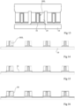
- FIG 2 represents curves of the evolution of the light extraction efficiency LEE of the optoelectronic device 5 of the figure 1 as a function of the refractive index n of the encapsulation block 25.
- the simulations indicated by diamonds were obtained in the absence of the layer 32, considering that the aluminum support 10 forms a mirror with a specular reflection.
- the simulations indicated by circles were obtained in the absence of the layer 32, considering that the support 10 has a Lambertian reflection.
- the simulation indicated by the square was obtained in the presence of the layer 32, considering that the aluminum support 10 forms a mirror with a specular reflection.
- the simulation indicated by the triangle was obtained in the presence of layer 32, considering that support 10 exhibits a Lambertian reflection.
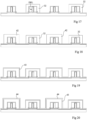
- FIG 3 is a partial and schematic sectional view of another embodiment of an optoelectronic device 40 with microwires or nanowires.
- the optoelectronic device 40 comprises all of the elements of the optoelectronic device 5 shown in figure 1 and further comprises, at least for some light-emitting diodes LED, a photoluminescent layer 42 covering the encapsulation block 25.
- the photoluminescent layer 42 may further play the role of the layer 32 described above.
- the refractive index range of the photoluminescent layer 42 is then that described above for the layer 32.
- the optoelectronic device 40 may further comprise a transparent layer 43 covering the photoluminescent layer 42 and a filter 44 covering the layer 43 configured to block the transmission of radiation in a given wavelength range.
- the filter 44 may correspond to a colored layer or to a stack of layers of different refractive indices forming a Bragg filter.
- the photoluminescent layer 42 may be a conformal layer.
- the filters 44 make it possible to adjust the wavelength range of the radiation escaping from the photoluminescent layer 42.
- the layer 43 has a refractive index as close as possible to 1, preferably lower than the refractive index of the layer 42, preferably lower than 1.5, so as to reduce, or even eliminate, the reflections on the filter 44 of the rays escaping from the photoluminescent layer 42.
- the layer 43 is for example made of MgF 2 , of a polymer, for example an acrylate, or corresponds to an air film.
- the photoluminescent layer 42 may comprise suitable phosphors, when excited by light emitted by the associated light emitting diode LED, to emit light at a wavelength different from the wavelength of the light emitted by the associated light emitting diode LED.
- the thickness of the photoluminescent 42 may be between 4 ⁇ m and 40 ⁇ m.
- the photoluminescent layer 42 comprises particles of at least one photoluminescent material.
- An example of a photoluminescent material is trivalent cerium ion activated yttrium aluminum garnet (YAG), also referred to as YAG:Ce or YAG:Ce3+.
- YAG trivalent cerium ion activated yttrium aluminum garnet
- the average particle size of conventional photoluminescent materials is typically greater than 5 ⁇ m.
- each photoluminescent layer 42 comprises a matrix in which are dispersed nanometric-sized monocrystalline particles of a semiconductor material, also called semiconductor nanocrystals or nanoluminophore particles hereinafter.
- the internal quantum efficiency QYint of a photoluminescent material is equal to the ratio between the number of photons emitted and the number of photons absorbed by the photoluminescent substance.
- the internal quantum efficiency QYint of the semiconductor nanocrystals is greater than 5%, preferably greater than 10%, more preferably greater than 20%.
- the average size of the nanocrystals is in the range of 0.5 nm and 1000 nm, preferably from 0.5 nm to 500 nm, even more preferably from 1 nm to 100 nm, in particular from 2 nm to 30 nm.
- the photoconversion properties of the semiconductor nanocrystals depend essentially on quantum confinement phenomena.
- the semiconductor nanocrystals then correspond to boxes quantum (in the case of confinement in three dimensions) or quantum wells (in the case of confinement in two dimensions).
- the semiconductor material of the semiconductor nanocrystals is selected from the group comprising cadmium selenide (CdSe), indium phosphide (InP), cadmium sulfide (CdS), zinc sulfide (ZnS), zinc selenide (ZnSe), cadmium telluride (CdTe), zinc telluride (ZnTe), cadmium oxide (CdO), zinc cadmium oxide (ZnCdO), zinc cadmium sulfide (CdZnS), zinc cadmium selenide (CdZnSe), silver indium sulfide (AgInS 2 ), perovskites of the PbScX 3 type, where X is a halogen atom, in particular iodine (I), bromine (Br) or chlorine (Cl), and a mixture of at least two of these compounds.
- X is a halogen atom, in particular iodine (I
- the semiconductor material of the semiconductor nanocrystals is chosen from the materials cited in the publication in the name of Le Blevenec et al. by Physica Status Solidi (RRL) - Rapid Research Letters Volume 8, No. 4, pages 349-352, April 2014 .
- the dimensions of the semiconductor nanocrystals are chosen according to the desired wavelength of the radiation emitted by the semiconductor nanocrystals.
- CdSe nanocrystals whose average size is of the order of 3.6 nm are suitable for converting blue light into red light and CdSe nanocrystals whose average size is of the order of 1.3 nm are suitable for converting blue light into green light.
- the composition of the semiconductor nanocrystals is chosen according to the desired wavelength of the radiation emitted by the semiconductor nanocrystals.
- the matrix is made of a material at least partly transparent to the radiation emitted by the light-emitting diode LED and to the radiation emitted by the photoluminescent particles.
- the matrix is, for example, made of silica.
- the matrix is, for example, made of any polymer at least partly transparent, in particular silicone, epoxy or polyacetic acid (PLA).
- PPA polyacetic acid
- the matrix can be made of an at least partly transparent polymer used with three-dimensional printers, such as PLA.
- the matrix contains from 2% to 90%, preferably from 10% to 60%, by weight of nanocrystals, for example approximately 30% by weight of nanocrystals.
- the matrix can further contain diffusing particles, in particular TiO 2 particles, having for example a diameter of between 100 nm and 300 nm.
- FIG 4 represents curves of evolution of the optical efficiency of POE pixel of the optoelectronic device 40 of the figure 3 as a function of the thickness E42 of the photoluminescent layer 42.
- the pixel optical efficiency corresponds to the ratio between the optical power emitted towards free space (including conversion losses) and the optical power generated by the light-emitting diode.
- the simulations indicated by diamonds were obtained when the support 10 corresponds to an opaque and matt material between the light-emitting diodes, i.e. a material having a substantially Lambertian reflection.
- the simulations indicated by circles were obtained when the support 10 corresponds to a mirror between the diodes electroluminescent, that is to say having a substantially specular reflection.
- FIG 5 is a partial and schematic sectional view of another embodiment of an optoelectronic device 50 with microwires or nanowires.
- the optoelectronic device 50 comprises all of the elements of the optoelectronic device 40 shown in figure 3 except that, for each light-emitting diode LED, the device 50 further comprises a conductive pad 52 interposed between the light-emitting diode LED and the support 10, that the insulating layer 14 covers the lateral edges of the conductive pad 52, that the shell 22 and the electrode 30 do not cover the lower end wall 19 of the wire 16 but the upper end wall 20 of the wire 16, that the insulating layer 28 is interposed between the conductive pad 52 and the electrode layer 30, and that the protuberance 29 connects the wire 16 to the conductive pad 52.
- FIG 6 is a partial and schematic sectional view of another embodiment of a microwire or nanowire optoelectronic device 55.
- the device optoelectronic device 55 comprises all the elements of the optoelectronic device 5 shown in figure 1 and further comprises, for each light-emitting diode LED, a lens 56 which completely covers the encapsulation block 25.
- the lens 56 covers the upper face of the encapsulation block 25 and the side wall of the encapsulation block 25.
- the lens 56 comprises an outer face 58 in contact with the air 34 which has at least in part substantially the shape of a parabola in a section plane containing the axis of the wire 16.
- the air gap 37 is present and interposed between two lenses 56 covering the light-emitting diodes LED of a pair of adjacent light-emitting diodes.
- the lens 56 may be made of an organic or inorganic material, in particular the materials described above for forming the encapsulation block 25 and/or the matrix of the photoluminescent layer 42.
- the lens 56 makes it possible to improve the directivity of the light emitted by the optoelectronic device 55.
- the thickness Zmax of the lens 56 corresponds to the maximum distance between the electrode layer 30 and the face 58.
- the width Ymax of the lens 56 corresponds to the maximum distance of the lens 56 measured parallel to the face 12 of the support 10. According to one embodiment, the thickness Zmax is between 8 ⁇ m and 50 ⁇ m. According to one embodiment, the width Ymax is between 8 ⁇ m and 50 ⁇ m.
- the refractive index of the lens 56 is between 1.4 and 1.5.
- the support 10 is reflective for the radiation emitted by the light-emitting diode LED and the side wall of the lens 56, on a lower portion of the lens 56, is surrounded by a reflective layer for the radiation emitted by the light-emitting diode LED.
- Lens 56 was made of material with a refractive index equal to 1.45.
- the maximum width Ymax of lens 56 was equal to the maximum thickness Zmax of lens 56.
- FIG 7 represents curves C1, C2 and C3 of the evolution of the energy intensity I of the radiation emitted by the optoelectronic device 55 of the figure 6 in a given direction as a function of the inclination Angle of said direction with the upper face 12 of the support 10 when the lens 56 has a maximum thickness Zmax equal to respectively 6 ⁇ m, 12 ⁇ m and 18 ⁇ m.
- the energy intensity at low incidences that is to say for radiation escaping substantially orthogonally to the face 12 of the support 10 increases when the maximum thickness Zmax of the lens 56 increases.
- FIG 8 represents a curve of the evolution of the luminous power P emitted by the optoelectronic device 55 of the figure 6 in an emission cone, with an axis perpendicular to the face 12 of the support 10 and whose half-angle at the apex is 20°, depending on the maximum thickness Zmax of the lens 56.
- the simulations indicated by large solid black circles were obtained with a lens 56 whose external face 58 corresponds to a paraboloid.
- two simulations indicated by large hollow circles were obtained with pyramid-shaped lenses.
- the luminous power in the emission cone increases when the maximum thickness Zmax of the lens 56 increases.
- the line P1 represented by small hollow circles represents the luminous power P emitted, in the emission cone defined previously, in the absence of the lens 56 and the line P2 represented by small solid circles represents the luminous power P which would be emitted, in the emission cone defined previously, by a Lambertian emitter.
- FIG 9 is a partial and schematic sectional view of another embodiment of an optoelectronic device 60 with microwires or nanowires.
- the optoelectronic device 60 comprises all of the elements of the optoelectronic device 40 shown in figure 3 and further comprises the lens 56 of the optoelectronic device 55 shown in figure 6 .
- the lens 56 completely covers the encapsulation block 25, the photoluminescent layer 42 being interposed between the encapsulation block 25 and the lens 56.
- FIG 10 is a partial and schematic sectional view of another embodiment of an optoelectronic device 65 with microwires or nanowires.
- the optoelectronic device 65 comprises all of the elements of the optoelectronic device 55 shown in figure 6 , three light-emitting diodes LED being shown, and further comprises an angular filter 66 covering the light-emitting diodes LED.
- the angular filter 66 is configured to block rays emitted by the light-emitting diodes LED and rays of ambient light outside the optoelectronic device 65 whose incidence relative to a reference direction, for example a direction orthogonal to the face 12 of the support 10, is in a first range of incidences and to allow rays to pass whose direction is in at least a second incidence range distinct from the first incidence range.
- the angular filter 66 comprises a layer 68 opaque to visible light, preferably absorbing visible light, and comprising through openings 69.
- the through openings 69 can be formed vertically above the light-emitting diodes LED in the reference direction.
- each light emitting diode LED is covered with a lens 56 as shown in figure 10 .
- the angular filter 66 is held apart from the support 10 by spacers not shown, an air film 34 being present between the angular filter 66 and the lenses 56. Since a significant portion of the radiation escaping from the lenses 56 has a low incidence relative to the reference direction, most of this radiation passes through the angular filter 66 without being blocked. Conversely, most of the radiation due to ambient light is blocked by the angular filter 66. This makes it possible to reduce unwanted reflections of ambient light on reflective elements of the optoelectronic device 65, for example metal tracks. This also makes it possible to improve the contrast of the optoelectronic device 65.
- the lenses 56 may be formed by depositing a layer of the material composing the lenses on the light-emitting diodes and etching this layer or forming this layer to obtain the lenses 56.
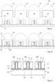
- FIGs 21 and 22 are partial and schematic sectional views of structures obtained at successive stages of an embodiment of a method of manufacturing an optoelectronic device corresponding to a variant of the optoelectronic device 60 shown in figure 9 .
- the lenses 56 are preformed separately from the structure comprising the light-emitting diodes.
- the lenses 56 form a single-piece structure 82, for example obtained by molding.
- Each lens 56 comprises a housing 84 intended to receive a light-emitting diode LED.
- the filters 44 can be formed in certain housings.
- the structure monobloc 82 is then fixed to the support 10 ( figure 22 ), for example by using a bonding material 86.
- the dimensions of the housings 84 are larger than the dimensions of the light-emitting diodes LED so that, when the single-piece structure 82 is fixed to the support 10, there remains an air gap between each lens 56 and the photoluminescent layer 42 which forms the layer 43 described above.
- the structure of the light emitting diode LED of the optoelectronic device 50 shown in figure 5 can be implemented with the optoelectronic device 5 shown in figure 1 , the optoelectronic device 55 shown in figure 6 , the optoelectronic device 60 shown in figure 9 and the optoelectronic device 65 shown in figure 10 .
- each encapsulation block 25 is shown covering a single light emitting diode LED, it is clear that each encapsulation block 25 may cover a group of light emitting diodes, for example from 2 to 100 light emitting diodes. The encapsulation block 25 may cover each light emitting diode in the group over the entire sidewall 18 of the light emitting diode.
Landscapes
- Led Device Packages (AREA)
- Led Devices (AREA)
Applications Claiming Priority (3)
| Application Number | Priority Date | Filing Date | Title |
|---|---|---|---|
| FR1871254A FR3087579B1 (fr) | 2018-10-22 | 2018-10-22 | Dispositif optoelectronique a diodes electroluminescentes a extraction de lumiere amelioree |
| PCT/EP2019/078320 WO2020083757A1 (fr) | 2018-10-22 | 2019-10-18 | Dispositif optoelectronique a diodes electroluminescentes a extraction de lumiere amelioree |
| EP19789681.4A EP3871255B1 (de) | 2018-10-22 | 2019-10-18 | Optoelektronische vorrichtung mit leuchtdioden mit verbesserter lichtextraktion und ein verfahren zu seiner herstellung |
Related Parent Applications (1)
| Application Number | Title | Priority Date | Filing Date |
|---|---|---|---|
| EP19789681.4A Division EP3871255B1 (de) | 2018-10-22 | 2019-10-18 | Optoelektronische vorrichtung mit leuchtdioden mit verbesserter lichtextraktion und ein verfahren zu seiner herstellung |
Publications (2)
| Publication Number | Publication Date |
|---|---|
| EP4489084A2 true EP4489084A2 (de) | 2025-01-08 |
| EP4489084A3 EP4489084A3 (de) | 2025-03-12 |
Family
ID=65763625
Family Applications (2)
| Application Number | Title | Priority Date | Filing Date |
|---|---|---|---|
| EP19789681.4A Active EP3871255B1 (de) | 2018-10-22 | 2019-10-18 | Optoelektronische vorrichtung mit leuchtdioden mit verbesserter lichtextraktion und ein verfahren zu seiner herstellung |
| EP24214655.3A Pending EP4489084A3 (de) | 2018-10-22 | 2019-10-18 | Optoelektronische vorrichtung mit leuchtdioden mit verbesserter lichtauskopplung und verfahren zu ihrer herstellung |
Family Applications Before (1)
| Application Number | Title | Priority Date | Filing Date |
|---|---|---|---|
| EP19789681.4A Active EP3871255B1 (de) | 2018-10-22 | 2019-10-18 | Optoelektronische vorrichtung mit leuchtdioden mit verbesserter lichtextraktion und ein verfahren zu seiner herstellung |
Country Status (8)
| Country | Link |
|---|---|
| US (2) | US12027505B2 (de) |
| EP (2) | EP3871255B1 (de) |
| JP (2) | JP7449584B2 (de) |
| KR (2) | KR20240161848A (de) |
| CN (2) | CN112956021B (de) |
| FR (1) | FR3087579B1 (de) |
| TW (2) | TW202508097A (de) |
| WO (1) | WO2020083757A1 (de) |
Families Citing this family (2)
| Publication number | Priority date | Publication date | Assignee | Title |
|---|---|---|---|---|
| CN111430340B (zh) * | 2020-03-31 | 2022-03-18 | 佛山市国星光电股份有限公司 | 一种led显示单元组及显示面板 |
| US11828944B1 (en) * | 2020-04-09 | 2023-11-28 | Apple Inc. | Head-mounted device with optical module illumination systems |
Citations (1)
| Publication number | Priority date | Publication date | Assignee | Title |
|---|---|---|---|---|
| US9537044B2 (en) | 2012-10-26 | 2017-01-03 | Aledia | Optoelectric device and method for manufacturing the same |
Family Cites Families (22)
| Publication number | Priority date | Publication date | Assignee | Title |
|---|---|---|---|---|
| JP2004235337A (ja) * | 2003-01-29 | 2004-08-19 | Toyoda Gosei Co Ltd | 発光ダイオード |
| US20050280016A1 (en) * | 2004-06-17 | 2005-12-22 | Mok Thye L | PCB-based surface mount LED device with silicone-based encapsulation structure |
| JP4923465B2 (ja) * | 2005-07-27 | 2012-04-25 | 凸版印刷株式会社 | 極端紫外線露光用マスクブランク、極端紫外線露光用マスク及びその製造方法並びにパターン転写方法 |
| US20070023765A1 (en) * | 2005-07-29 | 2007-02-01 | Thomas Alan C | Acicular ITO for LED array |
| DE102007025092A1 (de) * | 2007-05-30 | 2008-12-04 | Osram Opto Semiconductors Gmbh | Lumineszenzdiodenchip |
| TWI380481B (en) * | 2009-01-13 | 2012-12-21 | Huga Optotech Inc | Light-emitting diode with high light-emitting efficiency |
| US8168998B2 (en) * | 2009-06-09 | 2012-05-01 | Koninklijke Philips Electronics N.V. | LED with remote phosphor layer and reflective submount |
| CN102593113B (zh) * | 2011-01-10 | 2015-04-01 | 展晶科技(深圳)有限公司 | 发光二极管封装结构 |
| US8653542B2 (en) * | 2011-01-13 | 2014-02-18 | Tsmc Solid State Lighting Ltd. | Micro-interconnects for light-emitting diodes |
| DE102011116752B4 (de) * | 2011-10-24 | 2025-07-24 | OSRAM Opto Semiconductors Gesellschaft mit beschränkter Haftung | Optoelektronisches Halbleiterbauteil und Streumittel |
| FR2997558B1 (fr) * | 2012-10-26 | 2015-12-18 | Aledia | Dispositif opto-electrique et son procede de fabrication |
| DE112013005849T5 (de) * | 2012-12-06 | 2015-08-20 | Seoul Viosys Co., Ltd. | Lichtemittierende Diode und Anwendung dafür |
| US9111464B2 (en) * | 2013-06-18 | 2015-08-18 | LuxVue Technology Corporation | LED display with wavelength conversion layer |
| FR3011383B1 (fr) * | 2013-09-30 | 2017-05-26 | Commissariat Energie Atomique | Procede de fabrication de dispositifs optoelectroniques a diodes electroluminescentes |
| US9190563B2 (en) | 2013-11-25 | 2015-11-17 | Samsung Electronics Co., Ltd. | Nanostructure semiconductor light emitting device |
| FR3015772B1 (fr) * | 2013-12-19 | 2017-10-13 | Aledia | Dispositif optoelectronique a diodes electroluminescentes a extraction de lumiere amelioree |
| KR102285786B1 (ko) * | 2014-01-20 | 2021-08-04 | 삼성전자 주식회사 | 반도체 발광 소자 |
| KR102188494B1 (ko) * | 2014-07-21 | 2020-12-09 | 삼성전자주식회사 | 반도체 발광소자, 반도체 발광소자 제조방법 및 반도체 발광소자 패키지 제조방법 |
| CN106716650B (zh) | 2014-10-01 | 2018-10-09 | 日本碍子株式会社 | 发光元件及发光元件的制造方法 |
| KR102252994B1 (ko) * | 2014-12-18 | 2021-05-20 | 삼성전자주식회사 | 발광소자 패키지 및 발광소자 패키지용 파장 변환 필름 |
| JP2017108020A (ja) * | 2015-12-10 | 2017-06-15 | パナソニックIpマネジメント株式会社 | レンズユニット、ledモジュールおよびそれを用いた照明器具 |
| FR3053530B1 (fr) * | 2016-06-30 | 2018-07-27 | Aledia | Dispositif optoelectronique a pixels a contraste et luminance ameliores |
-
2018
- 2018-10-22 FR FR1871254A patent/FR3087579B1/fr active Active
-
2019
- 2019-10-18 US US17/287,087 patent/US12027505B2/en active Active
- 2019-10-18 JP JP2021522014A patent/JP7449584B2/ja active Active
- 2019-10-18 EP EP19789681.4A patent/EP3871255B1/de active Active
- 2019-10-18 KR KR1020247036951A patent/KR20240161848A/ko active Pending
- 2019-10-18 KR KR1020217012776A patent/KR102728553B1/ko active Active
- 2019-10-18 CN CN201980069833.4A patent/CN112956021B/zh active Active
- 2019-10-18 CN CN202410642992.1A patent/CN118507621A/zh active Pending
- 2019-10-18 WO PCT/EP2019/078320 patent/WO2020083757A1/fr not_active Ceased
- 2019-10-18 EP EP24214655.3A patent/EP4489084A3/de active Pending
- 2019-10-21 TW TW113137504A patent/TW202508097A/zh unknown
- 2019-10-21 TW TW108137858A patent/TWI861020B/zh active
-
2024
- 2024-02-26 JP JP2024026757A patent/JP7716130B2/ja active Active
- 2024-05-29 US US18/676,771 patent/US20240321843A1/en active Pending
Patent Citations (1)
| Publication number | Priority date | Publication date | Assignee | Title |
|---|---|---|---|---|
| US9537044B2 (en) | 2012-10-26 | 2017-01-03 | Aledia | Optoelectric device and method for manufacturing the same |
Non-Patent Citations (1)
| Title |
|---|
| LE BLEVENEC ET AL., PHYSICA STATUS SOLIDI (RRL) - RAPID RESEARCH LETTERS, vol. 8, no. 4, April 2014 (2014-04-01), pages 349 - 352 |
Also Published As
| Publication number | Publication date |
|---|---|
| US20210384175A1 (en) | 2021-12-09 |
| TW202032814A (zh) | 2020-09-01 |
| JP7716130B2 (ja) | 2025-07-31 |
| WO2020083757A1 (fr) | 2020-04-30 |
| KR20210070327A (ko) | 2021-06-14 |
| CN112956021B (zh) | 2024-06-04 |
| US12027505B2 (en) | 2024-07-02 |
| KR102728553B1 (ko) | 2024-11-11 |
| EP4489084A3 (de) | 2025-03-12 |
| JP2022505613A (ja) | 2022-01-14 |
| JP7449584B2 (ja) | 2024-03-14 |
| CN112956021A (zh) | 2021-06-11 |
| TWI861020B (zh) | 2024-11-11 |
| FR3087579A1 (fr) | 2020-04-24 |
| EP3871255A1 (de) | 2021-09-01 |
| EP3871255B1 (de) | 2024-12-04 |
| JP2024059832A (ja) | 2024-05-01 |
| US20240321843A1 (en) | 2024-09-26 |
| KR20240161848A (ko) | 2024-11-12 |
| FR3087579B1 (fr) | 2022-08-12 |
| CN118507621A (zh) | 2024-08-16 |
| TW202508097A (zh) | 2025-02-16 |
Similar Documents
| Publication | Publication Date | Title |
|---|---|---|
| EP3646392B1 (de) | Optoelektronische vorrichtung | |
| EP3373345B1 (de) | Optoelektronische vorrichtung mit leuchtdioden mit verbesserter lichtextraktion | |
| EP3948949B1 (de) | Verfahren zur herstellung eines emissiven dreidimensionalen led-bildschirms und resultierender bildschirm | |
| WO2021130136A1 (fr) | Dispositif pour traitement par laser et procédé de traitement au laser | |
| US20240321843A1 (en) | Optoelectronic device comprising light-emitting diodes with improved light extraction | |
| FR3118289A1 (fr) | Dispositif optoélectronique à diodes électroluminescentes tridimensionnelles de type axial | |
| FR3087580A1 (fr) | Procede de realisation d’un dispositif optoelectronique comprenant des diodes electroluminescentes homogenes en dimensions | |
| FR3082657A1 (fr) | Procede de fabrication d’un dispositif optoelectronique a parois de confinement lumineux auto alignes | |
| EP3113235B1 (de) | Elektrolumineszenzvorrichtung | |
| WO2015155437A1 (fr) | Dispositif optoelectronique a diodes electroluminescentes et a diagramme d'emission ameliore | |
| FR3046292A1 (fr) | Circuit electronique comprenant des tranchees d'isolation electrique | |
| EP4264681A1 (de) | Optoelektronische vorrichtung mit dreidimensionalen leuchtdioden vom axialtyp | |
| EP3903354B1 (de) | Optoelektronische vorrichtung mit einer mikrometrischen oder nanometrischen lichtemittierenden diode, die mit einer optischen linse überzogen ist | |
| FR3166031A1 (fr) | Dispositif optoélectronique émissif à taux de conversion de couleur amélioré et procédé de fabrication | |
| FR3082662A1 (fr) | Procédé de fabrication d’un dispositif optoélectronique à parois de confinement lumineux auto alignés |
Legal Events
| Date | Code | Title | Description |
|---|---|---|---|
| PUAI | Public reference made under article 153(3) epc to a published international application that has entered the european phase |
Free format text: ORIGINAL CODE: 0009012 |
|
| STAA | Information on the status of an ep patent application or granted ep patent |
Free format text: STATUS: REQUEST FOR EXAMINATION WAS MADE |
|
| 17P | Request for examination filed |
Effective date: 20241121 |
|
| AC | Divisional application: reference to earlier application |
Ref document number: 3871255 Country of ref document: EP Kind code of ref document: P |
|
| AK | Designated contracting states |
Kind code of ref document: A2 Designated state(s): AL AT BE BG CH CY CZ DE DK EE ES FI FR GB GR HR HU IE IS IT LI LT LU LV MC MK MT NL NO PL PT RO RS SE SI SK SM TR |
|
| REG | Reference to a national code |
Ref country code: DE Ref legal event code: R079 Free format text: PREVIOUS MAIN CLASS: H01L0033320000 Ipc: H10H0020840000 |
|
| PUAL | Search report despatched |
Free format text: ORIGINAL CODE: 0009013 |
|
| AK | Designated contracting states |
Kind code of ref document: A3 Designated state(s): AL AT BE BG CH CY CZ DE DK EE ES FI FR GB GR HR HU IE IS IT LI LT LU LV MC MK MT NL NO PL PT RO RS SE SI SK SM TR |
|
| RIC1 | Information provided on ipc code assigned before grant |
Ipc: H10H 20/854 20250101ALI20250205BHEP Ipc: H10H 20/85 20250101ALI20250205BHEP Ipc: H10H 20/84 20250101AFI20250205BHEP |