EP4485505A1 - Semiconductor structure and cutting method therefor, and memory - Google Patents
Semiconductor structure and cutting method therefor, and memory Download PDFInfo
- Publication number
- EP4485505A1 EP4485505A1 EP23923196.2A EP23923196A EP4485505A1 EP 4485505 A1 EP4485505 A1 EP 4485505A1 EP 23923196 A EP23923196 A EP 23923196A EP 4485505 A1 EP4485505 A1 EP 4485505A1
- Authority
- EP
- European Patent Office
- Prior art keywords
- wafer
- dicing
- mark
- semiconductor structure
- peripheral circuit
- Prior art date
- Legal status (The legal status is an assumption and is not a legal conclusion. Google has not performed a legal analysis and makes no representation as to the accuracy of the status listed.)
- Pending
Links
Images




Classifications
-
- H—ELECTRICITY
- H10—SEMICONDUCTOR DEVICES; ELECTRIC SOLID-STATE DEVICES NOT OTHERWISE PROVIDED FOR
- H10P—GENERIC PROCESSES OR APPARATUS FOR THE MANUFACTURE OR TREATMENT OF DEVICES COVERED BY CLASS H10
- H10P52/00—Grinding, lapping or polishing of wafers, substrates or parts of devices
-
- H—ELECTRICITY
- H10—SEMICONDUCTOR DEVICES; ELECTRIC SOLID-STATE DEVICES NOT OTHERWISE PROVIDED FOR
- H10B—ELECTRONIC MEMORY DEVICES
- H10B80/00—Assemblies of multiple devices comprising at least one memory device covered by this subclass
-
- H—ELECTRICITY
- H10—SEMICONDUCTOR DEVICES; ELECTRIC SOLID-STATE DEVICES NOT OTHERWISE PROVIDED FOR
- H10P—GENERIC PROCESSES OR APPARATUS FOR THE MANUFACTURE OR TREATMENT OF DEVICES COVERED BY CLASS H10
- H10P34/00—Irradiation with electromagnetic or particle radiation of wafers, substrates or parts of devices
- H10P34/40—Irradiation with electromagnetic or particle radiation of wafers, substrates or parts of devices with high-energy radiation
- H10P34/42—Irradiation with electromagnetic or particle radiation of wafers, substrates or parts of devices with high-energy radiation with electromagnetic radiation, e.g. laser annealing
-
- H—ELECTRICITY
- H10—SEMICONDUCTOR DEVICES; ELECTRIC SOLID-STATE DEVICES NOT OTHERWISE PROVIDED FOR
- H10P—GENERIC PROCESSES OR APPARATUS FOR THE MANUFACTURE OR TREATMENT OF DEVICES COVERED BY CLASS H10
- H10P54/00—Cutting or separating of wafers, substrates or parts of devices
-
- H—ELECTRICITY
- H10—SEMICONDUCTOR DEVICES; ELECTRIC SOLID-STATE DEVICES NOT OTHERWISE PROVIDED FOR
- H10W—GENERIC PACKAGES, INTERCONNECTIONS, CONNECTORS OR OTHER CONSTRUCTIONAL DETAILS OF DEVICES COVERED BY CLASS H10
- H10W46/00—Marks applied to devices, e.g. for alignment or identification
-
- H—ELECTRICITY
- H10—SEMICONDUCTOR DEVICES; ELECTRIC SOLID-STATE DEVICES NOT OTHERWISE PROVIDED FOR
- H10W—GENERIC PACKAGES, INTERCONNECTIONS, CONNECTORS OR OTHER CONSTRUCTIONAL DETAILS OF DEVICES COVERED BY CLASS H10
- H10W90/00—Package configurations
-
- H—ELECTRICITY
- H10—SEMICONDUCTOR DEVICES; ELECTRIC SOLID-STATE DEVICES NOT OTHERWISE PROVIDED FOR
- H10W—GENERIC PACKAGES, INTERCONNECTIONS, CONNECTORS OR OTHER CONSTRUCTIONAL DETAILS OF DEVICES COVERED BY CLASS H10
- H10W46/00—Marks applied to devices, e.g. for alignment or identification
- H10W46/501—Marks applied to devices, e.g. for alignment or identification for use before dicing
- H10W46/503—Located in scribe lines
Definitions
- the semiconductor structure further comprises: a third wafer, wherein the third wafer comprises a plurality of second peripheral circuit chips, a second dicing lane between the second peripheral circuit chips, and a second mark at an edge of the third wafer, and an extending direction of the second dicing lane is the same as the extending direction of the first dicing lane.
- the memory array chips comprise three-dimensional NAND memory array chips.
- the dicing the first dicing lane of the first wafer from the side of the first wafer away from the second wafer comprises: dicing the first dicing lane of the first wafer from the side of the first wafer away from the second wafer by using a laser dicing process.
- the semiconductor structure further comprises: a third wafer, wherein the third wafer comprises a plurality of second peripheral circuit chips, a second dicing lane between the second peripheral circuit chips, and a second mark at an edge of the third wafer, and an extending direction of the second dicing lane is the same as the extending direction of the first dicing lane.
- the pointing direction of the second mark is the same as the extending direction of the second dicing lane, a cleavage plane of the third wafer is parallel to the pointing direction of the second mark, and the characteristic sizes of the devices in the first peripheral circuit chips are the same as the characteristic sizes of the devices in the second peripheral circuit chips;
- the pointing direction of the second mark is the extending direction of the line of symmetry of the third wafer;
- the second wafer is located between the first wafer and the third wafer; the method further comprises:
- the pointing direction of the second mark is the same as the extending direction of the second dicing lane
- the cleavage plane of the third wafer is parallel to the pointing direction of the second mark
- the characteristic sizes of the devices in the first peripheral circuit chips are the same as the characteristic sizes of the devices in the second peripheral circuit chips
- the pointing direction of the second mark is the extending direction of the line of symmetry of the third wafer
- the third wafer is located between the first wafer and the second wafer
- the dicing the first dicing lane from the side of the first wafer away from the second wafer comprises:
- the providing the semiconductor structure to be diced comprises:
- a peripheral circuit and a memory array of the three-dimensional memory tend to be bonded after being formed in different wafers.
- the wafer formed with the peripheral circuit is generally selected as a wafer to be diced.
- a plurality of peripheral circuit chips 1015 are formed in the wafer to be diced.
- a first dicing lane 1003 extending along a Y axis direction is disposed between the plurality of peripheral circuit chips 1015.
- a mark 1016 is disposed at an edge of the wafer.
- the first wafer 1001 comprises the plurality of first peripheral circuit chips 1002, wherein each of the first peripheral circuit chips 1002 comprises a semiconductor substrate and a peripheral device structure on the semiconductor substrate, and the peripheral device structure comprises a MOS device or other semiconductor devices.
- the semiconductor substrate may comprise silicon (e.g., monocrystalline silicon, c-Si), silicon germanium (SiGe), gallium arsenide (GaAs), germanium (Ge), silicon on insulator (SOI), or any other suitable materials.
- the memory array chips 1007 comprise three-dimensional NAND memory array chips, but the present disclosure is not limited thereto.
- the memory array chips 1007 may also comprise three-dimensional NOR memory array chips, dynamic random access memory array chips, ferroelectric memory array chips, phase change memory array chips, etc., but the present disclosure is not limited thereto.
- FIG. 5 there is a third dicing lane 1006 between the plurality of memory array chips 1007 of the second wafer 1005, and an extending direction of the third dicing lane 1006 and the extending direction of the first dicing lane 1003 are the same and both are the Y axis direction, such that the memory array chips 1007 and the first peripheral circuit chips 1002 are separated along the same direction after dicing the semiconductor structure.
- the second wafer 1005 further comprises a third mark 1008 at an edge of the second wafer 1005, wherein a pointing direction of the third mark 1008 may be the same as the extending direction of the third dicing lane 1006, and there may be also a certain included angle between the pointing direction of the third mark 1008 and the extending direction of the third dicing lane 1006.
- the semiconductor structure further comprises: the third wafer 1009, wherein the third wafer 1009 comprises a plurality of second peripheral circuit chips 1010, a second dicing lane 1011 between the second peripheral circuit chips 1010, and a second mark 1012 at an edge of the third wafer 1009, and an extending direction of the second dicing lane 1011 and the extending direction of the first dicing lane 1003 are the same and both are the Y axis direction.
- an included angle between a pointing direction of the second mark 1012 and the extending direction of the second dicing lane 1011 is a, 0° ⁇ a ⁇ 90°, and characteristic sizes of devices in the second peripheral circuit chips 1010 are smaller than characteristic sizes of devices in the first peripheral circuit chips 1002.
- the pointing direction of the second mark 1012 is an extending direction of a line of symmetry of the third wafer 1009.
- the characteristic size refers to a minimum size of a semiconductor device in the integrated circuit field.
- a typical representative of the characteristic size is a width of a "gate", i.e., a channel length of a MOS device.
- a gate i.e., a channel length of a MOS device.
- the semiconductor structure formed in hybrid wafer stacks for dicing is formed, and the peripheral circuits are formed in two wafers.
- a part of devices with larger characteristic sizes are formed in the first wafer 1001 which can act as a wafer to be diced at the same time.
- the other part of the devices with smaller characteristic sizes are formed in the third wafers 1009.
- the requirements for dicing can be met, the yield of the chips is increased, and high-performance peripheral circuit devices can be formed, thereby improving the performance of the chips.
- the third wafer 1009 is located between the first wafer 1001 and the second wafer 1005.
- the second wafer 1005 is located between the first wafer 1001 and the third wafer 1009.
- the cleavage plane of the third wafer 1009 is parallel to the extending direction of the second dicing lane 1011 of the third wafer 1009, such that the third wafer 1009 is also suitable for dicing.
- the second wafer 1005 is located between the first wafer 1001 and the third wafer 1009, such that the semiconductor structure can be diced from the side of the first wafer 1001 and the side of the third wafer 1009 at the same time, which can meet process requirements of simultaneous two-side dicing and improve subsequent dicing efficiency.
- Examples of the present disclosure provide a semiconductor structure comprising: a first wafer 1001, wherein the first wafer 1001 comprises a plurality of first peripheral circuit chips 1002, a first dicing lane 1003 between the first peripheral circuit chips 1002, and a first mark 1004 at an edge of the first wafer 1001, a pointing direction of the first mark 1004 is the same as an extending direction of the first dicing lane 1003, a cleavage plane of the first wafer 1001 is parallel to the pointing direction of the first mark 1004, and the pointing direction of the first mark 1004 is an extending direction of a line of symmetry of the first wafer 1001; and a second wafer 1005, wherein the second wafer 1005 and the first wafer 1001 are disposed in a stack, and the second wafer 1005 comprises a plurality of memory array chips 1007.
- the pointing direction of the first mark 1004 is the same as the extending direction of the first dicing lane 1003, and the cleavage plane of the first wafer 1001 is parallel to the pointing direction of the first mark 1004, such that the cleavage plane of the first wafer 1001 is parallel to the extending direction of the first dicing lane 1003 of the first wafer 1001.
- dicing may be performed from the side of first wafer 1001 of the semiconductor structure during subsequent dicing of the semiconductor structure, and the first wafer 1001 is more prone to cleave along a direction of the first dicing lane, thereby improving the problem that the first peripheral circuit chips 1002 cleave along the interiors of the chips to affect the chip yield due to the fact that the cleavage plane of the wafer passes through the interiors of the first peripheral circuit chips 1002 when there is a certain included angle between the cleavage plane and the dicing lane of the wafer.
- examples of the present disclosure further provide a dicing method of a semiconductor structure. As shown in FIG. 9 , the method comprises:
- the providing the semiconductor structure to be diced comprises:
- the method further comprises: providing a carrier wafer 1013, and disposing the semiconductor structure to be diced on the carrier wafer 1013, with the first wafer 1001 in the semiconductor structure to be diced facing away from the carrier wafer 1013.
- the first dicing lane is diced from the side of the first wafer 1001 away from the second wafer 1005. It may be understood that, as shown in FIG. 11 , the first dicing lane of the first wafer 1001 is diced from the side of the first wafer 1001.
- the pointing direction of the first mark is the same as the extending direction of the first dicing lane, and the cleavage plane of the first wafer 1001 is parallel to the pointing direction of the first mark, such that the cleavage plane of the first wafer 1001 is parallel to the extending direction of the first dicing lane of the first wafer 1001.
- the dicing may be performed from the side of the first wafer 1001 of the semiconductor structure during the subsequent dicing of the semiconductor structure to be diced, and the first wafer 1001 is more prone to cleave along a direction of the first dicing lane, thereby improving the problem that the first peripheral circuit chips cleave along the interiors of the chips to affect the chip yield due to the fact that the cleavage plane of the wafer passes through the interiors of the first peripheral circuit chips when there is a certain included angle between the cleavage plane and the dicing lane of the wafer.
- the dicing the first dicing lane of the first wafer 1001 from the side of the first wafer 1001 away from the second wafer 1005 comprises: dicing the first dicing lane of the first wafer 1001 from the side of the first wafer 1001 away from the second wafer 1005 by using a laser dicing process.
- the cleavage plane of the first wafer 1001 extends to the second wafer 1005.
- the cleavage plane of the first wafer 1001 is parallel to the extending direction of the first dicing lane, and the extending direction of the third dicing lane is the same as the extending direction of the first dicing lane.
- the cleavage plane extending to the second wafer 1005 is parallel to the extending direction of the third dicing lane, such that the second wafer 1005 cleaves along a direction of the third dicing lane, thereby enabling an increase of the dicing yield of the chips.
- the semiconductor structure further comprises: a third wafer 1009, wherein the third wafer 1009 comprises a plurality of second peripheral circuit chips, a second dicing lane between the second peripheral circuit chips, and a second mark at an edge of the third wafer 1009, and an extending direction of the second dicing lane is the same as the extending direction of the first dicing lane.
- an included angle between a pointing direction of the second mark and the extending direction of the second dicing lane is a, 0° ⁇ a ⁇ 90°, and characteristic sizes of devices in the second peripheral circuit chips are smaller than characteristic sizes of devices in the first peripheral circuit chips;
- the pointing direction of the second mark is an extending direction of a line of symmetry of the third wafer 1009;
- the stretching the semiconductor structure to be diced such that the cleavage plane of the first wafer 1001 extends to the second wafer 1005 comprises: stretching the semiconductor structure to be diced, such that the cleavage plane of the first wafer 1001 extends to the second wafer 1005 and the third wafer 1009.
- the first wafer 1001 is used as a wafer to be diced, while the third wafer 1009 is mainly used for forming high-performance peripheral circuit devices, such that the yield problem during the dicing of the semiconductor structure can be improved, and the high-performance peripheral circuit devices can also be formed.
- the pointing direction of the second mark is the same as the extending direction of the second dicing lane, a cleavage plane of the third wafer 1009 is parallel to the pointing direction of the second mark, and the characteristic sizes of the devices in the first peripheral circuit chips are the same as the characteristic sizes of the devices in the second peripheral circuit chips;
- the pointing direction of the second mark is the extending direction of the line of symmetry of the third wafer 1009; and the second wafer 1005 is located between the first wafer 1001 and the third wafer 1009; the method further comprises:
- the cleavage plane of the third wafer 1009 is parallel to the pointing direction of the second mark, such that the third wafer 1009 is also suitable for dicing.
- the second wafer 1005 is located between the first wafer 1001 and the third wafer 1009, such that the semiconductor structure can be diced from the side of the first wafer 1001 and the side of the third wafer 1009 simultaneously, and then the semiconductor structure to be diced is stretched, such that the cleavage plane of the first wafer 1001 and the cleavage plane of the third wafer 1009 both extend to the second wafer 1005, thereby separating the second wafer 1005 along the third dicing lane.
- the process requirement of simultaneous two-side dicing can be met, the dicing efficiency is improved, and the yield of the chips after the dicing can also be increased.
- the semiconductor structure to be diced can be diced using a wafer dicing device as following.
- the wafer dicing device comprises: a carrier table, a first dicing sub-device and a second dicing sub-device, wherein the carrier table is configured to carry a wafer to be diced; the first dicing sub-device is configured to dice the wafer to be diced from a first side; the second dicing sub-device is configured to dice the wafer to be diced from a second side; and the first side and the second side are two opposite sides of the carrier table along a first direction that is a thickness direction of the carrier table.
- the wafer dicing device comprises the first dicing sub-device and the second dicing sub-device which are respectively configured to dice the semiconductor structure to be diced from the two sides of the thickness direction of the carrier table.
- front side and back side dicing of the semiconductor structure to be diced can be achieved simultaneously, which can improve the dicing efficiency;
- components of the first dicing sub-device and the second dicing sub-device can be disposed correspondingly, thereby improving the problem that front side and back side dicing positions are difficult to align in a process of dicing the front side and the back side of the semiconductor structure to be diced separately, which can further effectively increase the yield of the chips after dicing.
- the semiconductor structure to be diced can be placed on the carrier table; the semiconductor structure to be diced is diced from the first side by using the first dicing sub-device, and the semiconductor structure to be diced is diced from the second side by using the second dicing sub-device; and the first side and the second side are two opposite sides of the carrier table along the first direction that is the thickness direction of the carrier table.
- the pointing direction of the second mark is the same as the extending direction of the second dicing lane, a cleavage plane of the third wafer 1009 is parallel to the pointing direction of the second mark, and the characteristic sizes of the devices in the first peripheral circuit chips are the same as the characteristic sizes of the devices in the second peripheral circuit chips;
- the pointing direction of the second mark is the extending direction of the line of symmetry of the third wafer 1009;
- the third wafer 1009 is located between the first wafer 1001 and the second wafer 1005;
- the dicing the first dicing lane from the side of the first wafer 1001 away from the second wafer 1005 comprises:
- the third wafer 1009 is located between the first wafer 1001 and the second wafer 1005, the cleavage plane of the first wafer 1001 is parallel to the extending direction of the first dicing lane, and the cleavage plane of the third wafer 1009 is parallel to the extending direction of the second dicing lane.
- both the first wafer 1001 and the third wafer 1009 can be diced from the side of the first wafer 1001 by using a laser dicing process, and then the semiconductor structure to be diced is stretched, such that both the cleavage plane of the first wafer 1001 and the cleavage plane of the third wafer 1009 extend to the second wafer 1005, thereby separating the second wafer 1005 along the third dicing lane.
- the stretching the semiconductor structure to be diced comprises: stretching the semiconductor structure to be diced along a direction perpendicular to the cleavage plane of the first wafer 1001.
- the stretching may be along an X axis direction as shown in FIG. 12 , but the stretching direction of the semiconductor structure is not limited thereto.
- the positions of the wafer cleavage planes are positions that are prone to fracture, and when the semiconductor structure to be diced is stretched, the wafers are more likely to cleave along the cleavage planes if the stretching is performed along a direction perpendicular to the cleavage plane of the first wafer 1001.
- examples of the present disclosure further provide a memory which is obtained by dicing the semiconductor structure by using the dicing method of any one of the above examples.
- references to “one example” or “an example” throughout this specification mean that particular features, structures, or characteristics related to the example are included in at least one example of the present disclosure. Therefore, “in one example” or “in an example” presented throughout this specification does not necessarily refer to the same example. Furthermore, these particular features, structures, or characteristics may be incorporated in one or more examples in any suitable manner. It is to be understood that, in various examples of the present disclosure, sequence numbers of the above processes do not indicate an execution sequence, and an execution sequence of the processes shall be determined by functionalities and intrinsic logics thereof, and shall constitute no limitation on implementation processes of the examples of the present disclosure. The above sequence numbers of the examples of the present disclosure are only for description, and do not represent advantages or disadvantages of the examples.
Landscapes
- Dicing (AREA)
- Engineering & Computer Science (AREA)
- Manufacturing & Machinery (AREA)
- Physics & Mathematics (AREA)
- Electromagnetism (AREA)
- Optics & Photonics (AREA)
Abstract
Description
- The present disclosure relates to, but is not limited to, a semiconductor structure and a dicing method thereof, and a memory.
- In a semiconductor manufacturing process, first, a plurality of chips are formed on a semiconductor substrate through semiconductor processes, then the semiconductor structure is diced into individual separated chips through a dicing process, these chips are then packaged, and finally, usable semiconductor devices are obtained.
- As the requirements for the integration level of semiconductor devices are increasingly higher, dicing of semiconductor structures is accompanied by many challenges.
- According to a first aspect of examples of the present disclosure, a semiconductor structure is provided, which comprises:
- a first wafer, wherein the first wafer comprises a plurality of first peripheral circuit chips, a first dicing lane between the first peripheral circuit chips, and a first mark at an edge of the first wafer, a pointing direction of the first mark is the same as an extending direction of the first dicing lane, a cleavage plane of the first wafer is parallel to the pointing direction of the first mark, and the pointing direction of the first mark is an extending direction of a line of symmetry of the first wafer; and
- a second wafer, wherein the second wafer and the first wafer are disposed in a stack, and the second wafer comprises a plurality of memory array chips.
- In the above solution, the semiconductor structure further comprises: a third wafer, wherein the third wafer comprises a plurality of second peripheral circuit chips, a second dicing lane between the second peripheral circuit chips, and a second mark at an edge of the third wafer, and an extending direction of the second dicing lane is the same as the extending direction of the first dicing lane.
- In the above solution, an included angle between a pointing direction of the second mark and the extending direction of the second dicing lane is a, 0° < a < 90°, and characteristic sizes of devices in the second peripheral circuit chips are smaller than characteristic sizes of devices in the first peripheral circuit chips; and the pointing direction of the second mark is an extending direction of a line of symmetry of the third wafer.
- In the above solution, the pointing direction of the second mark is the same as the extending direction of the second dicing lane, a cleavage plane of the third wafer is parallel to the pointing direction of the second mark, and the characteristic sizes of the devices in the first peripheral circuit chips are the same as the characteristic sizes of the devices in the second peripheral circuit chips; and the pointing direction of the second mark is the extending direction of the line of symmetry of the third wafer.
- In the above solution, the third wafer is located between the first wafer and the second wafer.
- In the above solution, the second wafer is located between the first wafer and the third wafer.
- In the above solution, the memory array chips comprise three-dimensional NAND memory array chips.
- According to a second aspect of examples of the present disclosure, a dicing method of a semiconductor structure is provided, which comprises:
- providing a semiconductor structure to be diced, wherein the semiconductor structure to be diced comprises a first wafer and a second wafer; the first wafer comprises a plurality of first peripheral circuit chips, a first dicing lane between the first peripheral circuit chips, and a first mark at an edge of the first wafer, a pointing direction of the first mark is the same as an extending direction of the first dicing lane, and a cleavage plane of the first wafer is parallel to the pointing direction of the first mark; the second wafer and the first wafer are disposed in a stack, and the second wafer comprises a plurality of memory array chips; and the pointing direction of the first mark is an extending direction of a line of symmetry of the first wafer;
- dicing the first dicing lane from a side of the first wafer away from the second wafer; and
- stretching the semiconductor structure to be diced, such that the cleavage plane of the first wafer extends to the second wafer.
- In the above solution, the dicing the first dicing lane of the first wafer from the side of the first wafer away from the second wafer comprises:
dicing the first dicing lane of the first wafer from the side of the first wafer away from the second wafer by using a laser dicing process. - In the above solution, the semiconductor structure further comprises: a third wafer, wherein the third wafer comprises a plurality of second peripheral circuit chips, a second dicing lane between the second peripheral circuit chips, and a second mark at an edge of the third wafer, and an extending direction of the second dicing lane is the same as the extending direction of the first dicing lane.
- In the above solution, an included angle between a pointing direction of the second mark and the extending direction of the second dicing lane is a, 0° < a < 90°, and characteristic sizes of devices in the second peripheral circuit chips are smaller than characteristic sizes of devices in the first peripheral circuit chips; the pointing direction of the second mark is an extending direction of a line of symmetry of the third wafer; and
the stretching the semiconductor structure to be diced such that the cleavage plane of the first wafer extends to the second wafer comprises:
stretching the semiconductor structure to be diced, such that the cleavage plane of the first wafer extends to the second wafer and the third wafer. - In the above solution, the pointing direction of the second mark is the same as the extending direction of the second dicing lane, a cleavage plane of the third wafer is parallel to the pointing direction of the second mark, and the characteristic sizes of the devices in the first peripheral circuit chips are the same as the characteristic sizes of the devices in the second peripheral circuit chips; the pointing direction of the second mark is the extending direction of the line of symmetry of the third wafer; the second wafer is located between the first wafer and the third wafer;
the method further comprises: - dicing the second dicing lane from a side of the third wafer away from the second wafer while dicing the first dicing lane from the side of the first wafer away from the second wafer; and
- stretching the semiconductor structure to be diced such that the cleavage plane of the first wafer extends to the second wafer comprises:
stretching the semiconductor structure to be diced, such that the cleavage plane of the first wafer and the cleavage plane of the third wafer extend to the second wafer. - In the above solution, the pointing direction of the second mark is the same as the extending direction of the second dicing lane, the cleavage plane of the third wafer is parallel to the pointing direction of the second mark, and the characteristic sizes of the devices in the first peripheral circuit chips are the same as the characteristic sizes of the devices in the second peripheral circuit chips; the pointing direction of the second mark is the extending direction of the line of symmetry of the third wafer; the third wafer is located between the first wafer and the second wafer;
the dicing the first dicing lane from the side of the first wafer away from the second wafer comprises: - dicing the first dicing lane and the second dicing lane from the side of the first wafer away from the second wafer; and
- stretching the semiconductor structure to be diced such that the cleavage plane of the first wafer extends to the second wafer comprises:
stretching the semiconductor structure to be diced, such that the cleavage plane of the first wafer and the cleavage plane of the third wafer extend to the second wafer. - In the above solution, the stretching the semiconductor structure to be diced comprises:
stretching the semiconductor structure to be diced along a direction perpendicular to the cleavage plane of the first wafer. - In the above solution, the providing the semiconductor structure to be diced comprises:
- providing the first wafer comprising the plurality of first peripheral circuit chips;
- providing the second wafer comprising the plurality of memory array chips; and
- bonding the first wafer to the second wafer to form the semiconductor structure to be diced.
- According to a third aspect of examples of the present disclosure, a memory is provided, which is obtained by dicing the semiconductor structure by using the dicing method of any one of the above solutions.
-
-
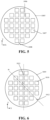
FIG. 1 is a top schematic view of a wafer of an example of the present disclosure; -
FIG. 2 is a schematic view I of a semiconductor structure of an example of the present disclosure; -
FIG. 3 is a top schematic view I of a first wafer of an example of the present disclosure; -
FIG. 4 is a top schematic view II of a first wafer of an example of the present disclosure; -
FIG. 5 is a top schematic view of a second wafer of an example of the present disclosure; -
FIG. 6 is a top schematic view I of a third wafer of an example of the present disclosure; -
FIG. 7 is a top schematic view II of a third wafer of an example of the present disclosure; -
FIG. 8 is a schematic view II of a semiconductor structure of an example of the present disclosure; -
FIG. 9 is a flow diagram of process operations of a semiconductor structure of an example of the present disclosure; and -
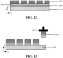
FIGs. 10-13 are schematic views of a dicing process of a semiconductor structure of an example of the present disclosure. - Implementations disclosed by the present disclosure will be described below in more detail with reference to the drawings. Although the implementations of the present disclosure are shown in the drawings, it is to be understood that the present disclosure may be achieved by various forms which should not be limited by the specific implementations as set forth herein. Rather, these implementations are provided in order to understand the present disclosure more thoroughly, and can fully convey the scope disclosed by the present disclosure to those skilled in the art.
- In the description below, many specific details are presented to provide a more thorough understanding of the present disclosure. However, it is apparent to those skilled in the art that the present disclosure may be carried out without one or more of these details. In other examples, in order to avoid confusing with the present disclosure, some technical features well-known in the art are not described; that is, not all features of actual examples are described herein, and well-known functions and structures are not described in detail.
- In the drawings, for the purpose of clarity, sizes and relative sizes of layers, areas and elements may be exaggerated. Like reference numerals denote like elements throughout.
- It should be understood that when an element or a layer is referred to as being "on", "adjacent to", "connected to", or "coupled to" other elements or layers, it may be directly on, adjacent to, connected to, or coupled to the other elements or layers, or one or more intervening elements or layers may be present. In contrast, when an element is referred to as being "directly on", "immediately adjacent to", "directly connected to", or "directly coupled to" other elements or layers, no intervening elements or layers are present. It should be understood that, although the terms first, second, third, etc., may be used to describe various elements, components, areas, layers and/or portions, these elements, components, areas, layers and/or portions should not be limited by these terms. These terms are only used to distinguish one element, component, area, layer or portion from another element, component, area, layer or portion. Thus, a first element, component, area, layer or portion discussed below may be represented as a second element, component, area, layer or portion, without departing from the teachings of the present disclosure. When the second element, component, area, layer or portion is discussed, it does not mean that the first element, component, area, layer or portion is necessarily present in the present disclosure.
- The spatially relative terms, such as "beneath", "below", "lower", "under", "over", "upper", and the like, may be used herein for ease of description to describe a relationship between one element or feature and other elements or features as illustrated in the figures. It should be understood that, the spatial relative terms are intended to further encompass different orientations of a device in use or operation in addition to the orientation depicted in the figures. For example, if a device in the drawings is turned over, then an element or a feature described as "below other elements", or "under other elements", or "beneath other elements" will be orientated to be "above" the other elements or features. Thus, the terms, "below" and "beneath", may include both upper and lower orientations. The device may be orientated otherwise (rotated by 90 degrees or other orientations), and the spatial descriptive terms used herein are interpreted accordingly.
- The terms used herein are only intended to describe the specific examples, and are not used as limitations of the present disclosure. As used herein, unless otherwise indicated expressly in the context, "a", "an" and "the" in a singular form are also intended to include a plural form. It should also be understood that the terms "consist of" and/or "comprise", when used in this specification, determine the presence of the feature, integer, step, operation, element and/or component, but do not preclude the presence or addition of one or more of other features, integers, steps, operations, elements, components, and/or groups. As used herein, the term "and/or" includes any and all combinations of the listed relevant items.
- In order to have a more detailed understanding of the features and the technical contents of the examples of the present disclosure, the implementation of the examples of the present disclosure is set forth in detail below in conjunction with the drawings, and the appended drawings are only used for reference and illustration, instead of being used to limit the examples of the present disclosure.
- With rapid development of the electronic industry, there is an increasing need for high-performance and low-cost semiconductor devices. An integration level of a traditional two-dimensional or planar memory is mainly determined by area occupied by a unit memory cell. Therefore, the integration level of the traditional two-dimensional memory is affected by a fine pattern formation technology to a great extent. However, in order to improve the pattern fineness, expensive process apparatuses are needed, which causes great limitations to increase the integration level of the two-dimensional memory. A three-dimensional memory device is an emerging type of flash memory as developed by the industry. The three-dimensional memory device solves the problem of limitations brought about by a two-dimensional or planar flash memory by stacking multiple layers of data storage cells vertically. The three-dimensional memory device has excellent precision, supports a higher storage capacity accommodated in a smaller space, is low in cost and power consumption, and can fully meet numerous requirements.
- As the requirements for the performance of the three-dimensional memory are increasingly higher, a peripheral circuit and a memory array of the three-dimensional memory tend to be bonded after being formed in different wafers. When a semiconductor structure after bonding is diced, the wafer formed with the peripheral circuit is generally selected as a wafer to be diced. As shown in
FIG. 1 , in some examples, a plurality ofperipheral circuit chips 1015 are formed in the wafer to be diced. Afirst dicing lane 1003 extending along a Y axis direction is disposed between the plurality ofperipheral circuit chips 1015. Amark 1016 is disposed at an edge of the wafer. There is a certain included angle between a pointing direction of themark 1016 and an extending direction of thefirst dicing lane 1003. The pointing direction of themark 1016 is an extending direction of a line of symmetry m of the wafer. Cleavage of the wafer is in a direction of the internal structure of the wafer where the connection strength is weak. Under an external force, a fracture easily occurs along a direction of a cleavage plane, and a smooth plane can be formed by the fracture. The cleavage plane of the wafer is parallel to the pointing direction of the mark 1016 (i.e., the extending direction of the line of symmetry m), and when there is a certain included angle between the extending direction of the line of symmetry m and the extending direction of thefirst dicing lane 1003, there is a certain included angle between the cleavage plane of the wafer and the extending direction of thefirst dicing lane 1003. Thus, the cleavage plane of the wafer (e.g., in a position where the line of symmetry m is located) passes through interiors of theperipheral circuit chips 1015, such that the wafer is prone to cleave along the cleavage plane (i.e., the interiors of the peripheral circuit chips) in a stretching process during dicing, thereby affecting the yield of the chips and having a seriously impact on the throughput of the chips. - Based on the above problem, examples of the present disclosure provide a semiconductor structure.
FIG. 2 is a schematic view of a semiconductor structure provided by examples of the present disclosure.FIG. 3 is a top schematic view of afirst wafer 1001 provided by examples of the present disclosure.FIG. 5 is a top schematic view of asecond wafer 1005 provided by examples of the present disclosure. As shown inFIGs. 2 ,3 and5 , the semiconductor structure comprises: - a
first wafer 1001, wherein thefirst wafer 1001 comprises a plurality of firstperipheral circuit chips 1002, afirst dicing lane 1003 between the firstperipheral circuit chips 1002, and afirst mark 1004 at an edge of thefirst wafer 1001, a pointing direction of thefirst mark 1004 is the same as an extending direction of thefirst dicing lane 1003, a cleavage plane of thefirst wafer 1001 is parallel to the pointing direction of thefirst mark 1004, and the pointing direction of thefirst mark 1004 is an extending direction of a line of symmetry of thefirst wafer 1001; and - a
second wafer 1005, wherein thesecond wafer 1005 and thefirst wafer 1001 are disposed in a stack, and thesecond wafer 1005 comprises a plurality ofmemory array chips 1007. - Here, the mark of the wafer generally includes two types: a notch mark and a flat mark.
FIG. 3 shows a schematic view marked with a notch mark, andFIG. 4 shows a schematic view marked with a flat mark. As shown inFIGs. 3 and 4 , the extending direction of thefirst dicing lane 1003 is, for example, a Y axis direction as shown inFIGs. 3 and 4 . The pointing direction of thefirst mark 1004 is the extending direction of the line of symmetry m of thefirst wafer 1001. The extending direction of the line of symmetry m of thefirst wafer 1001 and the extending direction of thefirst dicing lane 1003 are the same and both are the Y axis direction, while the cleavage plane of thefirst wafer 1001 is parallel to the pointing direction of thefirst mark 1004. Thus, the cleavage plane of thefirst wafer 1001 is parallel to the extending direction of thefirst dicing lane 1003. - It may be understood that, in the examples of the present disclosure, the cleavage plane of the
first wafer 1001 is parallel to the extending direction of thefirst dicing lane 1003 of thefirst wafer 1001, such that dicing may be performed from the side of thefirst wafer 1001 of the semiconductor structure during subsequent dicing of the dicing lane of the semiconductor structure, and thefirst wafer 1001 is more prone to cleave along the first dicing lane, thereby improving the problem that the firstperipheral circuit chips 1002 cleave along the interiors of the chips to affect the chip yield due to the fact that the cleavage plane of the wafer passes through the firstperipheral circuit chips 1002. - In some specific examples, the
first wafer 1001, thesecond wafer 1005, and a third wafer in the following may be, for example, wafers that have finished a process of a wafer stage (for example, a stage of forming a device structure and an interconnection structure of the device structure). - Here, the
first wafer 1001 comprises the plurality of firstperipheral circuit chips 1002, wherein each of the firstperipheral circuit chips 1002 comprises a semiconductor substrate and a peripheral device structure on the semiconductor substrate, and the peripheral device structure comprises a MOS device or other semiconductor devices. The semiconductor substrate may comprise silicon (e.g., monocrystalline silicon, c-Si), silicon germanium (SiGe), gallium arsenide (GaAs), germanium (Ge), silicon on insulator (SOI), or any other suitable materials. - In some specific examples, diameters of the
first wafer 1001, thesecond wafer 1005 and the third wafer in the following may comprise 150 mm, 200 mm, 300 mm, and 450 mm, etc., but the present disclosure is not limited thereto. - In some examples, the
memory array chips 1007 comprise three-dimensional NAND memory array chips, but the present disclosure is not limited thereto. - In some specific examples, the
memory array chips 1007 may also comprise three-dimensional NOR memory array chips, dynamic random access memory array chips, ferroelectric memory array chips, phase change memory array chips, etc., but the present disclosure is not limited thereto. - In some specific examples, the
first wafer 1001 may be bonded to thesecond wafer 1005 through a bonding process, such that the firstperipheral circuit chips 1002 in thefirst wafer 1001 are electrically connected with thememory array chips 1007 in thesecond wafer 1005. - In some specific examples, as shown in
FIG. 5 , there is athird dicing lane 1006 between the plurality ofmemory array chips 1007 of thesecond wafer 1005, and an extending direction of thethird dicing lane 1006 and the extending direction of thefirst dicing lane 1003 are the same and both are the Y axis direction, such that thememory array chips 1007 and the firstperipheral circuit chips 1002 are separated along the same direction after dicing the semiconductor structure. Thesecond wafer 1005 further comprises athird mark 1008 at an edge of thesecond wafer 1005, wherein a pointing direction of thethird mark 1008 may be the same as the extending direction of thethird dicing lane 1006, and there may be also a certain included angle between the pointing direction of thethird mark 1008 and the extending direction of thethird dicing lane 1006. - In some examples, as shown in
FIGs. 2 and6 , the semiconductor structure further comprises: thethird wafer 1009, wherein thethird wafer 1009 comprises a plurality of secondperipheral circuit chips 1010, asecond dicing lane 1011 between the secondperipheral circuit chips 1010, and asecond mark 1012 at an edge of thethird wafer 1009, and an extending direction of thesecond dicing lane 1011 and the extending direction of thefirst dicing lane 1003 are the same and both are the Y axis direction. - In some examples, as shown in
FIG. 6 , an included angle between a pointing direction of thesecond mark 1012 and the extending direction of thesecond dicing lane 1011 is a, 0° < a < 90°, and characteristic sizes of devices in the secondperipheral circuit chips 1010 are smaller than characteristic sizes of devices in the firstperipheral circuit chips 1002. The pointing direction of thesecond mark 1012 is an extending direction of a line of symmetry of thethird wafer 1009. - Here, the characteristic size refers to a minimum size of a semiconductor device in the integrated circuit field. In a complementary metal oxide semiconductor process, a typical representative of the characteristic size is a width of a "gate", i.e., a channel length of a MOS device. Generally, when the characteristic size is smaller, the integration level of the chip is higher, the performance is better, and the power consumption is lower.
- It may be understood that, when the included angle between the pointing direction of the
second mark 1012 and the extending direction of thesecond dicing lane 1011 is a, 0° < a < 90°, hole mobility of the devices formed on thethird wafer 1009 is higher, which is thus more suitable for forming peripheral circuit devices with smaller characteristic sizes and higher performance. - In examples of the present disclosure, the semiconductor structure formed in hybrid wafer stacks for dicing is formed, and the peripheral circuits are formed in two wafers. A part of devices with larger characteristic sizes are formed in the
first wafer 1001 which can act as a wafer to be diced at the same time. The other part of the devices with smaller characteristic sizes are formed in thethird wafers 1009. As such, the requirements for dicing can be met, the yield of the chips is increased, and high-performance peripheral circuit devices can be formed, thereby improving the performance of the chips. - In some examples, as shown in
FIG. 7 , the pointing direction of thesecond mark 1012 is the same as the extending direction of thesecond dicing lane 1011, a cleavage plane of thethird wafer 1009 is parallel to the pointing direction of thesecond mark 1012, and the characteristic sizes of the devices in the firstperipheral circuit chips 1002 are the same as the characteristic sizes of the devices in the secondperipheral circuit chips 1010. The pointing direction of thesecond mark 1012 is the extending direction of the line of symmetry of thethird wafer 1009. - It may be understood that, when the pointing direction of the
second mark 1012 is the same as the extending direction of thesecond dicing lane 1011, and the cleavage plane of thethird wafer 1009 is parallel to the pointing direction of thesecond mark 1012, the characteristic sizes in the secondperipheral circuit chips 1010 formed may be the same as the characteristic sizes in the firstperipheral circuit chips 1002, for example, the devices with the large characteristic sizes are formed in both the secondperipheral circuit chips 1010 and the firstperipheral circuit chips 1002. - In examples of the present disclosure, there are several relative position relationships of the
first wafer 1001, thesecond wafer 1005 and thethird wafer 1009. - In some examples, as shown in
FIG. 8 , thethird wafer 1009 is located between thefirst wafer 1001 and thesecond wafer 1005. - In some examples, as shown in
FIG. 2 , thesecond wafer 1005 is located between thefirst wafer 1001 and thethird wafer 1009. - It may be understood that, when the pointing direction of the
second mark 1012 is the same as the extending direction of thesecond dicing lane 1011, and the cleavage plane of thethird wafer 1009 is parallel to the pointing direction of thesecond mark 1012, the cleavage plane of thethird wafer 1009 is parallel to the extending direction of thesecond dicing lane 1011 of thethird wafer 1009, such that thethird wafer 1009 is also suitable for dicing. Thesecond wafer 1005 is located between thefirst wafer 1001 and thethird wafer 1009, such that the semiconductor structure can be diced from the side of thefirst wafer 1001 and the side of thethird wafer 1009 at the same time, which can meet process requirements of simultaneous two-side dicing and improve subsequent dicing efficiency. - Examples of the present disclosure provide a semiconductor structure comprising: a
first wafer 1001, wherein thefirst wafer 1001 comprises a plurality of firstperipheral circuit chips 1002, afirst dicing lane 1003 between the firstperipheral circuit chips 1002, and afirst mark 1004 at an edge of thefirst wafer 1001, a pointing direction of thefirst mark 1004 is the same as an extending direction of thefirst dicing lane 1003, a cleavage plane of thefirst wafer 1001 is parallel to the pointing direction of thefirst mark 1004, and the pointing direction of thefirst mark 1004 is an extending direction of a line of symmetry of thefirst wafer 1001; and asecond wafer 1005, wherein thesecond wafer 1005 and thefirst wafer 1001 are disposed in a stack, and thesecond wafer 1005 comprises a plurality ofmemory array chips 1007. In examples of the present disclosure, the pointing direction of thefirst mark 1004 is the same as the extending direction of thefirst dicing lane 1003, and the cleavage plane of thefirst wafer 1001 is parallel to the pointing direction of thefirst mark 1004, such that the cleavage plane of thefirst wafer 1001 is parallel to the extending direction of thefirst dicing lane 1003 of thefirst wafer 1001. As such, dicing may be performed from the side offirst wafer 1001 of the semiconductor structure during subsequent dicing of the semiconductor structure, and thefirst wafer 1001 is more prone to cleave along a direction of the first dicing lane, thereby improving the problem that the firstperipheral circuit chips 1002 cleave along the interiors of the chips to affect the chip yield due to the fact that the cleavage plane of the wafer passes through the interiors of the firstperipheral circuit chips 1002 when there is a certain included angle between the cleavage plane and the dicing lane of the wafer. - Based on the above-mentioned semiconductor structure, examples of the present disclosure further provide a dicing method of a semiconductor structure. As shown in
FIG. 9 , the method comprises: - operation S1001: providing a semiconductor structure to be diced, wherein the semiconductor structure to be diced comprises a
first wafer 1001 and asecond wafer 1005; thefirst wafer 1001 comprises a plurality of first peripheral circuit chips, a first dicing lane between the first peripheral circuit chips, and a first mark at an edge of thefirst wafer 1001, a pointing direction of the first mark is the same as an extending direction of the first dicing lane, and a cleavage plane of thefirst wafer 1001 is parallel to the pointing direction of the first mark; thesecond wafer 1005 and thefirst wafer 1001 are disposed in a stack, and thesecond wafer 1005 comprises a plurality of memory array chips; and the pointing direction of the first mark is an extending direction of a line of symmetry of thefirst wafer 1001; - operation S1002: dicing the first dicing lane from a side of the
first wafer 1001 away from thesecond wafer 1005; and - operation S1003: stretching the semiconductor structure to be diced, such that the cleavage plane of the
first wafer 1001 extends to thesecond wafer 1005. - The dicing method of the semiconductor structure will be further introduced below in conjunction with
FIGs. 10-13 . - In operation S1001, as shown in
FIG. 10 , the semiconductor structure to be diced is provided, and the semiconductor structure to be diced has been introduced in detail in the above introduction of the semiconductor structure, which is no longer repeated here. - In some examples, the providing the semiconductor structure to be diced comprises:
- providing the
first wafer 1001 comprising the plurality of first peripheral circuit chips; - providing the
second wafer 1005 comprising the plurality of memory array chips; and - bonding the
first wafer 1001 to thesecond wafer 1005 to form the semiconductor structure to be diced. - In some specific examples, after providing the semiconductor structure to be diced, the method further comprises: providing a
carrier wafer 1013, and disposing the semiconductor structure to be diced on thecarrier wafer 1013, with thefirst wafer 1001 in the semiconductor structure to be diced facing away from thecarrier wafer 1013. - In operation S1002, as shown in
FIG. 11 , the first dicing lane is diced. - Here, the first dicing lane is diced from the side of the
first wafer 1001 away from thesecond wafer 1005. It may be understood that, as shown inFIG. 11 , the first dicing lane of thefirst wafer 1001 is diced from the side of thefirst wafer 1001. - It may be understood that, in examples of the present disclosure, the pointing direction of the first mark is the same as the extending direction of the first dicing lane, and the cleavage plane of the
first wafer 1001 is parallel to the pointing direction of the first mark, such that the cleavage plane of thefirst wafer 1001 is parallel to the extending direction of the first dicing lane of thefirst wafer 1001. As such, the dicing may be performed from the side of thefirst wafer 1001 of the semiconductor structure during the subsequent dicing of the semiconductor structure to be diced, and thefirst wafer 1001 is more prone to cleave along a direction of the first dicing lane, thereby improving the problem that the first peripheral circuit chips cleave along the interiors of the chips to affect the chip yield due to the fact that the cleavage plane of the wafer passes through the interiors of the first peripheral circuit chips when there is a certain included angle between the cleavage plane and the dicing lane of the wafer. - In some examples, the dicing the first dicing lane of the
first wafer 1001 from the side of thefirst wafer 1001 away from thesecond wafer 1005 comprises:
dicing the first dicing lane of thefirst wafer 1001 from the side of thefirst wafer 1001 away from thesecond wafer 1005 by using a laser dicing process. - In operation S1003, as shown in
FIG. 12 , the semiconductor structure to be diced is stretched, such that the cleavage plane of thefirst wafer 1001 extends to thesecond wafer 1005. - In some specific examples, there is a third dicing lane between the plurality of memory array chips of the
second wafer 1005, and an extending direction of the third dicing lane is the same as the extending direction of the first dicing lane. After stretching the semiconductor structure to be diced, the cleavage plane of thefirst wafer 1001 extends to thesecond wafer 1005. The cleavage plane of thefirst wafer 1001 is parallel to the extending direction of the first dicing lane, and the extending direction of the third dicing lane is the same as the extending direction of the first dicing lane. Thus, the cleavage plane extending to thesecond wafer 1005 is parallel to the extending direction of the third dicing lane, such that thesecond wafer 1005 cleaves along a direction of the third dicing lane, thereby enabling an increase of the dicing yield of the chips. - In some examples, the semiconductor structure further comprises: a
third wafer 1009, wherein thethird wafer 1009 comprises a plurality of second peripheral circuit chips, a second dicing lane between the second peripheral circuit chips, and a second mark at an edge of thethird wafer 1009, and an extending direction of the second dicing lane is the same as the extending direction of the first dicing lane. - In some examples, an included angle between a pointing direction of the second mark and the extending direction of the second dicing lane is a, 0° < a < 90°, and characteristic sizes of devices in the second peripheral circuit chips are smaller than characteristic sizes of devices in the first peripheral circuit chips; the pointing direction of the second mark is an extending direction of a line of symmetry of the
third wafer 1009; and
the stretching the semiconductor structure to be diced such that the cleavage plane of thefirst wafer 1001 extends to thesecond wafer 1005 comprises:
stretching the semiconductor structure to be diced, such that the cleavage plane of thefirst wafer 1001 extends to thesecond wafer 1005 and thethird wafer 1009. - It may be understood that, the
first wafer 1001 is used as a wafer to be diced, while thethird wafer 1009 is mainly used for forming high-performance peripheral circuit devices, such that the yield problem during the dicing of the semiconductor structure can be improved, and the high-performance peripheral circuit devices can also be formed. - In some examples, the pointing direction of the second mark is the same as the extending direction of the second dicing lane, a cleavage plane of the
third wafer 1009 is parallel to the pointing direction of the second mark, and the characteristic sizes of the devices in the first peripheral circuit chips are the same as the characteristic sizes of the devices in the second peripheral circuit chips; the pointing direction of the second mark is the extending direction of the line of symmetry of thethird wafer 1009; and thesecond wafer 1005 is located between thefirst wafer 1001 and thethird wafer 1009;
the method further comprises: - dicing the second dicing lane from a side of the
third wafer 1009 away from thesecond wafer 1005 while dicing the first dicing lane from the side of thefirst wafer 1001 away from thesecond wafer 1005; and - stretching the semiconductor structure to be diced such that the cleavage plane of the
first wafer 1001 extends to thesecond wafer 1005 comprises:
stretching the semiconductor structure to be diced, such that the cleavage plane of thefirst wafer 1001 and the cleavage plane of thethird wafer 1009 extend to thesecond wafer 1005. - It may be understood that, when the pointing direction of the second mark is the same as the extending direction of the second dicing lane, and the cleavage plane of the
third wafer 1009 is parallel to the pointing direction of the second mark, the cleavage plane of thethird wafer 1009 is parallel to the extending direction of the second dicing lane of thethird wafer 1009, such that thethird wafer 1009 is also suitable for dicing. Thesecond wafer 1005 is located between thefirst wafer 1001 and thethird wafer 1009, such that the semiconductor structure can be diced from the side of thefirst wafer 1001 and the side of thethird wafer 1009 simultaneously, and then the semiconductor structure to be diced is stretched, such that the cleavage plane of thefirst wafer 1001 and the cleavage plane of thethird wafer 1009 both extend to thesecond wafer 1005, thereby separating thesecond wafer 1005 along the third dicing lane. As such, the process requirement of simultaneous two-side dicing can be met, the dicing efficiency is improved, and the yield of the chips after the dicing can also be increased. - In some specific examples, the semiconductor structure to be diced can be diced using a wafer dicing device as following. The wafer dicing device comprises: a carrier table, a first dicing sub-device and a second dicing sub-device, wherein the carrier table is configured to carry a wafer to be diced; the first dicing sub-device is configured to dice the wafer to be diced from a first side; the second dicing sub-device is configured to dice the wafer to be diced from a second side; and the first side and the second side are two opposite sides of the carrier table along a first direction that is a thickness direction of the carrier table.
- It may be understood that, the wafer dicing device comprises the first dicing sub-device and the second dicing sub-device which are respectively configured to dice the semiconductor structure to be diced from the two sides of the thickness direction of the carrier table. On the one hand, front side and back side dicing of the semiconductor structure to be diced can be achieved simultaneously, which can improve the dicing efficiency; on the other hand, since the front side and the back side of the semiconductor structure to be diced can be diced simultaneously, components of the first dicing sub-device and the second dicing sub-device can be disposed correspondingly, thereby improving the problem that front side and back side dicing positions are difficult to align in a process of dicing the front side and the back side of the semiconductor structure to be diced separately, which can further effectively increase the yield of the chips after dicing.
- In some specific examples, the semiconductor structure to be diced can be placed on the carrier table; the semiconductor structure to be diced is diced from the first side by using the first dicing sub-device, and the semiconductor structure to be diced is diced from the second side by using the second dicing sub-device; and the first side and the second side are two opposite sides of the carrier table along the first direction that is the thickness direction of the carrier table.
- In some examples, the pointing direction of the second mark is the same as the extending direction of the second dicing lane, a cleavage plane of the
third wafer 1009 is parallel to the pointing direction of the second mark, and the characteristic sizes of the devices in the first peripheral circuit chips are the same as the characteristic sizes of the devices in the second peripheral circuit chips; the pointing direction of the second mark is the extending direction of the line of symmetry of thethird wafer 1009; thethird wafer 1009 is located between thefirst wafer 1001 and thesecond wafer 1005;
the dicing the first dicing lane from the side of thefirst wafer 1001 away from thesecond wafer 1005 comprises: - dicing the first dicing lane and the second dicing lane from the side of the
first wafer 1001 away from thesecond wafer 1005; and - stretching the semiconductor structure to be diced such that the cleavage plane of the
first wafer 1001 extends to thesecond wafer 1005 comprises:
stretching the semiconductor structure to be diced, such that the cleavage plane of thefirst wafer 1001 and the cleavage plane of thethird wafer 1009 extend to thesecond wafer 1005. - It may be understood that, the
third wafer 1009 is located between thefirst wafer 1001 and thesecond wafer 1005, the cleavage plane of thefirst wafer 1001 is parallel to the extending direction of the first dicing lane, and the cleavage plane of thethird wafer 1009 is parallel to the extending direction of the second dicing lane. Thus, both thefirst wafer 1001 and thethird wafer 1009 can be diced from the side of thefirst wafer 1001 by using a laser dicing process, and then the semiconductor structure to be diced is stretched, such that both the cleavage plane of thefirst wafer 1001 and the cleavage plane of thethird wafer 1009 extend to thesecond wafer 1005, thereby separating thesecond wafer 1005 along the third dicing lane. - In some examples, the stretching the semiconductor structure to be diced comprises:
stretching the semiconductor structure to be diced along a direction perpendicular to the cleavage plane of thefirst wafer 1001. - In some specific examples, the stretching may be along an X axis direction as shown in
FIG. 12 , but the stretching direction of the semiconductor structure is not limited thereto. - It may be understood that, the positions of the wafer cleavage planes are positions that are prone to fracture, and when the semiconductor structure to be diced is stretched, the wafers are more likely to cleave along the cleavage planes if the stretching is performed along a direction perpendicular to the cleavage plane of the
first wafer 1001. - In some specific examples, as shown in
FIG. 13 , after the dicing operation is finished for the wafer to be diced,individual memories 1014 are formed, and the separatedmemories 1014 can be taken from thecarrier wafer 1013 by using a device with arobotic arm 1017. - Based on the above dicing method of the semiconductor structure, examples of the present disclosure further provide a memory which is obtained by dicing the semiconductor structure by using the dicing method of any one of the above examples.
- It is to be understood that, references to "one example" or "an example" throughout this specification mean that particular features, structures, or characteristics related to the example are included in at least one example of the present disclosure. Therefore, "in one example" or "in an example" presented throughout this specification does not necessarily refer to the same example. Furthermore, these particular features, structures, or characteristics may be incorporated in one or more examples in any suitable manner. It is to be understood that, in various examples of the present disclosure, sequence numbers of the above processes do not indicate an execution sequence, and an execution sequence of the processes shall be determined by functionalities and intrinsic logics thereof, and shall constitute no limitation on implementation processes of the examples of the present disclosure. The above sequence numbers of the examples of the present disclosure are only for description, and do not represent advantages or disadvantages of the examples.
- The methods disclosed in several method examples as provided by the present disclosure may be combined freely to obtain new method examples in case of no conflicts.
- The above descriptions are merely specific implementations of the present disclosure, and the protection scope of the present disclosure is not limited to these. Any variation or replacement that may be readily figured out by those skilled in the art within the technical scope disclosed by the present disclosure shall fall within the protection scope of the present disclosure. Thus, the protection scope of the present disclosure shall be defined by the protection scope of the claims.
Claims (16)
- A semiconductor structure, comprising:a first wafer comprising:a plurality of first peripheral circuit chips;a first dicing lane between the first peripheral circuit chips; anda first mark at an edge of the first wafer,wherein a pointing direction of the first mark is the same as an extending direction of the first dicing lane, a cleavage plane of the first wafer is parallel to the pointing direction of the first mark, and the pointing direction of the first mark is an extending direction of a line of symmetry of the first wafer; anda second wafer, wherein the second wafer and the first wafer are disposed in a stack, and the second wafer comprises a plurality of memory array chips.
- The semiconductor structure of claim 1, further comprising:
a third wafer comprising:a plurality of second peripheral circuit chips;a second dicing lane between the second peripheral circuit chips; anda second mark at an edge of the third wafer,wherein an extending direction of the second dicing lane is the same as the extending direction of the first dicing lane. - The semiconductor structure of claim 2, wherein an included angle between a pointing direction of the second mark and the extending direction of the second dicing lane is a, 0° < a < 90°, and characteristic sizes of devices in the second peripheral circuit chips are smaller than characteristic sizes of devices in the first peripheral circuit chips; and the pointing direction of the second mark is an extending direction of a line of symmetry of the third wafer.
- The semiconductor structure of claim 2, wherein a pointing direction of the second mark is the same as the extending direction of the second dicing lane, a cleavage plane of the third wafer is parallel to the pointing direction of the second mark, and characteristic sizes of devices in the first peripheral circuit chips are the same as characteristic sizes of devices in the second peripheral circuit chips; and the pointing direction of the second mark is an extending direction of a line of symmetry of the third wafer.
- The semiconductor structure of claim 2, wherein the third wafer is located between the first wafer and the second wafer.
- The semiconductor structure of claim 2, wherein the second wafer is located between the first wafer and the third wafer.
- The semiconductor structure of claim 1, wherein the memory array chips comprise three-dimensional NAND memory array chips.
- A dicing method of a semiconductor structure, comprising:providing a semiconductor structure to be diced, wherein the semiconductor structure to be diced comprises a first wafer and a second wafer; the first wafer comprises a plurality of first peripheral circuit chips, a first dicing lane between the first peripheral circuit chips, and a first mark at an edge of the first wafer, a pointing direction of the first mark is the same as an extending direction of the first dicing lane, and a cleavage plane of the first wafer is parallel to the pointing direction of the first mark; the second wafer and the first wafer are disposed in a stack, and the second wafer comprises a plurality of memory array chips; and the pointing direction of the first mark is an extending direction of a line of symmetry of the first wafer;dicing the first dicing lane from a side of the first wafer away from the second wafer; andstretching the semiconductor structure to be diced, such that the cleavage plane of the first wafer extends to the second wafer.
- The dicing method of claim 8, wherein the dicing the first dicing lane of the first wafer from the side of the first wafer away from the second wafer comprises:
dicing the first dicing lane of the first wafer from the side of the first wafer away from the second wafer by using a laser dicing process. - The dicing method of claim 8, wherein the semiconductor structure further comprises: a third wafer, wherein the third wafer comprises a plurality of second peripheral circuit chips, a second dicing lane between the second peripheral circuit chips, and a second mark at an edge of the third wafer, and an extending direction of the second dicing lane is the same as the extending direction of the first dicing lane.
- The dicing method of claim 10, wherein an included angle between a pointing direction of the second mark and the extending direction of the second dicing lane is a, 0° < a < 90°, and characteristic sizes of devices in the second peripheral circuit chips are smaller than characteristic sizes of devices in the first peripheral circuit chips; the pointing direction of the second mark is an extending direction of a line of symmetry of the third wafer; and
the stretching the semiconductor structure to be diced such that the cleavage plane of the first wafer extends to the second wafer comprises:
stretching the semiconductor structure to be diced, such that the cleavage plane of the first wafer extends to the second wafer and the third wafer. - The dicing method of claim 10, wherein a pointing direction of the second mark is the same as the extending direction of the second dicing lane, a cleavage plane of the third wafer is parallel to the pointing direction of the second mark, and characteristic sizes of devices in the first peripheral circuit chips are the same as characteristic sizes of devices in the second peripheral circuit chips; the pointing direction of the second mark is an extending direction of a line of symmetry of the third wafer; the second wafer is located between the first wafer and the third wafer;the method further comprises:
dicing the second dicing lane from a side of the third wafer away from the second wafer while dicing the first dicing lane from the side of the first wafer away from the second wafer; andstretching the semiconductor structure to be diced such that the cleavage plane of the first wafer extends to the second wafer comprises:
stretching the semiconductor structure to be diced, such that the cleavage plane of the first wafer and the cleavage plane of the third wafer extend to the second wafer. - The dicing method of claim 10, wherein a pointing direction of the second mark is the same as the extending direction of the second dicing lane, a cleavage plane of the third wafer is parallel to the pointing direction of the second mark, and characteristic sizes of devices in the first peripheral circuit chips are the same as characteristic sizes of devices in the second peripheral circuit chips; the pointing direction of the second mark is an extending direction of a line of symmetry of the third wafer; the third wafer is located between the first wafer and the second wafer;the dicing the first dicing lane from the side of the first wafer away from the second wafer comprises:
dicing the first dicing lane and the second dicing lane from the side of the first wafer away from the second wafer; andstretching the semiconductor structure to be diced such that the cleavage plane of the first wafer extends to the second wafer comprises:
stretching the semiconductor structure to be diced, such that the cleavage plane of the first wafer and the cleavage plane of the third wafer extend to the second wafer. - The dicing method of claim 8, wherein the stretching the semiconductor structure to be diced comprises:
stretching the semiconductor structure to be diced along a direction perpendicular to the cleavage plane of the first wafer. - The dicing method of claim 8, wherein the providing the semiconductor structure to be diced comprises:providing the first wafer comprising the plurality of first peripheral circuit chips;providing the second wafer comprising the plurality of memory array chips; andbonding the first wafer to the second wafer to form the semiconductor structure to be diced.
- A memory, wherein the memory is obtained by dicing the semiconductor structure by using the dicing method of any one of claims 8-15.
Applications Claiming Priority (1)
| Application Number | Priority Date | Filing Date | Title |
|---|---|---|---|
| PCT/CN2023/093931 WO2024234150A1 (en) | 2023-05-12 | 2023-05-12 | Semiconductor structure and cutting method therefor, and memory |
Publications (2)
| Publication Number | Publication Date |
|---|---|
| EP4485505A1 true EP4485505A1 (en) | 2025-01-01 |
| EP4485505A4 EP4485505A4 (en) | 2025-10-22 |
Family
ID=93380151
Family Applications (1)
| Application Number | Title | Priority Date | Filing Date |
|---|---|---|---|
| EP23923196.2A Pending EP4485505A4 (en) | 2023-05-12 | 2023-05-12 | SEMICONDUCTOR STRUCTURE AND DIVISION METHOD THEREFOR AND STORAGE |
Country Status (6)
| Country | Link |
|---|---|
| US (1) | US20240379578A1 (en) |
| EP (1) | EP4485505A4 (en) |
| JP (1) | JP2025519993A (en) |
| KR (1) | KR20240166473A (en) |
| CN (1) | CN119585861A (en) |
| WO (1) | WO2024234150A1 (en) |
Family Cites Families (20)
| Publication number | Priority date | Publication date | Assignee | Title |
|---|---|---|---|---|
| JP2001250799A (en) * | 2000-03-03 | 2001-09-14 | Mitsubishi Electric Corp | Semiconductor wafer and semiconductor device |
| US6528393B2 (en) * | 2000-06-13 | 2003-03-04 | Advanced Semiconductor Engineering, Inc. | Method of making a semiconductor package by dicing a wafer from the backside surface thereof |
| JP2004260083A (en) * | 2003-02-27 | 2004-09-16 | Nippon Sheet Glass Co Ltd | Wafer cutting method and light emitting element array chip |
| JP2007317935A (en) * | 2006-05-26 | 2007-12-06 | Canon Inc | Semiconductor substrate, substrate cleaving method, and element chip manufacturing method |
| JP2013062372A (en) * | 2011-09-13 | 2013-04-04 | Fukuoka Univ | Device wafer and method for cutting device wafer |
| US9029234B2 (en) * | 2012-05-15 | 2015-05-12 | International Business Machines Corporation | Physical design symmetry and integrated circuits enabling three dimentional (3D) yield optimization for wafer to wafer stacking |
| JP6455166B2 (en) * | 2015-01-16 | 2019-01-23 | 富士電機株式会社 | Manufacturing method of semiconductor wafer and semiconductor chip |
| JP6896337B2 (en) * | 2017-06-01 | 2021-06-30 | 株式会社ディスコ | Processing method for fan-shaped wafer pieces |
| CN211907412U (en) * | 2018-05-17 | 2020-11-10 | 北京世纪金光半导体有限公司 | Wafer |
| US10290612B1 (en) * | 2018-05-30 | 2019-05-14 | Invensas Corporation | Systems and methods for flash stacking |
| US10734285B2 (en) * | 2018-06-28 | 2020-08-04 | Taiwan Semiconductor Manufacturing Co., Ltd. | Bonding support structure (and related process) for wafer stacking |
| CN111223949A (en) * | 2018-11-23 | 2020-06-02 | 成都晔凡科技有限公司 | Single crystal cell cutting method, single crystal cell, photovoltaic module and preparation method |
| CN113169125B (en) * | 2019-01-31 | 2024-05-28 | 桑迪士克科技有限责任公司 | Warp compensated bonding structure including support chip and three-dimensional memory chip |
| KR20200102055A (en) * | 2019-02-21 | 2020-08-31 | 삼성전자주식회사 | Semiconductor package with silicon crystal structure |
| CN111710646B (en) * | 2020-05-15 | 2021-06-01 | 长江存储科技有限责任公司 | Polycrystalline circle scribing method and semiconductor structure |
| US11682652B2 (en) * | 2021-03-10 | 2023-06-20 | Taiwan Semiconductor Manufacturing Company, Ltd. | Notched wafer and bonding support structure to improve wafer stacking |
| JP7650691B2 (en) * | 2021-03-22 | 2025-03-25 | 株式会社ディスコ | Stacked wafer processing method |
| US11832520B2 (en) * | 2021-04-27 | 2023-11-28 | Taiwan Semiconductor Manufacturing Company, Ltd. | Voltage breakdown uniformity in piezoelectric structure for piezoelectric devices |
| JP7636118B2 (en) * | 2021-07-15 | 2025-02-26 | 株式会社ディスコ | Method for forming a stacked device wafer |
| JP2023110311A (en) * | 2022-01-28 | 2023-08-09 | 浜松ホトニクス株式会社 | LASER PROCESSING METHOD AND LASER PROCESSING APPARATUS |
-
2023
- 2023-05-12 KR KR1020247029075A patent/KR20240166473A/en active Pending
- 2023-05-12 CN CN202380009222.7A patent/CN119585861A/en active Pending
- 2023-05-12 JP JP2024551595A patent/JP2025519993A/en active Pending
- 2023-05-12 EP EP23923196.2A patent/EP4485505A4/en active Pending
- 2023-05-12 WO PCT/CN2023/093931 patent/WO2024234150A1/en not_active Ceased
- 2023-10-17 US US18/381,030 patent/US20240379578A1/en active Pending
Also Published As
| Publication number | Publication date |
|---|---|
| EP4485505A4 (en) | 2025-10-22 |
| US20240379578A1 (en) | 2024-11-14 |
| CN119585861A (en) | 2025-03-07 |
| JP2025519993A (en) | 2025-07-01 |
| WO2024234150A1 (en) | 2024-11-21 |
| KR20240166473A (en) | 2024-11-26 |
Similar Documents
| Publication | Publication Date | Title |
|---|---|---|
| JP7311615B2 (en) | Junction semiconductor device with processor and NAND flash memory and method of forming same | |
| US8564106B2 (en) | Wafer level packaging | |
| CN114664788B (en) | Die stitching and harvesting of array structures | |
| EP3891806B1 (en) | Unified semiconductor devices having processor and heterogeneous memories and methods for forming the same | |
| US8242543B2 (en) | Semiconductor wafer-to-wafer bonding for dissimilar semiconductor dies and/or wafers | |
| CN1052114C (en) | Method for producing single chip electronic device by way of piling IC chip plane array | |
| TWI397132B (en) | Fabrication of three dimensional integrated circuit employing multiple die panels | |
| US9698268B2 (en) | Methods of forming semiconductor devices, including forming a semiconductor material on a fin, and related semiconductor devices | |
| US9893018B2 (en) | Alignment mark for semiconductor device | |
| US20200365539A1 (en) | Bonding Structure And Method For Manufacturing The Same | |
| KR20260038301A (en) | Pad structures for semiconductor devices | |
| CN111863784B (en) | Semiconductor structure and manufacturing method thereof | |
| WO2023231188A1 (en) | Memory and preparation method therefor | |
| WO2024006594A1 (en) | Microelectronic assemblies including stacked dies coupled by a through dielectric via | |
| EP4485505A1 (en) | Semiconductor structure and cutting method therefor, and memory | |
| CN120453233A (en) | Semiconductor device and cutting method thereof, semiconductor chip | |
| JP3660904B2 (en) | Manufacturing method of three-dimensional circuit | |
| CN114512490B (en) | A memory and a method for preparing the same | |
| US20240079272A1 (en) | Method of manufacturing semiconductor chip including forming dicing grooves and semiconductor device | |
| JP2024517175A (en) | Three-dimensional memory, chip package structure, and electronic device | |
| US20240355689A1 (en) | Stacked layers with filling structures | |
| US20250311437A1 (en) | Inter-die connectivity with a backend switch | |
| US20240375212A1 (en) | Wafer dicing devices and methods of wafer dicing | |
| US20240222184A1 (en) | Semiconductor substrate with a sacrificial annulus | |
| US20250081451A1 (en) | Semiconductor structure, forming method thereof and semiconductor device |
Legal Events
| Date | Code | Title | Description |
|---|---|---|---|
| STAA | Information on the status of an ep patent application or granted ep patent |
Free format text: STATUS: UNKNOWN |
|
| STAA | Information on the status of an ep patent application or granted ep patent |
Free format text: STATUS: THE INTERNATIONAL PUBLICATION HAS BEEN MADE |
|
| PUAI | Public reference made under article 153(3) epc to a published international application that has entered the european phase |
Free format text: ORIGINAL CODE: 0009012 |
|
| STAA | Information on the status of an ep patent application or granted ep patent |
Free format text: STATUS: REQUEST FOR EXAMINATION WAS MADE |
|
| 17P | Request for examination filed |
Effective date: 20240826 |
|
| AK | Designated contracting states |
Kind code of ref document: A1 Designated state(s): AL AT BE BG CH CY CZ DE DK EE ES FI FR GB GR HR HU IE IS IT LI LT LU LV MC ME MK MT NL NO PL PT RO RS SE SI SK SM TR |
|
| A4 | Supplementary search report drawn up and despatched |
Effective date: 20250923 |
|
| RIC1 | Information provided on ipc code assigned before grant |
Ipc: H01L 21/304 20060101AFI20250917BHEP Ipc: H01L 21/78 20060101ALI20250917BHEP Ipc: H01L 23/544 20060101ALI20250917BHEP |
|
| STAA | Information on the status of an ep patent application or granted ep patent |
Free format text: STATUS: EXAMINATION IS IN PROGRESS |
|
| 17Q | First examination report despatched |
Effective date: 20260202 |