EP4485217A1 - Host, information processing method, electronic system, and readable storage medium - Google Patents
Host, information processing method, electronic system, and readable storage medium Download PDFInfo
- Publication number
- EP4485217A1 EP4485217A1 EP23923204.4A EP23923204A EP4485217A1 EP 4485217 A1 EP4485217 A1 EP 4485217A1 EP 23923204 A EP23923204 A EP 23923204A EP 4485217 A1 EP4485217 A1 EP 4485217A1
- Authority
- EP
- European Patent Office
- Prior art keywords
- host
- request
- cpu core
- memory
- thread
- Prior art date
- Legal status (The legal status is an assumption and is not a legal conclusion. Google has not performed a legal analysis and makes no representation as to the accuracy of the status listed.)
- Pending
Links
Images






Classifications
-
- G—PHYSICS
- G06—COMPUTING OR CALCULATING; COUNTING
- G06F—ELECTRIC DIGITAL DATA PROCESSING
- G06F13/00—Interconnection of, or transfer of information or other signals between, memories, input/output devices or central processing units
- G06F13/10—Program control for peripheral devices
- G06F13/105—Program control for peripheral devices where the program performs an input/output emulation function
-
- G—PHYSICS
- G06—COMPUTING OR CALCULATING; COUNTING
- G06F—ELECTRIC DIGITAL DATA PROCESSING
- G06F13/00—Interconnection of, or transfer of information or other signals between, memories, input/output devices or central processing units
- G06F13/14—Handling requests for interconnection or transfer
- G06F13/16—Handling requests for interconnection or transfer for access to memory bus
- G06F13/1668—Details of memory controller
-
- G—PHYSICS
- G06—COMPUTING OR CALCULATING; COUNTING
- G06F—ELECTRIC DIGITAL DATA PROCESSING
- G06F13/00—Interconnection of, or transfer of information or other signals between, memories, input/output devices or central processing units
- G06F13/10—Program control for peripheral devices
- G06F13/102—Program control for peripheral devices where the program performs an interfacing function, e.g. device driver
-
- G—PHYSICS
- G06—COMPUTING OR CALCULATING; COUNTING
- G06F—ELECTRIC DIGITAL DATA PROCESSING
- G06F13/00—Interconnection of, or transfer of information or other signals between, memories, input/output devices or central processing units
- G06F13/14—Handling requests for interconnection or transfer
- G06F13/16—Handling requests for interconnection or transfer for access to memory bus
- G06F13/1605—Handling requests for interconnection or transfer for access to memory bus based on arbitration
- G06F13/1652—Handling requests for interconnection or transfer for access to memory bus based on arbitration in a multiprocessor architecture
-
- G—PHYSICS
- G06—COMPUTING OR CALCULATING; COUNTING
- G06F—ELECTRIC DIGITAL DATA PROCESSING
- G06F13/00—Interconnection of, or transfer of information or other signals between, memories, input/output devices or central processing units
- G06F13/14—Handling requests for interconnection or transfer
- G06F13/16—Handling requests for interconnection or transfer for access to memory bus
- G06F13/1668—Details of memory controller
- G06F13/1673—Details of memory controller using buffers
-
- G—PHYSICS
- G06—COMPUTING OR CALCULATING; COUNTING
- G06F—ELECTRIC DIGITAL DATA PROCESSING
- G06F13/00—Interconnection of, or transfer of information or other signals between, memories, input/output devices or central processing units
- G06F13/14—Handling requests for interconnection or transfer
- G06F13/20—Handling requests for interconnection or transfer for access to input/output bus
-
- G—PHYSICS
- G06—COMPUTING OR CALCULATING; COUNTING
- G06F—ELECTRIC DIGITAL DATA PROCESSING
- G06F13/00—Interconnection of, or transfer of information or other signals between, memories, input/output devices or central processing units
- G06F13/14—Handling requests for interconnection or transfer
- G06F13/20—Handling requests for interconnection or transfer for access to input/output bus
- G06F13/22—Handling requests for interconnection or transfer for access to input/output bus using successive scanning, e.g. polling
-
- G—PHYSICS
- G06—COMPUTING OR CALCULATING; COUNTING
- G06F—ELECTRIC DIGITAL DATA PROCESSING
- G06F13/00—Interconnection of, or transfer of information or other signals between, memories, input/output devices or central processing units
- G06F13/14—Handling requests for interconnection or transfer
- G06F13/20—Handling requests for interconnection or transfer for access to input/output bus
- G06F13/24—Handling requests for interconnection or transfer for access to input/output bus using interrupt
-
- G—PHYSICS
- G06—COMPUTING OR CALCULATING; COUNTING
- G06F—ELECTRIC DIGITAL DATA PROCESSING
- G06F13/00—Interconnection of, or transfer of information or other signals between, memories, input/output devices or central processing units
- G06F13/14—Handling requests for interconnection or transfer
- G06F13/36—Handling requests for interconnection or transfer for access to common bus or bus system
- G06F13/362—Handling requests for interconnection or transfer for access to common bus or bus system with centralised access control
- G06F13/366—Handling requests for interconnection or transfer for access to common bus or bus system with centralised access control using a centralised polling arbiter
-
- G—PHYSICS
- G06—COMPUTING OR CALCULATING; COUNTING
- G06F—ELECTRIC DIGITAL DATA PROCESSING
- G06F15/00—Digital computers in general; Data processing equipment in general
- G06F15/16—Combinations of two or more digital computers each having at least an arithmetic unit, a program unit and a register, e.g. for a simultaneous processing of several programs
- G06F15/163—Interprocessor communication
- G06F15/167—Interprocessor communication using a common memory, e.g. mailbox
-
- G—PHYSICS
- G06—COMPUTING OR CALCULATING; COUNTING
- G06F—ELECTRIC DIGITAL DATA PROCESSING
- G06F3/00—Input arrangements for transferring data to be processed into a form capable of being handled by the computer; Output arrangements for transferring data from processing unit to output unit, e.g. interface arrangements
- G06F3/06—Digital input from, or digital output to, record carriers, e.g. RAID, emulated record carriers or networked record carriers
- G06F3/0601—Interfaces specially adapted for storage systems
- G06F3/0602—Interfaces specially adapted for storage systems specifically adapted to achieve a particular effect
- G06F3/061—Improving I/O performance
-
- G—PHYSICS
- G06—COMPUTING OR CALCULATING; COUNTING
- G06F—ELECTRIC DIGITAL DATA PROCESSING
- G06F3/00—Input arrangements for transferring data to be processed into a form capable of being handled by the computer; Output arrangements for transferring data from processing unit to output unit, e.g. interface arrangements
- G06F3/06—Digital input from, or digital output to, record carriers, e.g. RAID, emulated record carriers or networked record carriers
- G06F3/0601—Interfaces specially adapted for storage systems
- G06F3/0628—Interfaces specially adapted for storage systems making use of a particular technique
- G06F3/0655—Vertical data movement, i.e. input-output transfer; data movement between one or more hosts and one or more storage devices
- G06F3/0659—Command handling arrangements, e.g. command buffers, queues, command scheduling
-
- G—PHYSICS
- G06—COMPUTING OR CALCULATING; COUNTING
- G06F—ELECTRIC DIGITAL DATA PROCESSING
- G06F3/00—Input arrangements for transferring data to be processed into a form capable of being handled by the computer; Output arrangements for transferring data from processing unit to output unit, e.g. interface arrangements
- G06F3/06—Digital input from, or digital output to, record carriers, e.g. RAID, emulated record carriers or networked record carriers
- G06F3/0601—Interfaces specially adapted for storage systems
- G06F3/0668—Interfaces specially adapted for storage systems adopting a particular infrastructure
- G06F3/0671—In-line storage system
- G06F3/0673—Single storage device
- G06F3/0679—Non-volatile semiconductor memory device, e.g. flash memory, one time programmable memory [OTP]
-
- G—PHYSICS
- G06—COMPUTING OR CALCULATING; COUNTING
- G06F—ELECTRIC DIGITAL DATA PROCESSING
- G06F9/00—Arrangements for program control, e.g. control units
- G06F9/06—Arrangements for program control, e.g. control units using stored programs, i.e. using an internal store of processing equipment to receive or retain programs
- G06F9/46—Multiprogramming arrangements
- G06F9/48—Program initiating; Program switching, e.g. by interrupt
- G06F9/4806—Task transfer initiation or dispatching
-
- G—PHYSICS
- G06—COMPUTING OR CALCULATING; COUNTING
- G06F—ELECTRIC DIGITAL DATA PROCESSING
- G06F9/00—Arrangements for program control, e.g. control units
- G06F9/06—Arrangements for program control, e.g. control units using stored programs, i.e. using an internal store of processing equipment to receive or retain programs
- G06F9/46—Multiprogramming arrangements
- G06F9/48—Program initiating; Program switching, e.g. by interrupt
- G06F9/4806—Task transfer initiation or dispatching
- G06F9/4812—Task transfer initiation or dispatching by interrupt, e.g. masked
-
- G—PHYSICS
- G06—COMPUTING OR CALCULATING; COUNTING
- G06F—ELECTRIC DIGITAL DATA PROCESSING
- G06F9/00—Arrangements for program control, e.g. control units
- G06F9/06—Arrangements for program control, e.g. control units using stored programs, i.e. using an internal store of processing equipment to receive or retain programs
- G06F9/46—Multiprogramming arrangements
- G06F9/50—Allocation of resources, e.g. of the central processing unit [CPU]
- G06F9/5005—Allocation of resources, e.g. of the central processing unit [CPU] to service a request
- G06F9/5027—Allocation of resources, e.g. of the central processing unit [CPU] to service a request the resource being a machine, e.g. CPUs, Servers, Terminals
-
- G—PHYSICS
- G06—COMPUTING OR CALCULATING; COUNTING
- G06F—ELECTRIC DIGITAL DATA PROCESSING
- G06F2212/00—Indexing scheme relating to accessing, addressing or allocation within memory systems or architectures
- G06F2212/20—Employing a main memory using a specific memory technology
- G06F2212/202—Non-volatile memory
- G06F2212/2022—Flash memory
-
- G—PHYSICS
- G06—COMPUTING OR CALCULATING; COUNTING
- G06F—ELECTRIC DIGITAL DATA PROCESSING
- G06F2213/00—Indexing scheme relating to interconnection of, or transfer of information or other signals between, memories, input/output devices or central processing units
- G06F2213/16—Memory access
-
- G—PHYSICS
- G06—COMPUTING OR CALCULATING; COUNTING
- G06F—ELECTRIC DIGITAL DATA PROCESSING
- G06F2213/00—Indexing scheme relating to interconnection of, or transfer of information or other signals between, memories, input/output devices or central processing units
- G06F2213/24—Interrupt
-
- G—PHYSICS
- G06—COMPUTING OR CALCULATING; COUNTING
- G06F—ELECTRIC DIGITAL DATA PROCESSING
- G06F2213/00—Indexing scheme relating to interconnection of, or transfer of information or other signals between, memories, input/output devices or central processing units
- G06F2213/40—Bus coupling
Definitions
- the disclosure relates to a technical field of memory, and in particular to a host, an information processing method, an electronic system, and a readable memory medium.
- an electronic system may include a host and a memory device including a memory system, wherein a Central Processing Unit (CPU) core included in the host may send data to the memory device or receive feedback from the memory device.
- CPU Central Processing Unit
- the data transmission mode adopted by the CPU core requires a large amount of lock protection, which results in a large lock overhead for the electronic system; and the feedback reception mode adopted by the CPU core requires the use of interrupt context switching, which takes a lot of time to save and restore data, as a result, the time overhead of the electronic system is relatively large, therefore causing poor operation performance of the host in the electronic system for the memory device.
- the present disclosure provides a host, an information processing method, an electronic system, and a readable memory medium.
- the present disclosure provides a host, including: a first central processing unit (CPU) core bound with a first thread and a second CPU core bound with a second thread; wherein,
- CPU central processing unit
- the processor further includes: a device interface; the device interface includes: a host controller interface; the host controller interface includes an interrupt register; the second CPU core is further configured to: in response to the control of the second thread, poll the interrupt register to receive the feedback information.
- the second CPU core is configured to: in response to the control of the second thread, periodically access the interrupt register at a preset time interval to determine whether the feedback information is received in the interrupt register; if the feedback information is received, obtain the feedback information from the interrupt register.
- the host further includes a memory;
- the memory is configured to store a request command queue;
- the request command queue includes: one or more request commands;
- the one or more request commands correspond to one or more I/O requests;
- the first CPU core is configured to: in response to the control of the first thread, obtain the one or more request commands from the request command queue, and send the one or more request commands to the memory device.
- the host controller interface further includes: a doorbell register; the second CPU core is further configured to: access the doorbell register to determine the I/O request corresponding to the feedback information.
- the first CPU core is further configured to: access the doorbell register, and assign a transmission channel required for the I/O request in a ready state.
- the access mode for the doorbell register includes a locked access mode
- the locked access mode includes that the doorbell register is only accessed by the first CPU core or the second CPU core at a same time.
- the I/O request is generated by an application running on the processor, and the I/O request is converted by a device driver running on the processor into one or more request commands in a format supported by the memory device.
- the device interface further includes: a unified protocol circuit and an M-physical layer interface circuit, wherein; the unified protocol circuit and the M-physical layer interface circuit are coupled with the host controller interface and configured to: send a request command to the memory device or receive the feedback information sent by the memory device, wherein the request command is generated based on the I/O request.
- the memory device comprises a Universal Flash Memory (UFS) device.
- UFS Universal Flash Memory
- the operating system running on the host comprises a Linux operating system.
- the processor includes a plurality of CPU cores, wherein, a first CPU core is any one of the plurality of CPU cores; a second CPU core is any one of the plurality of CPU cores other than the first CPU core.
- the present disclosure further provides an information processing method for a host, including:
- controlling the second CPU core to receive the feedback information which is related to the I/O request and sent by the memory device further includes: when the second thread runs, controlling the second CPU core to poll an interrupt register included in the host to receive the feedback information.
- controlling the second CPU core to poll an interrupt register included in the host to receive the feedback information includes: periodically accessing the interrupt register at a preset time interval to determine whether the feedback information is received in the interrupt register; if the feedback information is received, obtaining the feedback information from the interrupt register.
- controlling the first CPU core to send an input/output (I/O) request to a memory device coupled to the host includes:
- the method further includes:
- the access mode for the doorbell register includes a locked access mode
- the locked access mode includes that the doorbell register is only accessed by the first CPU core or the second CPU core at a same time.
- the present disclosure relates to an electronic system, including:
- the processor further includes: a device interface; the device interface includes a host controller interface; the host controller interface includes an interrupt register;
- the host further includes a memory; the memory is configured to store a request command queue which includes one or more request commands corresponding to one or more I/O requests;
- the present disclosure also provides a computer-readable memory medium having a computer program stored thereon, which executed by a processor, implements the method according to any one of the foregoing aspects.
- Examples of the present disclosure provide a host, an information processing method, an electronic system, and a readable memory medium.
- the host includes: a first central processing unit (CPU) core bound with a first thread and a second CPU core bound with a second thread; wherein, the first CPU core is configured to: in response to control of the first thread, send an input/output (I/O) request to a memory device coupled to the host; the second CPU core is configured to: in response to the control of the second thread, receive feedback information which is related to the I/O request and sent by the memory device.
- I/O input/output
- the host provided in an example of the present disclosure, by binding the first thread to the first CPU core and the second thread to the second CPU core, and processing the I/O requests between the host and the memory device with two application-specific CPU cores, reduces a large amount of lock overhead.
- FIG.1 shows a system block diagram of an example electronic device comprising a memory system.
- the electronic device may be a mobile phone, a desktop computer, a laptop computer, a tablet, a vehicle computer, a gaming console, a printer, a positioning device, a wearable electronic device, a smart sensor, a Virtual Reality (VR) device, an Augmented Reality (AR) device, or any other suitable electronic devices having memory system therein.
- system 100 is a system in an electronic device, which may include a host 108 and a memory system 102, and the memory system is included in a memory device; wherein,
- the host 108 may include a first processor 201 such as a Central Processing Unit (CPU) or a System of Chip (SoC), where the system on a chip may, e.g., be an Application Processor (AP).
- the first processor 201 may include a multi-core processor 2011 and a peripheral interface (or referred as a device interface) 2012, wherein the multi-core processor 2011 may include a plurality of CPU cores (CPU core 2011-1 to CPU core 2011- N, where N is an integer greater than 1), where each of the CPU cores may include logic circuits (or modules) with logic operation and control capabilities.
- the peripheral interface 2012 is a channel for communicating with the memory system, so as to realize the function of the host reading data from the memory system or writing data into the memory system by the host.
- the host 108 also includes at least one operating system (OS) that may manage and control the functions and operations performed in the host 108.
- the OS may enable interoperability between a host 108 coupled to the memory system 102 and users who need and use the memory system 102.
- the OS may support functions and operations corresponding to the request of the user, for example instead of limitation, depending on whether the type of the host 102 is a removable host, the OS may be classified into a general-purpose operating system and a mobile operating system, wherein the general-purpose operating system may include a personal operating system and an enterprise operating system, and the personal operating system may comprise operating systems configured to support services for general purposes, including Windows and Chrome; and the enterprise operating system may comprise an operating system dedicated to ensuring and supporting higher performance, including Windows server, Linux, and Unix.
- the mobile operating system may refer to an operating system for mobility services or functions (e.g., a power saving function), and the mobile operating system may comprise an operating system such as Android, I/OS, and Windows Mobile, etc.
- the host 108 may include a plurality of OSs; accordingly, the host 108 may run a plurality of operating systems related to the memory system 102.
- the host 108 converts the request of the user into one or more commands, and transmits the one or more commands to the memory system 102, so that the memory system 102 performs operations associated with the one or more commands.
- the OS is configured in the CPU core, e.g., a mobile electronic device including UFS may be applied in the android platform, and the CPU core included in the mobile electronic device uses Linux.
- the memory system 102 is capable of operating or performing a specific function or performing internal various operations in response to a request from the host 108.
- memory system 102 is capable of storing data accessed by host 108.
- Memory system 102 may act as a primary memory system or a secondary memory system for host 108.
- the memory system 102 and the host 108 may be electrically connected and communicate according to corresponding protocols.
- the memory system 102 may be implemented and packaged into different types of terminal electronic products, including, for example instead of limitation: Solid State Drives (SSD), Multimedia Cards (MMC), Embedded MMC (eMMC), Reduced Size MMC (RSMMC), Micro MMC, Secure Digital (SD) cards, Mini SD, Micro SD, Universal Serial Bus (USB) memory devices, Universal Flash Memory (UFS) devices, Compact Flash (CF) cards, Smart Media (SM) cards and memory sticks, etc.
- SSD Solid State Drives
- MMC Multimedia Cards
- eMMC Embedded MMC
- RBMMC Reduced Size MMC
- Micro MMC Secure Digital (SD) cards, Mini SD, Micro SD, Universal Serial Bus (USB) memory devices, Universal Flash Memory (UFS) devices, Compact Flash (CF) cards, Smart Media (SM) cards and memory sticks, etc.
- memory system 102 may also be configured as part of devices, e.g., a computer, Ultra Mobile PC (UMPC), workstation, netbook, Personal Digital Assistant (PDA), portable computer, web tablet, tablet computer, wireless telephone, mobile phone, smart phone, e-book, portable multimedia players (PMP), portable game console, navigation system, black box, digital camera, Digital Multimedia Broadcasting (DMB) player, three-dimensional (3D) TV, smart TV, digital audio recorder, digital audio player, digital picture recorder, digital picture player, digital video recorder, digital video player, a memory device for configuring a data center, a device capable of transmitting and receiving information in a wireless environment, one of various electronic devices for configuring a home network, one of various electronic devices for configuring a computer network, one of various electronic devices for configuring a telematics network, a Radio Frequency Identification (RFID) device, or one of various components for configuring a computing system.
- RFID Radio Frequency Identification
- the memory system 102 may have one or more memory devices 104 and a memory controller 106.
- the memory controller 106 may respond to the request of the host 108, and in turn control the memory device 104, e.g., the memory controller 106 may read data from the memory device 104, and transmit the read data to the host 108; the memory controller 106 may also receive data to be stored from the host 108, and store the data to be stored into the memory device 104. That is, the memory controller 106 is capable of controlling write (or program) operation, read operation, erase operation, background operation, etc., of the memory device 104.
- the memory controller 106 may include a front-end interface 301, a back-end interface 302, a processor 303, and a memory 304, wherein the above-mentioned components 301, 302, 303, and 304 in the memory controller 106 may share transmission signals inside the memory controller 106 through an internal bus.
- the front-end interface 301 may interface the host 108 with the memory system 102 in response to the protocol of the host 108, and the front-end interface 301 exchanges transmission commands and data operations between the host 108 and the memory system 102.
- the front-end interface 301 may process commands and data sent by the host 108, and may include at least one of Universal Serial Bus (USB), MultiMedia Card (MMC), Peripheral Component Interconnect Express (PCI-e or PCIe), Small Computer System Interface (SCSI), Serial SCSI (SAS), Serial Advanced Technology Attachment (SATA), Parallel Advanced Technology Attachment (PATA), Small Computer System Interface (SCSI), Enhanced Small Disk Interface (ESDI), and Integrated Drive Electronics (IDE).
- USB Universal Serial Bus
- MMC MultiMedia Card
- PCI-e or PCIe Peripheral Component Interconnect Express
- SCSI Small Computer System Interface
- SAS Serial SCSI
- SAS Serial Advanced Technology Attachment
- PATA Parallel Advanced Technology Attachment
- SCSI Small Computer System Interface
- ESDI Enhanced Small Disk Interface
- IDE Integrated Drive Electronics
- the front-end interface 301 is a component in the memory system 102 for exchanging data with the host 108 and may be implemented by firmware which is referred as Host Interface
- Back-end interface 302 may be an interface for commands and data transferred between memory controller 106 and memory device 104, allowing memory controller 106 to control memory device 104 in response to requests communicated from host 108.
- the back-end interface 302 may generate control signals for controlling the memory device 104.
- the back-end interface 302 may write data into the memory device 104 or read data from the memory device 104 under the control of the second processor 303.
- the back-end interface 302 may process commands and data between the memory controller 106 and the memory device 104, e.g., operations of a NAND flash interface, especially operations between the memory controller 106 and the memory device 104.
- the back-end interface 302 may be implemented as a component for exchanging data with the memory device 104 through firmware referred as Flash Interface Layer (FIL).
- FIL Flash Interface Layer
- the second processor 303 may be implemented by a microprocessor or a central processing unit (CPU).
- the memory system 102 may include one or more second processors 303.
- the second processor 303 may control all the operations of the memory system 102.
- the second processor 303 may control a program operation or a read operation of the memory device 104 in response to a write request or a read request from the host 108.
- the second processor 303 may use or run firmware to control all of the operations of the memory system 102.
- firmware may be referred as a Flash Translation Layer (FTL).
- the FTL may operate as an interface between the host 108 and the memory device 104.
- the host 108 may transmit requests related to write operations and read operations to the memory device 104 through the FTL.
- the memory controller 106 uses the second processor 303 when performing an operation requested from the host 108 in the memory device 104.
- a second processor 303 coupled to the memory device 104 may process instructions or commands related to commands from the host 108.
- the memory controller 106 may perform a foreground operation such as a command operation corresponding to a command input from the host 108, e.g., a program operation corresponding to a write command, a read operation corresponding to a read command, and an erase/drop operation corresponds to an erase/drop command, and a parameter set operation corresponds to a set parameter command or a set feature command with a set command.
- the memory controller 106 may perform background operations on the memory device 104 through the second processor 303.
- these background operations may include Garbage Collection (GC) operation, Wear Leveling (WL) operation, mapping clear operation, and bad block management operation that checks or searches for bad blocks.
- the garbage collection operation may include an operation of copying and processing data stored in a certain memory block in the memory device 104 (the memory device shown in FIG.4 ) to another memory block.
- the wear leveling operation may include an operation of exchanging and processing stored data among memory blocks MEMORY BLOCK ⁇ 0, 1, 2,... > of the memory device 104.
- the mapping clear operation may include an operation of storing mapping data stored in the memory controller 106 into memory blocks MEMORYBLOCK ⁇ 0, 1, 2,...
- the bad block management operation may include an operation of checking and processing bad blocks in memory blocks MEMORY BLOCK ⁇ 0, 1, 2,... > of the memory device 104.
- the memory controller 106 may respond to an operation of accessing memory blocks MEMORY BLOCK ⁇ 0, 1, 2,... > of the memory device 104, wherein the operation of accessing memory blocks MEMORY BLOCK ⁇ 0, 1, 2,... > of the memory device 104 may include performing a foreground operation or background operation on memory blocks MEMORY BLOCK ⁇ 0, 1, 2,... > of the memory device 104.
- the memory 304 may comprise a working memory of the memory controller 106, configured to store data for driving the memory controller 106.
- the memory 304 may store firmware driven by the second processor 303 and data (e.g., metadata) required to drive the firmware.
- Memory 304 may also comprise a buffer of memory controller 106, configured to temporarily store write data transferred from host 108 into memory device 104 and read data transferred from memory device 104 to host 108.
- Memory 304 may include program memory, data memory, write buffer/cache, read buffer/cache, data buffer/cache, and mapping buffer/cache for storing write data and read data.
- Memory 304 may be implemented by volatile memory.
- Memory 304 may be implemented by Static Random Access Memory (SRAM), Dynamic Random Access Memory (DRAM), or both.
- SRAM Static Random Access Memory
- DRAM Dynamic Random Access Memory
- FIG.3 shows memory 304 being included in memory controller 106, the present disclosure is not limited thereto.
- the memory 304 may be included external to the memory controller 106, and the memory controller 106 may input and output data to and from the memory 304 through a separate memory interface (not shown).
- memory device 104 may comprise a non-volatile memory device that may retain data stored therein even when it is not supplied with power.
- the memory device 104 may store data provided from the host 108 through a write operation; the memory device 104 may also provide the stored data to the host 108 through a read operation.
- memory device 104 may be any memory disclosed, e.g., a volatile memory device such as dynamic random access memory (DRAM) and static RAM (SRAM), or a non-volatile memory device such as read-only memory (ROM), Mask ROM (MROM), Programmable ROM (PROM), Erasable and Programmable ROM (EPROM), Electrically Erasable and Programmable ROM (EEPROM), Ferroelectric RAM (FRAM), Phase Change RAM (PRAM), Magnetoresistive RAM (MRAM), Resistive RAM (RRAM or ReRAM) and Flash memory (e.g. 3D NAND Flash).
- ROM read-only memory
- MROM Mask ROM
- PROM Programmable ROM
- EPROM Erasable and Programmable ROM
- EEPROM Electrically Erasable and Programmable ROM
- FRAM Ferroelectric RAM
- PRAM Phase Change RAM
- MRAM Magnetoresistive RAM
- RRAM or ReRAM Resistive RAM
- Flash memory e.g. 3D NAND Flash
- the memory device 104 may include a plurality of memory blocks MEMORY BLOCK ⁇ 0, 1, 2,... >.
- Each of memory blocks may include a plurality of pages P ⁇ 0, 1, 2, 3, 4,... >.
- each of the pages P ⁇ 0, 1, 2, 3, 4,... > may include a plurality of memory cells.
- memory cells are classified into any one of different types of memory blocks such as Single Level Cell (SLC) memory blocks and Mutil Level Cell (MLC) memory blocks.
- SLC memory block includes a plurality of pages implemented by memory cells each storing one bit of data.
- a SLC memory block may have high performance of data I/O operation and high endurance.
- a MLC memory block includes a plurality of pages implemented by memory cells each storing a plurality of bits of data (e.g., two or more bits). Compared with a SLC memory block, a MLC memory block may have larger memory capacity for a same space. In terms of memory capacity, MLC memory blocks may be highly integrated.
- the memory device 104 may be implemented with a memory block such as a Double Level Cell (DLC) memory block, a Trinary Level Cell (TLC) memory block, a Quad Level Cell (QLC) memory block or memory block composed of the types of level cell described above.
- DLC Double Level Cell
- TLC Trinary Level Cell
- QLC Quad Level Cell
- a MLC memory block may include a plurality of pages implemented by memory cells each capable of storing 2 bits of data.
- a Trinary Level Cell (TLC) memory block may include a plurality of pages implemented by memory cells each capable of storing 3 bits of data.
- a Quad Level Cell (QLC) memory block may include a plurality of pages implemented by memory cells each capable of storing 4 bits of data.
- the memory device 104 may include memory blocks composed of memory cells each capable of storing 5 or more bits of data.
- FIG.5 a schematic diagram of interaction between a host and a memory system is showed.
- two processes are included: the process of the host sending an Input/Output (I/O) request to the memory system through a sending thread (i.e., a sending kernel thread) and the process of the host receiving data related to the I/O request fed back by the memory system to the host through the receiving thread (i.e., the receiving kernel thread), wherein, in the former process, the host employs a plurality of sending kernel threads to send I/O requests to the memory system through doorbell registers, each of sending kernel threads requires a large amount of lock protection to protect shared data at runtime, which causes a large amount of lock overhead and takes a large amount of time in the locking and unlocking process, therefore the efficiency of accessing the memory system is not high.
- I/O Input/Output
- the host receives data related to the I/O request fed back by the memory system through the interrupt register and the doorbell register
- the interrupt mechanism employed by the operating system of the host is implemented by the way of interrupting context switching, this receiving method takes a large amount of time to process operations such as saving and restoring registers and memory page tables, updating kernel-related data structures, etc., therefore causing a large system overhead. Since when the operating system of the host manages the peripherals (including memory system, e.g., memory devices) connected to the host, due to the speed of the peripheral is much lower than the operating speed of the first processor of the host, it is impossible for the first processor of the host to monitor the status of the peripherals all the time, thus an interrupt mechanism is introduced.
- the interrupt mechanism may be understood according to the following description: when a peripheral is to process a peripheral-related event (reading or writing) in the operating system, the peripheral may actively notify the operating system, i.e., interrupt the normal execution between the operating system and the application (APP) included in the host, to complete the peripheral-related processing, and then resume the normal execution between the operating system and the APP.
- interrupt context switching is to be applied, e.g., interrupting the normal execution between the operating system and the APP included in the host, as described above, and the operating system is allowed to complete the peripheral-related processing, this is an example of a type of interrupting context switching.
- interrupting context switching takes a large amount of time to process operations such as saving and restoring registers and memory page tables, updating kernel-related data structures, etc., therefore resulting in a large system overhead.
- an example of the present disclosure provides a host, and through binding the first thread and the second thread (sending kernel thread and receiving thread) respectively on the two CPU cores of the processor included in the host to use a dedicated sending kernel thread to send a I/O request and use a dedicated receiving thread to receive the feedback value of the I/O request, the overhead of locks and time is greatly reduce.
- host 600 includes: a processor 601; the processor 601 includes: a first central processing unit (CPU) core 6011-1 bound with a first thread and a second CPU core 6011-2 bound with a second thread; wherein,
- CPU central processing unit
- the operating system of the host 600 may comprise a Linux operating system, i.e., the processor 601 here may run the Linux operating system.
- the Linux operating system is an interactive system developed from UNIX, which is the first layer of software running on the host 600, and is mainly responsible for the distribution and control of all hardware included in the host. It also provides services for the running of upper-layer software (e.g., system software and application software). In the actual application process, from smart phones to cars, supercomputers and household appliances; from home desktops to enterprise servers, the Linux operating system is widely used.
- the memory device may comprise, but is not limited to, a Universal Flash Memory (UFS) device.
- UFS Universal Flash Memory
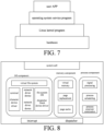
- FIG.7 shows a structural schematic diagram including a Linux operating system
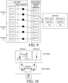
- FIG.8 shows a structural schematic diagram of a kernel of a Linux operating system.
- a complete Linux operating system mainly has four parts: hardware, Linux kernel program, operating system service program and user APP, wherein, user APP mainly refers to those word processing programs, Internet browser programs or APPs developed by users themselves (e.g., Taobao, Alipay, etc.); operating system service programs mainly refer to programs that provide services to users as part of the functions of the operating system, and on the Linux operating system, these programs include system programs such as shell command parsing and Linux kernel programming interface; the Linux kernel program is mainly configured for abstraction and access scheduling of hardware resources.
- Hardware includes but is not limited to CPU, memory, hard disk, memory device (or peripherals), etc.
- FIG.8 For the Linux kernel structure, it is shown as FIG.8 .
- the Linux kernel is a part resided in a hardware memory, and its main functions comprise I/O interaction, memory management and control of CPU access.
- FIG.8 also includes an interrupt and a scheduler, wherein the interrupt is the main way for the Linux operating system to interact with peripherals.
- the scheduler functions when an interrupt occurs.
- the low-level code stops the process which is running, saves its state in the kernel process structure, and starts the driver. Process scheduling also happens when the kernel completes some operations and starts a user process.
- the scheduler in FIG.8 comprises a dispatcher.
- scheduler in FIG.8 here is a dispatcher instead of scheduler, there is a difference between the two, both of scheduler and dispatcher are concepts related to scheduling of process (or thread), and the difference is that the scheduler will randomly select a process from several processes, while the dispatcher will assign a CPU to the process selected by the dispatcher.
- the Linux kernel is divided into three parts: I/O component, memory component and process component.
- the I/O component comprises all of the kernel parts that are responsible for interacting with peripherals and performing network and memory I/O operations.
- the I/O components include: highest-level virtual file system (VFS), which means that no matter whether a file comes from memory or disk (or other memory devices), the file is to be processed by the virtual file system first; underlying character device driver structure, block device driver structure and network driver structure, where the character device driver structure includes terminals (such as keyboards, printers, etc.) that transmit in units of characters and character device drivers (programs) that drives these terminals; the block device driver structure includes the file system, I/O dispatcher, and block (BLOCK) device driver (program); the network driver structure includes the Socket network protocol and network driver device.
- VFS virtual file system
- the I/O components includes: highest-level virtual file system (VFS), which means that no matter whether a file comes from memory or disk (or other memory devices), the file is to be processed by the virtual file system first; underlying character device driver structure, block device driver
- the mentioned file system is the system configured by Linux to specify files on memory devices (such as disks, NAND flash, etc.) or partitions, which provides a mapping conversion of a layer of files to the physical block layer of the memory device, i.e., a system for organizing files on the memory device.
- the mentioned I/O dispatcher may refer to a program or structure that performs some scheduling processing on the I/O requests provided by the file system.
- the main difference between the mentioned character device driver and block device driver is whether random access is allowed, wherein, the character device driver may not be accessed randomly, but may be read and written sequentially in units of byte streams; the block device driver may be accessed randomly in units of fixed-size blocks.
- the network driver device here is not an independent drive device, it is actually a character device, but the processing ways of the two are different.
- the socket network protocol may comprise, but not limited to: TCP/IP, UDP, etc.
- the memory component the program is loaded into the memory component and executed by the CPU.
- the process of loading the program virtual memory, page replacement and page cache, etc., will be involved.
- the process component is responsible for the creation, termination and scheduling of the process (i.e., the process of assigning the process to the corresponding CPU).
- the Linux kernel takes processes and threads as runnable entities, and adopts a unified scheduling strategy for scheduling.
- the top layer of the Linux kernel structure is a system calling interface, wherein all of system calls pass through this system calling interface.
- the system call passes the I/O request of the application running in the user mode to the Linux kernel running in the kernel mode, and after that, the Linux kernel calls the corresponding kernel function to complete the required processing, and return the processing result to the application.
- Linux is a multiprogramming system, and there are mutually independent processes running simultaneously on the Linux operating system. Each of processes independently owns various resources and runs independently. The Linux operating system achieves multitasking through running these processes in turn at short intervals, wherein, this short time interval is referred as a time slice.
- process scheduling the way of running processes in turn is referred as process scheduling, and the program that completes this process scheduling is referred as a scheduling program.
- Each of processes is exclusive to the processor 601 at runtime. Because the cost of switching between processes is high, and the creation speed is slow and consumed resource is large, the use of threads is generated.
- a process may include at least one thread.
- a thread may be an execution path of a process, and is the smallest unit of program execution, i.e., the basic unit of processor core scheduling.
- a thread do not monopolize any additional resources except for some resources for execution (such as program counter, register, and stack of a CPU cores, etc.), but each of threads in a same process shares all resources in the process.
- a thread may be divided into: User Level Thread (ULT) and Kernel Level Thread (KLT), where the dispatcher of the ULT is outside the Linux kernel; and the dispatcher of the KLT is inside the Linux kernel.
- the ULT may be a thread created through a thread library in the user space, and the creation, scheduling, destruction and communication of the thread are all completed in the user space.
- a Linux kernel is not aware of an ULT, nor does it directly schedule an ULT.
- the scheduling object of the Linux kernel is still a process. That is: the Linux kernel does not assign resources for ULT, and ULT only competes for resources in the same process. In this case, if a certain ULT is blocked in the Linux kernel, it will cause all other threads in the same process to be blocked, and the concurrency of the ULT to be limited.
- the KLT is created in the Linux kernel, and the Linux kernel may be aware and manipulate the KLT through the data structure included in the KLT, thereby, the Linux kernel may implement concurrency among ULTs in the same process through the KLT.
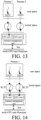
- FIG.9 shows the mapping relationship between ULT and KLT in the Linux operating system.
- a one-to-one mapping relationship is often employed between ULT and KLT, i.e., one ULT is mapped to one KLT, and the operation of the ULT may rely on the KLT, that is, the operating system dispatcher included in the Linux kernel assigns the KLT mapped with the ULT to the corresponding CPU core for running.
- the processing includes CPU core 0 and CPU core 1; three processes of process A, process B, and process C are created in user space, wherein, process A includes three user threads ULT1 to ULT3; process B includes two user threads ULT4 and ULT5; process C includes one user thread ULT6.
- one of the ULTs corresponds to one KLT, that is, ULT1 to ULT6 correspond to KLT1 to KLT6 respectively.
- the processor may simultaneously run two kernel threads mapped with user threads, e.g., run KLT2 on CPU core 0; run KLT3 on CPU core 1.
- the user space may refer to the space that may be operated by the user, e.g., both of the user APP and the operating system service program (layer) shown in FIG.7 above belong to the user space.
- the kernel space may refer to a space that may not be operated by the user, and is completed by the Linux kernel, e.g., the Linux kernel program (layer) shown in FIG.7 above belongs to the kernel space.
- the Linux kernel may be aware and manipulate KLT through the data structure included in the KLT, and the Linux kernel may further implement the concurrency among ULTs in the same process through the KLT.
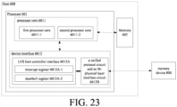
- FIG.10 shows an ULT calling relationship diagram without including KLT
- FIG.11 shows an ULT calling relationship diagram with including KLT.
- ULT1 of process 1 will send a data download request to the website through the network card, the network card is driven and managed by the operating system, Therefore, ULT1 issuing the data download request (GetData) may be completed by entering the Linux kernel with the help of a system call.
- GetData data download request
- the operating system will control the CPU to switch to process 2 instead of switching to ULT2 of process 1.
- ULT2 the information of the thread control block (TCB) corresponding to ULT is in the user space
- TLB thread control block
- KLT is created in the Linux kernel.
- Information of KLT such as TCB is created in the Linux kernel.
- the Linux kernel may be aware and manipulate KLT through these data structures to achieve concurrency among ULTs in the same process. That is to say, when there is no KLT, the Linux kernel may perform operations including switching among processes, as shown in FIG.10 . When there is a KLT, the Linux kernel may switch among ULTs in the same process, as shown in FIG.11 .
- the creation of KLT in the Linux kernel implements the concurrency among ULTs.
- a KLT is more suitable for a multi-CPU core processor than a process. In some examples, as shown in FIGs.12 to 14 .
- the present disclosure provides a host as shown in FIG.6 , which binds the first thread to the first CPU core to use a dedicated sending kernel thread to send I/O requests; binds the second thread to the second CPU core to use a dedicated receiving thread to receive I/O request feedback value to reduce the lock overhead required for shared global data usage.
- both of the first CPU core and the second CPU core may be included in the processor core 6011, i.e., the processor 601 shown in FIG.6 may be the first processor 201 described above, which may be a processor including multiple CPU cores.
- the first CPU core and the second CPU core may refer to two of the plurality of CPU cores described above, and the first CPU core may be any one of the plurality of CPU cores; the second CPU core may be any CPU core among the plurality of CPU cores other than the first CPU core.
- the first thread described here may be a sending kernel thread in the Linux kernel; the second thread described herein may be a receiving kernel thread in the Linux kernel.
- binding the first thread to the first CPU core means that the first CPU core is dedicated to processing the first thread, and the first thread is only assigned to run on the first CPU core, in other words, the first CPU core is only controlled by the first thread.
- binding the second thread to the second CPU core means that the second CPU core is dedicated to process the second thread, and the second thread is only assigned to run on the second CPU core.
- the I/O request may be generated by an application running on the processor, and the I/O request is converted by a device driver running on the processor into one or more request commands in a format supported by the memory device.
- the I/O request may be generated by the APP.
- the I/O request may be converted into one or more request commands in a format supported by the memory device and then sent to the memory device.
- the device driver may refer to the block device driver shown in FIG.8 .
- a Linux-based memory system is taken as an example for description.
- the Linux-based memory system includes: VFS layer, file system layer, Page Cache layer, general Block layer, I/O scheduling layer, Block device driver layer, and Block device layer.
- VFS layer file system layer
- Page Cache layer general Block layer
- I/O scheduling layer Block device driver layer
- Block device layer Block device layer
- the interaction process may be as follows: when the host initiates a random read and write of a data page, or a sequential read and write of a log file, the processor of the host will actually pass the I/O requests generated by the APP to the VFS layer of the Linux operating system.
- the function of the VFS layer is to perform I/O operations on the files in the selected directory according to the processor of the host, and pass the I/O request to the file system.
- the VFS layer is to determine the read and write I/O requests initiated for files under the selected directory (e.g., the selected directory is /AA1/AA2), and transfer the request to the corresponding file system (such as NFS), as shown in FIG. 16 .
- Page Cache which is a memory-based cache (cache layer of Page Cache), if data is found, reading and writing operation will be performed based on the memory cache, and if data is not found, it will continue to go to the next layer, at this point, the I/O request will be passed to the general Block layer, and the I/O request for the file will be converted into a Block I/O request at this layer, as shown in FIG. 17 .
- the Block I/O request After the I/O request is converted into a Block I/O request, the Block I/O request will be passed to the I/O scheduling layer, as shown in FIG.18 .
- the function of this layer is to rank a plurality of Block I/O requests and determine the order in which each of Block I/O requests is sent.
- the adopted scheduling algorithm may comprise a Completely Fair Scheduler (CFQ) algorithm or a deadline I/O scheduling algorithm.
- Block I/O request it will be decided which Block I/O request to be executed firstly and which Block I/O request to be executed later, at this point, the Block I/O request that may be executed will be passed to the Block device driver layer (on which device driver running), and finally the I/O request will be converted into one or more request commands through the Block device driver layer and sent to the real memory hardware (memory device), i.e., the Block device layer, as shown in FIG.19 .
- the Block device driver layer on which device driver running
- the I/O request will be converted into one or more request commands through the Block device driver layer and sent to the real memory hardware (memory device), i.e., the Block device layer, as shown in FIG.19 .
- the memory device completes the I/O read operation and write operation, it is either a write operation or a read operation, and at last returns the response through the above layers in reverse order, and finally, the host may obtain the result of this I/O read and write operation, as shown in FIG.20 .
- the I/O request may be, but is not limited to, referring to a read request, a data memory (or write) request, or a data drop request.
- the processor 601 further includes: a device interface 6012; the device interface includes: Host Controller Interface (HCI) 6012A; the host controller interface includes an interrupt register 6012A-1;
- HCI Host Controller Interface
- the host controller interface includes an interrupt register 6012A-1;
- the second CPU core 6011-2 is further configured to: in response to the control of the second thread, poll the interrupt register to receive the feedback information.
- the second CPU core 6011-2 is configured to: in response to the control of the second thread, periodically access the interrupt register at a preset time interval to determine whether the feedback information is received in the interrupt register; if the feedback information is received, obtain the feedback information from the interrupt register.
- the foregoing description relates to some operations of the second CPU core when the second thread runs.
- the second CPU core polls the interrupt register included in the HCI in response to the control of the second thread, so as to receive the aforementioned feedback information related to the I/O request.
- the feedback information may refer to returned data as shown in FIG.20 .
- the process of polling the interrupt register by the second CPU core in response to the control of the second thread may include the second CPU core periodically accesses the interrupt register at a preset time interval.
- the preset time interval may be set according to actual conditions.
- the present disclosure adopts a polling strategy for receiving feedback information, so that the entire process of receiving feedback information may be processed in one thread, which compared with the interrupt handling mechanism, eliminates a large amount of overhead caused by interrupt context switching in the interrupt handling mechanism.
- the host 60 further includes a memory 602; the memory 602 is configured to store a request command queue; the request command queue includes: one or more request commands; the one or more request commands correspond to one or more I/O requests;
- the first CPU core 6011-1 is configured to: in response to the control of the first thread, obtain the one or more request commands from the request command queue, and send the one or more request commands to the memory device.
- request command queue may be a sequential queue or a linked list queue, where the sequential queue adopts the first-in-first-out constraint; and the linked list queue may adopt the first-in-first-out constraint, and may also adopt other constraints, such as first-in-last-out, etc.
- the present disclosure only illustrates the function of the request command queue and how to use it by taking the queue with the first-in-first-out constraint as an example. That is, the first CPU core 6011-1 obtains the request commands from the memory according to the sequence in which the request commands are stored, and sends the request commands.
- the memory 602 may be the same as the aforementioned memory 304, which may include program memory, data memory, write buffer/cache, read buffer/cache, data buffer/cache, and mapping buffer/cache for storing write data and read data.
- the memory 602 may be implemented with a volatile memory.
- the memory 602 may be implemented with Static Random Access Memory (SRAM), Dynamic Random Access Memory (DRAM), or both.
- the host controller interface 6012A further includes: a doorbell register 6012A-2; the second CPU core 6011-2 is further configured to: access the doorbell register to determine the I/O request corresponding to the feedback information.
- the first CPU core is further configured to: access the doorbell register, and assign a transmission channel required for the I/O request in a ready state.
- the doorbell register is also referred as a Doorbell register.
- the Doorbell register provides a request command distribution channel for a plurality of CPU cores (including the transmission channel of the request command from the host side to the memory device side), and each of CPU cores may send request commands to the memory device through the Doorbell register or receive the feedback information of the request command through the Doorbell register and determine the I/O request corresponding to the received feedback information. That is to say, both of the first CPU core and the second CPU core are to access the Doorbell register to obtain the transmission channel of the data or obtain the source of the data.
- the access mode for the doorbell register includes a locked access mode, wherein the locked access mode includes that the doorbell register is only accessed by the first CPU core or the second CPU core at a same time.
- the Doorbell register is only accessed by the first CPU core or the second CPU core at the same time.
- the first CPU core when the first CPU core sends a request command through the Doorbell register, the Doorbell register will be locked, and at this point, the second CPU core may not be able to access the Doorbell register.
- the Doorbell register may include 32 bits, and each of bits represents a distribution channel for the host to send an I/O request to the memory device.
- the bit corresponding to the used distribution channel in the Doorbell register will be set to 1, and the rest of the bits will remain as 0.
- the first CPU core described in this disclosure accesses the doorbell register, and the process of assigning the transmission channel required for the I/O request in the ready state may be as follows: the first CPU core firstly traverses the 32 distribution channels (also transmission channels) included in the Doorbell register and from which determines a distribution channel that is not occupied by other CPU cores, wherein, the flag bit related to the unoccupied distribution channel may be 0; the flag related to the occupied distribution channel may be 1.
- the first CPU core sets the identification bit of the selected unoccupied distribution channel from 0 to 1, thereby indicates that the distribution channel is occupied.
- the first CPU core sends the request command to the memory device through the distribution channel. After finishing sending the request command, the first CPU core unlocks the Doorbell register, so that other CPU cores (such as the second CPU core) may also access the Doorbell register.
- the process described in this disclosure that the second CPU core 6011-2 accesses the doorbell register to determine the I/O request corresponding to the feedback information may be as follows: reading the current value of the Doorbell register and comparing it with the uncompleted command list previously issued by the host, wherein, since each of bits in the Doorbell register being 0 means that the request command has been completed, each of bits in the Doorbell register being 1 means that the request command has not been completed. Since the Doorbell register is accessed with a lock, only one bit in the Doorbell register is 1 each time a request command is sent, thus the I/O request corresponding to the feedback information may be determined.
- the device interface further includes: a unified protocol circuit and an M-physical layer interface circuit 6012B, wherein; the unified protocol circuit and the M-physical layer interface circuit are coupled with the host controller interface and configured to: send a request command to the memory device or receive the feedback information sent by the memory device, wherein the request command is generated based on the I/O request.
- the mentioned Unified Protocol (UniPro) circuit and M-physical layer (M-PHY) circuit 6012B may be the host-side UFS Inter Connect (UIC) layer, which is an interface through which the host is directly connected to the memory device.
- UFS Inter Connect UFS Inter Connect
- the implementation of the UniPro circuit and the M-PHY circuit may refer to the UniPro protocol and the M-PHY protocol, which will not be repeated here.
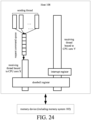
- FIG.24 shows a schematic flowchart of a host sending an I/O request to a memory device and receiving feedback information, as provided in an example of the present disclosure.
- the sending thread is bound to CPU core X and the receiving thread is bound to CPU core Y.
- the request command may be obtained from the request command queue stored in the memory in a first-in first-out manner by the sending thread on the CPU core X, and the obtained request command is sent to the memory device.
- the interrupt register When the host receives the feedback information sent by the memory device, the interrupt register may be accessed in a polling manner by the receiving thread on the CPU core Y, and the feedback information may be processed when the interrupt register receives the feedback information. That is, processing the I/O requests between the host and the memory device with two dedicated CPU cores reduces a large amount of lock overhead.
- an example of the present disclosure also provides an information processing method for a host, as shown in FIG.25 , the method may include:
- controlling the second CPU core to receive the feedback information which is related to the I/O request and sent by the memory device further includes: when the second thread runs, controlling the second CPU core to poll an interrupt register included in the host to receive the feedback information.
- controlling the second CPU core to poll an interrupt register included in the host to receive the feedback information includes: periodically accessing the interrupt register at a preset time interval to determine whether the feedback information is received in the interrupt register; if the feedback information is received, obtaining the feedback information from the interrupt register.
- controlling the first CPU core to send an input/output (I/O) request to a memory device coupled to the host includes:
- the method further includes:
- the access mode for the doorbell register includes a locked access mode, wherein the locked access mode includes that the doorbell register is only accessed by the first CPU core or the second CPU core at a same time.
- An example of the present disclosure also provides an electronic system 2600, as shown in FIG.26 , the electronic system may include:
- the processor further includes: a device interface; the device interface includes a host controller interface; the host controller interface includes an interrupt register;
- the host further includes a memory; the memory is configured to store a request command queue; the request command queue includes: one or more request commands; the one or more request commands correspond to one or more I/O requests;
- the "first" and “second” in the first access command and the second access command here are only for the purpose of easily describing access commands in different processes, and are not used for quantitative limitation. That is: the first access command is an access command sent by the second CPU core when accessing the interrupt register; the second access command is an access command sent by the first CPU core when accessing the memory.
- An electronic system provided by an example of the present disclosure includes the host provided above, and the description of the host may refer to the foregoing description of the host for, which will not be repeated here.
- the memory device includes a memory system as shown in FIGs. 1 to 5 above, which will not be repeated here.
- An example of the present disclosure also provides a computer-readable memory medium, wherein a computer program is stored thereon, and when executed by a processor, the computer program implements operations of the method according to any one of the foregoing.
- the aforementioned memory media include: various media capable of storing program codes such as removable memory devices, Read-Only Memory (ROM), Random Access Memory (RAM), magnetic disk or optical disk, etc.
- the disclosed devices and methods may be implemented in other ways.
- the device examples described above are only illustrative, e.g., the division of the elements is only a logical function division, and in actual implementation, there may be other division methods, such as a plurality of elements or components may be combined, or may be integrated into another system, or some features may be ignored, or not implemented.
- the coupling, or direct coupling, or communication connection between the components shown or discussed may be indirect coupling or communication connection of devices or elements through some interfaces, and may be electrical, mechanical or in other forms.
- the elements described above as separate parts may or may not be physically separated, and the parts displayed as elements may or may not be physical elements, i.e., they may be located in one place or distributed to a plurality of network elements; and portions or all of these elements may be selected according to actual needs to achieve the purpose of the solution of this example.
- each functional unit in each example of the present disclosure may be integrated into one processing unit, or each unit may be used as a single unit, or two or more units may be integrated into one unit; the integrated units described above may be implemented in the form of hardware, or in the form of hardware plus software functional units.
- the above-mentioned integrated units of the present disclosure are implemented in the form of software function modules and sold or used as independent products, they may also be stored in a computer-readable memory medium.
- the essence of technical solutions of the examples of the present disclosure or the part that contributes to the prior art may be embodied in the form of a software product, which is stored in a memory medium, and includes several instructions to enable a computer device (which may be a personal computer, server, or network device, etc.) to execute all or part of the methods described in various examples of the present disclosure.
- the aforementioned memory media include: various media capable of storing program codes such as removable memory devices, ROM, RAM, magnetic disk or optical disk, etc.
Landscapes
- Engineering & Computer Science (AREA)
- Theoretical Computer Science (AREA)
- Physics & Mathematics (AREA)
- General Engineering & Computer Science (AREA)
- General Physics & Mathematics (AREA)
- Software Systems (AREA)
- Human Computer Interaction (AREA)
- Computer Hardware Design (AREA)
- Advance Control (AREA)
Abstract
Description
- The disclosure relates to a technical field of memory, and in particular to a host, an information processing method, an electronic system, and a readable memory medium.
- At present, an electronic system may include a host and a memory device including a memory system, wherein a Central Processing Unit (CPU) core included in the host may send data to the memory device or receive feedback from the memory device. At present, the data transmission mode adopted by the CPU core requires a large amount of lock protection, which results in a large lock overhead for the electronic system; and the feedback reception mode adopted by the CPU core requires the use of interrupt context switching, which takes a lot of time to save and restore data, as a result, the time overhead of the electronic system is relatively large, therefore causing poor operation performance of the host in the electronic system for the memory device.
- In view of this, the present disclosure provides a host, an information processing method, an electronic system, and a readable memory medium.
- In a first aspect, the present disclosure provides a host, including: a first central processing unit (CPU) core bound with a first thread and a second CPU core bound with a second thread; wherein,
- the first CPU core is configured to: in response to control of the first thread, send an input/output (I/O) request to a memory device coupled to the host;
- the second CPU core is configured to: in response to the control of the second thread, receive feedback information which is related to the I/O request and sent by the memory device.
- In the scheme described above, wherein the processor further includes: a device interface; the device interface includes: a host controller interface; the host controller interface includes an interrupt register;
the second CPU core is further configured to: in response to the control of the second thread, poll the interrupt register to receive the feedback information. - In the scheme described above, wherein, in some examples, the second CPU core is configured to: in response to the control of the second thread, periodically access the interrupt register at a preset time interval to determine whether the feedback information is received in the interrupt register; if the feedback information is received, obtain the feedback information from the interrupt register.
- In the scheme described above, wherein the host further includes a memory; the memory is configured to store a request command queue; the request command queue includes: one or more request commands; the one or more request commands correspond to one or more I/O requests;
the first CPU core is configured to: in response to the control of the first thread, obtain the one or more request commands from the request command queue, and send the one or more request commands to the memory device. - In the scheme described above, wherein the host controller interface further includes: a doorbell register;
the second CPU core is further configured to: access the doorbell register to determine the I/O request corresponding to the feedback information. - In the scheme described above, wherein the first CPU core is further configured to: access the doorbell register, and assign a transmission channel required for the I/O request in a ready state.
- In the scheme described above, wherein the access mode for the doorbell register includes a locked access mode, wherein the locked access mode includes that the doorbell register is only accessed by the first CPU core or the second CPU core at a same time.
- In the scheme described above, wherein the I/O request is generated by an application running on the processor, and the I/O request is converted by a device driver running on the processor into one or more request commands in a format supported by the memory device.
- In the scheme described above, wherein the device interface further includes: a unified protocol circuit and an M-physical layer interface circuit, wherein;
the unified protocol circuit and the M-physical layer interface circuit are coupled with the host controller interface and configured to: send a request command to the memory device or receive the feedback information sent by the memory device, wherein the request command is generated based on the I/O request. - In the scheme described above, wherein the memory device comprises a Universal Flash Memory (UFS) device.
- In the scheme described above, wherein the operating system running on the host comprises a Linux operating system.
- In the scheme described above, wherein the processor includes a plurality of CPU cores, wherein, a first CPU core is any one of the plurality of CPU cores; a second CPU core is any one of the plurality of CPU cores other than the first CPU core.
- In a second aspect, the present disclosure further provides an information processing method for a host, including:
- binding a first thread to a first central processing unit (CPU) core included in the host;
- binding a second thread to a second CPU core included in the host;
- wherein, when the first thread runs, controlling the first CPU core to send an input/output (I/O) request to the memory device coupled to the host; and when the second thread runs, controlling the second CPU core to receive feedback information which is related to the I/O request and sent by the memory device.
- In the scheme described above, wherein when the second thread runs, controlling the second CPU core to receive the feedback information which is related to the I/O request and sent by the memory device, further includes:
when the second thread runs, controlling the second CPU core to poll an interrupt register included in the host to receive the feedback information. - In the scheme described above, wherein the controlling the second CPU core to poll an interrupt register included in the host to receive the feedback information includes: periodically accessing the interrupt register at a preset time interval to determine whether the feedback information is received in the interrupt register; if the feedback information is received, obtaining the feedback information from the interrupt register.
- In the scheme described above, wherein when the first thread runs, controlling the first CPU core to send an input/output (I/O) request to a memory device coupled to the host, includes:
- when the first thread runs, controlling the first CPU core to obtain one or more request commands from a request command queue stored in the memory of the host, and sending the one or more request commands to the memory device;
- wherein, the one or more request commands correspond to one or more I/O requests.
- In the scheme described above, wherein the method further includes:
- when the first thread runs, controlling the first CPU core to access the doorbell register included in the host, and assigning a transmission channel required for the I/O request in a ready state;
- when the second thread runs, controlling the second CPU core to access the doorbell register to determine the I/O request corresponding to the feedback information.
- In the scheme described above, wherein the access mode for the doorbell register includes a locked access mode, wherein the locked access mode includes that the doorbell register is only accessed by the first CPU core or the second CPU core at a same time.
- In a third aspect, the present disclosure relates to an electronic system, including:
- a host; the host includes a processor; the processor is configured to: bind a first thread to a first central processing unit (CPU) core included in the processor; bind a second thread to a second CPU core included in the processor; run the first thread, such that the first CPU core is controlled to send an input/output (I/O) request to a memory device;
- and a memory device coupled to the host; the memory device is configured to: receive and process the I/O request; generate feedback information related to the I/O request; send the feedback information to the host;
- the processor is further configured to: run the second thread, such that the second CPU core is controlled to receive the feedback information sent by the memory device.
- In the scheme described above, wherein the processor further includes: a device interface; the device interface includes a host controller interface; the host controller interface includes an interrupt register;
- the second CPU core is further configured to: in response to the control of the second thread, periodically send a first access command to the interrupt register at a preset time interval;
- the interrupt register is configured to: in response to the first access command, when receiving the feedback information sent by the memory device, send the feedback information to the second CPU core.
- In the scheme described above, the host further includes a memory; the memory is configured to store a request command queue which includes one or more request commands corresponding to one or more I/O requests;
- the first CPU core is further configured to: in response to the control of the first thread, send a second access command to the memory;
- the memory is configured to: in response to the second access command, obtain the one or more request commands from the request command queue, and send the one or more request commands to the first CPU core;
- the first CPU core is further configured to: send the one or more request commands to the memory device.
- In a fourth aspect, the present disclosure also provides a computer-readable memory medium having a computer program stored thereon, which executed by a processor, implements the method according to any one of the foregoing aspects.
- Examples of the present disclosure provide a host, an information processing method, an electronic system, and a readable memory medium. Wherein the host includes: a first central processing unit (CPU) core bound with a first thread and a second CPU core bound with a second thread; wherein, the first CPU core is configured to: in response to control of the first thread, send an input/output (I/O) request to a memory device coupled to the host; the second CPU core is configured to: in response to the control of the second thread, receive feedback information which is related to the I/O request and sent by the memory device. The host provided in an example of the present disclosure, by binding the first thread to the first CPU core and the second thread to the second CPU core, and processing the I/O requests between the host and the memory device with two application-specific CPU cores, reduces a large amount of lock overhead.
- In the accompanying drawings, which are not necessarily drawn to scale, like reference numerals may describe similar components in the different views of drawings. The same numbers with different letter suffixes may represent different instances of a similar component. The accompanying drawings illustrate, by way of example and not limitation, various examples discussed in this document.
-
FIG.1 shows a system block diagram of an example electronic device comprising a memory system; -
FIG.2 shows a structural example diagram of a host in the system shown inFIG.1 ; -
FIG.3 shows a structural schematic diagram of a memory controller included in the memory system in the system shown inFIG.1 ; -
FIG.4 shows a structural schematic diagram of a memory device included in a memory system; -
FIG.5 shows a schematic diagram of the processing flow of the host sending an I/O request to the memory device and receiving feedback for the I/O request from the memory device; -
FIG.6 shows a first structural schematic diagram of a host provided by an example of the present disclosure; -
FIG.7 shows a schematic diagram of the logical structure of a Linux-based operating system provided in an example of the present disclosure; -
FIG.8 shows a schematic diagram of the structure of the Linux kernel provided in an example of the present disclosure; -
FIG.9 shows a schematic diagram of a mapping relationship between a user thread and a kernel thread in an example of the present disclosure; -
FIG.10 shows a schematic diagram of scheduling between processes when a user thread is not mapped to a kernel thread provided by an example of the present disclosure; -
FIG.11 shows a schematic diagram of scheduling between threads when a user thread is mapped to a kernel thread provided by an example of the present disclosure; -
FIG.12 shows a schematic diagram of scheduling of threads in a same process running on a same CPU core provided by an example of the present disclosure; -
FIG.13 shows a schematic diagram of scheduling of different processes running on different CPU cores provided by an example of the present disclosure; -
FIG.14 shows a schematic diagram of scheduling of threads in a same process running on different CPU cores provided by an example of the present disclosure; -
FIG.15 shows a structural schematic diagram of a Linux-based memory system provided by an example of the present disclosure; -
FIGs. 16-20 show the interactive relationship between layers in the Linux-based memory system provided by the examples of the present disclosure; -
FIG.21 shows a second structural schematic diagram of a host provided by an example of the present disclosure; -
FIG.22 shows a third structural schematic diagram of a host provided by an example of the present disclosure; -
FIG.23 shows a fourth structural schematic diagram of a host provided by an example of the present disclosure; -
FIG.24 shows a schematic flowchart of a host sending an I/O request to a memory device and receiving feedback information provided by an example of the present disclosure; -
FIG.25 shows a schematic flowchart of an information processing method for a host provided by an example of the present disclosure; -
FIG.26 shows a structural schematic diagram of an electronic system provided by an example of the present disclosure. - Various examples of the present disclosure are described in more detail below with reference to the accompanying drawings. Other examples that are variations of any disclosed example may be formed by differently configuring or arranging elements and features of the disclosed examples. Therefore, examples of the present disclosure are not limited to the examples set forth herein. Rather, the described examples are provided so that the disclosed examples will be thorough and complete, and will fully convey the scope of the disclosed examples to those skilled in the art to which the disclosed examples belong. It is to be noted that references to "an example," "another example," etc., do not necessarily refer to only one example, and that different references to any such phrase are not necessarily to the same example. It should be understood that although the terms "first," "second," "third," etc., may be herein to identify various elements, these elements should not be limited by these terms. These terms are to distinguish one element from another element having the same or similar name. Therefore, a first element in an example may also be referred as a second element or third element in another example without departing from the spirit and scope of the examples of the present disclosure.
- The drawings are not necessarily drawn to scale, and in some instances the scale may have been exaggerated to clearly illustrate features of the examples. When an element is referred as being connected or coupled to another element, it should be understood that the former may be directly connected or coupled to the latter or electrically connected or coupled to the latter via one or more intervening elements therebetween. In addition, it should also be understood that when an element is referred as being "between" two elements, it may be the only element between the two elements, or one or more intervening elements may also be present.
- The terminology herein is for the purpose of describing particular examples only and is not intended to be limiting of the present disclosure. As described herein, singular forms are intended to include plural forms unless the context clearly dictates otherwise. Unless otherwise stated or clearly understood as a singular form from the context, the articles "a" and/or "an" described in the examples of the present disclosure and the appended claims shall be collectively interpreted as meaning "one or more". It should be further understood that the terms "include", "comprising", "include" and "including" described in the examples of the present disclosure specify the presence of stated elements and do not exclude the presence or addition of one or more other elements. The term "and/or" described in the examples of the present disclosure includes any and all combinations of one or more of the associated listed items. Unless otherwise defined, all terms including technical and scientific terms described in the examples of the present disclosure have the same meanings as commonly understood by one of ordinary skill in the art to which the present disclosure belongs in view of the examples of the present disclosure. It should be further understood that, unless clearly defined by the examples of the present disclosure, terms such as those defined in commonly described dictionaries should be interpreted as having meanings consistent with their meanings in the context of the examples of the present disclosure and related technologies, and should not be interpreted in an idealized or overly formal way.
- In the following description, numerous specific details are set forth in order to provide a thorough understanding of the disclosure, and the disclosure may be practiced without some or all of these specific details. In other instances, well known processing structures and/or processes are not described in detail so as not to unnecessarily obscure the present disclosure. It should also be understood that in some cases, unless stated otherwise, it will be apparent to a person skilled in the relevant art that features or elements described with respect to one example may be used alone or in combination with other features or elements of another example. Hereinafter, various examples of the present disclosure are described in detail with reference to the accompanying drawings. The following description focuses on details to facilitate understanding of examples of the present disclosure. Well-known technical details may be omitted so as not to obscure the features and aspects of the examples of the disclosure.
- Examples of the present disclosure will be further described in detail below in conjunction with the accompanying drawings and specific examples.
-
FIG.1 shows a system block diagram of an example electronic device comprising a memory system. InFIG.1 , the electronic device may be a mobile phone, a desktop computer, a laptop computer, a tablet, a vehicle computer, a gaming console, a printer, a positioning device, a wearable electronic device, a smart sensor, a Virtual Reality (VR) device, an Augmented Reality (AR) device, or any other suitable electronic devices having memory system therein. As shown inFIG.1 ,system 100 is a system in an electronic device, which may include ahost 108 and amemory system 102, and the memory system is included in a memory device; wherein, - In some examples, as shown in
FIG.2 , thehost 108 may include afirst processor 201 such as a Central Processing Unit (CPU) or a System of Chip (SoC), where the system on a chip may, e.g., be an Application Processor (AP). Thefirst processor 201 may include amulti-core processor 2011 and a peripheral interface (or referred as a device interface) 2012, wherein themulti-core processor 2011 may include a plurality of CPU cores (CPU core 2011-1 to CPU core 2011- N, where N is an integer greater than 1), where each of the CPU cores may include logic circuits (or modules) with logic operation and control capabilities. Theperipheral interface 2012 is a channel for communicating with the memory system, so as to realize the function of the host reading data from the memory system or writing data into the memory system by the host. - The
host 108 also includes at least one operating system (OS) that may manage and control the functions and operations performed in thehost 108. The OS may enable interoperability between ahost 108 coupled to thememory system 102 and users who need and use thememory system 102. The OS may support functions and operations corresponding to the request of the user, for example instead of limitation, depending on whether the type of thehost 102 is a removable host, the OS may be classified into a general-purpose operating system and a mobile operating system, wherein the general-purpose operating system may include a personal operating system and an enterprise operating system, and the personal operating system may comprise operating systems configured to support services for general purposes, including Windows and Chrome; and the enterprise operating system may comprise an operating system dedicated to ensuring and supporting higher performance, including Windows server, Linux, and Unix. The mobile operating system may refer to an operating system for mobility services or functions (e.g., a power saving function), and the mobile operating system may comprise an operating system such as Android, I/OS, and Windows Mobile, etc. In some examples, thehost 108 may include a plurality of OSs; accordingly, thehost 108 may run a plurality of operating systems related to thememory system 102. In some other examples, thehost 108 converts the request of the user into one or more commands, and transmits the one or more commands to thememory system 102, so that thememory system 102 performs operations associated with the one or more commands. It should be known that the OS is configured in the CPU core, e.g., a mobile electronic device including UFS may be applied in the android platform, and the CPU core included in the mobile electronic device uses Linux. - The
memory system 102 is capable of operating or performing a specific function or performing internal various operations in response to a request from thehost 108. In some examples,memory system 102 is capable of storing data accessed byhost 108.Memory system 102 may act as a primary memory system or a secondary memory system forhost 108. Thememory system 102 and thehost 108 may be electrically connected and communicate according to corresponding protocols. Thememory system 102 may be implemented and packaged into different types of terminal electronic products, including, for example instead of limitation: Solid State Drives (SSD), Multimedia Cards (MMC), Embedded MMC (eMMC), Reduced Size MMC (RSMMC), Micro MMC, Secure Digital (SD) cards, Mini SD, Micro SD, Universal Serial Bus (USB) memory devices, Universal Flash Memory (UFS) devices, Compact Flash (CF) cards, Smart Media (SM) cards and memory sticks, etc. - In some examples,
memory system 102 may also be configured as part of devices, e.g., a computer, Ultra Mobile PC (UMPC), workstation, netbook, Personal Digital Assistant (PDA), portable computer, web tablet, tablet computer, wireless telephone, mobile phone, smart phone, e-book, portable multimedia players (PMP), portable game console, navigation system, black box, digital camera, Digital Multimedia Broadcasting (DMB) player, three-dimensional (3D) TV, smart TV, digital audio recorder, digital audio player, digital picture recorder, digital picture player, digital video recorder, digital video player, a memory device for configuring a data center, a device capable of transmitting and receiving information in a wireless environment, one of various electronic devices for configuring a home network, one of various electronic devices for configuring a computer network, one of various electronic devices for configuring a telematics network, a Radio Frequency Identification (RFID) device, or one of various components for configuring a computing system. - Referring back to
FIG. 1 , thememory system 102 may have one ormore memory devices 104 and amemory controller 106. Thememory controller 106 may respond to the request of thehost 108, and in turn control thememory device 104, e.g., thememory controller 106 may read data from thememory device 104, and transmit the read data to thehost 108; thememory controller 106 may also receive data to be stored from thehost 108, and store the data to be stored into thememory device 104. That is, thememory controller 106 is capable of controlling write (or program) operation, read operation, erase operation, background operation, etc., of thememory device 104. - In some examples, as shown in
FIG.3 , thememory controller 106 may include a front-end interface 301, a back-end interface 302, aprocessor 303, and amemory 304, wherein the above-mentionedcomponents memory controller 106 may share transmission signals inside thememory controller 106 through an internal bus. In some examples, the front-end interface 301 may interface thehost 108 with thememory system 102 in response to the protocol of thehost 108, and the front-end interface 301 exchanges transmission commands and data operations between thehost 108 and thememory system 102. The front-end interface 301 may process commands and data sent by thehost 108, and may include at least one of Universal Serial Bus (USB), MultiMedia Card (MMC), Peripheral Component Interconnect Express (PCI-e or PCIe), Small Computer System Interface (SCSI), Serial SCSI (SAS), Serial Advanced Technology Attachment (SATA), Parallel Advanced Technology Attachment (PATA), Small Computer System Interface (SCSI), Enhanced Small Disk Interface (ESDI), and Integrated Drive Electronics (IDE). In some examples, the front-end interface 301 is a component in thememory system 102 for exchanging data with thehost 108 and may be implemented by firmware which is referred as Host Interface Layer (HIL). - Back-
end interface 302 may be an interface for commands and data transferred betweenmemory controller 106 andmemory device 104, allowingmemory controller 106 to controlmemory device 104 in response to requests communicated fromhost 108. The back-end interface 302 may generate control signals for controlling thememory device 104. In some examples, if thememory device 104 is a NAND flash memory, the back-end interface 302 may write data into thememory device 104 or read data from thememory device 104 under the control of thesecond processor 303. The back-end interface 302 may process commands and data between thememory controller 106 and thememory device 104, e.g., operations of a NAND flash interface, especially operations between thememory controller 106 and thememory device 104. According to an example, the back-end interface 302 may be implemented as a component for exchanging data with thememory device 104 through firmware referred as Flash Interface Layer (FIL). - The
second processor 303 may be implemented by a microprocessor or a central processing unit (CPU). Thememory system 102 may include one or moresecond processors 303. Thesecond processor 303 may control all the operations of thememory system 102. By way of example and not limitation, thesecond processor 303 may control a program operation or a read operation of thememory device 104 in response to a write request or a read request from thehost 108. According to an example, thesecond processor 303 may use or run firmware to control all of the operations of thememory system 102. In this disclosure, firmware may be referred as a Flash Translation Layer (FTL). The FTL may operate as an interface between thehost 108 and thememory device 104. Thehost 108 may transmit requests related to write operations and read operations to thememory device 104 through the FTL. For example, thememory controller 106 uses thesecond processor 303 when performing an operation requested from thehost 108 in thememory device 104. Asecond processor 303 coupled to thememory device 104 may process instructions or commands related to commands from thehost 108. Thememory controller 106 may perform a foreground operation such as a command operation corresponding to a command input from thehost 108, e.g., a program operation corresponding to a write command, a read operation corresponding to a read command, and an erase/drop operation corresponds to an erase/drop command, and a parameter set operation corresponds to a set parameter command or a set feature command with a set command. - For another example, the
memory controller 106 may perform background operations on thememory device 104 through thesecond processor 303. By way of example instead of limitation, these background operations may include Garbage Collection (GC) operation, Wear Leveling (WL) operation, mapping clear operation, and bad block management operation that checks or searches for bad blocks. The garbage collection operation may include an operation of copying and processing data stored in a certain memory block in the memory device 104 (the memory device shown inFIG.4 ) to another memory block. The wear leveling operation may include an operation of exchanging and processing stored data among memory blocks MEMORY BLOCK<0, 1, 2,... > of thememory device 104. The mapping clear operation may include an operation of storing mapping data stored in thememory controller 106 into memory blocks MEMORYBLOCK<0, 1, 2,... > of thememory device 104. The bad block management operation may include an operation of checking and processing bad blocks in memory blocks MEMORY BLOCK<0, 1, 2,... > of thememory device 104. Thememory controller 106 may respond to an operation of accessing memory blocks MEMORY BLOCK<0, 1, 2,... > of thememory device 104, wherein the operation of accessing memory blocks MEMORY BLOCK<0, 1, 2,... > of thememory device 104 may include performing a foreground operation or background operation on memory blocks MEMORY BLOCK<0, 1, 2,... > of thememory device 104. - The
memory 304 may comprise a working memory of thememory controller 106, configured to store data for driving thememory controller 106. In some examples, when thememory controller 106 controls thememory device 104 in response to a request from thehost 108, thememory 304 may store firmware driven by thesecond processor 303 and data (e.g., metadata) required to drive the firmware.Memory 304 may also comprise a buffer ofmemory controller 106, configured to temporarily store write data transferred fromhost 108 intomemory device 104 and read data transferred frommemory device 104 to host 108.Memory 304 may include program memory, data memory, write buffer/cache, read buffer/cache, data buffer/cache, and mapping buffer/cache for storing write data and read data.Memory 304 may be implemented by volatile memory.Memory 304 may be implemented by Static Random Access Memory (SRAM), Dynamic Random Access Memory (DRAM), or both. - Although
FIG.3 showsmemory 304 being included inmemory controller 106, the present disclosure is not limited thereto. In an implementation, thememory 304 may be included external to thememory controller 106, and thememory controller 106 may input and output data to and from thememory 304 through a separate memory interface (not shown). - Referring back to
FIG. 1 ,memory device 104 may comprise a non-volatile memory device that may retain data stored therein even when it is not supplied with power. Thememory device 104 may store data provided from thehost 108 through a write operation; thememory device 104 may also provide the stored data to thehost 108 through a read operation. In an example of the present disclosure,memory device 104 may be any memory disclosed, e.g., a volatile memory device such as dynamic random access memory (DRAM) and static RAM (SRAM), or a non-volatile memory device such as read-only memory (ROM), Mask ROM (MROM), Programmable ROM (PROM), Erasable and Programmable ROM (EPROM), Electrically Erasable and Programmable ROM (EEPROM), Ferroelectric RAM (FRAM), Phase Change RAM (PRAM), Magnetoresistive RAM (MRAM), Resistive RAM (RRAM or ReRAM) and Flash memory (e.g. 3D NAND Flash). - As shown in
FIG.4 , thememory device 104 may include a plurality of memory blocks MEMORY BLOCK<0, 1, 2,... >. Each of memory blocks may include a plurality of pages P<0, 1, 2, 3, 4,... >. Also, although not shown in the drawings, each of the pages P<0, 1, 2, 3, 4,... > may include a plurality of memory cells. Wherein, according to the number of bits that may be stored or represented in a single memory cell, memory cells are classified into any one of different types of memory blocks such as Single Level Cell (SLC) memory blocks and Mutil Level Cell (MLC) memory blocks. Here, the SLC memory block includes a plurality of pages implemented by memory cells each storing one bit of data. A SLC memory block may have high performance of data I/O operation and high endurance. A MLC memory block includes a plurality of pages implemented by memory cells each storing a plurality of bits of data (e.g., two or more bits). Compared with a SLC memory block, a MLC memory block may have larger memory capacity for a same space. In terms of memory capacity, MLC memory blocks may be highly integrated. In an example, thememory device 104 may be implemented with a memory block such as a Double Level Cell (DLC) memory block, a Trinary Level Cell (TLC) memory block, a Quad Level Cell (QLC) memory block or memory block composed of the types of level cell described above. A MLC memory block may include a plurality of pages implemented by memory cells each capable of storing 2 bits of data. A Trinary Level Cell (TLC) memory block may include a plurality of pages implemented by memory cells each capable of storing 3 bits of data. A Quad Level Cell (QLC) memory block may include a plurality of pages implemented by memory cells each capable of storing 4 bits of data. In other examples, thememory device 104 may include memory blocks composed of memory cells each capable of storing 5 or more bits of data. - Based on the foregoing example electronic device system comprising a memory system, as shown in
FIG.5 , a schematic diagram of interaction between a host and a memory system is showed. InFIG.5 , two processes are included: the process of the host sending an Input/Output (I/O) request to the memory system through a sending thread (i.e., a sending kernel thread) and the process of the host receiving data related to the I/O request fed back by the memory system to the host through the receiving thread (i.e., the receiving kernel thread), wherein, in the former process, the host employs a plurality of sending kernel threads to send I/O requests to the memory system through doorbell registers, each of sending kernel threads requires a large amount of lock protection to protect shared data at runtime, which causes a large amount of lock overhead and takes a large amount of time in the locking and unlocking process, therefore the efficiency of accessing the memory system is not high. In the latter process, the host receives data related to the I/O request fed back by the memory system through the interrupt register and the doorbell register, in this process, the interrupt mechanism employed by the operating system of the host is implemented by the way of interrupting context switching, this receiving method takes a large amount of time to process operations such as saving and restoring registers and memory page tables, updating kernel-related data structures, etc., therefore causing a large system overhead. Since when the operating system of the host manages the peripherals (including memory system, e.g., memory devices) connected to the host, due to the speed of the peripheral is much lower than the operating speed of the first processor of the host, it is impossible for the first processor of the host to monitor the status of the peripherals all the time, thus an interrupt mechanism is introduced. The interrupt mechanism may be understood according to the following description: when a peripheral is to process a peripheral-related event (reading or writing) in the operating system, the peripheral may actively notify the operating system, i.e., interrupt the normal execution between the operating system and the application (APP) included in the host, to complete the peripheral-related processing, and then resume the normal execution between the operating system and the APP. In the interrupt process described above, interrupt context switching is to be applied, e.g., interrupting the normal execution between the operating system and the APP included in the host, as described above, and the operating system is allowed to complete the peripheral-related processing, this is an example of a type of interrupting context switching. For another example, the following operation is also an example of a type of interrupt context switching, resuming the normal execution between the operating system and the APP included in the host after the operating system completing the related processing of the peripheral. Wherein, interrupting context switching takes a large amount of time to process operations such as saving and restoring registers and memory page tables, updating kernel-related data structures, etc., therefore resulting in a large system overhead. - In view of this, in order to solve the technical problem described above, an example of the present disclosure provides a host, and through binding the first thread and the second thread (sending kernel thread and receiving thread) respectively on the two CPU cores of the processor included in the host to use a dedicated sending kernel thread to send a I/O request and use a dedicated receiving thread to receive the feedback value of the I/O request, the overhead of locks and time is greatly reduce.
- As shown in
FIG.6 , it shows a structural schematic diagram of a host provided by an example of the present disclosure. In some examples,host 600 includes: aprocessor 601; theprocessor 601 includes: a first central processing unit (CPU) core 6011-1 bound with a first thread and a second CPU core 6011-2 bound with a second thread; wherein, - the first CPU core 6011-1 is configured to: in response to control of the first thread, send an input/output (I/O) request to a memory device coupled to the host;
- the second CPU core 6011-2 is configured to: in response to the control of the second thread, receive feedback information which is related to the I/O request and sent by the
memory device 800. - It is to be noted that the operating system of the
host 600 may comprise a Linux operating system, i.e., theprocessor 601 here may run the Linux operating system. Wherein, the Linux operating system is an interactive system developed from UNIX, which is the first layer of software running on thehost 600, and is mainly responsible for the distribution and control of all hardware included in the host. It also provides services for the running of upper-layer software (e.g., system software and application software). In the actual application process, from smart phones to cars, supercomputers and household appliances; from home desktops to enterprise servers, the Linux operating system is widely used. In some examples, the memory device may comprise, but is not limited to, a Universal Flash Memory (UFS) device. - For the understanding of the Linux operating system, reference may be made to
FIG.7 to FIG.8 . Wherein,FIG.7 shows a structural schematic diagram including a Linux operating system;FIG.8 shows a structural schematic diagram of a kernel of a Linux operating system. - In
FIG.7 , a complete Linux operating system mainly has four parts: hardware, Linux kernel program, operating system service program and user APP, wherein, user APP mainly refers to those word processing programs, Internet browser programs or APPs developed by users themselves (e.g., Taobao, Alipay, etc.); operating system service programs mainly refer to programs that provide services to users as part of the functions of the operating system, and on the Linux operating system, these programs include system programs such as shell command parsing and Linux kernel programming interface; the Linux kernel program is mainly configured for abstraction and access scheduling of hardware resources. Hardware includes but is not limited to CPU, memory, hard disk, memory device (or peripherals), etc. - For the Linux kernel structure, it is shown as
FIG.8 . The Linux kernel is a part resided in a hardware memory, and its main functions comprise I/O interaction, memory management and control of CPU access.FIG.8 also includes an interrupt and a scheduler, wherein the interrupt is the main way for the Linux operating system to interact with peripherals. The scheduler functions when an interrupt occurs. The low-level code stops the process which is running, saves its state in the kernel process structure, and starts the driver. Process scheduling also happens when the kernel completes some operations and starts a user process. The scheduler inFIG.8 comprises a dispatcher. Note that the scheduler inFIG.8 here is a dispatcher instead of scheduler, there is a difference between the two, both of scheduler and dispatcher are concepts related to scheduling of process (or thread), and the difference is that the scheduler will randomly select a process from several processes, while the dispatcher will assign a CPU to the process selected by the dispatcher. - As shown in
FIG.8 , the Linux kernel is divided into three parts: I/O component, memory component and process component. - Among them, the I/O component comprises all of the kernel parts that are responsible for interacting with peripherals and performing network and memory I/O operations. From the structural diagram of the Linux kernel shown in
FIG.8 , the I/O components include: highest-level virtual file system (VFS), which means that no matter whether a file comes from memory or disk (or other memory devices), the file is to be processed by the virtual file system first; underlying character device driver structure, block device driver structure and network driver structure, where the character device driver structure includes terminals (such as keyboards, printers, etc.) that transmit in units of characters and character device drivers (programs) that drives these terminals; the block device driver structure includes the file system, I/O dispatcher, and block (BLOCK) device driver (program); the network driver structure includes the Socket network protocol and network driver device. - Here, the mentioned file system is the system configured by Linux to specify files on memory devices (such as disks, NAND flash, etc.) or partitions, which provides a mapping conversion of a layer of files to the physical block layer of the memory device, i.e., a system for organizing files on the memory device. The mentioned I/O dispatcher may refer to a program or structure that performs some scheduling processing on the I/O requests provided by the file system. The main difference between the mentioned character device driver and block device driver is whether random access is allowed, wherein, the character device driver may not be accessed randomly, but may be read and written sequentially in units of byte streams; the block device driver may be accessed randomly in units of fixed-size blocks. The network driver device here is not an independent drive device, it is actually a character device, but the processing ways of the two are different. The socket network protocol may comprise, but not limited to: TCP/IP, UDP, etc.
- The memory component, the program is loaded into the memory component and executed by the CPU. In the process of loading the program, virtual memory, page replacement and page cache, etc., will be involved.
- The process component, is responsible for the creation, termination and scheduling of the process (i.e., the process of assigning the process to the corresponding CPU). The Linux kernel takes processes and threads as runnable entities, and adopts a unified scheduling strategy for scheduling.
- From the perspective of the Linux kernel shown in
FIG.8 , the top layer of the Linux kernel structure is a system calling interface, wherein all of system calls pass through this system calling interface. When a system call is made, the system call passes the I/O request of the application running in the user mode to the Linux kernel running in the kernel mode, and after that, the Linux kernel calls the corresponding kernel function to complete the required processing, and return the processing result to the application. - For the Linux operating system, Linux is a multiprogramming system, and there are mutually independent processes running simultaneously on the Linux operating system. Each of processes independently owns various resources and runs independently. The Linux operating system achieves multitasking through running these processes in turn at short intervals, wherein, this short time interval is referred as a time slice. Here, the way of running processes in turn is referred as process scheduling, and the program that completes this process scheduling is referred as a scheduling program. Each of processes is exclusive to the
processor 601 at runtime. Because the cost of switching between processes is high, and the creation speed is slow and consumed resource is large, the use of threads is generated. In some examples, a process may include at least one thread. A thread may be an execution path of a process, and is the smallest unit of program execution, i.e., the basic unit of processor core scheduling. In the operating system, compared to a process independently owning various resources, a thread do not monopolize any additional resources except for some resources for execution (such as program counter, register, and stack of a CPU cores, etc.), but each of threads in a same process shares all resources in the process. For a thread, according to whether the dispatcher of the thread is inside the Linux kernel or outside the Linux kernel, a thread may be divided into: User Level Thread (ULT) and Kernel Level Thread (KLT), where the dispatcher of the ULT is outside the Linux kernel; and the dispatcher of the KLT is inside the Linux kernel. Wherein, the ULT may be a thread created through a thread library in the user space, and the creation, scheduling, destruction and communication of the thread are all completed in the user space. A Linux kernel is not aware of an ULT, nor does it directly schedule an ULT. The scheduling object of the Linux kernel is still a process. That is: the Linux kernel does not assign resources for ULT, and ULT only competes for resources in the same process. In this case, if a certain ULT is blocked in the Linux kernel, it will cause all other threads in the same process to be blocked, and the concurrency of the ULT to be limited. - Based on this, the KLT is created in the Linux kernel, and the Linux kernel may be aware and manipulate the KLT through the data structure included in the KLT, thereby, the Linux kernel may implement concurrency among ULTs in the same process through the KLT.
- In some examples, refer to
FIG.9, FIG.9 shows the mapping relationship between ULT and KLT in the Linux operating system. As shown inFIG.9 , in the Linux operating system, a one-to-one mapping relationship is often employed between ULT and KLT, i.e., one ULT is mapped to one KLT, and the operation of the ULT may rely on the KLT, that is, the operating system dispatcher included in the Linux kernel assigns the KLT mapped with the ULT to the corresponding CPU core for running. As shown inFIG.9 , it is assumed that the processing includesCPU core 0 andCPU core 1; three processes of process A, process B, and process C are created in user space, wherein, process A includes three user threads ULT1 to ULT3; process B includes two user threads ULT4 and ULT5; process C includes one user thread ULT6. In the kernel space, one of the ULTs corresponds to one KLT, that is, ULT1 to ULT6 correspond to KLT1 to KLT6 respectively. In this case, the processor may simultaneously run two kernel threads mapped with user threads, e.g., run KLT2 onCPU core 0; run KLT3 onCPU core 1. Here, the user space may refer to the space that may be operated by the user, e.g., both of the user APP and the operating system service program (layer) shown inFIG.7 above belong to the user space. The kernel space may refer to a space that may not be operated by the user, and is completed by the Linux kernel, e.g., the Linux kernel program (layer) shown inFIG.7 above belongs to the kernel space. - By adopting the aforementioned way of mapping described above, the Linux kernel may be aware and manipulate KLT through the data structure included in the KLT, and the Linux kernel may further implement the concurrency among ULTs in the same process through the KLT.
- For example, as shown in
FIGs.10 and11 . WhereinFIG.10 shows an ULT calling relationship diagram without including KLT;FIG.11 shows an ULT calling relationship diagram with including KLT. As shown inFIG.10 , ULT1 ofprocess 1 will send a data download request to the website through the network card, the network card is driven and managed by the operating system, Therefore, ULT1 issuing the data download request (GetData) may be completed by entering the Linux kernel with the help of a system call. When waiting for a network connection, the operating system will control the CPU to switch toprocess 2 instead of switching to ULT2 ofprocess 1. The reason is that the operating system may not be aware the existence of ULT2 (the information of the thread control block (TCB) corresponding to ULT is in the user space), and may only call a schedule function to complete the process switching. Therefore, if a ULT is blocked in the Linux kernel, all ULTs of this process will be blocked, which limits the concurrency of ULTs. - As shown in
FIG. 11 , KLT is created in the Linux kernel. Information of KLT, such as TCB is created in the Linux kernel. The Linux kernel may be aware and manipulate KLT through these data structures to achieve concurrency among ULTs in the same process. That is to say, when there is no KLT, the Linux kernel may perform operations including switching among processes, as shown inFIG.10 . When there is a KLT, the Linux kernel may switch among ULTs in the same process, as shown inFIG.11 . The creation of KLT in the Linux kernel implements the concurrency among ULTs. - In some examples, a KLT is more suitable for a multi-CPU core processor than a process. In some examples, as shown in
FIGs.12 to 14 . - 1. If there are two ULTs. As shown in
FIG.12 , aprocess 1 includes two threads ULT1 and ULT2. Since the operating system may not be aware ULT, it may not schedule two ULTs, and may only work in one CPU core (such as CPU core 1), while the other CPU core (such as CPU core 2) is always idle. Yield mentioned here is Yield function, which is configured to save the stack of the thread executed by the current CPU core, and take out the stack pointer of the thread to be executed, and assign it to the register to start execution. Yield function is a very important concept in concurrent programming. The memory management unit and the bus shown inFIG.12 may not be limited in the present disclosure, and any bus and memory management unit that may support the technical solution of the present disclosure may be used. - 2. If there are two processes. As shown in
FIG. 13 ,process 1 andprocess 2, whereinprocess 1 includes ULT1, andprocess 2 includes ULT3. In this case, the Linux operating system may schedule and run two processes on two CPU cores respectively, it seems that the above processes may be performed in parallel, but the memory resources of multi-CPU core processors are shared, thus it is impossible to check mapping tables of two processes at the same time, therefore the two processes are not in parallel but are concurrent. This does not take advantage of the multi-CPU core processor. - 3. If there are two ULTs. As shown
FIG.14 , aprocess 1 includes two threads ULT1 and ULT2, and each of ULTs corresponds to a KLT. Since KLT is created in the Linux kernel, the Linux operating system may schedule KLT; Since threads in the same process may share memory resources, there is no bottleneck for process, thus the hardware processing speed is accelerated and parallelism is achieved. - For multi-CPU core processors, when the KLT in the Linux kernel is scheduled, which CPU core it is assigned to run on is determined by the scheduling algorithm in the scheduler (such as a dispatcher) in the Linux kernel, which CPU core a KLT is assigned to is not fixed. Furthermore, since ULT is an execution unit in a process, it may run in parallel with other ULTs in the same process by a plurality of KLTs in different CPU cores, and because ULTs shares resources of a same process, such as memory, address space, and open file resources, mechanisms such as mutual exclusion, locking, and serialization among KLTs is to ensure the consistency of shared data (such as global data) and data synchronization. In other words, when a plurality of KLTs are assigned to a plurality of CPU cores to run, in order to prevent KLTs on a plurality of CPU cores from accessing global data at the same time, when a KLT on a certain CPU core accesses global data, additional lock protection may be performed to ensure that the KLT on this CPU core may access the global data, and other CPU cores may not access all the data. Therefore, a technical problem as shown in
FIG.5 arises: when a plurality of KLTs are used, a large amount of lock protection needs to be added, resulting in a large amount of lock overhead. - In order to solve the technical problems described above, the present disclosure provides a host as shown in
FIG.6 , which binds the first thread to the first CPU core to use a dedicated sending kernel thread to send I/O requests; binds the second thread to the second CPU core to use a dedicated receiving thread to receive I/O request feedback value to reduce the lock overhead required for shared global data usage. Wherein, both of the first CPU core and the second CPU core may be included in theprocessor core 6011, i.e., theprocessor 601 shown inFIG.6 may be thefirst processor 201 described above, which may be a processor including multiple CPU cores. Based on this, in some examples, the first CPU core and the second CPU core may refer to two of the plurality of CPU cores described above, and the first CPU core may be any one of the plurality of CPU cores; the second CPU core may be any CPU core among the plurality of CPU cores other than the first CPU core. The first thread described here may be a sending kernel thread in the Linux kernel; the second thread described herein may be a receiving kernel thread in the Linux kernel. - The understanding of binding may be as follows: binding the first thread to the first CPU core means that the first CPU core is dedicated to processing the first thread, and the first thread is only assigned to run on the first CPU core, in other words, the first CPU core is only controlled by the first thread. Similarly, binding the second thread to the second CPU core means that the second CPU core is dedicated to process the second thread, and the second thread is only assigned to run on the second CPU core. Using such way of a kernel thread being bound to run on a dedicated CPU core may reduce the number of first threads (such as sending kernel threads) and second threads, thereby reducing the number of lock protections used for global data, thus reducing lock overhead; and reducing the time overhead required for lock protection.
- In some examples, the I/O request may be generated by an application running on the processor, and the I/O request is converted by a device driver running on the processor into one or more request commands in a format supported by the memory device.
- That is to say, the I/O request may be generated by the APP. And by the device driver, the I/O request may be converted into one or more request commands in a format supported by the memory device and then sent to the memory device. Wherein, the device driver may refer to the block device driver shown in
FIG.8 . - For the way for the I/O request being transmitted from the APP to the device driver, a Linux-based memory system is taken as an example for description.
- Referring to
FIG. 15 , the Linux-based memory system includes: VFS layer, file system layer, Page Cache layer, general Block layer, I/O scheduling layer, Block device driver layer, and Block device layer. Wherein, for the interaction relationship among the various layers of the Linux-based memory system, please refer toFIGs.16 to 20 . - The interaction process may be as follows: when the host initiates a random read and write of a data page, or a sequential read and write of a log file, the processor of the host will actually pass the I/O requests generated by the APP to the VFS layer of the Linux operating system. The function of the VFS layer is to perform I/O operations on the files in the selected directory according to the processor of the host, and pass the I/O request to the file system. For example, in Linux, files in some directories such as /AA1/AA2 are actually managed by the NFS file system, and files in some directories such as /AA3/AA4 are actually managed by the Ext3 file system, then at this point, the VFS layer is to determine the read and write I/O requests initiated for files under the selected directory (e.g., the selected directory is /AA1/AA2), and transfer the request to the corresponding file system (such as NFS), as shown in
FIG. 16 . - Then the file system will firstly look for the required data in Page Cache, which is a memory-based cache (cache layer of Page Cache), if data is found, reading and writing operation will be performed based on the memory cache, and if data is not found, it will continue to go to the next layer, at this point, the I/O request will be passed to the general Block layer, and the I/O request for the file will be converted into a Block I/O request at this layer, as shown in
FIG. 17 . - After the I/O request is converted into a Block I/O request, the Block I/O request will be passed to the I/O scheduling layer, as shown in
FIG.18 . The function of this layer is to rank a plurality of Block I/O requests and determine the order in which each of Block I/O requests is sent. The adopted scheduling algorithm may comprise a Completely Fair Scheduler (CFQ) algorithm or a deadline I/O scheduling algorithm. - Finally, after the I/O request is scheduled, it will be decided which Block I/O request to be executed firstly and which Block I/O request to be executed later, at this point, the Block I/O request that may be executed will be passed to the Block device driver layer (on which device driver running), and finally the I/O request will be converted into one or more request commands through the Block device driver layer and sent to the real memory hardware (memory device), i.e., the Block device layer, as shown in
FIG.19 . - Then after the memory device completes the I/O read operation and write operation, it is either a write operation or a read operation, and at last returns the response through the above layers in reverse order, and finally, the host may obtain the result of this I/O read and write operation, as shown in
FIG.20 . - In some examples, the I/O request may be, but is not limited to, referring to a read request, a data memory (or write) request, or a data drop request.
- In some examples, as shown in
FIG.21 , theprocessor 601 further includes: adevice interface 6012; the device interface includes: Host Controller Interface (HCI) 6012A; the host controller interface includes an interruptregister 6012A-1; - The second CPU core 6011-2 is further configured to: in response to the control of the second thread, poll the interrupt register to receive the feedback information.
- In some examples, the second CPU core 6011-2 is configured to: in response to the control of the second thread, periodically access the interrupt register at a preset time interval to determine whether the feedback information is received in the interrupt register; if the feedback information is received, obtain the feedback information from the interrupt register.
- It is to be noted that, the foregoing description relates to some operations of the second CPU core when the second thread runs. When the second thread is the receiving kernel thread, the second CPU core polls the interrupt register included in the HCI in response to the control of the second thread, so as to receive the aforementioned feedback information related to the I/O request. Wherein, the feedback information may refer to returned data as shown in
FIG.20 . - The process of polling the interrupt register by the second CPU core in response to the control of the second thread may include the second CPU core periodically accesses the interrupt register at a preset time interval. Wherein, the preset time interval may be set according to actual conditions.
- The present disclosure adopts a polling strategy for receiving feedback information, so that the entire process of receiving feedback information may be processed in one thread, which compared with the interrupt handling mechanism, eliminates a large amount of overhead caused by interrupt context switching in the interrupt handling mechanism.
- In some examples, as shown in
FIG.22 , the host 60 further includes amemory 602; thememory 602 is configured to store a request command queue; the request command queue includes: one or more request commands; the one or more request commands correspond to one or more I/O requests; - the first CPU core 6011-1 is configured to: in response to the control of the first thread, obtain the one or more request commands from the request command queue, and send the one or more request commands to the memory device.
- It is to be noted that it has been described above that one or more request commands are formed after the I/O request being converted by the device driver, and these request commands are stored in the memory in the form of a queue to form a request command queue. The request command queue may be a sequential queue or a linked list queue, where the sequential queue adopts the first-in-first-out constraint; and the linked list queue may adopt the first-in-first-out constraint, and may also adopt other constraints, such as first-in-last-out, etc.
- In some examples, the present disclosure only illustrates the function of the request command queue and how to use it by taking the queue with the first-in-first-out constraint as an example. That is, the first CPU core 6011-1 obtains the request commands from the memory according to the sequence in which the request commands are stored, and sends the request commands. Here, the
memory 602 may be the same as theaforementioned memory 304, which may include program memory, data memory, write buffer/cache, read buffer/cache, data buffer/cache, and mapping buffer/cache for storing write data and read data. Thememory 602 may be implemented with a volatile memory. Thememory 602 may be implemented with Static Random Access Memory (SRAM), Dynamic Random Access Memory (DRAM), or both. - In some examples, as shown in diagrams 21 and 22, the
host controller interface 6012A further includes: adoorbell register 6012A-2;
the second CPU core 6011-2 is further configured to: access the doorbell register to determine the I/O request corresponding to the feedback information. - In some examples, the first CPU core is further configured to: access the doorbell register, and assign a transmission channel required for the I/O request in a ready state.
- It is to be noted that here, the doorbell register is also referred as a Doorbell register. The Doorbell register provides a request command distribution channel for a plurality of CPU cores (including the transmission channel of the request command from the host side to the memory device side), and each of CPU cores may send request commands to the memory device through the Doorbell register or receive the feedback information of the request command through the Doorbell register and determine the I/O request corresponding to the received feedback information. That is to say, both of the first CPU core and the second CPU core are to access the Doorbell register to obtain the transmission channel of the data or obtain the source of the data.
- In this disclosure, for doorbell register access, in some examples, the access mode for the doorbell register includes a locked access mode, wherein the locked access mode includes that the doorbell register is only accessed by the first CPU core or the second CPU core at a same time.
- That is, the Doorbell register is only accessed by the first CPU core or the second CPU core at the same time. Taking the first CPU core as an example, when the first CPU core sends a request command through the Doorbell register, the Doorbell register will be locked, and at this point, the second CPU core may not be able to access the Doorbell register.
- In some examples, the Doorbell register may include 32 bits, and each of bits represents a distribution channel for the host to send an I/O request to the memory device. In some examples, the bit corresponding to the used distribution channel in the Doorbell register will be set to 1, and the rest of the bits will remain as 0. Based on this, the first CPU core described in this disclosure accesses the doorbell register, and the process of assigning the transmission channel required for the I/O request in the ready state may be as follows: the first CPU core firstly traverses the 32 distribution channels (also transmission channels) included in the Doorbell register and from which determines a distribution channel that is not occupied by other CPU cores, wherein, the flag bit related to the unoccupied distribution channel may be 0; the flag related to the occupied distribution channel may be 1. The first CPU core sets the identification bit of the selected unoccupied distribution channel from 0 to 1, thereby indicates that the distribution channel is occupied. The first CPU core sends the request command to the memory device through the distribution channel. After finishing sending the request command, the first CPU core unlocks the Doorbell register, so that other CPU cores (such as the second CPU core) may also access the Doorbell register.
- The process described in this disclosure that the second CPU core 6011-2 accesses the doorbell register to determine the I/O request corresponding to the feedback information may be as follows: reading the current value of the Doorbell register and comparing it with the uncompleted command list previously issued by the host, wherein, since each of bits in the Doorbell register being 0 means that the request command has been completed, each of bits in the Doorbell register being 1 means that the request command has not been completed. Since the Doorbell register is accessed with a lock, only one bit in the Doorbell register is 1 each time a request command is sent, thus the I/O request corresponding to the feedback information may be determined.
- In some examples, as shown in
FIG.23 , the device interface further includes: a unified protocol circuit and an M-physicallayer interface circuit 6012B, wherein;
the unified protocol circuit and the M-physical layer interface circuit are coupled with the host controller interface and configured to: send a request command to the memory device or receive the feedback information sent by the memory device, wherein the request command is generated based on the I/O request. - It is to be noted that the mentioned Unified Protocol (UniPro) circuit and M-physical layer (M-PHY)
circuit 6012B may be the host-side UFS Inter Connect (UIC) layer, which is an interface through which the host is directly connected to the memory device. The implementation of the UniPro circuit and the M-PHY circuit may refer to the UniPro protocol and the M-PHY protocol, which will not be repeated here. - In order to understand the present disclosure, please refer to
FIG.24 , which shows a schematic flowchart of a host sending an I/O request to a memory device and receiving feedback information, as provided in an example of the present disclosure. InFIG.24 , the sending thread is bound to CPU core X and the receiving thread is bound to CPU core Y. When the host sends a request command to the memory device, the request command may be obtained from the request command queue stored in the memory in a first-in first-out manner by the sending thread on the CPU core X, and the obtained request command is sent to the memory device. When the host receives the feedback information sent by the memory device, the interrupt register may be accessed in a polling manner by the receiving thread on the CPU core Y, and the feedback information may be processed when the interrupt register receives the feedback information. That is, processing the I/O requests between the host and the memory device with two dedicated CPU cores reduces a large amount of lock overhead. - Based on the same concept, an example of the present disclosure also provides an information processing method for a host, as shown in
FIG.25 , the method may include: - S2501: binding a first thread to a first central processing unit (CPU) core included in the host;
- S2502: binding a second thread to a second CPU core included in the host; wherein, when the first thread runs, controlling the first CPU core to send an input/output (I/O) request to the memory device coupled to the host; and when the second thread runs, controlling the second CPU core to receive feedback information which is related to the I/O request and sent by the memory device.
- In some examples, when the second thread runs, controlling the second CPU core to receive the feedback information which is related to the I/O request and sent by the memory device, further includes:
when the second thread runs, controlling the second CPU core to poll an interrupt register included in the host to receive the feedback information. - In some examples, wherein controlling the second CPU core to poll an interrupt register included in the host to receive the feedback information includes: periodically accessing the interrupt register at a preset time interval to determine whether the feedback information is received in the interrupt register; if the feedback information is received, obtaining the feedback information from the interrupt register.
- In some examples, wherein when the first thread runs, controlling the first CPU core to send an input/output (I/O) request to a memory device coupled to the host, includes:
- when the first thread runs, controlling the first CPU core to obtain one or more request commands from the request command queue stored in the memory of the host, and sending the one or more request commands to the memory device;
- wherein, the one or more request commands correspond to one or more I/O requests.
- In some examples, the method further includes:
- when the first thread runs, controlling the first CPU core to access the doorbell register included in the host, and assigning the transmission channel required for the I/O request in a ready state;
- when the second thread runs, controlling the second CPU core to access the doorbell register to determine the I/O request corresponding to the feedback information.
- In some examples, the access mode for the doorbell register includes a locked access mode, wherein the locked access mode includes that the doorbell register is only accessed by the first CPU core or the second CPU core at a same time.
- It is to be noted that the information processing method for the host provided by the example of the present disclosure belongs to the same concept as the host provided above. The implementation of each of operations described here has been described in detail above, and may be understood by referring to the above description, and will not be repeated here.
- An example of the present disclosure also provides an
electronic system 2600, as shown inFIG.26 , the electronic system may include: - a
host 2601; the host includes a processor; the processor is configured to: bind a first thread to a first central processing unit (CPU) core included in the processor; bind a second thread to a second CPU core included in the processor; run the first thread, such that the first CPU core is controlled to send an input/output (I/O) request to a memory device; - and a
memory device 2602 coupled to the host; the memory device is configured to: receive and process the I/O request; generate feedback information related to the I/O request; send the feedback information to the host; - the processor is further configured to: run the second thread, such that the second CPU core is controlled to receive the feedback information sent by the memory device.
- In some examples, the processor further includes: a device interface; the device interface includes a host controller interface; the host controller interface includes an interrupt register;
- the second CPU core is further configured to: in response to the control of the second thread, periodically send a first access command to the interrupt register at a preset time interval;
- the interrupt register is configured to: in response to the first access command, when receiving the feedback information sent by the memory device, send the feedback information to the second CPU core.
- In some examples, the host further includes a memory; the memory is configured to store a request command queue; the request command queue includes: one or more request commands; the one or more request commands correspond to one or more I/O requests;
- the first CPU core is further configured to: in response to the control of the first thread, send a second access command to the memory;
- the memory is configured to: in response to the second access command, obtain the one or more request commands from the request command queue, and send the one or more request commands to the first CPU core;
- the first CPU core is further configured to: send the one or more request commands to the memory device.
- It is to be noted that the "first" and "second" in the first access command and the second access command here are only for the purpose of easily describing access commands in different processes, and are not used for quantitative limitation. That is: the first access command is an access command sent by the second CPU core when accessing the interrupt register; the second access command is an access command sent by the first CPU core when accessing the memory. An electronic system provided by an example of the present disclosure includes the host provided above, and the description of the host may refer to the foregoing description of the host for, which will not be repeated here. The memory device includes a memory system as shown in
FIGs. 1 to 5 above, which will not be repeated here. - An example of the present disclosure also provides a computer-readable memory medium, wherein a computer program is stored thereon, and when executed by a processor, the computer program implements operations of the method according to any one of the foregoing. The aforementioned memory media include: various media capable of storing program codes such as removable memory devices, Read-Only Memory (ROM), Random Access Memory (RAM), magnetic disk or optical disk, etc.
- It is to be noted that, in the several examples provided in the present disclosure, it should be understood that the disclosed devices and methods may be implemented in other ways. The device examples described above are only illustrative, e.g., the division of the elements is only a logical function division, and in actual implementation, there may be other division methods, such as a plurality of elements or components may be combined, or may be integrated into another system, or some features may be ignored, or not implemented. In addition, the coupling, or direct coupling, or communication connection between the components shown or discussed may be indirect coupling or communication connection of devices or elements through some interfaces, and may be electrical, mechanical or in other forms.
- The elements described above as separate parts may or may not be physically separated, and the parts displayed as elements may or may not be physical elements, i.e., they may be located in one place or distributed to a plurality of network elements; and portions or all of these elements may be selected according to actual needs to achieve the purpose of the solution of this example.
- In addition, each functional unit in each example of the present disclosure may be integrated into one processing unit, or each unit may be used as a single unit, or two or more units may be integrated into one unit; the integrated units described above may be implemented in the form of hardware, or in the form of hardware plus software functional units.
- Those of ordinary skill in the art may understand that all or portions of the operations to implement the method examples described above may be completed by hardware related to program instructions, and the aforementioned program may be stored in a computer-readable memory medium, the program, when is executed, performs the operations including the method examples described above; and the aforementioned memory media include: various media capable of storing program codes such as removable memory devices, Read-Only Memory (ROM), Random Access Memory (RAM), magnetic disk or optical disk, etc.
- Alternatively, if the above-mentioned integrated units of the present disclosure are implemented in the form of software function modules and sold or used as independent products, they may also be stored in a computer-readable memory medium. Based on this understanding, the essence of technical solutions of the examples of the present disclosure or the part that contributes to the prior art may be embodied in the form of a software product, which is stored in a memory medium, and includes several instructions to enable a computer device (which may be a personal computer, server, or network device, etc.) to execute all or part of the methods described in various examples of the present disclosure. The aforementioned memory media include: various media capable of storing program codes such as removable memory devices, ROM, RAM, magnetic disk or optical disk, etc.
- The above is only specific implementations of the present disclosure, but the claimed scope of the present disclosure is not limited thereto, and changes or substitutions within the technical scope disclosed in the present disclosure that may be easily conceived by those skilled in the art shall fall within the claimed scope of the present disclosure. Therefore, the claimed scope of the present disclosure should be determined by the claimed scope of the claims.
Claims (22)
- A host, including:
a processor, including:a first central processing unit (CPU) core, which is bound with a first thread, and configured to:
in response to control of the first thread, send an input/output (I/O) request to a memory device coupled to the host; anda second CPU core, which is bound with a second thread, and configured to:
in response to control of the second thread, receive feedback information which is related to the I/O request and sent by the memory device. - The host of claim 1, wherein the processor further includes:a device interface, including:
a host controller interface, including:
an interrupt register; andwherein the second CPU core is further configured to in response to the control of the second thread, poll the interrupt register to receive the feedback information. - The host of claim 2, wherein the second CPU core is configured to:in response to the control of the second thread, periodically access the interrupt register at a preset time interval to determine whether the feedback information is received in the interrupt register; andif the feedback information is received, obtain the feedback information from the interrupt register.
- The host of claim 1, wherein the host further includes:a memory, configured to:
store a request command queue which includes one or more request commands corresponding to one or more I/O requests; andwherein the first CPU core is configured to:in response to the control of the first thread, obtain the one or more request commands from the request command queue; andsend the one or more request commands to the memory device. - The host of claim 2, wherein the host controller interface further includes:a doorbell register; andwherein the second CPU core is further configured to:
access the doorbell register to determine the I/O request corresponding to the feedback information. - The host of claim 5, wherein the first CPU core is further configured to:access the doorbell register; andassign a transmission channel required for the I/O request in a ready state.
- The host of claim 6, wherein an access mode for the doorbell register includes a locked access mode, wherein the locked access mode includes that the doorbell register is only accessed by the first CPU core or the second CPU core at a same time.
- The host of claim 1, wherein the I/O request is generated by an application running on the processor, and the I/O request is converted by a device driver running on the processor into one or more request commands in a format supported by the memory device.
- The host of claim 2, wherein the device interface further includes:
a unified protocol circuit and an M-physical layer interface circuit, which are coupled with the host controller interface and configured to:send a request command to the memory device; orreceive the feedback information sent by the memory device,wherein the request command is generated based on the I/O request. - The host of claim 1, wherein the memory device includes a Universal Flash Memory (UFS) device.
- The host of claim 1, wherein an operating system running on the host includes a Linux operating system.
- The host of claim 1, wherein the processor includes a plurality of CPU cores, wherein, the first CPU core is any one of the plurality of CPU cores, and the second CPU core is any one of the plurality of CPU cores other than the first CPU core.
- A method of information processing for a host, including:binding a first thread to a first central processing unit (CPU) core included in the host; andbinding a second thread to a second CPU core included in the host;wherein:when the first thread runs, controlling the first CPU core to send an input/output (I/O) request to a memory device coupled to the host; andwhen the second thread runs, controlling the second CPU core to receive feedback information which is related to the I/O request and sent by the memory device.
- The method of claim 13, wherein when the second thread runs, controlling the second CPU core to receive feedback information which is related to the I/O request and sent by the memory device, further includes:
when the second thread runs, controlling the second CPU core to poll an interrupt register included in the host to receive the feedback information. - The method of claim 14, wherein controlling the second CPU core to poll the interrupt register included in the host to receive the feedback information includes:periodically accessing the interrupt register at a preset time interval to determine whether the feedback information is received in the interrupt register; andif the feedback information is received, obtaining the feedback information from the interrupt register.
- The method of claim 13, wherein when the first thread runs, controlling the first CPU core to send an input/output (I/O) request to a memory device coupled to the host, includes:when the first thread runs, controlling the first CPU core to obtain one or more request commands from the request command queue stored in a memory of the host; andsending the one or more request commands to the memory device;wherein, the one or more request commands correspond to one or more I/O requests.
- The method of claim 14, further including:when the first thread runs, controlling the first CPU core to access a doorbell register included in the host, and assigning a transmission channel required for the I/O request in a ready state; andwhen the second thread runs, controlling the second CPU core to access the doorbell register to determine the I/O request corresponding to the feedback information.
- The method of claim 17, wherein an access mode for the doorbell register includes a locked access mode, wherein the locked access mode includes that the doorbell register is only accessed by the first CPU core or the second CPU core at a same time.
- An electronic system, including:a host, including:
a processor, configured to:bind a first thread to a first central processing unit (CPU) core included in the processor;bind a second thread to a second CPU core included in the processor; andrun the first thread, such that the first CPU core is controlled to send an input/output (I/O) request to a memory device; andthe memory device, coupled to the host and configured to:receive and process the I/O request;generate feedback information related to the I/O request; andsend the feedback information to the host;wherein the processor is further configured to: run the second thread, such that the second CPU core is controlled to receive the feedback information sent by the memory device. - The electronic system of claim 19, wherein the processor further includes:a device interface, including:
a host controller interface, including:
an interrupt register;wherein the second CPU core is further configured to:
in response to the control of the second thread, periodically send a first access command to the interrupt register at a preset time interval; andthe interrupt register is configured to:
in response to the first access command, send the feedback information to the second CPU core upon receipt of the feedback information sent by the memory device,. - The electronic system of claim 19, wherein the host further includes:a memory, configured to:
store a request command queue which includes one or more request commands corresponding to one or more I/O requests;wherein the first CPU core is further configured to:
in response to the control of the first thread, send a second access command to the memory;the memory is configured to: in response to the second access command,obtain the one or more request commands from the request command queue, andsend the one or more request commands to the first CPU core;the first CPU core is further configured to:
send the one or more request commands to the memory device. - A computer-readable memory medium having a computer program stored thereon, which, when executed by a processor, implements the method of any of claims 13-18.
Applications Claiming Priority (1)
| Application Number | Priority Date | Filing Date | Title |
|---|---|---|---|
| PCT/CN2023/094537 WO2024234300A1 (en) | 2023-05-16 | 2023-05-16 | Host, information processing method, electronic system, and readable storage medium |
Publications (2)
| Publication Number | Publication Date |
|---|---|
| EP4485217A1 true EP4485217A1 (en) | 2025-01-01 |
| EP4485217A4 EP4485217A4 (en) | 2025-08-06 |
Family
ID=93464200
Family Applications (1)
| Application Number | Title | Priority Date | Filing Date |
|---|---|---|---|
| EP23923204.4A Pending EP4485217A4 (en) | 2023-05-16 | 2023-05-16 | HOST, INFORMATION PROCESSING METHOD, ELECTRONIC SYSTEM AND READABLE STORAGE MEDIUM |
Country Status (5)
| Country | Link |
|---|---|
| US (1) | US20240385978A1 (en) |
| EP (1) | EP4485217A4 (en) |
| KR (1) | KR20240166472A (en) |
| CN (1) | CN119422134B (en) |
| WO (1) | WO2024234300A1 (en) |
Cited By (1)
| Publication number | Priority date | Publication date | Assignee | Title |
|---|---|---|---|---|
| US20250068585A1 (en) * | 2023-08-21 | 2025-02-27 | Cirrus Logic International Semiconductor Ltd. | Efficient processing on a dual core processing system |
Families Citing this family (2)
| Publication number | Priority date | Publication date | Assignee | Title |
|---|---|---|---|---|
| US12475069B2 (en) * | 2023-06-28 | 2025-11-18 | Texas Instruments Incorporated | Dynamic power gating using deterministic interconnect |
| CN119961184A (en) * | 2024-12-13 | 2025-05-09 | 合肥杰发科技有限公司 | Storage sharing method, sharing device and processing system |
Family Cites Families (19)
| Publication number | Priority date | Publication date | Assignee | Title |
|---|---|---|---|---|
| US7773090B1 (en) * | 2006-06-13 | 2010-08-10 | Nvidia Corporation | Kernel mode graphics driver for dual-core computer system |
| US9128786B2 (en) * | 2011-11-22 | 2015-09-08 | Futurewei Technologies, Inc. | System and method for implementing shared locks between kernel and user space for synchronize access without using a system call to the kernel |
| US9317204B2 (en) * | 2013-11-14 | 2016-04-19 | Sandisk Technologies Inc. | System and method for I/O optimization in a multi-queued environment |
| US10037288B2 (en) * | 2016-04-01 | 2018-07-31 | Intel Corporation | Memory protection at a thread level for a memory protection key architecture |
| CN106981883A (en) * | 2017-03-24 | 2017-07-25 | 易事特集团股份有限公司 | A carrier synchronization method and device for multi-inverter parallel power generation |
| US10437735B2 (en) * | 2017-12-13 | 2019-10-08 | Red Hat, Inc. | Process isolation for out of process page fault handling |
| CN108984327B (en) * | 2018-07-27 | 2020-12-01 | 新华三技术有限公司 | Message forwarding method, multi-core CPU and network equipment |
| US12493490B2 (en) * | 2019-12-19 | 2025-12-09 | Red Hat, Inc. | Sub-idle thread priority class |
| US11561912B2 (en) * | 2020-06-01 | 2023-01-24 | Samsung Electronics Co., Ltd. | Host controller interface using multiple circular queue, and operating method thereof |
| KR20210148852A (en) * | 2020-06-01 | 2021-12-08 | 삼성전자주식회사 | Host controller interface using multiple circular queue, and operating method thereof |
| US11762710B2 (en) * | 2020-06-23 | 2023-09-19 | Juniper Networks, Inc. | Multithreaded route processing for routing information display |
| CN116235139B (en) * | 2020-07-31 | 2024-07-30 | 华为技术有限公司 | A processor, UFS control method and computer system |
| CN112231102A (en) * | 2020-10-16 | 2021-01-15 | 苏州浪潮智能科技有限公司 | A method, apparatus, device, and product for improving the performance of a storage system |
| US11636893B2 (en) * | 2020-10-19 | 2023-04-25 | Micron Technology, Inc. | Memory device with multiple row buffers |
| CN112667318A (en) * | 2020-12-31 | 2021-04-16 | 京信网络系统股份有限公司 | Binding method, device, equipment and storage medium of logic core |
| US12175125B2 (en) * | 2021-10-20 | 2024-12-24 | SanDisk Technologies, Inc. | Data storage devices, systems, and related methods for grouping commands of doorbell transactions from host devices |
| CN114443322A (en) * | 2022-01-20 | 2022-05-06 | Oppo广东移动通信有限公司 | Inter-core communication method, device, electronic device and storage medium |
| CN114816701B (en) * | 2022-04-22 | 2024-10-22 | 苏州浪潮智能科技有限公司 | Thread management method, electronic device and storage medium |
| CN115080277B (en) * | 2022-07-21 | 2022-12-06 | 佛山智能装备技术研究院 | Inter-core communication system of multi-core system |
-
2023
- 2023-05-16 KR KR1020247029044A patent/KR20240166472A/en active Pending
- 2023-05-16 EP EP23923204.4A patent/EP4485217A4/en active Pending
- 2023-05-16 WO PCT/CN2023/094537 patent/WO2024234300A1/en not_active Ceased
- 2023-05-16 CN CN202380010238.XA patent/CN119422134B/en active Active
- 2023-08-28 US US18/238,756 patent/US20240385978A1/en active Pending
Cited By (1)
| Publication number | Priority date | Publication date | Assignee | Title |
|---|---|---|---|---|
| US20250068585A1 (en) * | 2023-08-21 | 2025-02-27 | Cirrus Logic International Semiconductor Ltd. | Efficient processing on a dual core processing system |
Also Published As
| Publication number | Publication date |
|---|---|
| CN119422134B (en) | 2026-02-06 |
| EP4485217A4 (en) | 2025-08-06 |
| WO2024234300A1 (en) | 2024-11-21 |
| US20240385978A1 (en) | 2024-11-21 |
| KR20240166472A (en) | 2024-11-26 |
| CN119422134A (en) | 2025-02-11 |
Similar Documents
| Publication | Publication Date | Title |
|---|---|---|
| EP4485217A1 (en) | Host, information processing method, electronic system, and readable storage medium | |
| US9317204B2 (en) | System and method for I/O optimization in a multi-queued environment | |
| US9135126B2 (en) | Multi-core re-initialization failure control system | |
| CN110806837B (en) | Data processing system and method of operation thereof | |
| CN111258496B (en) | Apparatus and method for dynamically allocating data paths | |
| CN110780810B (en) | Apparatus and method for interfacing multiple memory systems with each other to store data | |
| CN114138422A (en) | Scalable NVMe storage virtualization method and system | |
| US12131179B2 (en) | Memory system and operating method thereof | |
| CN111008155A (en) | Memory distributor | |
| KR102934445B1 (en) | Memory system and operation method thereof | |
| KR102853723B1 (en) | Controller and operation method thereof | |
| CN110781097A (en) | Apparatus and method for controlling metadata to interface multiple memory systems | |
| CN102289409A (en) | Hierarchical Scalable Memory Allocator | |
| Koh et al. | Faster than flash: An in-depth study of system challenges for emerging ultra-low latency SSDs | |
| US8433873B2 (en) | Disposition instructions for extended access commands | |
| CN103049546B (en) | The method and apparatus of a kind of management, access system daily record | |
| CN111221753B (en) | Multi-host controller and semiconductor device including the same | |
| KR102549540B1 (en) | Storage device and method of operating the same | |
| CN113918084A (en) | Memory system and operating method thereof | |
| EP4180936A1 (en) | Virtualized system and method of controlling access to nonvolatile memory device in virtualization environment | |
| CN116431340A (en) | A physical memory allocation method, device, equipment and storage medium | |
| US9251101B2 (en) | Bitmap locking using a nodal lock | |
| US9176910B2 (en) | Sending a next request to a resource before a completion interrupt for a previous request | |
| US20240168876A1 (en) | Solving submission queue entry overflow using metadata or data pointers |
Legal Events
| Date | Code | Title | Description |
|---|---|---|---|
| STAA | Information on the status of an ep patent application or granted ep patent |
Free format text: STATUS: UNKNOWN |
|
| STAA | Information on the status of an ep patent application or granted ep patent |
Free format text: STATUS: THE INTERNATIONAL PUBLICATION HAS BEEN MADE |
|
| PUAI | Public reference made under article 153(3) epc to a published international application that has entered the european phase |
Free format text: ORIGINAL CODE: 0009012 |
|
| STAA | Information on the status of an ep patent application or granted ep patent |
Free format text: STATUS: REQUEST FOR EXAMINATION WAS MADE |
|
| 17P | Request for examination filed |
Effective date: 20240827 |
|
| AK | Designated contracting states |
Kind code of ref document: A1 Designated state(s): AL AT BE BG CH CY CZ DE DK EE ES FI FR GB GR HR HU IE IS IT LI LT LU LV MC ME MK MT NL NO PL PT RO RS SE SI SK SM TR |
|
| A4 | Supplementary search report drawn up and despatched |
Effective date: 20250703 |
|
| RIC1 | Information provided on ipc code assigned before grant |
Ipc: G06F 13/16 20060101AFI20250627BHEP Ipc: G06F 13/10 20060101ALI20250627BHEP Ipc: G06F 15/167 20060101ALI20250627BHEP Ipc: G06F 13/22 20060101ALI20250627BHEP Ipc: G06F 13/366 20060101ALI20250627BHEP Ipc: G06F 3/06 20060101ALI20250627BHEP Ipc: G06F 9/48 20060101ALI20250627BHEP Ipc: G06F 9/50 20060101ALI20250627BHEP Ipc: G06F 13/24 20060101ALI20250627BHEP |
|
| GRAP | Despatch of communication of intention to grant a patent |
Free format text: ORIGINAL CODE: EPIDOSNIGR1 |
|
| STAA | Information on the status of an ep patent application or granted ep patent |
Free format text: STATUS: GRANT OF PATENT IS INTENDED |
|
| DAV | Request for validation of the european patent (deleted) | ||
| DAX | Request for extension of the european patent (deleted) | ||
| INTG | Intention to grant announced |
Effective date: 20260205 |