EP4482285A1 - Information processing device, frequency adjustment method, and frequency adjustment program - Google Patents
Information processing device, frequency adjustment method, and frequency adjustment program Download PDFInfo
- Publication number
- EP4482285A1 EP4482285A1 EP22927081.4A EP22927081A EP4482285A1 EP 4482285 A1 EP4482285 A1 EP 4482285A1 EP 22927081 A EP22927081 A EP 22927081A EP 4482285 A1 EP4482285 A1 EP 4482285A1
- Authority
- EP
- European Patent Office
- Prior art keywords
- frequency
- quantum bit
- information processing
- signal
- processing apparatus
- Prior art date
- Legal status (The legal status is an assumption and is not a legal conclusion. Google has not performed a legal analysis and makes no representation as to the accuracy of the status listed.)
- Granted
Links
Images


Classifications
-
- G—PHYSICS
- G06—COMPUTING OR CALCULATING; COUNTING
- G06F—ELECTRIC DIGITAL DATA PROCESSING
- G06F1/00—Details not covered by groups G06F3/00 - G06F13/00 and G06F21/00
- G06F1/04—Generating or distributing clock signals or signals derived directly therefrom
- G06F1/12—Synchronisation of different clock signals provided by a plurality of clock generators
-
- G—PHYSICS
- G06—COMPUTING OR CALCULATING; COUNTING
- G06N—COMPUTING ARRANGEMENTS BASED ON SPECIFIC COMPUTATIONAL MODELS
- G06N10/00—Quantum computing, i.e. information processing based on quantum-mechanical phenomena
-
- G—PHYSICS
- G06—COMPUTING OR CALCULATING; COUNTING
- G06N—COMPUTING ARRANGEMENTS BASED ON SPECIFIC COMPUTATIONAL MODELS
- G06N10/00—Quantum computing, i.e. information processing based on quantum-mechanical phenomena
- G06N10/20—Models of quantum computing, e.g. quantum circuits or universal quantum computers
Definitions
- a quantum bit device to be used in a quantum computer using a superconducting circuit including a Josephson junction has been commonly known.
- harmonic noise generated by the digital signals may be superimposed on the microwaves.
- the present disclosure provides an information processing apparatus, a frequency adjustment method, and a frequency adjustment program capable of reducing harmonic noise superimposed on microwaves.
- an information processing apparatus including: a quantum bit; a digital circuit configured to generate a digital signal; a conversion circuit configured to convert the digital signal into a microwave to be transmitted to the quantum bit; and an adjustment circuit configured to set a first frequency of a clock used in the digital circuit such that a harmonic frequency of the first frequency differs from a second frequency of the microwave.
- harmonic noise superimposed on microwaves may be reduced.
- the information processing apparatus 100 processes information using a quantum bit 11 in accordance with a command cmd input from the computer 500.
- the information processing apparatus 100 is also called a quantum computer.
- the information processing apparatus 100 exemplified in FIG. 1 includes a cooler 10, a digital circuit 20, a conversion circuit 30, an adjustment circuit 40, a conversion circuit 50, and a digital circuit 60.
- the conversion circuit 30 converts the digital signals S generated by the digital circuit 20 into microwaves M to be transmitted to the cooler 10.
- a frequency of the microwaves M is higher than a frequency (use frequency f 0 ) used in the digital circuit 20.
- the use frequency f 0 is an example of a first frequency of a clock used in the digital circuit.
- the frequency of the microwaves M is an example of a second frequency of the microwaves transmitted to the quantum bit or the cooler.
- the quantum computer performs control using weak power of equal to or lower than -100 dBm.
- there is large noise such as digital noise.
- SNR signal-to-noise ratio
- ATT attenuator
- the power of the S component increases, whereby power consumption may increase.
- resolving power of lower bits of a digital-to-analog (DA) converter for converting digital signals into analog signals is wasted, and accordingly, a dynamic range may be narrowed.
- DA digital-to-analog
- the adjustment circuit 40 performs adjustment such that the multiplication of the use frequency f 0 differs from the microwaves M in the present embodiment. As a result, the factors of generating the harmonic noise superimposed on the microwaves M are reduced or removed, whereby the harmonic noise superimposed on the microwaves M may be reduced.
- the digital circuit 60 performs predetermined processing on the digital output signal B from the conversion circuit 50, and outputs it to the computer 500 as read data d.
- the resonance frequency of the quantum bit 11 may drift every manufacturing variation of the quantum bit 11 or every activation of the quantum bit 11.
- the adjustment circuit 40 may observe the output signal A for each activation of the quantum bit 11, and may adjust the frequency of the microwaves M to the resonance frequency of the quantum bit 11 for each activation of the quantum bit 11 so that the state of the quantum bit 11 is read from the output signal A.
- the read data d representing the read result of the state of the quantum bit 11 may be supplied to the computer 500, and the computer 500 is enabled to obtain the read data d from the digital circuit 60.
- the adjustment circuit 40 may adjust the use frequency f 0 such that the SNR of the microwaves M looped back before being input to the cooler 10 satisfies a predetermined reference value.
- the harmonics e.g., harmonics generated in the microwaves M by operation of software, etc.
- the adjustment circuit 40 may adjust the use frequency f 0 such that the SNR of the microwaves M looped back before being input to the cooler 10 satisfies a predetermined reference value.
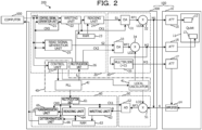
- FIG. 2 is a diagram illustrating a specific exemplary configuration of the information processing system including the information processing apparatus according to the embodiment illustrated in FIG. 1 .
- the information processing apparatus 100 includes the cooler 10 and a control device 300.
- the control device 300 is a device that controls the cooler 10 in accordance with the command cmd input from the computer 500.
- the control device 300 includes the digital circuit 20, the conversion circuit 30, the adjustment circuit 40, the conversion circuit 50, and the digital circuit 60.
- the control device 300 generates a plurality of microwaves M1, M2, and M3 having different frequencies in accordance with the command cmd input from the computer 500, and transmits them to the cooler 10.
- the microwave M1 is a control signal to be used to control the state of the quantum bit 11.
- the microwave M2 is a read signal to be used to read the state of the quantum bit 11.
- the microwave M3 is a pump signal to be used for an amplifier 14 that parametrically amplifies a signal representing the read result of the state of the quantum bit 11.
- the cooler 10 cools the quantum bit 11.
- the cooler 10 includes, for example, the quantum bit 11, attenuators (ATTs) 15, 16, and 17, and the amplifier 14.
- the quantum bit 11 includes a resonator 12 to be used to control the state of the quantum bit 11, and a resonator 13 to be used to read the state of the quantum bit 11.
- the attenuators 15, 16, and 17 attenuate the corresponding microwaves M1, M2, and M3, respectively.
- the amplifier 14 is a parametric amplifier that parametrically amplifies the signals representing the state of the quantum bit 11 read by the resonator 13.
- the digital circuit 20 generates the digital signals S in accordance with the command cmd input from the computer 500.
- the digital circuit 20 includes, for example, a control signal generation unit 21, a writing unit 22, a random access memory (RAM) 23, a reading unit 24, a read signal generation unit 25, a multiplication unit 26, and a control unit 27.
- the digital circuit 20 is implemented by, for example, a field programmable gate array (FPGA), an application specific integrated circuit (ASIC), a microcomputer, or the like.
- the control signal generation unit 21 generates a control signal for controlling the state of the quantum bit 11 in accordance with the command cmd input from the computer 500.
- the writing unit 22 temporarily stores the control signal generated by the control signal generation unit 21 in the RAM 23.
- the reading unit 24 reads the control signal from the RAM 23, and outputs the read control signal as a digital signal S1.
- the read signal generation unit 25 generates a read signal for reading the state of the quantum bit 11 in accordance with the command cmd input from the computer 500.
- the read signal generation unit 25 outputs the generated read signal as a digital signal S2.
- the control unit 27 controls frequency adjustment of a phase locked loop (PLL 42) in accordance with the command cmd input from the computer 500.
- the PLL 42 outputs the use frequency f 0 in accordance with the command cmd, and adjusts the use frequency f 0 to the frequency specified by the command cmd.
- the multiplication unit 26 generates clock signals CK0, CK1, and CK2 having frequencies obtained by multiplying the use frequency f 0 .
- the frequencies of the clock signals CK0, CK1, and CK2 are different from each other.
- the control signal generation unit 21 and the writing unit 22 operate according to the clock signal CK0 used in an interface with the computer 500.
- the reading unit 24 and a DA converter 31 operate according to the clock signal CK1 for DA conversion.
- a DA converter 33 operates according to the clock signal CK2 for DA conversion.
- the conversion circuit 30 includes the DA converter 31, a mixer 32, the DA converter 33, a mixer 34, and a multiplier 35.
- the DA converter 31 is a circuit that converts the digital signal S1 into an analog signal RF1.
- the analog signal RF1 is a radio frequency (RF) signal.
- a frequency of the analog signal RF1 changes as the use frequency f 0 changes.
- the mixer 32 up-converts the analog signal RF1 into the microwave M1 by multiplying the analog signal RF1 by a local oscillation signal LO1.
- the local oscillation signal LO1 has a frequency higher than that of the analog signal RF1.
- the DA converter 33 is a circuit that converts the digital signal S2 into an analog signal RF2.
- the analog signal RF2 is an RF signal.
- a frequency of the analog signal RF2 changes as the use frequency f 0 changes.
- the mixer 34 up-converts the analog signal RF2 into the microwave M2 by multiplying the analog signal RF2 by a local oscillation signal LO2.
- the local oscillation signal LO2 has a frequency higher than that of the analog signal RF2.
- the multiplier 35 generates the microwave M3 having a frequency twice the frequency of the microwave M2.
- the adjustment circuit 40 adjusts the use frequency f 0 such that the multiplication of the frequency of the analog signal RF1 differs from a predetermined frequency F1 (in this example, the resonance frequency of the resonator 12 used to control the state of the quantum bit 11). As a result, noise of a harmonic component that affects resonance of the resonator 12 may be reduced. Furthermore, the adjustment circuit 40 adjusts the use frequency f 0 such that the multiplication of the frequency of the analog signal RF2 differs from a predetermined frequency F2 (in this example, the resonance frequency of the resonator 13 used to read the state of the quantum bit 11). As a result, noise of a harmonic component that affects resonance of the resonator 13 may be reduced.
- the adjustment circuit 40 may include a local oscillator 41 that adjusts the frequency of the local oscillation signal LO1 input to the mixer 32 so that the frequency of the microwave M1 matches the predetermined frequency F1 (in this example, the resonance frequency of the resonator 12 used to control the state of the quantum bit 11).
- F1 the predetermined frequency
- F1 the resonance frequency of the resonator 12 used to control the state of the quantum bit 11
- the adjustment circuit 40 may include the local oscillator 41 that adjusts the frequency of the local oscillation signal LO2 input to the mixer 34 so that the frequency of the microwave M2 matches the predetermined frequency F2 (in this example, the resonance frequency of the resonator 13 used to read the state of the quantum bit 11).
- F2 the predetermined frequency
- F2 the resonance frequency of the resonator 13 used to read the state of the quantum bit 11
- the adjustment circuit 40 may include the local oscillator 41 that adjusts the frequency of the local oscillation signal LO2 input to the mixer 34 so that the frequency of the microwave M3 matches a predetermined frequency F3 (in this example, the frequency twice the resonance frequency of the resonator 13).
- F3 in this example, the frequency twice the resonance frequency of the resonator 13
- the adjustment circuit 40 includes the control unit 27, the local oscillator 41, and the PLL 42.
- the local oscillator 41 is an example of a first adjustment circuit that adjusts the frequencies of the microwaves, and in this example, it adjusts the frequencies of the microwaves M1, M2, and M3 according to a first frequency adjustment signal output from the control unit 27.
- the PLL 42 is an example of a second adjustment circuit that adjusts the use frequency f 0 , and in this example, it adjusts the use frequency f 0 according to a second frequency adjustment signal output from the control unit 27.
- the adjustment circuit 40 performs adjustment such that the multiplication of the use frequency f 0 differs from the frequencies of the microwaves M1, M2, and M3 using at least one of the local oscillator 41 or the PLL 42. As a result, the noise of the harmonic component that affects the control and reading of the quantum bit 11 may be reduced.
- the local oscillator 41 adjusts the frequencies of the microwaves M1, M2, and M3 to the respective predetermined frequencies F1, F2, and F3 corresponding thereto according to the first frequency adjustment signal output from the control unit 27.
- the PLL 42 adjusts the use frequency f 0 such that the multiplication of the use frequency f 0 differs from the predetermined frequencies F1, F2, and F3 according to the second frequency adjustment signal output from the control unit 27.
- the multiplication unit 26 multiplies the use frequency f 0 of 500 MHz by a factor of four and the DA converter 31 generates the analog signal RF1 of 2 GHz.
- the local oscillator 41 compensates for this difference in the frequency with the local oscillation signal LO1 in the microwave frequency band. Specifically, it is assumed that the frequency of the microwave M1 is adjusted to 10 GHz by the analog signal RF1 of 2 GHz and the local oscillation signal LO1 of 8 GHz.
- the PLL 42 changes the use frequency f 0 to 490 MHz, and the local oscillator 41 changes the frequency of the local oscillation signal LO1 to 8.04 GHz.
- the frequency of the microwave M1 is maintained at 10 GHz by the analog signal RF1 of 1.96 GHz and the local oscillation signal LO1 of 8.04 GHz.
- the other microwaves M2 and M3 are treated in a similar manner.
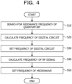
- FIG. 4 is a flowchart illustrating a first example of a frequency adjustment method.
- the frequency adjustment method illustrated in FIG. 4 is implemented by the control device 300 operating in accordance with the command cmd from the computer 500.
- a frequency adjustment program for causing the computer 500 to execute each processing illustrated in FIG. 4 is stored in the auxiliary storage device 502 described above.
Landscapes
- Engineering & Computer Science (AREA)
- Theoretical Computer Science (AREA)
- General Physics & Mathematics (AREA)
- Physics & Mathematics (AREA)
- General Engineering & Computer Science (AREA)
- Condensed Matter Physics & Semiconductors (AREA)
- Evolutionary Computation (AREA)
- Data Mining & Analysis (AREA)
- Mathematical Analysis (AREA)
- Mathematical Optimization (AREA)
- Pure & Applied Mathematics (AREA)
- Computing Systems (AREA)
- Computational Mathematics (AREA)
- Mathematical Physics (AREA)
- Software Systems (AREA)
- Artificial Intelligence (AREA)
- Stabilization Of Oscillater, Synchronisation, Frequency Synthesizers (AREA)
Abstract
Description
- The present disclosure relates to an information processing apparatus, a frequency adjustment method, and a frequency adjustment program.
- A quantum bit device to be used in a quantum computer using a superconducting circuit including a Josephson junction has been commonly known.
- The quantum bit device includes a quantum bit placed in a dilution refrigerator, a control line that controls a state of the quantum bit, and a quantum bit control unit that generates microwaves to be transmitted to the control line (e.g., see Patent Document 1).
- However, when digital signals are generated in the quantum computer, harmonic noise generated by the digital signals may be superimposed on the microwaves.
- The present disclosure provides an information processing apparatus, a frequency adjustment method, and a frequency adjustment program capable of reducing harmonic noise superimposed on microwaves.
- In one aspect of the present disclosure, there is provided an information processing apparatus including: a quantum bit; a digital circuit configured to generate a digital signal; a conversion circuit configured to convert the digital signal into a microwave to be transmitted to the quantum bit; and an adjustment circuit configured to set a first frequency of a clock used in the digital circuit such that a harmonic frequency of the first frequency differs from a second frequency of the microwave.
- According to the present disclosure, harmonic noise superimposed on microwaves may be reduced.
-
-
FIG. 1 is a diagram illustrating an exemplary configuration of an information processing system including an information processing apparatus according to an embodiment. -
FIG. 2 is a diagram illustrating a specific exemplary configuration of the information processing system including the information processing apparatus according to the embodiment. -
FIG. 3 is a hardware configuration diagram of a computer. -
FIG. 4 is a flowchart illustrating a first example of a frequency adjustment method. -
FIG. 5 is a flowchart illustrating a second example of the frequency adjustment method. - Hereinafter, an embodiment will be described.
-
FIG. 1 is a diagram illustrating an exemplary configuration of an information processing system including an information processing apparatus according to an embodiment. Aninformation processing system 200 illustrated inFIG. 1 is a system that processes information using acomputer 500. Theinformation processing system 200 includes aninformation processing apparatus 100 and thecomputer 500. Theinformation processing apparatus 100 is coupled to thecomputer 500 by wire or wirelessly. - The
information processing apparatus 100 processes information using aquantum bit 11 in accordance with a command cmd input from thecomputer 500. Theinformation processing apparatus 100 is also called a quantum computer. Theinformation processing apparatus 100 exemplified inFIG. 1 includes acooler 10, adigital circuit 20, aconversion circuit 30, anadjustment circuit 40, aconversion circuit 50, and adigital circuit 60. - The
cooler 10 cools thequantum bit 11. Thecooler 10 is, for example, a dilution refrigerator that uses heat of dilution generated when liquid helium-3 is diluted into liquid helium-4. Thecooler 10 may be a device that cools thequantum bit 11 by another cooling method. - The
quantum bit 11 puts information on a quantum-mechanical two-state system. The quantum bit is also called a qubit. Thequantum bit 11 is, for example, a superconducting quantum bit formed by a superconducting circuit including a superconducting Josephson junction. The type of thequantum bit 11 is not limited to this. The number of thequantum bits 11 is at least one or more. - The
digital circuit 20 generates digital signals S. Thedigital circuit 20 generates the digital signals S corresponding to the content of the command cmd in accordance with the command cmd supplied from thecomputer 500, for example. - The
conversion circuit 30 converts the digital signals S generated by thedigital circuit 20 into microwaves M to be transmitted to thecooler 10. A frequency of the microwaves M is higher than a frequency (use frequency f0) used in thedigital circuit 20. The use frequency f0 is an example of a first frequency of a clock used in the digital circuit. The frequency of the microwaves M is an example of a second frequency of the microwaves transmitted to the quantum bit or the cooler. - The
adjustment circuit 40 has a function of adjusting the frequency of the microwaves M to a predetermined frequency F (e.g., resonance frequency of the quantum bit 11), and a function of multiplying the clock of the frequency f0 used in thedigital circuit 20. Here, theadjustment circuit 40 has a function of performing adjustment such that an integral multiple of the frequency f0 (frequency of harmonics) differs from the predetermined frequency F. Therefore, harmonics having a frequency obtained by multiplying the use frequency f0 do not appear at the frequency (predetermined frequency F) of the microwave M, whereby a malfunction of the cooler 10 (in particular, quantum bit 11) due to noise of the harmonics may be reduced. - For example, the
adjustment circuit 40 adjusts the use frequency f0 such that the multiplication of the use frequency f0 differs from the predetermined frequency F. When thedigital circuit 20 is operated at 500 MHz (when the use frequency f0 is 500 MHz) in the case where the predetermined frequency F is set to 10.00 GHz, for example, harmonics multiplied by a factor of 20 appear at 10.00 GHz as harmonic noise. Theadjustment circuit 40 adjusts the operation frequency of thedigital circuit 20 to 490 MHz (adjusts the use frequency f0 to 490 MHz), whereby the frequency of the harmonics shifts to 9.80 GHz (= 490 MHz × 20). Thus, the harmonic noise obtained by multiplying the use frequency f0 by a factor of 20 does not appear at 10.00 GHz. - The quantum computer performs control using weak power of equal to or lower than -100 dBm. However, in the digital circuit that generates digital signals, there is large noise such as digital noise. Thus, a scheme is considered in which an S component is increased to increase a signal-to-noise ratio (SNR), and then the entire signals are attenuated using an attenuator (ATT). However, according to this scheme, the power of the S component increases, whereby power consumption may increase. In addition, resolving power of lower bits of a digital-to-analog (DA) converter for converting digital signals into analog signals is wasted, and accordingly, a dynamic range may be narrowed.
- Furthermore, one of factors of the noise generated by the digital circuit is clock signals. In the quantum computer, there may be a plurality of "bands in which the harmonics are not desired to be applied (e.g., resonance frequency of the quantum bit, etc.)", and they may deviate from a design value. Thus, it is difficult to calculate the frequency of the clock signals in advance at the time of designing such that the frequency of the harmonics of the clock signals is out of the "bands in which the harmonics are not desired to be applied". Furthermore, when a filter for removing the harmonics of the clock signals and the digital signals is used or the accuracy of the clock signals is lowered, the quality of the microwaves transmitted to the cooler may be lowered.
- In view of those problems, the
adjustment circuit 40 performs adjustment such that the multiplication of the use frequency f0 differs from the microwaves M in the present embodiment. As a result, the factors of generating the harmonic noise superimposed on the microwaves M are reduced or removed, whereby the harmonic noise superimposed on the microwaves M may be reduced. - The
conversion circuit 50 converts an analog output signal A output from thecooler 10 into a digital output signal B. The output signal B is a digital signal representing a read result of a state of thequantum bit 11. - The
digital circuit 60 performs predetermined processing on the digital output signal B from theconversion circuit 50, and outputs it to thecomputer 500 as read data d. - In a case where the microwaves M are signals to be used to control the state of the
quantum bit 11 or signals to be used to read the state of thequantum bit 11, the state of thequantum bit 11 may be read from thequantum bit 11 when the frequency of the microwaves M matches the resonance frequency of thequantum bit 11. Theadjustment circuit 40 adjusts the frequency of the microwaves M to the resonance frequency of thequantum bit 11 so that the state of thequantum bit 11 is read from the output signal A transmitted from thequantum bit 11 or the cooler 10 (e.g., as read from the output signal B or digital data d). As a result, the read data d representing the read result of the state of thequantum bit 11 may be supplied to thecomputer 500, and thecomputer 500 is enabled to obtain the read data d from thedigital circuit 60. - The resonance frequency of the
quantum bit 11 may drift every manufacturing variation of thequantum bit 11 or every activation of thequantum bit 11. Theadjustment circuit 40 may observe the output signal A for each activation of thequantum bit 11, and may adjust the frequency of the microwaves M to the resonance frequency of thequantum bit 11 for each activation of thequantum bit 11 so that the state of thequantum bit 11 is read from the output signal A. As a result, even if the resonance frequency of thequantum bit 11 deviates from the design value, the read data d representing the read result of the state of thequantum bit 11 may be supplied to thecomputer 500, and thecomputer 500 is enabled to obtain the read data d from thedigital circuit 60. - The
adjustment circuit 40 may adjust the use frequency f0 such that the SNR of the microwaves M looped back before being input to the cooler 10 satisfies a predetermined reference value. As a result, the harmonics (e.g., harmonics generated in the microwaves M by operation of software, etc.) obtained by multiplying a frequency not intended by a designer may be reduced. - Next, a specific exemplary configuration of the information processing system will be described.
-
FIG. 2 is a diagram illustrating a specific exemplary configuration of the information processing system including the information processing apparatus according to the embodiment illustrated inFIG. 1 . Theinformation processing apparatus 100 includes the cooler 10 and acontrol device 300. Thecontrol device 300 is a device that controls the cooler 10 in accordance with the command cmd input from thecomputer 500. Thecontrol device 300 includes thedigital circuit 20, theconversion circuit 30, theadjustment circuit 40, theconversion circuit 50, and thedigital circuit 60. - The
control device 300 generates a plurality of microwaves M1, M2, and M3 having different frequencies in accordance with the command cmd input from thecomputer 500, and transmits them to the cooler 10. The microwave M1 is a control signal to be used to control the state of thequantum bit 11. The microwave M2 is a read signal to be used to read the state of thequantum bit 11. The microwave M3 is a pump signal to be used for anamplifier 14 that parametrically amplifies a signal representing the read result of the state of thequantum bit 11. - The cooler 10 cools the
quantum bit 11. The cooler 10 includes, for example, thequantum bit 11, attenuators (ATTs) 15, 16, and 17, and theamplifier 14. Thequantum bit 11 includes aresonator 12 to be used to control the state of thequantum bit 11, and aresonator 13 to be used to read the state of thequantum bit 11. Theattenuators amplifier 14 is a parametric amplifier that parametrically amplifies the signals representing the state of thequantum bit 11 read by theresonator 13. - The
digital circuit 20 generates the digital signals S in accordance with the command cmd input from thecomputer 500. Thedigital circuit 20 includes, for example, a controlsignal generation unit 21, awriting unit 22, a random access memory (RAM) 23, areading unit 24, a readsignal generation unit 25, amultiplication unit 26, and acontrol unit 27. Thedigital circuit 20 is implemented by, for example, a field programmable gate array (FPGA), an application specific integrated circuit (ASIC), a microcomputer, or the like. - The control
signal generation unit 21 generates a control signal for controlling the state of thequantum bit 11 in accordance with the command cmd input from thecomputer 500. Thewriting unit 22 temporarily stores the control signal generated by the controlsignal generation unit 21 in the RAM 23. Thereading unit 24 reads the control signal from the RAM 23, and outputs the read control signal as a digital signal S1. - The read
signal generation unit 25 generates a read signal for reading the state of thequantum bit 11 in accordance with the command cmd input from thecomputer 500. The readsignal generation unit 25 outputs the generated read signal as a digital signal S2. - The
control unit 27 controls frequency adjustment of a phase locked loop (PLL 42) in accordance with the command cmd input from thecomputer 500. ThePLL 42 outputs the use frequency f0 in accordance with the command cmd, and adjusts the use frequency f0 to the frequency specified by the command cmd. Themultiplication unit 26 generates clock signals CK0, CK1, and CK2 having frequencies obtained by multiplying the use frequency f0. The frequencies of the clock signals CK0, CK1, and CK2 are different from each other. - The control
signal generation unit 21 and thewriting unit 22 operate according to the clock signal CK0 used in an interface with thecomputer 500. Thereading unit 24 and aDA converter 31 operate according to the clock signal CK1 for DA conversion. ADA converter 33 operates according to the clock signal CK2 for DA conversion. - The
conversion circuit 30 includes theDA converter 31, amixer 32, theDA converter 33, amixer 34, and amultiplier 35. - The
DA converter 31 is a circuit that converts the digital signal S1 into an analog signal RF1. The analog signal RF1 is a radio frequency (RF) signal. A frequency of the analog signal RF1 changes as the use frequency f0 changes. Themixer 32 up-converts the analog signal RF1 into the microwave M1 by multiplying the analog signal RF1 by a local oscillation signal LO1. The local oscillation signal LO1 has a frequency higher than that of the analog signal RF1. - The
DA converter 33 is a circuit that converts the digital signal S2 into an analog signal RF2. The analog signal RF2 is an RF signal. A frequency of the analog signal RF2 changes as the use frequency f0 changes. Themixer 34 up-converts the analog signal RF2 into the microwave M2 by multiplying the analog signal RF2 by a local oscillation signal LO2. The local oscillation signal LO2 has a frequency higher than that of the analog signal RF2. Themultiplier 35 generates the microwave M3 having a frequency twice the frequency of the microwave M2. - The
adjustment circuit 40 adjusts the use frequency f0 such that the multiplication of the frequency of the analog signal RF1 differs from a predetermined frequency F1 (in this example, the resonance frequency of theresonator 12 used to control the state of the quantum bit 11). As a result, noise of a harmonic component that affects resonance of theresonator 12 may be reduced. Furthermore, theadjustment circuit 40 adjusts the use frequency f0 such that the multiplication of the frequency of the analog signal RF2 differs from a predetermined frequency F2 (in this example, the resonance frequency of theresonator 13 used to read the state of the quantum bit 11). As a result, noise of a harmonic component that affects resonance of theresonator 13 may be reduced. - The
adjustment circuit 40 may include alocal oscillator 41 that adjusts the frequency of the local oscillation signal LO1 input to themixer 32 so that the frequency of the microwave M1 matches the predetermined frequency F1 (in this example, the resonance frequency of theresonator 12 used to control the state of the quantum bit 11). As a result, it becomes possible to achieve both reduction of the noise of the harmonic component that affects the resonance of theresonator 12 and control of the frequency of the microwave M1 to the frequency at which theresonator 12 resonates. - The
adjustment circuit 40 may include thelocal oscillator 41 that adjusts the frequency of the local oscillation signal LO2 input to themixer 34 so that the frequency of the microwave M2 matches the predetermined frequency F2 (in this example, the resonance frequency of theresonator 13 used to read the state of the quantum bit 11). As a result, it becomes possible to achieve both reduction of the noise of the harmonic component that affects the resonance of theresonator 13 and control of the frequency of the microwave M2 to the frequency at which theresonator 13 resonates. - The
adjustment circuit 40 may include thelocal oscillator 41 that adjusts the frequency of the local oscillation signal LO2 input to themixer 34 so that the frequency of the microwave M3 matches a predetermined frequency F3 (in this example, the frequency twice the resonance frequency of the resonator 13). As a result, it becomes possible to achieve both reduction of the noise of the harmonic component that affects the parametric amplification of theamplifier 14 and control of the frequency of the microwave M3 to the frequency at which theamplifier 14 parametrically oscillates. - In this example, the
adjustment circuit 40 includes thecontrol unit 27, thelocal oscillator 41, and thePLL 42. Thelocal oscillator 41 is an example of a first adjustment circuit that adjusts the frequencies of the microwaves, and in this example, it adjusts the frequencies of the microwaves M1, M2, and M3 according to a first frequency adjustment signal output from thecontrol unit 27. ThePLL 42 is an example of a second adjustment circuit that adjusts the use frequency f0, and in this example, it adjusts the use frequency f0 according to a second frequency adjustment signal output from thecontrol unit 27. Theadjustment circuit 40 performs adjustment such that the multiplication of the use frequency f0 differs from the frequencies of the microwaves M1, M2, and M3 using at least one of thelocal oscillator 41 or thePLL 42. As a result, the noise of the harmonic component that affects the control and reading of thequantum bit 11 may be reduced. - In this example, the
local oscillator 41 adjusts the frequencies of the microwaves M1, M2, and M3 to the respective predetermined frequencies F1, F2, and F3 corresponding thereto according to the first frequency adjustment signal output from thecontrol unit 27. Meanwhile, thePLL 42 adjusts the use frequency f0 such that the multiplication of the use frequency f0 differs from the predetermined frequencies F1, F2, and F3 according to the second frequency adjustment signal output from thecontrol unit 27. As a result, it becomes possible to achieve both reduction of the noise of the harmonic component that affects the control and reading of the state of thequantum bit 11 and control of the frequencies of the individual microwaves to the individual predetermined frequencies. - For example, a case will be considered where the
multiplication unit 26 multiplies the use frequency f0 of 500 MHz by a factor of four and theDA converter 31 generates the analog signal RF1 of 2 GHz. When thePLL 42 changes the use frequency f0 to 490 MHz, the frequency of the analog signal RF1 decreases to 1.96 GHz (= 490 MHz × 4). Thelocal oscillator 41 compensates for this difference in the frequency with the local oscillation signal LO1 in the microwave frequency band. Specifically, it is assumed that the frequency of the microwave M1 is adjusted to 10 GHz by the analog signal RF1 of 2 GHz and the local oscillation signal LO1 of 8 GHz. ThePLL 42 changes the use frequency f0 to 490 MHz, and thelocal oscillator 41 changes the frequency of the local oscillation signal LO1 to 8.04 GHz. As a result, the frequency of the microwave M1 is maintained at 10 GHz by the analog signal RF1 of 1.96 GHz and the local oscillation signal LO1 of 8.04 GHz. The other microwaves M2 and M3 are treated in a similar manner. - The
conversion circuit 50 converts an analog output signal A output from the cooler 10 into a digital output signal B. Theconversion circuit 50 includes amixer 51 and an analog-to-digital (AD)converter 52. - The
mixer 51 down-converts the analog output signal A into an analog signal RF3 by multiplying the analog output signal A output from theamplifier 14 by a local oscillation signal LO3. The local oscillation signal LO3 has a frequency lower than that of the analog output signal A. The analog signal RF3 is an RF signal. TheAD converter 52 is a circuit that converts the analog signal RF3 into a digital signal B. - The
digital circuit 60 generates read data d from the digital signal B in accordance with the command cmd input from thecomputer 500. Thedigital circuit 60 includes, for example, a writing unit 62, aRAM 63, areading unit 64, atransmission unit 65, amultiplication unit 61, and adetermination unit 66. Thedigital circuit 60 is implemented by, for example, an FPGA, an ASIC, a microcomputer, or the like. - The writing unit 62 temporarily stores the digital signal B in the
RAM 63. Thereading unit 64 reads the digital signal B from theRAM 63, and converts the read digital signal B into the read data d. Thetransmission unit 65 transmits the read data d to thecomputer 500. Thedetermination unit 66 determines whether or not the SNR of the microwave M1 (which may be the microwave M2 or the microwave M3) looped back before being input to the cooler 10 satisfies a predetermined reference value, and outputs the read data d including a result of the determination to thecomputer 500. Themultiplication unit 61 generates the clock signals CK0 and CK1 having frequencies obtained by multiplying the use frequency f0. The frequencies of the clock signals CK0 and CK1 are different from each other. - The writing unit 62 and the
AD converter 52 operate according to the clock signal CK1 for AD conversion. Thedetermination unit 66, thetransmission unit 65, and thereading unit 64 operate according to the clock signal CK0 used in the interface with thecomputer 500. -
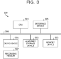
FIG. 3 is a hardware configuration diagram of the computer. Thecomputer 500 illustrated inFIG. 3 includes adrive device 501, anauxiliary storage device 502, amemory device 503, a central processing unit (CPU) 504, andinterface device 505, and the like, which are mutually coupled to each other by abus 506. - A program that implements processing in the
computer 500 is provided by arecording medium 507. When therecording medium 507 recording the program is set in thedrive device 501, the program is installed in theauxiliary storage device 502 from therecording medium 507 via thedrive device 501. However, the program is not necessarily installed from therecording medium 507, and may be downloaded from another computer via a network. Theauxiliary storage device 502 stores the installed program, and also stores files, data, and the like that are needed. - The
memory device 503 reads the program from theauxiliary storage device 502 and stores it when an instruction to start the program is issued. TheCPU 504 is a processor that implements functions related to thecomputer 500 in accordance with the program stored in thememory device 503. Theinterface device 505 is used as an interface for coupling to the outside. - Note that examples of the
recording medium 507 include a portable recording medium such as a compact disc read only memory (CD-ROM), a digital versatile disc (DVD), a universal serial bus (USB) memory, or the like. Furthermore, examples of theauxiliary storage device 502 include a hard disk drive (HDD), a flash memory, and the like. Both therecording medium 507 and theauxiliary storage device 502 correspond to a computer-readable recording medium. -
FIG. 4 is a flowchart illustrating a first example of a frequency adjustment method. The frequency adjustment method illustrated inFIG. 4 is implemented by thecontrol device 300 operating in accordance with the command cmd from thecomputer 500. A frequency adjustment program for causing thecomputer 500 to execute each processing illustrated inFIG. 4 is stored in theauxiliary storage device 502 described above. - In step S10, the
computer 500 outputs a command cmd (search command) for searching for the resonance frequency of thequantum bit 11. Theadjustment circuit 40 sweeps the use frequency f0 from the design value in accordance with the search command. As a result, the frequency of the microwave M1 transmitted from theconversion circuit 30 sweeps from the design value. Thecomputer 500 refers to the read data d generated by theconversion circuit 50 and thedigital circuit 60 based on the output signal A transmitted from the cooler 10, and searches for a frequency reactive to the read data d. A search result of the frequency having a reaction is stored in a storage device of thecomputer 500 as a predetermined frequency F1. Likewise, thecomputer 500 sweeps the frequencies of the microwaves M2 and M3, searches for frequencies reactive to the read data d, and stores, in the storage device, a search result of the frequencies having a reaction as predetermined frequencies F2 and F3. - In step S20, the
computer 500 calculates the use frequency f0 in thedigital circuit 20. Thecomputer 500 determines whether or not the multiplication of the use frequency f0 matches the predetermined frequencies F1, F2, and F3. If the multiplication of the use frequency f0 does not match the predetermined frequencies F1, F2, and F3, thecomputer 500 outputs a command cmd (first setting command) for setting the use frequency f0. On the other hand, if the multiplication of the use frequency f0 matches the predetermined frequencies F1, F2, and F3, thecomputer 500 outputs a command cmd (first setting command) for changing the use frequency f0 in units of, for example, 0.1 MHz. - In step S30, the
control unit 27 of theadjustment circuit 40 sets the use frequency f0 generated by thePLL 42 to the frequency specified by the first setting command. - In step S40, the
computer 500 calculates frequencies of the analog signals RF1 and RF2 that change according to the use frequency f0 set in step S30. - In step S50, the
computer 500 sets the frequencies of the microwaves M1, M2, and M3. Thecomputer 500 outputs a command cmd (second setting command) for setting the frequency of the local oscillation signal LO1 such that the frequency of the microwave M1 matches the predetermined frequency F1 by the analog signal RF1 calculated in step S40. Thecontrol unit 27 of theadjustment circuit 40 sets the frequency of the local oscillation signal LO1 to the frequency specified by the second setting command. Likewise, thecomputer 500 outputs a command cmd (second setting command) for setting the frequency of the local oscillation signal LO2 such that the frequency of the microwave M2 matches the predetermined frequency F2 by the analog signal RF2 calculated in step S40. Thecontrol unit 27 of theadjustment circuit 40 sets the frequency of the local oscillation signal LO2 to the frequency specified by the second setting command. - As described above, since the
information processing apparatus 100 according to the present embodiment has the two frequency variable functions of thePLL 42 and thelocal oscillator 41, a degree of freedom regarding the setting range of the frequencies of the microwaves increases as compared with a form including only one frequency variable function. As a result, it is easy to achieve both reduction of the noise of the harmonic component that affects the control and reading of the state of thequantum bit 11 and control of the frequencies of the individual microwaves to the individual predetermined frequencies. -
FIG. 5 is a flowchart illustrating a second example of the frequency adjustment method. The frequency adjustment method illustrated inFIG. 5 is implemented by thecontrol device 300 operating in accordance with the command cmd from thecomputer 500. The frequency adjustment program for causing thecomputer 500 to execute each processing illustrated inFIG. 5 is stored in theauxiliary storage device 502 described above. Since descriptions of steps S10, S20, S30, S40, and S50 are similar to those ofFIG. 4 , they will be omitted. - In step S60, the
computer 500 obtains, from the read data d, a measurement result of the SNR of the resonance frequency of thequantum bit 11 by thedetermination unit 66. As a result, thecomputer 500 is enabled to grasp the harmonics (e.g., harmonics generated in the microwave M1 or the like by operation of software, etc.) obtained by multiplying a frequency not intended by the designer. - In step S70, the
computer 500 determines whether or not the SNR satisfies a predetermined reference value. If the SNR does not satisfy the predetermined reference value, thecomputer 500 returns to the processing of step S20. In step S20, thecomputer 500 recalculates the use frequency f0 in thedigital circuit 20 such that the multiplication of the use frequency f0 is not a frequency that matches the predetermined frequencies F1, F2, and F3. As a result, the harmonics (e.g., harmonics generated in the microwave M1 or the like by operation of software, etc.) obtained by multiplying a frequency not intended by the designer may be reduced. - For example, in a case where a width of the resonance frequency of the
quantum bit 11 is set to a and harmonic noise exists within a range of ±a/2 from the center of a, thecomputer 500 changes the use frequency f0 such that the resonance frequency of thequantum bit 11 changes in units of a/2. - Although the embodiment has been described above, the technique of the present disclosure is not limited to the embodiment described above. Various modifications and improvements, such as combination and replacement with some or all of other embodiments, may be made.
- Patent Document 1:
Japanese Laid-open Patent Publication No. 2007-49009 -
- 10 Cooler
- 11 Quantum bit
- 12, 13 Resonator
- 14 Amplifier
- 15, 16, 17 Attenuator
- 20 Digital circuit
- 30 Conversion circuit
- 40 Adjustment circuit
- 50 Conversion circuit
- 60 Digital circuit
- 100 Information processing apparatus
- 200 Information processing system
- 300 Control device
- 500 Computer
- A Output signal
- B Digital signal
- M Microwave
- S Digital signal
Claims (17)
- An information processing apparatus comprising:a quantum bit;a digital circuit configured to generate a digital signal;a conversion circuit configured to convert the digital signal into a microwave to be transmitted to the quantum bit; andan adjustment circuit configured to set a first frequency of a clock used in the digital circuit such that a harmonic frequency of the first frequency differs from a second frequency of the microwave.
- The information processing apparatus according to claim 1, wherein the adjustment circuit is configured to set the second frequency to a predetermined frequency, and set the first frequency such that an integral multiple of the first frequency differs from the predetermined frequency.
- The information processing apparatus according to claim 2, whereinthe conversion circuit includes: a converter configured to convert the digital signal into an analog signal, and a mixer configured to up-convert the analog signal into the microwave,the second frequency changes with a change of the first frequency, andthe adjustment circuit adjusts the first frequency such that the integral multiple of the first frequency differs from the predetermined frequency.
- The information processing apparatus according to claim 3, wherein the adjustment circuit is configured to adjust a frequency of a local oscillation signal to be input to the mixer such that the second frequency matches the predetermined frequency.
- The information processing apparatus according to claim 1, whereinthe adjustment circuit includes:a first adjustment circuit configured to adjust the second frequency; anda second adjustment circuit configured to adjust the first frequency, andthe adjustment circuit performs adjustment such that an integral multiple of the first frequency differs from the second frequency by using at least one of the first adjustment circuit or the second adjustment circuit.
- The information processing apparatus according to claim 5, whereinthe first adjustment circuit is configured to adjust the second frequency to a predetermined frequency, andthe second adjustment circuit is configured to adjust the first frequency such that the integral multiple of the first frequency differs from the predetermined frequency.
- The information processing apparatus according to any one of claims 1 to 6, wherein the adjustment circuit is configured to adjust the first frequency such that a signal-to-noise ratio (SNR) of the microwave that has been looped back satisfies a reference value.
- The information processing apparatus according to any one of claims 2 to 4 and 6, wherein the predetermined frequency includes a resonance frequency of the quantum bit.
- The information processing apparatus according to claim 8, wherein the adjustment circuit is configured to adjust the second frequency to the resonance frequency such that a state of the quantum bit is read from an output signal from the quantum bit or from an output signal from a cooler that cools the quantum bit.
- The information processing apparatus according to claim 9, wherein the adjustment circuit is configured to observe the output signal for each activation, and adjust the second frequency to the resonance frequency for each activation such that the state of the quantum bit is read from the output signal.
- The information processing apparatus according to any one of claims 8 to 10, wherein the resonance frequency includes a resonance frequency of a resonator to be used to control a state of the quantum bit.
- The information processing apparatus according to any one of claims 8 to 10, wherein the resonance frequency includes a resonance frequency of a resonator to be used to read a state of the quantum bit.
- The information processing apparatus according to any one of claims 1 to 11, wherein the microwave includes a signal to be used to control a state of the quantum bit.
- The information processing apparatus according to any one of claims 1 to 10 and 12, wherein the microwave includes a signal to be used to read a state of the quantum bit.
- The information processing apparatus according to any one of claims 1 to 7, wherein the microwave includes a pump signal to be used for an amplifier that parametrically amplifies a signal that represents a read result of a state of the quantum bit.
- A frequency adjustment method comprising:generating a digital signal with a digital circuit;converting the digital signal into a microwave to be transmitted to a quantum bit with a conversion circuit; andadjusting, with an adjustment circuit, a first frequency such that an integral multiple of the first frequency of a clock used in the digital circuit differs from a second frequency of the microwave.
- A frequency adjustment program for causing a computer to perform processing comprising:generating a digital signal with a digital circuit;converting the digital signal into a microwave to be transmitted to a quantum bit with a conversion circuit; andadjusting, with an adjustment circuit, a first frequency such that an integral multiple of the first frequency of a clock used in the digital circuit differs from a second frequency of the microwave.
Applications Claiming Priority (1)
| Application Number | Priority Date | Filing Date | Title |
|---|---|---|---|
| PCT/JP2022/006386 WO2023157179A1 (en) | 2022-02-17 | 2022-02-17 | Information processing device, frequency adjustment method, and frequency adjustment program |
Publications (3)
| Publication Number | Publication Date |
|---|---|
| EP4482285A1 true EP4482285A1 (en) | 2024-12-25 |
| EP4482285A4 EP4482285A4 (en) | 2025-03-19 |
| EP4482285B1 EP4482285B1 (en) | 2026-02-25 |
Family
ID=87577825
Family Applications (1)
| Application Number | Title | Priority Date | Filing Date |
|---|---|---|---|
| EP22927081.4A Active EP4482285B1 (en) | 2022-02-17 | 2022-02-17 | Information processing device, frequency adjustment method, and frequency adjustment program |
Country Status (4)
| Country | Link |
|---|---|
| US (1) | US20250013902A1 (en) |
| EP (1) | EP4482285B1 (en) |
| JP (1) | JP7694793B2 (en) |
| WO (1) | WO2023157179A1 (en) |
Families Citing this family (1)
| Publication number | Priority date | Publication date | Assignee | Title |
|---|---|---|---|---|
| WO2026013819A1 (en) * | 2024-07-10 | 2026-01-15 | Ntt株式会社 | Information processing device, parameter conversion method, and program |
Family Cites Families (10)
| Publication number | Priority date | Publication date | Assignee | Title |
|---|---|---|---|---|
| JP4777718B2 (en) | 2005-08-11 | 2011-09-21 | 日本電信電話株式会社 | Quantum bit device and qubit control method |
| US8874060B2 (en) * | 2009-12-18 | 2014-10-28 | Silicon Laboratories Inc. | Radio frequency (RF) receiver with frequency planning and method therefor |
| US10295582B2 (en) * | 2016-06-30 | 2019-05-21 | International Business Machines Corporation | Read out of quantum states of microwave frequency qubits with optical frequency photons |
| US10885460B2 (en) * | 2018-08-28 | 2021-01-05 | International Business Machines Corporation | Dispersive-resistive hybrid attenuator for quantum microwave circuits |
| US10922166B2 (en) * | 2019-03-27 | 2021-02-16 | Intel Corporation | Apparatus and method for probabilistic error correction of a quantum computing system |
| US10971593B2 (en) | 2019-06-14 | 2021-04-06 | International Business Machines Corporation | Oxygen reservoir for low threshold voltage P-type MOSFET |
| US11509310B2 (en) * | 2019-06-17 | 2022-11-22 | Microsoft Technology Licensing, Llc | Charge locking circuits and control system for qubits |
| WO2020253292A1 (en) * | 2019-06-17 | 2020-12-24 | 合肥本源量子计算科技有限责任公司 | Quantum parameter amplifier |
| US12494783B2 (en) * | 2020-09-25 | 2025-12-09 | Intel Corporation | Quantum computing systems, apparatus, and methods |
| US12265883B2 (en) * | 2021-08-31 | 2025-04-01 | Uti Limited Partnership | Optomechanical interface for spin qubits |
-
2022
- 2022-02-17 EP EP22927081.4A patent/EP4482285B1/en active Active
- 2022-02-17 JP JP2024500815A patent/JP7694793B2/en active Active
- 2022-02-17 WO PCT/JP2022/006386 patent/WO2023157179A1/en not_active Ceased
-
2024
- 2024-08-01 US US18/791,820 patent/US20250013902A1/en active Pending
Also Published As
| Publication number | Publication date |
|---|---|
| WO2023157179A1 (en) | 2023-08-24 |
| JPWO2023157179A1 (en) | 2023-08-24 |
| EP4482285B1 (en) | 2026-02-25 |
| EP4482285A4 (en) | 2025-03-19 |
| JP7694793B2 (en) | 2025-06-18 |
| US20250013902A1 (en) | 2025-01-09 |
Similar Documents
| Publication | Publication Date | Title |
|---|---|---|
| US5764087A (en) | Direct digital to analog microwave frequency signal simulator | |
| US5898325A (en) | Dual tunable direct digital synthesizer with a frequency programmable clock and method of tuning | |
| US20090140896A1 (en) | Clock dithering process for reducing electromagnetic interference in d/a converters and apparatus for carrying out such process | |
| US8699985B1 (en) | Frequency generator including direct digital synthesizer and signal processor including the same | |
| US20250013902A1 (en) | Information processing apparatus, frequency adjustment method, and frequency adjustment program | |
| CN113162617B (en) | Low-phase-noise X-band frequency source and modulation method thereof | |
| Yu et al. | The performance and limitations of FPGA-based digital servos for atomic, molecular, and optical physics experiments | |
| CN114744999A (en) | Frequency hopping source implementation method and device, frequency hopping source, electronic equipment and storage medium | |
| US20220252694A1 (en) | Systems and Methods for Digital Signal Chirp Generation Using Frequency Multipliers | |
| CN117081588A (en) | A wideband low-phase noise agile frequency synthesizer and its signal synthesis method | |
| JPH0923158A (en) | Frequency synthesizer | |
| US7808328B2 (en) | Ring oscillator with constant gain | |
| CN119675662B (en) | Frequency source synthesis system and method based on frequency agile radar | |
| US12283964B2 (en) | Phase-locked loop frequency synthesizer and control method therefor | |
| US6859750B1 (en) | Ramp sweep synthesis control | |
| KR20230117827A (en) | External reference signal source generator for DDS chip operation | |
| AU2003296435A1 (en) | Wideband dds synthesizer | |
| JPH08256058A (en) | Signal generator | |
| JP2022113497A (en) | Determination method of clock frequency of frequency synthesizer | |
| US20020064237A1 (en) | Quadrature modulation apparatus, radio transmission apparatus using quadrature modulation apparatus and quadrature modulation method | |
| JP6428498B2 (en) | Signal generator | |
| CN222850902U (en) | Signal generating device, quantum computing measurement and control system and quantum computer | |
| JP7807413B2 (en) | High-frequency signal generator | |
| JP2026017025A (en) | Processing apparatus, processing method, and program | |
| CN121328758A (en) | A method, apparatus, and quantum computer for modulating arbitrary microwave signals |
Legal Events
| Date | Code | Title | Description |
|---|---|---|---|
| STAA | Information on the status of an ep patent application or granted ep patent |
Free format text: STATUS: THE INTERNATIONAL PUBLICATION HAS BEEN MADE |
|
| PUAI | Public reference made under article 153(3) epc to a published international application that has entered the european phase |
Free format text: ORIGINAL CODE: 0009012 |
|
| STAA | Information on the status of an ep patent application or granted ep patent |
Free format text: STATUS: REQUEST FOR EXAMINATION WAS MADE |
|
| 17P | Request for examination filed |
Effective date: 20240806 |
|
| AK | Designated contracting states |
Kind code of ref document: A1 Designated state(s): AL AT BE BG CH CY CZ DE DK EE ES FI FR GB GR HR HU IE IS IT LI LT LU LV MC MK MT NL NO PL PT RO RS SE SI SK SM TR |
|
| A4 | Supplementary search report drawn up and despatched |
Effective date: 20250217 |
|
| RIC1 | Information provided on ipc code assigned before grant |
Ipc: G06F 1/12 20060101ALI20250211BHEP Ipc: G06N 10/00 20220101ALI20250211BHEP Ipc: H10N 60/10 20230101AFI20250211BHEP |
|
| DAV | Request for validation of the european patent (deleted) | ||
| DAX | Request for extension of the european patent (deleted) | ||
| REG | Reference to a national code |
Ref country code: DE Ref country code: DE Ref legal event code: R079 Ref document number: 602022031394 Country of ref document: DE Free format text: PREVIOUS MAIN CLASS: H10N0060100000 Ipc: G06N0010000000 |
|
| GRAP | Despatch of communication of intention to grant a patent |
Free format text: ORIGINAL CODE: EPIDOSNIGR1 |
|
| STAA | Information on the status of an ep patent application or granted ep patent |
Free format text: STATUS: GRANT OF PATENT IS INTENDED |
|
| RIC1 | Information provided on ipc code assigned before grant |
Ipc: G06N 10/00 20220101AFI20251009BHEP Ipc: G06F 1/12 20060101ALI20251009BHEP Ipc: G06N 10/20 20220101ALI20251009BHEP |
|
| INTG | Intention to grant announced |
Effective date: 20251022 |
|
| GRAS | Grant fee paid |
Free format text: ORIGINAL CODE: EPIDOSNIGR3 |
|
| GRAA | (expected) grant |
Free format text: ORIGINAL CODE: 0009210 |
|
| STAA | Information on the status of an ep patent application or granted ep patent |
Free format text: STATUS: THE PATENT HAS BEEN GRANTED |
|
| AK | Designated contracting states |
Kind code of ref document: B1 Designated state(s): AL AT BE BG CH CY CZ DE DK EE ES FI FR GB GR HR HU IE IS IT LI LT LU LV MC MK MT NL NO PL PT RO RS SE SI SK SM TR |
|
| REG | Reference to a national code |
Ref country code: CH Ref legal event code: F10 Free format text: ST27 STATUS EVENT CODE: U-0-0-F10-F00 (AS PROVIDED BY THE NATIONAL OFFICE) Effective date: 20260225 Ref country code: GB Ref legal event code: FG4D |
|
| REG | Reference to a national code |
Ref country code: DE Ref legal event code: R096 Ref document number: 602022031394 Country of ref document: DE |
|
| REG | Reference to a national code |
Ref country code: IE Ref legal event code: FG4D |
|
| REG | Reference to a national code |
Ref country code: NL Ref legal event code: MP Effective date: 20260225 |
|
| PG25 | Lapsed in a contracting state [announced via postgrant information from national office to epo] |
Ref country code: RS Free format text: LAPSE BECAUSE OF FAILURE TO SUBMIT A TRANSLATION OF THE DESCRIPTION OR TO PAY THE FEE WITHIN THE PRESCRIBED TIME-LIMIT Effective date: 20260525 |
|
| PG25 | Lapsed in a contracting state [announced via postgrant information from national office to epo] |
Ref country code: ES Free format text: LAPSE BECAUSE OF FAILURE TO SUBMIT A TRANSLATION OF THE DESCRIPTION OR TO PAY THE FEE WITHIN THE PRESCRIBED TIME-LIMIT Effective date: 20260225 |
|
| PG25 | Lapsed in a contracting state [announced via postgrant information from national office to epo] |
Ref country code: PL Free format text: LAPSE BECAUSE OF FAILURE TO SUBMIT A TRANSLATION OF THE DESCRIPTION OR TO PAY THE FEE WITHIN THE PRESCRIBED TIME-LIMIT Effective date: 20260225 |
|
| PG25 | Lapsed in a contracting state [announced via postgrant information from national office to epo] |
Ref country code: GR Free format text: LAPSE BECAUSE OF FAILURE TO SUBMIT A TRANSLATION OF THE DESCRIPTION OR TO PAY THE FEE WITHIN THE PRESCRIBED TIME-LIMIT Effective date: 20260526 |
|
| REG | Reference to a national code |
Ref country code: LT Ref legal event code: MG9D |
|
| PG25 | Lapsed in a contracting state [announced via postgrant information from national office to epo] |
Ref country code: LT Free format text: LAPSE BECAUSE OF FAILURE TO SUBMIT A TRANSLATION OF THE DESCRIPTION OR TO PAY THE FEE WITHIN THE PRESCRIBED TIME-LIMIT Effective date: 20260225 |
|
| PG25 | Lapsed in a contracting state [announced via postgrant information from national office to epo] |
Ref country code: NO Free format text: LAPSE BECAUSE OF FAILURE TO SUBMIT A TRANSLATION OF THE DESCRIPTION OR TO PAY THE FEE WITHIN THE PRESCRIBED TIME-LIMIT Effective date: 20260525 |
|
| PG25 | Lapsed in a contracting state [announced via postgrant information from national office to epo] |
Ref country code: AT Free format text: LAPSE BECAUSE OF FAILURE TO SUBMIT A TRANSLATION OF THE DESCRIPTION OR TO PAY THE FEE WITHIN THE PRESCRIBED TIME-LIMIT Effective date: 20260225 Ref country code: SE Free format text: LAPSE BECAUSE OF FAILURE TO SUBMIT A TRANSLATION OF THE DESCRIPTION OR TO PAY THE FEE WITHIN THE PRESCRIBED TIME-LIMIT Effective date: 20260225 Ref country code: FI Free format text: LAPSE BECAUSE OF FAILURE TO SUBMIT A TRANSLATION OF THE DESCRIPTION OR TO PAY THE FEE WITHIN THE PRESCRIBED TIME-LIMIT Effective date: 20260225 |
|
| REG | Reference to a national code |
Ref country code: AT Ref legal event code: MK05 Ref document number: 1891718 Country of ref document: AT Kind code of ref document: T Effective date: 20260225 |
|
| PG25 | Lapsed in a contracting state [announced via postgrant information from national office to epo] |
Ref country code: HR Free format text: LAPSE BECAUSE OF FAILURE TO SUBMIT A TRANSLATION OF THE DESCRIPTION OR TO PAY THE FEE WITHIN THE PRESCRIBED TIME-LIMIT Effective date: 20260225 |
|
| PG25 | Lapsed in a contracting state [announced via postgrant information from national office to epo] |
Ref country code: PT Free format text: LAPSE BECAUSE OF FAILURE TO SUBMIT A TRANSLATION OF THE DESCRIPTION OR TO PAY THE FEE WITHIN THE PRESCRIBED TIME-LIMIT Effective date: 20260625 Ref country code: IS Free format text: LAPSE BECAUSE OF FAILURE TO SUBMIT A TRANSLATION OF THE DESCRIPTION OR TO PAY THE FEE WITHIN THE PRESCRIBED TIME-LIMIT Effective date: 20260625 |
|
| PG25 | Lapsed in a contracting state [announced via postgrant information from national office to epo] |
Ref country code: NL Free format text: LAPSE BECAUSE OF FAILURE TO SUBMIT A TRANSLATION OF THE DESCRIPTION OR TO PAY THE FEE WITHIN THE PRESCRIBED TIME-LIMIT Effective date: 20260225 |
|
| PG25 | Lapsed in a contracting state [announced via postgrant information from national office to epo] |
Ref country code: LV Free format text: LAPSE BECAUSE OF FAILURE TO SUBMIT A TRANSLATION OF THE DESCRIPTION OR TO PAY THE FEE WITHIN THE PRESCRIBED TIME-LIMIT Effective date: 20260225 |
|
| PG25 | Lapsed in a contracting state [announced via postgrant information from national office to epo] |
Ref country code: BG Free format text: LAPSE BECAUSE OF FAILURE TO SUBMIT A TRANSLATION OF THE DESCRIPTION OR TO PAY THE FEE WITHIN THE PRESCRIBED TIME-LIMIT Effective date: 20260225 |