EP4481963A1 - Oberflächenemittierendes laserelement - Google Patents
Oberflächenemittierendes laserelement Download PDFInfo
- Publication number
- EP4481963A1 EP4481963A1 EP23779543.0A EP23779543A EP4481963A1 EP 4481963 A1 EP4481963 A1 EP 4481963A1 EP 23779543 A EP23779543 A EP 23779543A EP 4481963 A1 EP4481963 A1 EP 4481963A1
- Authority
- EP
- European Patent Office
- Prior art keywords
- layer
- light
- region
- diffracted
- air
- Prior art date
- Legal status (The legal status is an assumption and is not a legal conclusion. Google has not performed a legal analysis and makes no representation as to the accuracy of the status listed.)
- Pending
Links
Images


Classifications
-
- H—ELECTRICITY
- H01—ELECTRIC ELEMENTS
- H01S—DEVICES USING THE PROCESS OF LIGHT AMPLIFICATION BY STIMULATED EMISSION OF RADIATION [LASER] TO AMPLIFY OR GENERATE LIGHT; DEVICES USING STIMULATED EMISSION OF ELECTROMAGNETIC RADIATION IN WAVE RANGES OTHER THAN OPTICAL
- H01S5/00—Semiconductor lasers
- H01S5/10—Construction or shape of the optical resonator, e.g. extended or external cavity, coupled cavities, bent-guide, varying width, thickness or composition of the active region
- H01S5/11—Comprising a photonic bandgap structure
-
- H—ELECTRICITY
- H01—ELECTRIC ELEMENTS
- H01S—DEVICES USING THE PROCESS OF LIGHT AMPLIFICATION BY STIMULATED EMISSION OF RADIATION [LASER] TO AMPLIFY OR GENERATE LIGHT; DEVICES USING STIMULATED EMISSION OF ELECTROMAGNETIC RADIATION IN WAVE RANGES OTHER THAN OPTICAL
- H01S5/00—Semiconductor lasers
- H01S5/02—Structural details or components not essential to laser action
- H01S5/028—Coatings ; Treatment of the laser facets, e.g. etching, passivation layers or reflecting layers
- H01S5/0286—Coatings with a reflectivity that is not constant over the facets, e.g. apertures
-
- H—ELECTRICITY
- H01—ELECTRIC ELEMENTS
- H01S—DEVICES USING THE PROCESS OF LIGHT AMPLIFICATION BY STIMULATED EMISSION OF RADIATION [LASER] TO AMPLIFY OR GENERATE LIGHT; DEVICES USING STIMULATED EMISSION OF ELECTROMAGNETIC RADIATION IN WAVE RANGES OTHER THAN OPTICAL
- H01S5/00—Semiconductor lasers
- H01S5/10—Construction or shape of the optical resonator, e.g. extended or external cavity, coupled cavities, bent-guide, varying width, thickness or composition of the active region
- H01S5/18—Surface-emitting [SE] lasers, e.g. having both horizontal and vertical cavities
- H01S5/183—Surface-emitting [SE] lasers, e.g. having both horizontal and vertical cavities having only vertical cavities, e.g. vertical cavity surface-emitting lasers [VCSEL]
- H01S5/18305—Surface-emitting [SE] lasers, e.g. having both horizontal and vertical cavities having only vertical cavities, e.g. vertical cavity surface-emitting lasers [VCSEL] with emission through the substrate, i.e. bottom emission
-
- H—ELECTRICITY
- H01—ELECTRIC ELEMENTS
- H01S—DEVICES USING THE PROCESS OF LIGHT AMPLIFICATION BY STIMULATED EMISSION OF RADIATION [LASER] TO AMPLIFY OR GENERATE LIGHT; DEVICES USING STIMULATED EMISSION OF ELECTROMAGNETIC RADIATION IN WAVE RANGES OTHER THAN OPTICAL
- H01S5/00—Semiconductor lasers
- H01S5/10—Construction or shape of the optical resonator, e.g. extended or external cavity, coupled cavities, bent-guide, varying width, thickness or composition of the active region
- H01S5/18—Surface-emitting [SE] lasers, e.g. having both horizontal and vertical cavities
- H01S5/185—Surface-emitting [SE] lasers, e.g. having both horizontal and vertical cavities having only horizontal cavities, e.g. horizontal cavity surface-emitting lasers [HCSEL]
- H01S5/187—Surface-emitting [SE] lasers, e.g. having both horizontal and vertical cavities having only horizontal cavities, e.g. horizontal cavity surface-emitting lasers [HCSEL] using Bragg reflection
-
- H—ELECTRICITY
- H01—ELECTRIC ELEMENTS
- H01S—DEVICES USING THE PROCESS OF LIGHT AMPLIFICATION BY STIMULATED EMISSION OF RADIATION [LASER] TO AMPLIFY OR GENERATE LIGHT; DEVICES USING STIMULATED EMISSION OF ELECTROMAGNETIC RADIATION IN WAVE RANGES OTHER THAN OPTICAL
- H01S2301/00—Functional characteristics
- H01S2301/16—Semiconductor lasers with special structural design to influence the modes, e.g. specific multimode
- H01S2301/166—Single transverse or lateral mode
-
- H—ELECTRICITY
- H01—ELECTRIC ELEMENTS
- H01S—DEVICES USING THE PROCESS OF LIGHT AMPLIFICATION BY STIMULATED EMISSION OF RADIATION [LASER] TO AMPLIFY OR GENERATE LIGHT; DEVICES USING STIMULATED EMISSION OF ELECTROMAGNETIC RADIATION IN WAVE RANGES OTHER THAN OPTICAL
- H01S2301/00—Functional characteristics
- H01S2301/18—Semiconductor lasers with special structural design for influencing the near- or far-field
-
- H—ELECTRICITY
- H01—ELECTRIC ELEMENTS
- H01S—DEVICES USING THE PROCESS OF LIGHT AMPLIFICATION BY STIMULATED EMISSION OF RADIATION [LASER] TO AMPLIFY OR GENERATE LIGHT; DEVICES USING STIMULATED EMISSION OF ELECTROMAGNETIC RADIATION IN WAVE RANGES OTHER THAN OPTICAL
- H01S5/00—Semiconductor lasers
- H01S5/04—Processes or apparatus for excitation, e.g. pumping, e.g. by electron beams
- H01S5/042—Electrical excitation ; Circuits therefor
- H01S5/0425—Electrodes, e.g. characterised by the structure
- H01S5/04254—Electrodes, e.g. characterised by the structure characterised by the shape
-
- H—ELECTRICITY
- H01—ELECTRIC ELEMENTS
- H01S—DEVICES USING THE PROCESS OF LIGHT AMPLIFICATION BY STIMULATED EMISSION OF RADIATION [LASER] TO AMPLIFY OR GENERATE LIGHT; DEVICES USING STIMULATED EMISSION OF ELECTROMAGNETIC RADIATION IN WAVE RANGES OTHER THAN OPTICAL
- H01S5/00—Semiconductor lasers
- H01S5/10—Construction or shape of the optical resonator, e.g. extended or external cavity, coupled cavities, bent-guide, varying width, thickness or composition of the active region
- H01S5/18—Surface-emitting [SE] lasers, e.g. having both horizontal and vertical cavities
- H01S5/183—Surface-emitting [SE] lasers, e.g. having both horizontal and vertical cavities having only vertical cavities, e.g. vertical cavity surface-emitting lasers [VCSEL]
- H01S5/18386—Details of the emission surface for influencing the near- or far-field, e.g. a grating on the surface
- H01S5/18391—Aperiodic structuring to influence the near- or far-field distribution
-
- H—ELECTRICITY
- H01—ELECTRIC ELEMENTS
- H01S—DEVICES USING THE PROCESS OF LIGHT AMPLIFICATION BY STIMULATED EMISSION OF RADIATION [LASER] TO AMPLIFY OR GENERATE LIGHT; DEVICES USING STIMULATED EMISSION OF ELECTROMAGNETIC RADIATION IN WAVE RANGES OTHER THAN OPTICAL
- H01S5/00—Semiconductor lasers
- H01S5/30—Structure or shape of the active region; Materials used for the active region
- H01S5/34—Structure or shape of the active region; Materials used for the active region comprising quantum well or superlattice structures, e.g. single quantum well [SQW] lasers, multiple quantum well [MQW] lasers or graded index separate confinement heterostructure [GRINSCH] lasers
- H01S5/343—Structure or shape of the active region; Materials used for the active region comprising quantum well or superlattice structures, e.g. single quantum well [SQW] lasers, multiple quantum well [MQW] lasers or graded index separate confinement heterostructure [GRINSCH] lasers in AIIIBV compounds, e.g. AlGaAs-laser, InP-based laser
- H01S5/34333—Structure or shape of the active region; Materials used for the active region comprising quantum well or superlattice structures, e.g. single quantum well [SQW] lasers, multiple quantum well [MQW] lasers or graded index separate confinement heterostructure [GRINSCH] lasers in AIIIBV compounds, e.g. AlGaAs-laser, InP-based laser with a well layer based on Ga(In)N or Ga(In)P, e.g. blue laser
Definitions
- the present invention relates to a surface-emitting laser element, and particularly to a surface-emitting laser element including a photonic crystal.
- Patent Literature 1 discloses a photonic-crystal surface-emitting laser including a single-lattice photonic crystal and having a high diffraction effect.
- Patent Literature 2 discloses a photonic-crystal surface-emitting laser that includes a multi-lattice photonic crystal layer, has high flatness and crystallinity of an active layer, has a high light extraction efficiency, and can oscillate and operate with a low threshold value current density and a high quantum efficiency.
- Patent Literature 3 discloses a vertical cavity light-emitting element having a light guide structure, the light-emitting element including: a central region; and a peripheral region that is provided around the central region and has a smaller optical path length between first and second multilayer film reflecting mirrors than the central region.
- Non-Patent Literature 1 discloses formulation of diffracted light of a photonic-crystal surface-emitting laser, a diffracted radiated wave profile that is diffracted in a photonic crystal layer and emitted in a direction perpendicular to the photonic crystal layer, and the like ( FIG. 1 and FIG. 4B).
- Non-Patent Literature 1 Y. Liang et al.: Phys. Rev. B vol. 84, 195119 (2011 )
- a light guide layer that includes regions having different optical path lengths is provided in a resonator to control a beam. Therefore, to stably generate high-output monomodal laser light, the light guide layer needs to be formed in consideration of an oscillation mode. In addition, the same also applies to a case where laser light having a multimodal intensity distribution is generated and emitted (for example, Patent Literature 3).
- the present invention has been made focusing on a point that a beam shape is controlled to a desired shape by controlling diffracted light that is diffracted and emitted from a photonic crystal (PC) layer, that is, light that is previously emitted instead of controlling an oscillation mode.
- a beam can be controlled irrespective of a laser oscillation mode.
- the beam shape can be easily and accurately controlled by using light not contributing to the oscillation.
- the present invention has been made focusing on the above-described point, and an obj ect thereof is to provide a photonic-crystal surface-emitting laser where a beam shape can be easily and accurately controlled and beam (transverse mode) stability is excellent up to a high output.
- a surface-emitting laser element includes:
- a photonic-crystal surface-emitting laser (hereinafter, also referred to as a PCSEL) includes a resonator layer in a direction parallel to a semiconductor light-emitting structure layer (an n-side guide layer, a light-emitting layer, and a p-side guide layer) configuring a light-emitting element, and is an element that radiates coherent light in a direction orthogonal to the resonator layer.
- a distributed Bragg reflector (DBR) laser is known, but a photonic-crystal surface-emitting laser (PCSEL) is different from the DBR laser in the following points. That is, in the photonic-crystal surface-emitting laser (PCSEL), a light wave propagating in a plane parallel to a photonic crystal layer is diffracted due to a diffraction effect of the photonic crystal to form a two-dimensional resonance mode and is also diffracted in a direction perpendicular to the parallel plane. That is, in the photonic-crystal surface-emitting laser, a light extraction direction is a direction perpendicular to the resonance direction (in-plane parallel to the photonic crystal layer).
- PCSEL photonic-crystal surface-emitting laser
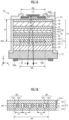
- FIG. 1A is a cross-sectional view schematically illustrating an example of a structure of a photonic-crystal surface-emitting laser element (hereinafter, also referred to as a PCSEL element) 10 according to a first embodiment of the present invention.
- a semiconductor structure layer 11 is formed on a translucent substrate 12.
- a semiconductor layer is laminated perpendicular to a central axis CX of the semiconductor structure layer 11.
- the semiconductor structure layer 11 is made of a hexagonal nitride semiconductor.
- the semiconductor structure layer 11 is made of, for example, a GaN-based semiconductor.
- the semiconductor structure layer 11 including a plurality of semiconductor layers is formed on the substrate 12, that is, an n-cladding layer (first conductivity type first cladding layer) 13, an n-side guide layer (first guide layer) 14 that is a guide layer provided on the n side, a light distribution adjustment layer 23, an active layer (ACT) 15, a p-side guide layer (second guide layer) 16 that is a guide layer provided on the p side, an electron blocking layer (EBL) 17, a p-cladding layer (second conductivity type second cladding layer) 18, and a p-contact layer 19 are formed in this order.
- first conductivity type is an n-type and the second conductivity type that is a conductivity type opposite to the first conductivity type is a p-type will be described.
- first conductivity type and the second conductivity type may be a p-type and an n-type, respectively.
- the substrate 12 is a GaN single crystal substrate with a +c-plane in which a main surface is a ⁇ 0001 ⁇ plane on which Ga atoms are arranged on the outermost surface.
- the substrate 12 is not limited to this configuration, but a just substrate, or, for example, a substrate in which a main surface is offset to about 1° in an m-axis direction is preferable.
- the substrate that is offset to about 1° in the m-axis direction can obtain mirror growth under a wide range of growth conditions.
- a substrate surface (a back surface or a light emission surface) on which a light emission region 20L opposite to the main surface is the "-c" plane that is the (000-1) plane on which N atoms are arranged on the outermost surface.
- the -c-plane is resistant to oxidation or the like, and is thus suitable as a light extraction surface.
- the n-cladding layer 13 is, for example, an n-type Al 0.04 Ga 0.96 N layer (layer thickness: 2 ⁇ m) having an Al composition of 4%.
- the n-side guide layer 14 includes a lower guide layer 14A, an air-hole layer 14P that is a photonic crystal layer (PC layer), and an embedded layer 14B.
- the n-side guide layer 14 is, for example, an n-type GaN layer (layer thickness: 360 nm).
- the lower guide layer 14A of the n-side guide layer 14 is an n-type GaN layer (layer thickness: 200 nm).
- the air-hole layer 14P has a layer thickness (or a depth of the air holes 14K) of 90 nm.
- the embedded layer 14B is an n-type GaN layer (layer thickness: 90 nm).
- the light distribution adjustment layer 23 is an undoped In 0.03 Ga 0.97 N layer (layer thickness: 50 nm).
- the light distribution adjustment layer 23 also functions as an adjustment layer for adjusting the coupling efficiency (light field) between light and the air-hole layer 14P.
- the active layer 15 that is a light-emitting layer is, for example, a multiple quantum well (MQW) layer including two quantum well layers.
- a barrier layer and the quantum well layer of the MQW are a GaN layer (layer thickness: 6.0 nm) and an InGaN layer (layer thickness: 3.0 nm), respectively.
- an emission wavelength of the active layer 15 is 435 nm.
- the p-side guide layer 16 includes a p-side guide layer (1) 16Aand a p-side guide layer (2) 16B.
- the p-side guide layer (1) 16A is an undoped In 0.02 Ga 0.98 N layer (layer thickness: 70 nm)
- the p-side guide layer (2) 16B is an undoped GaN layer (layer thickness: 180 nm).
- the p-side guide layer 16 is set to be an undoped layer in consideration of light absorption by a dopant (Mg: magnesium or the like), but may be doped to obtain excellent electrical conductivity.
- a dopant Mg: magnesium or the like
- the In composition and the layer thickness of the p-side guide layer (1) 16A can be appropriately selected.
- the electron blocking layer (EBL) 17 is an Al 0.2 Ga 0.8 N layer (layer thickness: 15 nm), and the p-cladding layer 18 is an Mg-doped p-Al 0.06 Ga 0.94 N layer (layer thickness: 290 nm).
- the p-contact layer 19 is an Mg-doped p-GaN layer (layer thickness: 25 nm).
- an "n side” and a “p side” do not necessarily mean having an n-type and a p-type.
- the n-side guide layer means a guide layer provided closer to the n side than the active layer, and may be an undoped layer (or an i layer).
- the n-cladding layer 13 may include a plurality of layers instead of a single layer. In this case, all the layers do not need to be n layers (n-doped layers), and may include an undoped layer (i layer). The same also applies to the p-side guide layer 16 and the p-cladding layer 18. In addition, it is not necessary to provide all the above-described semiconductor layers, and any configuration may be adopted as long as the configuration includes an n-type semiconductor layer, a p-type semiconductor layer, and an active layer (light-emitting layer) interposed between these layers.
- a light interference layer 31 is provided on the semiconductor structure layer 11, that is, the p-contact layer 19 (upper surface), and a light reflection layer 32 is provided on the light interference layer 31.
- a p-electrode (anode) 20B is provided on the light reflection layer 32.
- a forming region of the light interference layer 31 and the light reflection layer 32 will be referred to as an anode region RA.
- insulating film 21 such as SiO 2 .
- the insulating film 21 is formed to cover side surfaces of the light interference layer 31, the light reflection layer 32, and the p-electrode 20B and an edge portion of an upper surface of the p-electrode 20B.
- Radiated light from the active layer 15 is diffracted by the air-hole layer (PC layer) 14P.
- Light (direct diffracted light Ld: first diffracted light) diffracted by the air-hole layer 14P and directly emitted from the air-hole layer 14P, and light (reflected diffracted light Lr: second diffracted light) emitted due to diffraction of the air-hole layer 14P and reflected by the light reflection layer 32 are emitted to the outside from the light emission region 20L ( FIG. 2C ) of a back surface (emission surface) 12R of the substrate 12.
- FIG. 1B is an enlarged cross-sectional view schematically illustrating the details of the air-hole layer 14P (photonic crystal layer) of FIG. 1A and air holes arranged in the air-hole layer 14P.
- air hole pairs 14K each of which consists of a main air hole 14K1 and a secondary air hole 14K2 are two-dimensionally arranged at square lattice point positions of lattice points. That is, the air-hole layer 14P is formed as an air-hole layer having a dual lattice structure.
- the air hole pairs 14K will be simply referred to as the air holes 14K.
- the air holes 14K have a period PC, for example, in a square lattice shape on a crystal growth plane (growth plane of the semiconductor layer), that is, a plane parallel to the n-side guide layer 14, and the air holes 14K are formed to be two-dimensionally arranged at square lattice point positions, respectively and embedded in the n-side guide layer 14.
- FIG. 2A is a plan view schematically illustrating an upper surface of the PCSEL element 10
- FIG. 2B is a cross-sectional view schematically illustrating a cross-section of the air-hole layer 14P in a plane parallel to the n-side guide layer 14
- FIG. 2C is a plan view schematically illustrating a lower surface of the PCSEL element 10.
- the air holes 14K are periodically arranged and provided in, for example, a rectangular air hole forming region 14R.
- the anode region RA (the forming region of the light interference layer 31 and the light reflection layer 32) is formed to be in the air hole forming region 14R.
- an inner diameter of an n-electrode 20A may be more than or equal to that of the anode region RA when seen from a direction perpendicular to the air-hole layer 14P.
- a region inside the n-electrode 20A is the light emission region 20L.
- a bonding pad 20C that is electrically connected to the n-electrode 20 A and is connected to a wire for supplying power from the outside is provided.
- FIG. 3 is a diagram illustrating the light interference layer 31 and the light reflection layer 32 of the PCSEL element 10 according to the first embodiment and interference of diffracted light. More specifically, in FIG. 3 , the upper section schematically illustrates a cross-section of the semiconductor structure layer 11, the light interference layer 31, and the light reflection layer 32, the middle section schematically illustrates an intensity of interference light LS generated by interference, and the lower section schematically illustrates a beam shape and an intensity of the interference light LS.
- the light interference layer 31 is formed of a translucent conductor layer, for example, indium tin oxide (ITO).
- ITO indium tin oxide
- the light interference layer 31 is in ohmic contact with the p-contact layer 19.
- the light interference layer 31 is not limited to ITO and can be formed of a translucent conductor such as zinc tin oxide (ZTO).
- the light interference layer 31 has a circular shape in a top view, that is, when seen from a direction (z direction) perpendicular to the semiconductor structure layer 11.
- the light interference layer 31 consists of a light interference layer 31(1) in a central region R1 (hereinafter, also referred to as the first region) that has a circular shape and a layer thickness d1 and a light interference layer 31(2) in a peripheral region R2 (hereinafter, also referred to as the second region) that is a region outside the central region R1, has an annular shape concentric with the central region R1, and has a smaller layer thickness (layer thickness d2) than the central region R1 (d1 > d2).
- the light interference layer 31(1) and the light interference layer 31(2) will also be referred to as the first region layer and the second region layer, respectively.
- a diameter of the central region R1 is 100 ⁇ m
- a diameter (outer diameter) of the peripheral region R2 is 300 ⁇ m (that is, an inner diameter is 100 ⁇ m).
- the diameters of the central region R1 and the peripheral region R2 can be appropriately set from the viewpoint of beam (transverse mode) control.
- a metal layer is formed as the light reflection layer 32 on the light interference layer 31.
- the p-electrode 20B provided on the light reflection layer 32 is not illustrated.
- the light reflection layer 32 reflects diffracted light from the air-hole layer 14P.
- the light reflection layer 32 is formed to cover the entire surface of the light interference layer 31.
- the light reflection layer 32 for example, silver (Ag) having a high reflectivity of 85% or palladium (Pd) having a reflectivity of 45% can be used.
- the layer thickness of the light reflection layer 32 is, for example, 200 nm, but is not limited thereto.
- the p-electrode 20B provided on the light reflection layer 32 (refer to FIG. 1A ) consists of, for example, Ti/Pt/Au, but is not limited thereto.
- As the p-electrode 20B for example, Ti/Au, Ti/Al/Ti/Pt/Au, or Ni/Pt/Au can be used.
- the layer thickness of the p-electrode 20B may be increased to function as a pad electrode.
- each of the semiconductor layers other than the air-hole layer 14P and the active layer 15 is not illustrated to clarify the drawing.
- a distance between a diffraction surface WS of the air-hole layer 14P and an interface of the semiconductor structure layer 11 and the light interference layer 31 is represented by d.
- the interference of the diffracted light in the PCSEL element 10 will be described below.
- the radiated light of the active layer 15 is diffracted by the air-hole layer 14P.
- the light (reflected diffracted light Lr) that is reflected by the light reflection layer 32 through the light interference layer 31(1) of the central region R1 interferes with the direct diffracted light Ld from the air-hole layer 14P such that interference light (combined light) LS1 is generated (interference light of the first region).
- the reflected diffracted light Lr transmitted through the light interference layer 31(2) of the peripheral region R2 interferes with the direct diffracted light Ld from the air-hole layer 14P such that interference light LS2 is generated (interference light of the second region).
- a layer thickness d1 of the light interference layer 31(1) in the central region R1 is determined such that the direct diffracted light Ld and the reflected diffracted light Lr weaken each other.
- a layer thickness d2 of the light interference layer 31(2) in the peripheral region R2 is determined such that the direct diffracted light Ld and the reflected diffracted light Lr strengthen each other.
- intensities of the interference light LS1 and the interference light LS2 that are generated in the central region (first region) R1 and the peripheral region (second region) R2 and emitted satisfy LS1 ⁇ LS2. That is, the peripheral region R2 is a region brighter than the central region R1.
- the intensities of the interference light LS1 and the interference light LS2 will be described as the interference light intensity LS1 and the interference light intensity LS2 using the same reference numerals, respectively.
- the interference light LS1 and the interference light LS2 do not need to be distinguished from each other, the interference light LS1 and the interference light LS2 will be collectively referred to as the interference light LS.
- the air-hole layer (photonic crystal layer) 14P when the air-hole layer (photonic crystal layer) 14P is on an xy plane, light propagating in the air-hole layer 14P forms a standing wave in the xy plane, and a part of the light is diffracted by the photonic crystal in the z-axis direction orthogonal to the xy plane and emitted as laser light.
- Reflection surfaces SR1 and SR2 (hereinafter, referred to as the reflection surface SR when they do not need to be distinguished from each other) of the light reflection layer 32 in the central region R1 and the peripheral region R2 are on a plane parallel to the air-hole layer 14P, and laser light diffracted by the air-hole layer 14P and the reflection surface SR are orthogonal to each other.
- a resonator loss in the PCSEL element 10 is divided into a loss component ⁇ p in a direction in the same plane (in the xy plane) as the air-hole layer 14P and a loss component ⁇ v in a perpendicular direction (z direction) orthogonal to the air-hole layer 14P.
- the component ⁇ v in the perpendicular direction contributes to laser emission.
- the reflection surface SR it is necessary to consider absorption and reflection on the reflection surface SR to consider the emission efficiency.
- the loss ⁇ p in the in-plane direction, the loss ⁇ v in the perpendicular direction, and the slope efficiency ⁇ SE are represented by as follows. ⁇ // , ⁇ v , ⁇ SE
- the component radiated in the perpendicular direction by diffraction is ⁇ v. Therefore, assuming that diffraction occurs uniformly in the vertical direction ( ⁇ z direction) of the z-axis, the energy emitted in the ⁇ z direction is the same, and thus the laser light radiated in the ⁇ z direction is 0.5 ⁇ v.
- the loss absorbed by the reflection surface SR is 0.5 ⁇ v(1 - R).
- ⁇ i is an injection efficiency during a laser oscillation operation.
- an internal loss ⁇ i by material absorption is considered.
- ⁇ v/ ⁇ p when ⁇ v/ ⁇ p is about 20 or more, the slope efficiency ⁇ SE is saturated. Accordingly, from the viewpoint of increasing the slope efficiency ⁇ SE, ⁇ v is preferably about 20 times ⁇ p.
- the slope efficiency ⁇ SE is normalized with the slope efficiency where there is no reflection.
- the slope efficiency changes in a cos-shaped curve depending on the phase difference ⁇ . That is, a region (hereinafter, referred to as the strengthening region) where the radiation intensity is relatively strong and a region where the radiation intensity is relatively weak periodically appears at an interval of 2 ⁇ .
- an element region (hereinafter, referred to as the strengthening region) where the direct diffracted light Ld and the reflected diffracted light Lr strengthen each other in the perpendicular direction of the air-hole layer and an element region (hereinafter, referred to as the weakening region) where the direct diffracted light Ld and the reflected diffracted light Lr weaken each other are different from those of another light-emitting device such as a vertical cavity laser.
- the range of the phase difference ⁇ in the strengthening region is wide, and the range of the phase difference ⁇ in the weakening region is narrow.
- the layer thickness allowable range of the interference layer of the strengthening region is wide, the film thickness control is facilitated, and the emission intensity can be controlled.
- the ranges of the phase differences ⁇ in the strengthening region and the weakening region of the PCSEL element vary depending on the reflectivity of the reflection layer.
- the allowable width of the layer thickness range of the interference layer of the weakening region is narrow.
- the allowable width of the layer thickness range of the weakening region is widened, and the control of the emission intensity is facilitated as in the strengthening region.
- a radiated wave profile radiated in a direction perpendicular to the air-hole layer 14P in the PCSEL element 10 according to the first embodiment is calculated.
- Non-Patent Literature 1 light propagating in the xy direction (in-plane direction) of the air-hole layer 14P, the wave source (diffraction surface) of the diffracted wave by the air-hole layer 14P, and the radiated wave radiated in the perpendicular direction by diffraction can be calculated using a coupled wave theory.
- FIG. 6 is a diagram illustrating a calculation result of an electric field amplitude of a radiated wave when light propagating in the air-hole layer 14P in the x-axis direction is diffracted by the air-hole layer 14P and radiated in a perpendicular direction ( ⁇ z direction).
- the air hole filling factor FF is 10%.
- the air holes 14K of the air-hole layer 14P are assumed to have a hexagonal columnar structure having a central axis extending in the z-axis direction, and the calculation is performed.
- the air hole period PC is 176 nm.
- the light diffracted by the air-hole layer 14P is radiated, as radiated light, symmetrically in the +z-axis direction and the -z-axis direction at a certain point (a point on the z-axis) as a starting point in the air-hole layer 14P.
- the point is the diffraction surface (wave source) WS in the device.
- the same reference numerals are used and the surface is described as the diffraction surface WS.
- a symmetrical center surface of an electric field amplitude when the light standing in the air-hole layer 14P is diffracted symmetrically in a direction orthogonal to the air-hole layer 14P is the diffraction surface WS.
- An electric field profile in a fundamental mode changes depending on the lattice structure (a single lattice structure or a multi-lattice structure) of the air-hole layer. Therefore, the position of the diffraction surface WS changes depending on the lattice structure of the air-hole layer.
- a separation distance dr between the diffraction surface WS and the reflection surface SR can be represented by Expression (2.1) below.
- Expression (2.1) can be derived from Expression (2.2) below.
- kx ⁇ 360 2 ⁇ + ⁇ + 2 m ⁇
- k 2 ⁇ ⁇
- x 2 n ave dr
- the film thickness of the light interference layer 31 can be calculated.
- phase difference ⁇ satisfying ⁇ SE(R) ⁇ ⁇ SE(0) is given by Expression (2.5) below.
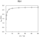
- FIG. 7 is a diagram illustrating a relationship between the slope efficiency ⁇ SE to the phase difference ⁇ and an interference layer film thickness.
- a range of the phase difference ⁇ where the direct diffracted light Ld and the reflected diffracted light Lr weaken each other, that is, a range of the phase difference ⁇ where the normalized slope efficiency is lower than 1 is illustrated as a phase difference range WI.
- a phase difference range other than the phase difference range WI is the strengthening range.
- the slope efficiency is more preferably higher than 1.
- the interference layer film thickness (indicated by a one-dot chain line) is obtained by subtracting the distance d from the separation distance dr.
- the weakening range and the strengthening range are represented by Expression (2.6) below due to the phase difference ( ⁇ ) dependence of the slope efficiency ⁇ SE and the interference layer film thickness illustrated in FIG. 7 .
- a separation distance dr from a wave source WS to the reflection surface SR when the phase difference ⁇ is in the above range is obtained.
- the peripheral region R2 can be set to be brighter than the central region R1 (interference light intensity: LS1 ⁇ LS2), and beam control can be performed.
- the layer thickness d2 of the strengthening region is less than the layer thickness d1 of the weakening region (central region R1). This is because, while suppressing a reduction in emission intensity caused by the material loss of the light interference layer 31(2) in the strengthening region, laser light having a desired beam shape can be obtained.
- the light interference layer 31 has a convex structure where the central region R1 is thicker than the peripheral region R2.
- FIG. 8 is a schematic cross-sectional view illustrating a modification example of the first embodiment.
- the layer thickness d2 of the strengthening region (peripheral region R2) is more than the layer thickness d1 of the weakening region (central region R1).
- the light interference layer 31 has a concave structure where the peripheral region R2 is thicker than the central region R1. Even in this case, it is possible to realize a photonic-crystal surface-emitting laser where a beam shape can be accurately controlled and beam (transverse mode) stability is excellent up to a high output.
- FIG. 9 is a diagram schematically illustrating a cross-section of a PCSEL element 50 according to a second embodiment, an interference light intensity, and a beam shape.
- a light reflection layer 32(1) is formed on the light interference layer 31(1)
- a light reflection layer 32(2) having a different reflectivity from the light reflection layer 32(1) is formed on the light interference layer 31(2).
- Other points are the same as those of the PCSEL element 10 according to the first embodiment.
- the light interference layers 31(1) and 31(2) are ITO layers
- the central region R1 is the weakening region
- the peripheral region R2 is the strengthening region. Accordingly, the intensities of the interference light LS1 and the interference light LS2 in the central region R1 and the peripheral region R2 satisfy LS1 ⁇ LS2. That is, the light reflection layer 32(1) having a relatively low reflectivity is applied to the weakening region where the intensities of the interference light weaken each other, and the light reflection layer 32(2) having a relatively high reflectivity is applied to the strengthening region where the intensities of the interference light strengthen each other.
- the layer thickness d1 of the weakening region (central region R1) is obtained by calculating the separation distance dr of Expression (2.1) in the range of each of the phase differences ⁇ of Expression (2.10) and subtracting the distance d between the diffraction surface WS and the light interference layer 31 from the separation distance dr.
- the light reflection layer 32(2) that is an Ag layer is applied to the strengthening region (peripheral region R2) according to the second embodiment. Therefore, the film thickness d2 is obtained as in Expression (2.9).
- the peripheral region R2 can be set to be brighter than the central region R1 (interference light intensity: LS1 ⁇ LS2), and beam control can be performed.
- the layer thickness d2 of the strengthening region is less than the layer thickness d1 of the weakening region (central region R1). This is because, while suppressing a reduction in emission intensity caused by the material loss of the light interference layer 31(2) in the strengthening region, laser light having a desired beam shape can be obtained.
- the minimum value of 104.8 nm of Expression (2.11) is adopted as the layer thickness d1 of the weakening region (central region R1) and the minimum value of 72.8 nm of Expression (2.11) is adopted as the layer thickness d2 of the strengthening region (peripheral region R2).
- the light interference layer 31 is divided into a first region R1, a second region R2, ..., and an n-th region Rn (n represents an integer of 3 or more) in order from the center.
- the light interference layer 31 includes the light interference layer 31(1), the light interference layer 31(2), ..., and the light interference layer 31(n).
- the light interference layer 31(1) is provided in the first region R1 as the central region, and the light interference layers 31(2), 31(3), ..., and 31(n) are provided in the peripheral region in this order from the side outside the first region R1.
- FIG. 11 is a diagram schematically illustrating a cross-section of a PCSEL element 60 according to the third embodiment, an interference light intensity, and a beam shape.
- the light interference layer 31 consists of the light interference layer 31(1), the light interference layer 31(2), and a light interference layer 31(3) in order from the center.
- the light reflection layer 32 is provided on the light interference layer 31.
- the diameters of the first region R1, the second region R2, and the third region R3 are 100 ⁇ m, 200 ⁇ m, and 300 ⁇ m, respectively.
- the interference light intensity LS1 of the first region R1 (central region) is the highest, the interference light intensity LS2 of the second region R2 is the lowest, and an interference light intensity LS3 of the third region R3 is the intermediate intensity between the first region R1 and the second region R2.
- the layer thicknesses of the light interference layer 31(1), the light interference layer 31(2), and the light interference layer 31(3) are determined such that LS1 > LS3 > LS2 is satisfied.
- the layer thickness of each of the light interference layers can be determined based on the phase difference ( ⁇ ) dependence of the interference layer thickness described in the first embodiment and the second embodiment.
- the layer thicknesses of the ITO layers of the light interference layer 31(1), the light interference layer 31(2), and the light interference layer 31(3) are 73 nm, 118 nm, and 103 nm, respectively.
- the present embodiment is the same as the above-described embodiments in that it is possible to provide a photonic-crystal surface-emitting laser where a beam shape can be easily and accurately controlled and beam (transverse mode) stability is excellent up to a high output.
- the second region R2 is provided between the first region R1 and the third region R3 that are regions having high interference light intensities, the second region R2 having a lower interference light intensity than the first region R1 and the third region R3. That is, the regions R1 and R3 having high interference light intensities can be provided to be separated from each other.
- a heating position and a heating process can be adjusted.
- preheating of a processing object using light of the region R3 that is previously irradiated in a propagation direction of the light beam can be performed, subsequently main processing using light of the region R1 can be performed, and subsequently annealing after processing using light of the region R3 can be performed.
- this configuration has an advantageous effect in that the quality of welding can be improved and the post-processes can also be performed at once.
- the light interference layer 31 consists of three regions. In general, the same can apply to a case where the light interference layer 31 consists of the first region R1, the second region R2, ..., and the n-th region Rn.
- the light reflection layers 32(1) and 32(2) having different reflectivities may be applied.
- the term "circular shape” includes an elliptical shape and an oval shape
- the term “annular shape” includes an elliptical annular shape and an oval elliptical shape.
- the light interference layer is not limited to a circular shape, and may have a shape such as a rectangular shape or a polygonal shape. It is preferable that the regions of the light interference layer have similar shapes concentric with each other.
- dielectrics, reflective metals, and compositions, numerical values, and the like thereof in the above-described embodiments are merely exemplary, and appropriate modifications can be applied within the scope of the present invention.
- the PCSEL elements having the single lattice structure or the dual lattice structure have been described.
- the present invention is also applicable to a general PCSEL element having a multi-lattice structure.
- the present invention exemplifies the air-hole layer in which the air hole has a hexagonal columnar shape, but also can be applied to a case where the air hole has a columnar shape, a rectangular shape, a polygonal shape, or an irregular columnar shape such as a teardrop shape.
Landscapes
- Physics & Mathematics (AREA)
- Condensed Matter Physics & Semiconductors (AREA)
- General Physics & Mathematics (AREA)
- Electromagnetism (AREA)
- Optics & Photonics (AREA)
- Semiconductor Lasers (AREA)
- Led Devices (AREA)
Applications Claiming Priority (2)
| Application Number | Priority Date | Filing Date | Title |
|---|---|---|---|
| JP2022051401A JP7738854B2 (ja) | 2022-03-28 | 2022-03-28 | 面発光レーザ素子 |
| PCT/JP2023/009788 WO2023189523A1 (ja) | 2022-03-28 | 2023-03-14 | 面発光レーザ素子 |
Publications (2)
| Publication Number | Publication Date |
|---|---|
| EP4481963A1 true EP4481963A1 (de) | 2024-12-25 |
| EP4481963A4 EP4481963A4 (de) | 2025-06-25 |
Family
ID=88200964
Family Applications (1)
| Application Number | Title | Priority Date | Filing Date |
|---|---|---|---|
| EP23779543.0A Pending EP4481963A4 (de) | 2022-03-28 | 2023-03-14 | Oberflächenemittierendes laserelement |
Country Status (5)
| Country | Link |
|---|---|
| US (1) | US20250047067A1 (de) |
| EP (1) | EP4481963A4 (de) |
| JP (1) | JP7738854B2 (de) |
| CN (1) | CN118901170A (de) |
| WO (1) | WO2023189523A1 (de) |
Cited By (1)
| Publication number | Priority date | Publication date | Assignee | Title |
|---|---|---|---|---|
| EP4521568A4 (de) * | 2022-06-14 | 2025-09-03 | Univ Kyoto | Oberflächenemittierendes laserelement |
Families Citing this family (2)
| Publication number | Priority date | Publication date | Assignee | Title |
|---|---|---|---|---|
| JP2026010494A (ja) * | 2024-07-09 | 2026-01-22 | 住友電気工業株式会社 | フォトニック結晶面発光レーザ |
| CN121035771B (zh) * | 2025-10-28 | 2026-02-27 | 苏州实验室 | 一种衍射型面发射半导体激光器 |
Family Cites Families (7)
| Publication number | Priority date | Publication date | Assignee | Title |
|---|---|---|---|---|
| WO2016001702A1 (en) | 2014-07-03 | 2016-01-07 | Arcelormittal | Method for producing a high strength coated steel sheet having improved strength, ductility and formability |
| EP3588704B1 (de) | 2017-02-27 | 2022-07-13 | Kyoto University | Oberflächenemittierender laser und verfahren zur herstellung eines oberflächenemittierenden lasers |
| JP7219552B2 (ja) * | 2018-05-15 | 2023-02-08 | 浜松ホトニクス株式会社 | 発光デバイス |
| JP7212882B2 (ja) | 2018-05-24 | 2023-01-26 | スタンレー電気株式会社 | 垂直共振器型発光素子 |
| US10340659B1 (en) * | 2018-06-14 | 2019-07-02 | Conary Enterprise Co., Ltd. | Electronically pumped surface-emitting photonic crystal laser |
| CN115298916B (zh) * | 2020-03-16 | 2025-07-11 | 国立大学法人京都大学 | 面发射激光元件及面发射激光元件的制造方法 |
| JP7485284B2 (ja) * | 2020-07-14 | 2024-05-16 | 国立大学法人京都大学 | フォトニック結晶面発光レーザ素子 |
-
2022
- 2022-03-28 JP JP2022051401A patent/JP7738854B2/ja active Active
-
2023
- 2023-03-14 CN CN202380029114.6A patent/CN118901170A/zh active Pending
- 2023-03-14 WO PCT/JP2023/009788 patent/WO2023189523A1/ja not_active Ceased
- 2023-03-14 US US18/847,844 patent/US20250047067A1/en active Pending
- 2023-03-14 EP EP23779543.0A patent/EP4481963A4/de active Pending
Cited By (1)
| Publication number | Priority date | Publication date | Assignee | Title |
|---|---|---|---|---|
| EP4521568A4 (de) * | 2022-06-14 | 2025-09-03 | Univ Kyoto | Oberflächenemittierendes laserelement |
Also Published As
| Publication number | Publication date |
|---|---|
| EP4481963A4 (de) | 2025-06-25 |
| WO2023189523A1 (ja) | 2023-10-05 |
| JP7738854B2 (ja) | 2025-09-16 |
| JP2023144431A (ja) | 2023-10-11 |
| CN118901170A (zh) | 2024-11-05 |
| US20250047067A1 (en) | 2025-02-06 |
Similar Documents
| Publication | Publication Date | Title |
|---|---|---|
| EP4481963A1 (de) | Oberflächenemittierendes laserelement | |
| Knauer et al. | High-power 808 nm lasers with a super-large optical cavity | |
| US8831061B2 (en) | Edge emitting semiconductor laser chip | |
| US20050040410A1 (en) | Tilted cavity semiconductor optoelectronic device and method of making same | |
| EP3611811A1 (de) | Lichtemittierendes element und lichtemittierende vorrichtung | |
| US20190363515A1 (en) | Vertical cavity light-emitting element | |
| US12068581B2 (en) | Surface-emitting semiconductor laser | |
| US20230387659A1 (en) | Method of manufacturing surface-emitting laser element | |
| KR20070065231A (ko) | 면 발광 레이저 | |
| US20250385486A1 (en) | Photonic-crystal surface-light-emitting laser element | |
| US20250055259A1 (en) | Surface-emitting laser element | |
| US12407146B2 (en) | Vertical cavity light-emitting element and manufacturing method of the same | |
| TWI830021B (zh) | 光子晶體面射型雷射 | |
| US20250364784A1 (en) | Surface-emitting laser element | |
| US10516251B2 (en) | Reliable high-speed oxide-confined vertical-cavity surface-emitting laser | |
| US20250210940A1 (en) | Semiconductor laser element | |
| US20250392103A1 (en) | Vertical cavity light-emitting element | |
| JP2012104764A (ja) | 半導体発光素子 | |
| WO2025258311A1 (ja) | 半導体レーザ素子 | |
| CN113725726A (zh) | 外腔式vcsel激光器、vcsel阵列和激光器的制备方法 | |
| JP2006019473A (ja) | 半導体レーザ |
Legal Events
| Date | Code | Title | Description |
|---|---|---|---|
| STAA | Information on the status of an ep patent application or granted ep patent |
Free format text: STATUS: THE INTERNATIONAL PUBLICATION HAS BEEN MADE |
|
| PUAI | Public reference made under article 153(3) epc to a published international application that has entered the european phase |
Free format text: ORIGINAL CODE: 0009012 |
|
| STAA | Information on the status of an ep patent application or granted ep patent |
Free format text: STATUS: REQUEST FOR EXAMINATION WAS MADE |
|
| 17P | Request for examination filed |
Effective date: 20240918 |
|
| AK | Designated contracting states |
Kind code of ref document: A1 Designated state(s): AL AT BE BG CH CY CZ DE DK EE ES FI FR GB GR HR HU IE IS IT LI LT LU LV MC ME MK MT NL NO PL PT RO RS SE SI SK SM TR |
|
| STAA | Information on the status of an ep patent application or granted ep patent |
Free format text: STATUS: EXAMINATION IS IN PROGRESS |
|
| A4 | Supplementary search report drawn up and despatched |
Effective date: 20250523 |
|
| RIC1 | Information provided on ipc code assigned before grant |
Ipc: H01S 5/343 20060101ALN20250519BHEP Ipc: H01S 5/185 20210101ALI20250519BHEP Ipc: H01S 5/11 20210101AFI20250519BHEP |
|
| DAV | Request for validation of the european patent (deleted) | ||
| DAX | Request for extension of the european patent (deleted) | ||
| 17Q | First examination report despatched |
Effective date: 20250604 |