EP4481834B1 - Solar cell and method for producing the solar cell - Google Patents
Solar cell and method for producing the solar cell Download PDFInfo
- Publication number
- EP4481834B1 EP4481834B1 EP23208472.3A EP23208472A EP4481834B1 EP 4481834 B1 EP4481834 B1 EP 4481834B1 EP 23208472 A EP23208472 A EP 23208472A EP 4481834 B1 EP4481834 B1 EP 4481834B1
- Authority
- EP
- European Patent Office
- Prior art keywords
- doped polysilicon
- layer
- barrier layer
- substrate
- polysilicon layer
- Prior art date
- Legal status (The legal status is an assumption and is not a legal conclusion. Google has not performed a legal analysis and makes no representation as to the accuracy of the status listed.)
- Active
Links
Images


Classifications
-
- H—ELECTRICITY
- H10—SEMICONDUCTOR DEVICES; ELECTRIC SOLID-STATE DEVICES NOT OTHERWISE PROVIDED FOR
- H10F—INORGANIC SEMICONDUCTOR DEVICES SENSITIVE TO INFRARED RADIATION, LIGHT, ELECTROMAGNETIC RADIATION OF SHORTER WAVELENGTH OR CORPUSCULAR RADIATION
- H10F77/00—Constructional details of devices covered by this subclass
- H10F77/30—Coatings
- H10F77/306—Coatings for devices having potential barriers
- H10F77/311—Coatings for devices having potential barriers for photovoltaic cells
-
- H—ELECTRICITY
- H10—SEMICONDUCTOR DEVICES; ELECTRIC SOLID-STATE DEVICES NOT OTHERWISE PROVIDED FOR
- H10F—INORGANIC SEMICONDUCTOR DEVICES SENSITIVE TO INFRARED RADIATION, LIGHT, ELECTROMAGNETIC RADIATION OF SHORTER WAVELENGTH OR CORPUSCULAR RADIATION
- H10F10/00—Individual photovoltaic cells, e.g. solar cells
- H10F10/10—Individual photovoltaic cells, e.g. solar cells having potential barriers
- H10F10/16—Photovoltaic cells having only PN heterojunction potential barriers
- H10F10/164—Photovoltaic cells having only PN heterojunction potential barriers comprising heterojunctions with Group IV materials, e.g. ITO/Si or GaAs/SiGe photovoltaic cells
- H10F10/165—Photovoltaic cells having only PN heterojunction potential barriers comprising heterojunctions with Group IV materials, e.g. ITO/Si or GaAs/SiGe photovoltaic cells the heterojunctions being Group IV-IV heterojunctions, e.g. Si/Ge, SiGe/Si or Si/SiC photovoltaic cells
- H10F10/166—Photovoltaic cells having only PN heterojunction potential barriers comprising heterojunctions with Group IV materials, e.g. ITO/Si or GaAs/SiGe photovoltaic cells the heterojunctions being Group IV-IV heterojunctions, e.g. Si/Ge, SiGe/Si or Si/SiC photovoltaic cells the Group IV-IV heterojunctions being heterojunctions of crystalline and amorphous materials, e.g. silicon heterojunction [SHJ] photovoltaic cells
-
- H—ELECTRICITY
- H10—SEMICONDUCTOR DEVICES; ELECTRIC SOLID-STATE DEVICES NOT OTHERWISE PROVIDED FOR
- H10F—INORGANIC SEMICONDUCTOR DEVICES SENSITIVE TO INFRARED RADIATION, LIGHT, ELECTROMAGNETIC RADIATION OF SHORTER WAVELENGTH OR CORPUSCULAR RADIATION
- H10F71/00—Manufacture or treatment of devices covered by this subclass
- H10F71/121—The active layers comprising only Group IV materials
-
- H—ELECTRICITY
- H10—SEMICONDUCTOR DEVICES; ELECTRIC SOLID-STATE DEVICES NOT OTHERWISE PROVIDED FOR
- H10F—INORGANIC SEMICONDUCTOR DEVICES SENSITIVE TO INFRARED RADIATION, LIGHT, ELECTROMAGNETIC RADIATION OF SHORTER WAVELENGTH OR CORPUSCULAR RADIATION
- H10F71/00—Manufacture or treatment of devices covered by this subclass
- H10F71/121—The active layers comprising only Group IV materials
- H10F71/1221—The active layers comprising only Group IV materials comprising polycrystalline silicon
-
- H—ELECTRICITY
- H10—SEMICONDUCTOR DEVICES; ELECTRIC SOLID-STATE DEVICES NOT OTHERWISE PROVIDED FOR
- H10F—INORGANIC SEMICONDUCTOR DEVICES SENSITIVE TO INFRARED RADIATION, LIGHT, ELECTROMAGNETIC RADIATION OF SHORTER WAVELENGTH OR CORPUSCULAR RADIATION
- H10F77/00—Constructional details of devices covered by this subclass
- H10F77/10—Semiconductor bodies
- H10F77/16—Material structures, e.g. crystalline structures, film structures or crystal plane orientations
- H10F77/162—Non-monocrystalline materials, e.g. semiconductor particles embedded in insulating materials
- H10F77/164—Polycrystalline semiconductors
- H10F77/1642—Polycrystalline semiconductors including only Group IV materials
-
- H—ELECTRICITY
- H10—SEMICONDUCTOR DEVICES; ELECTRIC SOLID-STATE DEVICES NOT OTHERWISE PROVIDED FOR
- H10F—INORGANIC SEMICONDUCTOR DEVICES SENSITIVE TO INFRARED RADIATION, LIGHT, ELECTROMAGNETIC RADIATION OF SHORTER WAVELENGTH OR CORPUSCULAR RADIATION
- H10F77/00—Constructional details of devices covered by this subclass
- H10F77/20—Electrodes
- H10F77/206—Electrodes for devices having potential barriers
- H10F77/211—Electrodes for devices having potential barriers for photovoltaic cells
-
- Y—GENERAL TAGGING OF NEW TECHNOLOGICAL DEVELOPMENTS; GENERAL TAGGING OF CROSS-SECTIONAL TECHNOLOGIES SPANNING OVER SEVERAL SECTIONS OF THE IPC; TECHNICAL SUBJECTS COVERED BY FORMER USPC CROSS-REFERENCE ART COLLECTIONS [XRACs] AND DIGESTS
- Y02—TECHNOLOGIES OR APPLICATIONS FOR MITIGATION OR ADAPTATION AGAINST CLIMATE CHANGE
- Y02P—CLIMATE CHANGE MITIGATION TECHNOLOGIES IN THE PRODUCTION OR PROCESSING OF GOODS
- Y02P70/00—Climate change mitigation technologies in the production process for final industrial or consumer products
- Y02P70/50—Manufacturing or production processes characterised by the final manufactured product
Definitions
- the invention relates to the field of photovoltaic, and specifically relates to a solar cell and a method for producing the solar cell.
- the solar cell includes a tunnel oxide layer and a doped polysilicon layer.
- the tunnel oxide layer can selectively transport carriers, and the doped polysilicon layer acts as field passivation.
- the electrodes of the solar cell penetrate a functional layer (such as an anti-reflection layer) located in the electrode region and contact the doped polysilicon layer.
- the doped polysilicon layer in the solar cell has optical parasitic effects, which results in a decrease in the solar cell's utilization of incident light. Reducing the thickness of the doped polysilicon layer can reduce the absorption of incident light by the doped polysilicon layer, thereby improving the solar cell's utilization of incident light. However, the reduction in the thickness of the doped polysilicon layer increases the risk of the electrode burning through the polysilicon layer, which would result in contact between the electrode and the substrate. Contact between the electrode and the substrate will cause the recombination current density to increase, which will seriously affect the efficiency of the solar cell.
- CN 114784148 A describes a preparation method of a solar cell, the solar cell and a photovoltaic module.
- Some embodiments of the present disclosure are intended to provide a solar cell and a method for producing the solar cell that can reduce the thickness of the doped polysilicon layer while preventing the electrode from burning through the doped polysilicon layer.
- the invention provides the solar cell according to claim 1 and the method for producing a solar cell according to claim 9.
- a solar cell comprising: a substrate having a first surface and a second surfaces opposite to each other in a first direction, the first direction is a thickness direction of the substrate; a tunnel oxide layer located on the first surface and/or the second surface; a doped polysilicon layer located on a surface of the tunnel oxide layer away from the substrate; a barrier layer located in an electrode region of the solar cell and in contact with the doped polysilicon layer, a doping type of the barrier layer is the same as the doped polysilicon layer; and an electrode located in the electrode region and in contact with the barrier layer; wherein a method of forming the barrier layer includes etching the doped polysilicon layer in the electrode region in the first direction to form a groove with a predetermined depth, and forming the barrier layer in the groove, the predetermined depth is equal to or less than a thickness of the doped polysilicon layer, a material of the barrier layer includes silicon carbide and/or zinc oxide.
- the barrier layer goes deep into the doped polysilicon layer to the predetermined depth in the first direction.
- the barrier layer is located on the surface of the tunnel oxide layer away from the substrate.
- a surface of the barrier layer away from the substrate is flush with a surface of the doped polysilicon layer away from the substrate, or the surface of the barrier layer away from the substrate is closer to the substrate than the surface of the doped polysilicon layer away from the substrate, or the surface of the barrier layer away from the substrate is further away the substrate than the surface of the doped polysilicon layer away from the substrate.
- a recombination current density of the electrode region is equal to or less than 100 fA/cm 2 .
- the solar cell further comprises a dielectric layer, the dielectric layer is located on a surface of the doped polysilicon layer away from the substrate and a surface of the barrier layer away from the substrate.
- the electrode penetrates the dielectric layer and contacts the barrier layer.
- the thickness of the doped polysilicon layer is equal to or greater than 3nm, and equal to or less than 200nm.
- Some embodiments further provide a method for producing a solar cell, comprising: providing a substrate having a first surface and a second surfaces opposite to each other in a first direction, the first direction is a thickness direction of the substrate; forming a tunnel oxide layer on the first surface and/or the second surface; forming a doped polysilicon layer on a surface of the tunnel oxide layer away from the substrate; forming a barrier layer in an electrode region of the solar cell, the barrier layer is in contact with the doped polysilicon layer, and a doping type of the barrier layer is the same as the doped polysilicon layer; and forming an electrode in contact with the barrier layer; wherein a method of forming the barrier layer includes etching the doped polysilicon layer in the electrode region in the first direction to form a groove with a predetermined depth, and forming the barrier layer in the groove, the predetermined depth is equal to or less than a thickness of the doped polysilicon layer, and a material of the barrier layer includes silicon carbide and/or zinc oxide.
- a method of forming the barrier layer includes: cleaning a surface of the doped polysilicon layer; and forming the barrier layer in the electrode region, the barrier layer is in contact with a surface of the doped polysilicon layer away from the substrate.
- the recombination current density of the electrode region is equal to or less than 100fA/cm 2 .
- the thickness of the doped polysilicon layer is equal to or greater than 3nm, and equal to or less than 200nm.
- the solar cell and the producing method thereof of the present disclosure provide the barrier layer in contact with the doped polysilicon layer in the electrode region, which reduces the risk of the electrode burning through the doped polysilicon layer.
- the thickness of the doped polysilicon can be further reduced, thereby reducing the absorption of incident light by the doped polysilicon layer and improving the utilization rate of incident light by the solar cell.
- Substrate 110 first surface 111, second surface 112, tunnel oxide layer 120, doped polysilicon layer 130, initial barrier layer 132, surface 131, barrier layer 140, bottom surface 141, top surface 142, first side surface 143. Second side 144, electrode 150, electrode region 160, dielectric layer 170, and groove 180.
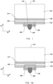
- FIG. 1 is a schematic front view of a solar cell according to an embodiment not forming part of the claimed invention but useful for the understanding thereof.
- a solar cell includes a substrate 110, a tunnel oxide layer 120, a doped polysilicon layer 130, a barrier layer 140, and an electrode 150.
- the substrate 110 has a first surface 111 and a second surface 112 opposite in the first direction D1 (which is also a thickness direction of the substrate 110).
- the first surface 111 and the second surface 112 may be polished or have a pyramid-textured topography.
- the tunnel oxide layer 120 is disposed on the first surface 111, and the doped polysilicon layer 130 is disposed on a surface of the tunnel oxide layer 120 away from the substrate 110 in the first direction D1.
- tunnel oxide layer 120 and the doped polysilicon layer 130 together form a tunnel oxide layer-doped polysilicon layer passivation structure. It should be noted that in some other embodiments, the tunnel oxide layer 120 can also be formed on the second surface 112, or formed on both the first surface 111 and the second surface 112.
- the substrate 110 may be a silicon substrate, for example, a single crystal silicon substrate or a polycrystalline silicon substrate.
- the substrate 110 may be doped, such as N-type doping and P-type doping.
- the material of the tunnel oxide layer 120 may be silicon oxide (SiO x ), and the thickness of the tunnel oxide layer 120 may be any value from 1nm to 3nm, for example, 1nm, 1.5nm, 2nm, 2.5nm, or 3nm.
- the tunnel oxide layer 120 has a selective collection effect on carriers.
- the material of the doped polysilicon layer 130 can be selected from polysilicon, and the present disclosure does not limit the grain size of the polysilicon.
- the doping type of the doped polysilicon layer 130 may be the same as that of the substrate 110, or may be opposite to that of the substrate 110.
- the solar cell has an electrode region, which is identified in FIG. 1 using a dashed rectangular frame 160.
- the electrodes of the solar cell are located in the electrode region. The electrodes are used to collect the electrical energy generated by the solar cell and transmit the electrical energy to the outside.
- the barrier layer 140 is disposed in the electrode region, and is in contact with the doped polysilicon layer 130.
- the doping type of the barrier layer 140 is the same as the doping type of the doped polysilicon layer 130.
- the doping type of the doped polysilicon layer 130 and the doping type of the barrier layer 140 are both N-type, and the corresponding doping elements can be selected from phosphorus (P), bismuth (Bi), antimony (Sb), arsenic (As), and other V group elements.
- the doping type of the doped polysilicon layer 130 and the doping type of the barrier layer 140 can also be P-type, and the corresponding doping elements can be selected from one or more III group elements such as boron (B), aluminum (Al), gallium (Ga), or indium (In).
- the electrode 150 is in contact with the barrier layer 140. It should be understood that the number of the electrode regions and the electrodes 150 in the solar cell is not limited to the one shown in FIG. 1 .
- the solar cell includes a certain number of electrode regions and electrodes 150 spaced apart in the second direction D2, which are not shown in FIG. 1 due to the limited size of FIG. 1 .
- the solar cell further includes a dielectric layer 170.
- the dielectric layer 170 is disposed on the surface of the doped polysilicon layer 130 and the barrier layer 140 away from the substrate 110 in the first direction D1. In other words, the dielectric layer 170 covers the exposed surfaces of the doped polysilicon layer 130 and the barrier layer 140.
- the electrode 150 penetrates the dielectric layer 170 and contacts the barrier layer 140.
- the dielectric layer 170 can be a laminated passivation film, which has a passivation effect on the solar cell, and the dielectric layer 170 can also be an anti-reflection film.
- the barrier layer 140 is disposed on the surface of the doped polysilicon layer 130 away from the substrate 110 in the first direction D1.
- the electrode 150 is in contact with the barrier layer 140 through a firing process, thereby forming an electrical connection with the barrier layer 140 and the doped polysilicon layer 130 (there is an electrical connection between the doped polysilicon layer 130 and the barrier layer 140 due to their contact).
- the electrode 150 goes deep into the barrier layer 140 and does not go deep into the doped polysilicon layer 130. In some other embodiments, the electrode 150 can also penetrate through the barrier layer 140 and further go deep into the doped polysilicon layer 130.
- the firing process has an ablation effect on the barrier layer 140 and the doped polysilicon layer 130, which results in the situation in which the electrode 150 burns through the doped polysilicon layer 130 and then contacts the substrate 110.
- the contact between the electrode 150 and the substrate 110 will cause the recombination current density in the electrode region to increase sharply, thereby causing the efficiency of the solar cell to decrease.
- Embodiments of the present disclosure form the barrier layer 140 that is in contact with the doped polysilicon layer 130 in the electrode region (where the electrode 150 is fired).
- the doped polysilicon layer 130 will be ablated only after the electrode 150 burns through the barrier layer 140. Therefore, the barrier layer 140 reduces the risk of the electrode 150 burning through the doped polysilicon layer 130.
- the material of the barrier layer 140 is selected from materials that are more resistant to ablation than the doped polysilicon layer 130, such as silicon carbide and/or zinc oxide. Compared with polysilicon with a lower crystallization rate, polysilicon with a higher crystallization rate is more resistant to ablation.
- the crystallization rate of the polysilicon in the barrier layer 140 is equal to or greater than 90%, and the crystallization rate of the doped polysilicon layer 130 is 80% to 95%.
- the crystallization rate of the polysilicon in the barrier layer 140 maybe 90 %, 95%, 99%, or 100 %, and the crystallization rate of the doped polysilicon layer 130 may be 80%, 85%, 90 %, or 95%.
- the crystallization rate of the polysilicon in the barrier layer 140 decreases as the distance from the substrate 110 in the first direction D1 decreases.
- the material of the barrier layer 140 may also be a mixture of any two or more of silicon carbide, zinc oxide, and polysilicon.
- the barrier layer 140 can prevent the electrode 150 from burning through the doped polysilicon layer 130.
- the barrier layer 140 is disposed on the surface of the doped polysilicon layer 130 away from the substrate 110, which increases the path length for the electrode 150 to burn through the doped polysilicon layer 130, thereby preventing the electrode 150 from burning through the doped polysilicon layer 130.
- the barrier layer 140 can also prevent the electrode 150 from burning through the doped polysilicon layer 130 by its own ablation-resistant properties.
- the barrier layer 140 can prevent the doped polysilicon layer 130 from being burned through by the electrode 150 by both aspects "increasing the burn-through path" and “its own ablation resistance properties". It should be understood that the barrier layer 140 can prevent the polysilicon layer 130 from being burned through by the electrode 150 through only one, instead of two of the above aspects.
- the doped polysilicon layer 130 has optical parasitic effect, which reduces the utilization of incident light by the solar cell. Reducing the thickness of doped polysilicon layer 130 can reduce its absorption of incident light.
- the technical solution of reducing the thickness of the doped polysilicon layer 130 in the conventional technology has a side effect of increasing the risk of the electrode 150 burning through the tunnel oxide layer 120.
- the technical solution of setting the barrier layer 140 in the electrode region in the present disclosure increases the difficulty for the electrode 150 to burn through the doped polysilicon layer 130.
- the thickness of the doped polysilicon layer 130 is equal to or greater than 3nm and equal to or less than 200nm.
- the thickness of the doped polysilicon layer 130 maybe 3nm, 10nm, 20nm, 30nm, 40nm, 50nm, 60nm, 70nm, 80nm, 90nm, 100nm, 110nm, 120nm, 130nm, 140nm, 150nm, 160nm, 170nm, 180nm, 190nm or 200nm. Since the thickness of the doped polysilicon layer 130 is equal to or greater than 3 nm, it can ensure the lateral transport capability of carriers and ensure that the field passivation of the substrate 110 meets the requirements.
- the thickness of the doped polysilicon layer 130 refers to the dimension of the doped polysilicon layer 130 in the first direction D1.
- the barrier layer 140 is disposed on the surface of the doped polysilicon layer 130 away from the substrate 110 in the first direction D1.
- the positional relationship between the barrier layer 140 and the doped polysilicon layer 130 is not limited to that shown in FIG. 1 , which will be described next.
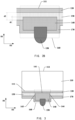
- FIG. 2A is a schematic front view of a solar cell according to another embodiment
- FIG. 2B is an enlarged view of the partial structure in FIG. 2A
- the difference from FIG. 1 is that the barrier layer 140 in FIGs. 2A and 2B goes deep into in the doped polysilicon layer 130 with a predetermined depth d1 in the first direction D1.
- the predetermined depth d1 is equal to or less than the thickness d2 of the doped polysilicon layer 130.
- the present disclosure does not limit the predetermined depth d1, which can be 10 %, 20 %, 30 %, 40 %, 50 %, 60 %, 70%, 80 %, 90% or 100 % of the thickness d2.
- the bottom surface 141 of the barrier layer 140 is in contact with the surface of the tunnel oxide layer 120 away from the substrate 110 in the first direction D1.
- the barrier layer 140 is disposed on the surface of the tunnel oxide layer 120 away from the substrate 110 in the first direction D1.
- FIGs. 4A and 4B are schematic front views of solar cells in two embodiments.
- the barrier layer 140 is disposed on the surface of the tunnel oxide layer 120 away from the substrate 110 in the first direction D1, that is, the bottom surface 141 of the barrier layer 140 is in contact with the tunnel oxide layer 120.
- the barrier layer 140 has a top surface 142 away from the substrate 110 in the first direction D1
- the doped polysilicon layer 130 has a surface 131 away from the substrate 110 in the first direction D1.
- the top surface 142 of the barrier layer 140 is flush with the surface 131 of the doped polysilicon layer 130.
- FIG. 4B the difference between FIG. 4B and FIG.
- top surface 142 of the barrier layer 140 in FIG. 4B is closer to the substrate 110 than the surface 131 of the doped polysilicon layer 130.
- the top surface 142 may also be far away from the substrate 110 than the surface 131 in the first direction D, that is, the barrier layer 140 protrudes from the surface 131 away from the substrate 110.
- the bottom surface 141 of the barrier layer 140 is in contact with the doped polysilicon layer 130.
- the side surfaces of the barrier layer 140 are also in contact with the doped polysilicon layer 130.
- the barrier layer 140 has a first side 143 and a second side 144 opposite to each other in the second direction D2. The first side 143 and the second side 144 are both in contact with the doped polysilicon layer 130. Increasing the contact area between the barrier layer 140 and the doped polysilicon layer 130 is beneficial to reducing resistance.
- the recombination current density of the electrode region in FIGs. 1 to 4B is equal to or less than 100 fA/cm 2 . Reducing the recombination current density helps to improve the efficiency of solar cells.
- a major factor in the recombination current density being equal to or less than 100 fA/cm 2 is that the electrode 150 does not burn through the doped polysilicon layer 130, thereby avoiding contact between the electrode 150 and the substrate 110.
- an ohmic contact is formed between the electrode 150 and the barrier layer 140, and the contact resistance between the two is equal to or less than 1 mohm ⁇ cm 2 .
- the contact resistance can be adjusted by adjusting the doping concentration of the barrier layer 140, for example, increasing the doping concentration can reduce the contact resistance.
- the solar cell in the above embodiments of the present disclosure is provided with a barrier layer in contact with the doped polysilicon layer in the electrode region, which reduces the risk of the electrode burning through the doped polysilicon layer.
- the thickness of the doped polysilicon layer can be further reduced, which reduces the absorption of incident light by the doped polysilicon layer and improves the utilization rate of incident light by the solar cell.
- the present disclosure also includes a method for producing a solar cell, and the method will be described following.
- FIG. 5 is a flow chart of a method for producing a solar cell according to an embodiment. Referring to FIG. 5 , the method according to the embodiment includes the following steps,
- a substrate 110 is provided.
- the substrate 110 has a first surface 111 and a second surface 112 opposite to each other in the first direction D1.
- a tunnel oxide layer 120 is formed on the first surface 111.
- a tunnel oxide layer may be formed on the second surface 112, or a tunnel oxide layer may be formed on both the first surface 111 and the second surface 112.
- a doped polysilicon layer 130 is formed on the surface of the tunnel oxide layer 120 away from the substrate 110 in the first direction D1.
- Methods for forming the tunnel oxide layer 120 and the doped polysilicon layer 130 include chemical vapor deposition (Chemical Vapor Deposition, CVD), physical vapor deposition (Physical Vapor Deposition, PVD), and thermal oxidation.
- CVD chemical Vapor Deposition
- PVD physical vapor deposition
- thermal oxidation thermal oxidation
- the thickness of the doped polysilicon layer 130 is equal to or greater than 3nm and equal to or less than 200nm.
- the thickness of the doped polysilicon layer 130 maybe 3nm, 10nm, 20nm, 30nm, 40nm, 50nm, 60nm, 70nm, 80nm, 90nm, 100nm, 110nm, 120nm, 130nm, 140nm, 150nm, 160nm, 170nm, 180nm, 190nm or 200nm. Since the thickness of the doped polysilicon layer 130 is equal to or greater than 3nm, it can ensure the lateral transmission capability of carriers and ensure that the field passivation of the substrate 110 meets the requirements.
- a barrier layer 140 is formed in the electrode region of the solar cell.
- the barrier layer 140 is in contact with the doped polysilicon layer 130, and the doping type of the barrier layer 140 is the same with the doping type of the doped polysilicon layer 130.
- the doping type of the barrier layer 140 and the doping type of the doped polysilicon layer 130 may both be N-type or P-type.
- the method of forming the barrier layer 140 in FIG. 1 includes the following steps,
- the method of forming the barrier layer 140 in step 12 includes chemical vapor deposition and physical vapor deposition.
- the material of the barrier layer 140 includes one or more of silicon carbide, and zinc oxide.
- FIGs. 2A , 2B , and 6 The intermediate products in the process of producing the solar cells are shown in FIGs. 2A , 2B , and 6 .
- the method of forming the barrier layer 140 in FIGs. 2A and 2B include the following steps:
- the present disclosures do not limit the method of etching the doped polysilicon layer 130.
- it may be physical etching or chemical etching.
- the barrier layer 140 protrudes from the doped polysilicon layer 130 away from the substrate 110.
- the surface of the barrier layer 140 away from the substrate 110 may be flush with the surface of the doped polysilicon layer 130 away from the substrate 110.
- the barrier layer 140 formed in the groove 180 is in contact with the surface of the tunnel oxide layer 120 away from the substrate 110.
- the recombination current density of the electrode region is equal to or less than 100 fA/cm 2 . Reducing the recombination current density helps improve the efficiency of solar cells.
- an electrode is formed, and the electrode is in contact with the barrier layer.
- an electrode 150 is formed in contact with the barrier layer 140.
- An electrical connection is established between the barrier layer 140 and the electrode 150 through contact.
- the electrode 150 in contact with the barrier layer 140 may be formed by a firing method. This disclosure does not limit the depth of the electrode 150 into the barrier layer 140. In some embodiments, the electrode 150 may also penetrate the barrier layer 140, and further go deep into the doped polysilicon layer 130, but not penetrate the polysilicon layer 130.
- a step is further included before step S250: forming a dielectric layer 170 covering a surface of the doped polysilicon layer 130 away from the substrate 110 and a surface of the barrier layer 140 away from the substrate 110.
- the electrode 150 penetrates the dielectric layer 170 and goes deep into the barrier layer 140.
- the producing method in the above embodiments of the present disclosure sets a barrier layer in contact with the doped polysilicon layer in the electrode region, which reduces the risk of the electrode burning through the doped polysilicon layer.
- the thickness of the doped polysilicon layer can be further reduced, which helps to reduce the absorption of incident light by the doped polysilicon layer and improve the utilization rate of incident light by the solar cell.
- numbers are used to describe the quantities of components and properties. It should be understood that such numbers used to describe the embodiments are modified by the modifiers "about”, “approximately” or “substantially” in some examples. Grooming. Unless otherwise stated, “about”, “approximately” or “substantially” means that the stated number is allowed to vary by ⁇ 20%. Accordingly, in some embodiments, the numerical parameters used in the specification and claims are approximations that may vary depending on the desired features of the individual embodiment. In some embodiments, numerical parameters should account for the specified number of significant digits and use general digit preservation methods. Although the numerical fields and parameters used to confirm the breadth of the ranges in some embodiments of the present disclosure are approximations, in specific embodiments, such numerical values are set as accurately as feasible.
Landscapes
- Photovoltaic Devices (AREA)
- Chemical & Material Sciences (AREA)
- Crystallography & Structural Chemistry (AREA)
- Life Sciences & Earth Sciences (AREA)
- Engineering & Computer Science (AREA)
- Sustainable Development (AREA)
- Sustainable Energy (AREA)
Description
- The invention relates to the field of photovoltaic, and specifically relates to a solar cell and a method for producing the solar cell.
- Tunnel Oxide Passivating Contacts solar cell (TOPCon) was proposed in 2014. The solar cell includes a tunnel oxide layer and a doped polysilicon layer. The tunnel oxide layer can selectively transport carriers, and the doped polysilicon layer acts as field passivation. The electrodes of the solar cell penetrate a functional layer (such as an anti-reflection layer) located in the electrode region and contact the doped polysilicon layer.
- The doped polysilicon layer in the solar cell has optical parasitic effects, which results in a decrease in the solar cell's utilization of incident light. Reducing the thickness of the doped polysilicon layer can reduce the absorption of incident light by the doped polysilicon layer, thereby improving the solar cell's utilization of incident light. However, the reduction in the thickness of the doped polysilicon layer increases the risk of the electrode burning through the polysilicon layer, which would result in contact between the electrode and the substrate. Contact between the electrode and the substrate will cause the recombination current density to increase, which will seriously affect the efficiency of the solar cell.
CN 114784148 A describes a preparation method of a solar cell, the solar cell and a photovoltaic module. - Therefore, how to balance the advantage of increasing the utilization rate of incident light with the disadvantage of the increased risk of the electrode burning through the doped polysilicon layer, both of which brought by the reduced thickness of the doped polysilicon layer, is a problem that needs to be solved urgently.
- Some embodiments of the present disclosure are intended to provide a solar cell and a method for producing the solar cell that can reduce the thickness of the doped polysilicon layer while preventing the electrode from burning through the doped polysilicon layer. The invention provides the solar cell according to claim 1 and the method for producing a solar cell according to claim 9.
- Some embodiments provide a solar cell, comprising: a substrate having a first surface and a second surfaces opposite to each other in a first direction, the first direction is a thickness direction of the substrate; a tunnel oxide layer located on the first surface and/or the second surface; a doped polysilicon layer located on a surface of the tunnel oxide layer away from the substrate; a barrier layer located in an electrode region of the solar cell and in contact with the doped polysilicon layer, a doping type of the barrier layer is the same as the doped polysilicon layer; and an electrode located in the electrode region and in contact with the barrier layer; wherein a method of forming the barrier layer includes etching the doped polysilicon layer in the electrode region in the first direction to form a groove with a predetermined depth, and forming the barrier layer in the groove, the predetermined depth is equal to or less than a thickness of the doped polysilicon layer, a material of the barrier layer includes silicon carbide and/or zinc oxide.
- In an embodiment, the barrier layer goes deep into the doped polysilicon layer to the predetermined depth in the first direction.
- In an embodiment, the barrier layer is located on the surface of the tunnel oxide layer away from the substrate.
- In an embodiment, a surface of the barrier layer away from the substrate is flush with a surface of the doped polysilicon layer away from the substrate, or the surface of the barrier layer away from the substrate is closer to the substrate than the surface of the doped polysilicon layer away from the substrate, or the surface of the barrier layer away from the substrate is further away the substrate than the surface of the doped polysilicon layer away from the substrate.
- In an embodiment, a recombination current density of the electrode region is equal to or less than 100 fA/cm2.
- In an embodiment, the solar cell further comprises a dielectric layer, the dielectric layer is located on a surface of the doped polysilicon layer away from the substrate and a surface of the barrier layer away from the substrate.
- In an embodiment, the electrode penetrates the dielectric layer and contacts the barrier layer.
- In an embodiment, the thickness of the doped polysilicon layer is equal to or greater than 3nm, and equal to or less than 200nm.
- Some embodiments further provide a method for producing a solar cell, comprising: providing a substrate having a first surface and a second surfaces opposite to each other in a first direction, the first direction is a thickness direction of the substrate; forming a tunnel oxide layer on the first surface and/or the second surface; forming a doped polysilicon layer on a surface of the tunnel oxide layer away from the substrate; forming a barrier layer in an electrode region of the solar cell, the barrier layer is in contact with the doped polysilicon layer, and a doping type of the barrier layer is the same as the doped polysilicon layer; and forming an electrode in contact with the barrier layer; wherein a method of forming the barrier layer includes etching the doped polysilicon layer in the electrode region in the first direction to form a groove with a predetermined depth, and forming the barrier layer in the groove, the predetermined depth is equal to or less than a thickness of the doped polysilicon layer, and a material of the barrier layer includes silicon carbide and/or zinc oxide.
- In an embodiment, a method of forming the barrier layer includes: cleaning a surface of the doped polysilicon layer; and forming the barrier layer in the electrode region, the barrier layer is in contact with a surface of the doped polysilicon layer away from the substrate.
- In an embodiment, the recombination current density of the electrode region is equal to or less than 100fA/cm2.
- In an embodiment, the thickness of the doped polysilicon layer is equal to or greater than 3nm, and equal to or less than 200nm.
- The solar cell and the producing method thereof of the present disclosure provide the barrier layer in contact with the doped polysilicon layer in the electrode region, which reduces the risk of the electrode burning through the doped polysilicon layer. The thickness of the doped polysilicon can be further reduced, thereby reducing the absorption of incident light by the doped polysilicon layer and improving the utilization rate of incident light by the solar cell.
- In order to make the above purposes, features, and advantages of the present disclosure more obvious and more understandable, the embodiments of the present disclosure are described in detail below with reference to the accompanying drawings.
-
FIG. 1 is a schematic front view of a solar cell according to an embodiment of the present disclosure not forming part of the claimed invention but useful for the understanding thereof; -
FIG. 2A is a schematic front view of a solar cell according to another embodiment of the present disclosure; -
FIG. 2B is an enlarged view of the partial structure inFIG. 2A ; -
FIG. 3 is a schematic front view of a solar cell according to an embodiment of the present disclosure; -
FIGs. 4A and 4B are schematic front views of a solar cell according to two embodiments of the present disclosure; -
FIG. 5 is a flow chart of a method for producing a solar cell according to an embodiment of the present disclosure; -
FIGs. 6 and 7 are intermediate products of a method for producing a solar cell according to different embodiments of the present disclosure. -
Substrate 110,first surface 111,second surface 112,tunnel oxide layer 120, dopedpolysilicon layer 130,initial barrier layer 132,surface 131,barrier layer 140,bottom surface 141,top surface 142,first side surface 143.Second side 144,electrode 150,electrode region 160,dielectric layer 170, andgroove 180. - In order to make the above objects, features, and advantages of the present disclosure more obvious and understandable, the specific implementation modes of the present disclosure are described in detail below with reference to the accompanying drawings.
- Many specific details are set forth in the following description to fully understand the present disclosure, but the present disclosure can also be implemented in other ways different from those described here, so the present disclosure is not limited by the specific embodiments disclosed below.
- As shown in this disclosure and claims, words such as "a", "an", and/or "the" do not specifically refer to the singular and may include the plural unless the context clearly indicates an exception. Generally speaking, the terms "comprising" and "comprising" only imply the inclusion of clearly identified steps and elements, and these steps and elements do not constitute an exclusive list. The method or apparatus may also include other steps or elements.
- In addition, it should be noted that the use of words such as "first" and "second" to define parts is only to facilitate the distinction between corresponding parts. Unless otherwise stated, the above words have no special meaning and therefore cannot be understood. To limit the scope of protection of this disclosure. In addition, although the terms used in this disclosure are selected from well-known and commonly used terms, some terms mentioned in the specification of this disclosure may be selected by the applicant based on his or her judgment, and their detailed meanings are set out herein. stated in the relevant section of the description. Furthermore, the disclosure is required to be understood not merely by the actual terms used, but also by the meaning connoted by each term.
- Flowcharts are used in this disclosure to illustrate operations performed by systems according to embodiments of this disclosure. It should be understood that the preceding or following operations are not necessarily performed in exact order. Instead, the various steps can be processed in reverse order or simultaneously. At the same time, other operations may be added to these processes, or a step or steps may be removed from these processes.
- The solar cell and the method of the present disclosure will be described through specific embodiments.
-
FIG. 1 is a schematic front view of a solar cell according to an embodiment not forming part of the claimed invention but useful for the understanding thereof. Referring toFIG. 1 , a solar cell includes asubstrate 110, atunnel oxide layer 120, a dopedpolysilicon layer 130, abarrier layer 140, and anelectrode 150. Thesubstrate 110 has afirst surface 111 and asecond surface 112 opposite in the first direction D1 (which is also a thickness direction of the substrate 110). Thefirst surface 111 and thesecond surface 112 may be polished or have a pyramid-textured topography. Thetunnel oxide layer 120 is disposed on thefirst surface 111, and the dopedpolysilicon layer 130 is disposed on a surface of thetunnel oxide layer 120 away from thesubstrate 110 in the first direction D1. Thetunnel oxide layer 120 and the dopedpolysilicon layer 130 together form a tunnel oxide layer-doped polysilicon layer passivation structure. It should be noted that in some other embodiments, thetunnel oxide layer 120 can also be formed on thesecond surface 112, or formed on both thefirst surface 111 and thesecond surface 112. - The
substrate 110 may be a silicon substrate, for example, a single crystal silicon substrate or a polycrystalline silicon substrate. Thesubstrate 110 may be doped, such as N-type doping and P-type doping. The material of thetunnel oxide layer 120 may be silicon oxide (SiOx), and the thickness of thetunnel oxide layer 120 may be any value from 1nm to 3nm, for example, 1nm, 1.5nm, 2nm, 2.5nm, or 3nm. Thetunnel oxide layer 120 has a selective collection effect on carriers. The material of the dopedpolysilicon layer 130 can be selected from polysilicon, and the present disclosure does not limit the grain size of the polysilicon. The doping type of the dopedpolysilicon layer 130 may be the same as that of thesubstrate 110, or may be opposite to that of thesubstrate 110. - The solar cell has an electrode region, which is identified in
FIG. 1 using a dashedrectangular frame 160. The electrodes of the solar cell are located in the electrode region. The electrodes are used to collect the electrical energy generated by the solar cell and transmit the electrical energy to the outside. - As shown in
FIG. 1 , thebarrier layer 140 is disposed in the electrode region, and is in contact with the dopedpolysilicon layer 130. The doping type of thebarrier layer 140 is the same as the doping type of the dopedpolysilicon layer 130. For example, the doping type of the dopedpolysilicon layer 130 and the doping type of thebarrier layer 140 are both N-type, and the corresponding doping elements can be selected from phosphorus (P), bismuth (Bi), antimony (Sb), arsenic (As), and other V group elements. The doping type of the dopedpolysilicon layer 130 and the doping type of thebarrier layer 140 can also be P-type, and the corresponding doping elements can be selected from one or more III group elements such as boron (B), aluminum (Al), gallium (Ga), or indium (In). - Continuing with reference to
FIG. 1 , theelectrode 150 is in contact with thebarrier layer 140. It should be understood that the number of the electrode regions and theelectrodes 150 in the solar cell is not limited to the one shown inFIG. 1 . The solar cell includes a certain number of electrode regions andelectrodes 150 spaced apart in the second direction D2, which are not shown inFIG. 1 due to the limited size ofFIG. 1 . - In an embodiment, in
FIG. 1 , the solar cell further includes adielectric layer 170. Thedielectric layer 170 is disposed on the surface of the dopedpolysilicon layer 130 and thebarrier layer 140 away from thesubstrate 110 in the first direction D1. In other words, thedielectric layer 170 covers the exposed surfaces of the dopedpolysilicon layer 130 and thebarrier layer 140. Theelectrode 150 penetrates thedielectric layer 170 and contacts thebarrier layer 140. Thedielectric layer 170 can be a laminated passivation film, which has a passivation effect on the solar cell, and thedielectric layer 170 can also be an anti-reflection film. - In
FIG. 1 , thebarrier layer 140 is disposed on the surface of the dopedpolysilicon layer 130 away from thesubstrate 110 in the first direction D1. Theelectrode 150 is in contact with thebarrier layer 140 through a firing process, thereby forming an electrical connection with thebarrier layer 140 and the doped polysilicon layer 130 (there is an electrical connection between the dopedpolysilicon layer 130 and thebarrier layer 140 due to their contact). InFIG. 1 , theelectrode 150 goes deep into thebarrier layer 140 and does not go deep into the dopedpolysilicon layer 130. In some other embodiments, theelectrode 150 can also penetrate through thebarrier layer 140 and further go deep into the dopedpolysilicon layer 130. - The firing process has an ablation effect on the
barrier layer 140 and the dopedpolysilicon layer 130, which results in the situation in which theelectrode 150 burns through the dopedpolysilicon layer 130 and then contacts thesubstrate 110. The contact between theelectrode 150 and thesubstrate 110 will cause the recombination current density in the electrode region to increase sharply, thereby causing the efficiency of the solar cell to decrease. - Embodiments of the present disclosure form the
barrier layer 140 that is in contact with the dopedpolysilicon layer 130 in the electrode region (where theelectrode 150 is fired). When firing theelectrode 150, the dopedpolysilicon layer 130 will be ablated only after theelectrode 150 burns through thebarrier layer 140. Therefore, thebarrier layer 140 reduces the risk of theelectrode 150 burning through the dopedpolysilicon layer 130. - In one embodiment, the material of the
barrier layer 140 is selected from materials that are more resistant to ablation than the dopedpolysilicon layer 130, such as silicon carbide and/or zinc oxide. Compared with polysilicon with a lower crystallization rate, polysilicon with a higher crystallization rate is more resistant to ablation. In some embodiments, the crystallization rate of the polysilicon in thebarrier layer 140 is equal to or greater than 90%, and the crystallization rate of the dopedpolysilicon layer 130 is 80% to 95%. For example, the crystallization rate of the polysilicon in thebarrier layer 140 maybe 90 %, 95%, 99%, or 100 %, and the crystallization rate of the dopedpolysilicon layer 130 may be 80%, 85%, 90 %, or 95%. In some embodiments, the crystallization rate of the polysilicon in thebarrier layer 140 decreases as the distance from thesubstrate 110 in the first direction D1 decreases. - The material of the
barrier layer 140 may also be a mixture of any two or more of silicon carbide, zinc oxide, and polysilicon. - The technical effect of "the
barrier layer 140 can prevent theelectrode 150 from burning through the dopedpolysilicon layer 130" is briefly described here. InFIG. 1 , thebarrier layer 140 is disposed on the surface of the dopedpolysilicon layer 130 away from thesubstrate 110, which increases the path length for theelectrode 150 to burn through the dopedpolysilicon layer 130, thereby preventing theelectrode 150 from burning through the dopedpolysilicon layer 130. Moreover, when thebarrier layer 140 is selected from an ablation-resistant material, thebarrier layer 140 can also prevent theelectrode 150 from burning through the dopedpolysilicon layer 130 by its own ablation-resistant properties. In short, thebarrier layer 140 can prevent the dopedpolysilicon layer 130 from being burned through by theelectrode 150 by both aspects "increasing the burn-through path" and "its own ablation resistance properties". It should be understood that thebarrier layer 140 can prevent thepolysilicon layer 130 from being burned through by theelectrode 150 through only one, instead of two of the above aspects. - In addition, the doped
polysilicon layer 130 has optical parasitic effect, which reduces the utilization of incident light by the solar cell. Reducing the thickness of dopedpolysilicon layer 130 can reduce its absorption of incident light. However, the technical solution of reducing the thickness of the dopedpolysilicon layer 130 in the conventional technology has a side effect of increasing the risk of theelectrode 150 burning through thetunnel oxide layer 120. The technical solution of setting thebarrier layer 140 in the electrode region in the present disclosure increases the difficulty for theelectrode 150 to burn through the dopedpolysilicon layer 130. Therefore, even if the thickness of the dopedpolysilicon layer 130 is reduced, it can be ensured that theelectrode 150 does not burn through the dopedpolysilicon layer 130, which reduces the absorption of incident light by the dopedpolysilicon layer 130 and improves the solar cell's utilization rate of incident light. In some embodiments, the thickness of the dopedpolysilicon layer 130 is equal to or greater than 3nm and equal to or less than 200nm. For example, the thickness of the dopedpolysilicon layer 130 maybe 3nm, 10nm, 20nm, 30nm, 40nm, 50nm, 60nm, 70nm, 80nm, 90nm, 100nm, 110nm, 120nm, 130nm, 140nm, 150nm, 160nm, 170nm, 180nm, 190nm or 200nm. Since the thickness of the dopedpolysilicon layer 130 is equal to or greater than 3 nm, it can ensure the lateral transport capability of carriers and ensure that the field passivation of thesubstrate 110 meets the requirements. Here,the thickness of the dopedpolysilicon layer 130 refers to the dimension of the dopedpolysilicon layer 130 in the first direction D1. - In
FIG. 1 , thebarrier layer 140 is disposed on the surface of the dopedpolysilicon layer 130 away from thesubstrate 110 in the first direction D1. In the present disclosure, the positional relationship between thebarrier layer 140 and the dopedpolysilicon layer 130 is not limited to that shown inFIG. 1 , which will be described next. -
FIG. 2A is a schematic front view of a solar cell according to another embodiment, andFIG. 2B is an enlarged view of the partial structure inFIG. 2A . Referring toFIGs. 2A and2B , the difference fromFIG. 1 is that thebarrier layer 140 inFIGs. 2A and2B goes deep into in the dopedpolysilicon layer 130 with a predetermined depth d1 in the first direction D1. The predetermined depth d1 is equal to or less than the thickness d2 of the dopedpolysilicon layer 130. The present disclosure does not limit the predetermined depth d1, which can be 10 %, 20 %, 30 %, 40 %, 50 %, 60 %, 70%, 80 %, 90% or 100 % of the thickness d2. It should be understood that when the predetermined depth d1 is equal to the thickness d2 of the dopedpolysilicon layer 130, thebottom surface 141 of thebarrier layer 140 is in contact with the surface of thetunnel oxide layer 120 away from thesubstrate 110 in the first direction D1. In other words, as shown inFIG. 3 , thebarrier layer 140 is disposed on the surface of thetunnel oxide layer 120 away from thesubstrate 110 in the first direction D1. -
FIGs. 4A and 4B are schematic front views of solar cells in two embodiments. Referring toFIG. 4A , thebarrier layer 140 is disposed on the surface of thetunnel oxide layer 120 away from thesubstrate 110 in the first direction D1, that is, thebottom surface 141 of thebarrier layer 140 is in contact with thetunnel oxide layer 120. Thebarrier layer 140 has atop surface 142 away from thesubstrate 110 in the first direction D1, and the dopedpolysilicon layer 130 has asurface 131 away from thesubstrate 110 in the first direction D1. InFIG. 4A , thetop surface 142 of thebarrier layer 140 is flush with thesurface 131 of the dopedpolysilicon layer 130. Referring toFIG. 4B , the difference betweenFIG. 4B and FIG. 4A is that thetop surface 142 of thebarrier layer 140 inFIG. 4B is closer to thesubstrate 110 than thesurface 131 of the dopedpolysilicon layer 130. In some other embodiments, thetop surface 142 may also be far away from thesubstrate 110 than thesurface 131 in the first direction D, that is, thebarrier layer 140 protrudes from thesurface 131 away from thesubstrate 110. - In
FIG. 1 , thebottom surface 141 of thebarrier layer 140 is in contact with the dopedpolysilicon layer 130. InFIGs. 2A to 4B , in addition to thebottom surface 141, the side surfaces of thebarrier layer 140 are also in contact with the dopedpolysilicon layer 130. TakingFIG. 3 as an example, thebarrier layer 140 has afirst side 143 and asecond side 144 opposite to each other in the second direction D2. Thefirst side 143 and thesecond side 144 are both in contact with the dopedpolysilicon layer 130. Increasing the contact area between thebarrier layer 140 and the dopedpolysilicon layer 130 is beneficial to reducing resistance. - In one embodiment, the recombination current density of the electrode region in
FIGs. 1 to 4B is equal to or less than 100 fA/cm2. Reducing the recombination current density helps to improve the efficiency of solar cells. A major factor in the recombination current density being equal to or less than 100 fA/cm2 is that theelectrode 150 does not burn through the dopedpolysilicon layer 130, thereby avoiding contact between theelectrode 150 and thesubstrate 110. In some other embodiments, an ohmic contact is formed between theelectrode 150 and thebarrier layer 140, and the contact resistance between the two is equal to or less than 1 mohm·cm2. The contact resistance can be adjusted by adjusting the doping concentration of thebarrier layer 140, for example, increasing the doping concentration can reduce the contact resistance. - The solar cell in the above embodiments of the present disclosure is provided with a barrier layer in contact with the doped polysilicon layer in the electrode region, which reduces the risk of the electrode burning through the doped polysilicon layer. The thickness of the doped polysilicon layer can be further reduced, which reduces the absorption of incident light by the doped polysilicon layer and improves the utilization rate of incident light by the solar cell.
- The present disclosure also includes a method for producing a solar cell, and the method will be described following.
-
FIG. 5 is a flow chart of a method for producing a solar cell according to an embodiment. Referring toFIG. 5 , the method according to the embodiment includes the following steps, - Step S210: providing a substrate having a first surface and a second surface opposite to each other in a first direction;
- Step S220: forming a tunnel oxide layer on the first surface and/or the second surface;
- Step S230: forming a doped polysilicon layer on the surface of the tunnel oxide layer away from the substrate;
- Step S240: forming a barrier layer in the electrode region of the solar cell, wherein the barrier layer is in contact with the doped polysilicon layer, and the doping type of the barrier layer is the same as the doped polysilicon layer;
- Step S250: forming an electrode, the electrode being in contact with the barrier layer.
- Next, steps S210 to S250 will be described in detail.
- Referring to
FIG. 1 , in step S210, asubstrate 110 is provided. Thesubstrate 110 has afirst surface 111 and asecond surface 112 opposite to each other in the first direction D1. In step S220, atunnel oxide layer 120 is formed on thefirst surface 111. In some other embodiments, a tunnel oxide layer may be formed on thesecond surface 112, or a tunnel oxide layer may be formed on both thefirst surface 111 and thesecond surface 112. In step S230, a dopedpolysilicon layer 130 is formed on the surface of thetunnel oxide layer 120 away from thesubstrate 110 in the first direction D1. Methods for forming thetunnel oxide layer 120 and the dopedpolysilicon layer 130 include chemical vapor deposition (Chemical Vapor Deposition, CVD), physical vapor deposition (Physical Vapor Deposition, PVD), and thermal oxidation. For other descriptions about thesubstrate 110, thetunnel oxide layer 120, and the dopedpolysilicon layer 130, please refer to the relevant parts above and would not be elaborated here. - In one embodiment, the thickness of the doped
polysilicon layer 130 is equal to or greater than 3nm and equal to or less than 200nm. For example, the thickness of the dopedpolysilicon layer 130 maybe 3nm, 10nm, 20nm, 30nm, 40nm, 50nm, 60nm, 70nm, 80nm, 90nm, 100nm, 110nm, 120nm, 130nm, 140nm, 150nm, 160nm, 170nm, 180nm, 190nm or 200nm. Since the thickness of the dopedpolysilicon layer 130 is equal to or greater than 3nm, it can ensure the lateral transmission capability of carriers and ensure that the field passivation of thesubstrate 110 meets the requirements. - Continuing to refer to
FIG. 1 , in step S240, abarrier layer 140 is formed in the electrode region of the solar cell. Thebarrier layer 140 is in contact with the dopedpolysilicon layer 130, and the doping type of thebarrier layer 140 is the same with the doping type of the dopedpolysilicon layer 130. The doping type of thebarrier layer 140 and the doping type of the dopedpolysilicon layer 130 may both be N-type or P-type. - In one embodiment, the method of forming the
barrier layer 140 inFIG. 1 includes the following steps, - Step 11: cleaning the surface of the doped
polysilicon layer 130. The surface includes a surface of the dopedpolysilicon layer 130 away from thesubstrate 110 in the first direction D1. The contaminants on the surface of the dopedpolysilicon layer 130 can be removed through the cleaning process. - Step 12: forming a
barrier layer 140 in the electrode region, thebarrier layer 140 is in contact with the surface of the dopedpolysilicon layer 130 away from thesubstrate 110 in the first direction D1. - The method of forming the
barrier layer 140 in step 12 includes chemical vapor deposition and physical vapor deposition. The material of thebarrier layer 140 includes one or more of silicon carbide, and zinc oxide. - The intermediate products in the process of producing the solar cells are shown in
FIGs. 2A ,2B , and6 . In one embodiment, the method of forming thebarrier layer 140 inFIGs. 2A and2B include the following steps: - Step 21: etching the doped
polysilicon layer 130 in the electrode region in the first direction D1 to form agroove 180 with a predetermined depth d3. - Step 22: forming the
barrier layer 140 in thegroove 180, the predetermined depth d3 is equal to or less than the thickness d4 of the dopedpolysilicon layer 130. - The present disclosures do not limit the method of etching the doped
polysilicon layer 130. For example, it may be physical etching or chemical etching. As shown inFIGs. 2A and2B , thebarrier layer 140 protrudes from the dopedpolysilicon layer 130 away from thesubstrate 110. In some other embodiments, the surface of thebarrier layer 140 away from thesubstrate 110 may be flush with the surface of the dopedpolysilicon layer 130 away from thesubstrate 110. - As shown in
FIG. 3 andFIG. 6 , when the predetermined depth d3 is equal to the thickness d4 of the dopedpolysilicon layer 130, thebarrier layer 140 formed in thegroove 180 is in contact with the surface of thetunnel oxide layer 120 away from thesubstrate 110. - In one embodiment, the recombination current density of the electrode region is equal to or less than 100 fA/cm2. Reducing the recombination current density helps improve the efficiency of solar cells.
- Returning to
FIG. 5 , in step S250, an electrode is formed, and the electrode is in contact with the barrier layer. TakingFIG. 1 as an example for explanation, anelectrode 150 is formed in contact with thebarrier layer 140. An electrical connection is established between thebarrier layer 140 and theelectrode 150 through contact. Theelectrode 150 in contact with thebarrier layer 140 may be formed by a firing method. This disclosure does not limit the depth of theelectrode 150 into thebarrier layer 140. In some embodiments, theelectrode 150 may also penetrate thebarrier layer 140, and further go deep into the dopedpolysilicon layer 130, but not penetrate thepolysilicon layer 130. - Referring to
FIG. 1 , in some embodiments, a step is further included before step S250: forming adielectric layer 170 covering a surface of the dopedpolysilicon layer 130 away from thesubstrate 110 and a surface of thebarrier layer 140 away from thesubstrate 110. In step S250, theelectrode 150 penetrates thedielectric layer 170 and goes deep into thebarrier layer 140. - The producing method in the above embodiments of the present disclosure sets a barrier layer in contact with the doped polysilicon layer in the electrode region, which reduces the risk of the electrode burning through the doped polysilicon layer. The thickness of the doped polysilicon layer can be further reduced, which helps to reduce the absorption of incident light by the doped polysilicon layer and improve the utilization rate of incident light by the solar cell.
- The basic concepts have been described above. Obviously, for those skilled in the art, the above disclosure disclosures are only examples and do not constitute limitations to the present disclosure. Although not explicitly stated herein, those skilled in the art may make various modifications, improvements, and corrections to this disclosure.
- At the same time, this disclosure uses specific words to describe the embodiments of the disclosure. For example, "one embodiment", "an embodiment", and/or "some embodiments" means a certain feature, structure or characteristic related to at least one embodiment of the present disclosure. Therefore, it should be emphasized and noted that "one embodiment" or "an embodiment" or "an alternative embodiment" mentioned twice or more at different places in this specification does not necessarily refer to the same embodiment.. In addition, certain features, structures or characteristics in one or more embodiments of the present disclosure may be appropriately combined.
- In some embodiments, numbers are used to describe the quantities of components and properties. It should be understood that such numbers used to describe the embodiments are modified by the modifiers "about", "approximately" or "substantially" in some examples. Grooming. Unless otherwise stated, "about", "approximately" or "substantially" means that the stated number is allowed to vary by ± 20%. Accordingly, in some embodiments, the numerical parameters used in the specification and claims are approximations that may vary depending on the desired features of the individual embodiment. In some embodiments, numerical parameters should account for the specified number of significant digits and use general digit preservation methods. Although the numerical fields and parameters used to confirm the breadth of the ranges in some embodiments of the present disclosure are approximations, in specific embodiments, such numerical values are set as accurately as feasible.
Claims (12)
- A solar cell, comprising:a substrate(110) having a first surface(111) and a second surface(112) opposite to each other in a first direction(D1), wherein the first direction(D1) is a thickness direction of the substrate(110);a tunnel oxide layer(120) located on the first surface(111) and/or the second surface(112);a doped polysilicon layer(130) located on a surface of the tunnel oxide layer(120) away from the substrate(110);a barrier layer(140) located in an electrode region(160) of the solar cell and in contact with the doped polysilicon layer(130), wherein a doping type of the barrier layer(140) is the same as the doped polysilicon layer(130);an electrode(150) located in the electrode region(160) and in contact with the barrier layer(140);characterized in that a method of forming the barrier layer(140) includes etching the doped polysilicon layer(130) in the electrode region(150) in the first direction to form a groove(180) with a predetermined depth(d3), and forming the barrier layer(140) in the groove(180), wherein the predetermined depth(d3) is equal to or less than a thickness of the doped polysilicon layer(130), a material of the barrier layer(140) includes silicon carbide and/or zinc oxide.
- The solar cell of claim 1, wherein the barrier layer goes deep into the doped polysilicon layer to the predetermined depth in the first direction.
- The solar cell of claim 1, wherein the barrier layer is located on the surface of the tunnel oxide layer away from the substrate.
- The solar cell of claim 3, wherein a surface of the barrier layer away from the substrate is flush with a surface of the doped polysilicon layer away from the substrate, or the surface of the barrier layer away from the substrate is closer to the substrate than the surface of the doped polysilicon layer away from the substrate, or the surface of the barrier layer away from the substrate is further away from the substrate than the surface of the doped polysilicon layer away from the substrate.
- The solar cell of claim 1, wherein a recombination current density of the electrode region is equal to or less than 100fA/cm2.
- The solar cell of claim 1, further comprising a dielectric layer(170), wherein the dielectric layer is located on a surface of the doped polysilicon layer away from the substrate and a surface of the barrier layer away from the substrate.
- The solar cell of claim 6, wherein the electrode penetrates the dielectric layer and contacts the barrier layer.
- The solar cell according to claim 1, wherein the thickness of the doped polysilicon layer is equal to or greater than 3nm, and equal to or less than 200nm.
- A method for producing a solar cell, comprising:providing a substrate having a first surface and a second surface opposite to each other in a first direction, wherein the first direction is a thickness direction of the substrate;forming a tunnel oxide layer on the first surface and/or the second surface;forming a doped polysilicon layer on a surface of the tunnel oxide layer away from the substrate;forming a barrier layer in an electrode region of the solar cell, wherein the barrier layer is in contact with the doped polysilicon layer, and a doping type of the barrier layer is the same as the doped polysilicon layer; andforming an electrode in contact with the barrier layer;characterized in that a method of forming the barrier layer includes etching the doped polysilicon layer in the electrode region in the first direction to form a groove with a predetermined depth, and forming the barrier layer in the groove, wherein the predetermined depth is equal to or less than a thickness of the doped polysilicon layer, and a material of the barrier layer includes silicon carbide and/or zinc oxide.
- The method of claim 9, wherein a method of forming the barrier layer includes:cleaning a surface of the doped polysilicon layer;forming the barrier layer in the electrode region, wherein the barrier layer is in contact with a surface of the doped polysilicon layer away from the substrate.
- The method of claim 9, wherein the recombination current density of the electrode region is equal to or less than 100fA/cm2.
- The method of claim 9, wherein the thickness of the doped polysilicon layer is equal to or greater than 3nm, and equal to or less than 200nm.
Priority Applications (1)
| Application Number | Priority Date | Filing Date | Title |
|---|---|---|---|
| EP25174460.3A EP4572569A3 (en) | 2023-06-21 | 2023-11-08 | Solar cell and method for producing the solar cell |
Applications Claiming Priority (1)
| Application Number | Priority Date | Filing Date | Title |
|---|---|---|---|
| CN202310741576.2A CN116487452B (en) | 2023-06-21 | 2023-06-21 | Solar cell and method for producing solar cell |
Related Child Applications (1)
| Application Number | Title | Priority Date | Filing Date |
|---|---|---|---|
| EP25174460.3A Division EP4572569A3 (en) | 2023-06-21 | 2023-11-08 | Solar cell and method for producing the solar cell |
Publications (3)
| Publication Number | Publication Date |
|---|---|
| EP4481834A1 EP4481834A1 (en) | 2024-12-25 |
| EP4481834C0 EP4481834C0 (en) | 2025-06-04 |
| EP4481834B1 true EP4481834B1 (en) | 2025-06-04 |
Family
ID=87212289
Family Applications (2)
| Application Number | Title | Priority Date | Filing Date |
|---|---|---|---|
| EP25174460.3A Pending EP4572569A3 (en) | 2023-06-21 | 2023-11-08 | Solar cell and method for producing the solar cell |
| EP23208472.3A Active EP4481834B1 (en) | 2023-06-21 | 2023-11-08 | Solar cell and method for producing the solar cell |
Family Applications Before (1)
| Application Number | Title | Priority Date | Filing Date |
|---|---|---|---|
| EP25174460.3A Pending EP4572569A3 (en) | 2023-06-21 | 2023-11-08 | Solar cell and method for producing the solar cell |
Country Status (5)
| Country | Link |
|---|---|
| US (1) | US20240429327A1 (en) |
| EP (2) | EP4572569A3 (en) |
| JP (2) | JP7688093B2 (en) |
| CN (1) | CN116487452B (en) |
| AU (1) | AU2023263466B2 (en) |
Families Citing this family (4)
| Publication number | Priority date | Publication date | Assignee | Title |
|---|---|---|---|---|
| CN116487452B (en) * | 2023-06-21 | 2023-10-27 | 天合光能股份有限公司 | Solar cell and method for producing solar cell |
| CN117438481B (en) * | 2023-12-20 | 2024-04-09 | 淮安捷泰新能源科技有限公司 | Photovoltaic module and preparation method thereof, and preparation method of N-TOPCO battery piece |
| CN117936616B (en) * | 2024-03-21 | 2024-06-21 | 天合光能股份有限公司 | Solar cell and manufacturing method thereof, photovoltaic module and photovoltaic system |
| EP4629786A1 (en) * | 2024-04-01 | 2025-10-08 | Jinko Solar (Haining) Co., Ltd. | Solar cell, photovoltaic module and method for forming solar cell |
Family Cites Families (17)
| Publication number | Priority date | Publication date | Assignee | Title |
|---|---|---|---|---|
| US20110088760A1 (en) * | 2009-10-20 | 2011-04-21 | Applied Materials, Inc. | Methods of forming an amorphous silicon layer for thin film solar cell application |
| KR102498523B1 (en) * | 2019-10-16 | 2023-02-10 | 상라오 징코 솔라 테크놀러지 디벨롭먼트 컴퍼니, 리미티드 | Solar cell and method for manufacturing the same |
| CN111009583B (en) * | 2019-12-10 | 2022-03-22 | 江苏微导纳米科技股份有限公司 | Topcon structure battery and preparation method thereof |
| CN113871494B (en) * | 2020-06-30 | 2024-03-15 | 泰州隆基乐叶光伏科技有限公司 | Solar cell and manufacturing method thereof |
| CN112466962B (en) | 2020-11-19 | 2021-11-23 | 晶科绿能(上海)管理有限公司 | Solar cell |
| CN112736159A (en) * | 2020-12-31 | 2021-04-30 | 三江学院 | Preparation method of selective polycrystalline silicon thickness and doping concentration battery structure |
| CN214753793U (en) * | 2021-06-04 | 2021-11-16 | 浙江爱旭太阳能科技有限公司 | P-type back contact type crystalline silicon solar cell and solar cell module |
| CN114649427B (en) * | 2021-09-14 | 2023-09-12 | 浙江晶科能源有限公司 | Solar cell and photovoltaic module |
| CN113838941B (en) | 2021-11-23 | 2022-02-11 | 浙江爱旭太阳能科技有限公司 | A selective passivation contact structure for solar cells and bifacial solar cells |
| CN114335250B (en) * | 2021-12-30 | 2023-03-24 | 泰州中来光电科技有限公司 | Preparation method and application method of passivation contact structure |
| CN114709294B (en) * | 2022-05-31 | 2022-11-29 | 浙江晶科能源有限公司 | Solar cell, preparation method thereof and photovoltaic module |
| CN114784148B (en) * | 2022-06-15 | 2022-09-23 | 浙江晶科能源有限公司 | Preparation method of solar cell, solar cell and photovoltaic module |
| CN115148857A (en) * | 2022-07-14 | 2022-10-04 | 上饶捷泰新能源科技有限公司 | TOPCon battery and manufacturing method thereof |
| CN115985975B (en) * | 2023-02-02 | 2026-04-28 | 浙江晶科能源有限公司 | Solar cells and photovoltaic modules |
| CN116581174A (en) * | 2023-02-22 | 2023-08-11 | 浙江晶科能源有限公司 | Solar cell and its preparation method, photovoltaic module |
| CN116487452B (en) * | 2023-06-21 | 2023-10-27 | 天合光能股份有限公司 | Solar cell and method for producing solar cell |
| CN116632077A (en) | 2023-07-12 | 2023-08-22 | 东方日升新能源股份有限公司 | N-type TOPCON photovoltaic cell and preparation method thereof |
-
2023
- 2023-06-21 CN CN202310741576.2A patent/CN116487452B/en active Active
- 2023-11-08 AU AU2023263466A patent/AU2023263466B2/en active Active
- 2023-11-08 JP JP2023190883A patent/JP7688093B2/en active Active
- 2023-11-08 EP EP25174460.3A patent/EP4572569A3/en active Pending
- 2023-11-08 EP EP23208472.3A patent/EP4481834B1/en active Active
- 2023-11-30 US US18/524,791 patent/US20240429327A1/en active Pending
-
2025
- 2025-05-21 JP JP2025085025A patent/JP2025118985A/en active Pending
Also Published As
| Publication number | Publication date |
|---|---|
| CN116487452A (en) | 2023-07-25 |
| EP4481834A1 (en) | 2024-12-25 |
| AU2023263466B2 (en) | 2025-07-10 |
| JP2025118985A (en) | 2025-08-13 |
| JP2025003266A (en) | 2025-01-09 |
| US20240429327A1 (en) | 2024-12-26 |
| AU2023263466A1 (en) | 2025-01-16 |
| EP4481834C0 (en) | 2025-06-04 |
| EP4572569A3 (en) | 2026-02-11 |
| JP7688093B2 (en) | 2025-06-03 |
| CN116487452B (en) | 2023-10-27 |
| EP4572569A2 (en) | 2025-06-18 |
Similar Documents
| Publication | Publication Date | Title |
|---|---|---|
| EP4572569A2 (en) | Solar cell and method for producing the solar cell | |
| EP4123723B1 (en) | Passivated contact structure and solar cell comprising the same, cell assembly, and photovoltaic system | |
| AU2023282191B2 (en) | Doped region structure and solar cell comprising the same, cell assembly, and photovoltaic system | |
| US20250261473A1 (en) | Passivated contact structure and solar cell comprising the same, cell assembly, and photovoltaic system | |
| CN112289873A (en) | Solar cell | |
| CN117712212B (en) | Solar cell and method for manufacturing solar cell | |
| KR20130052627A (en) | Back junction solar cell with selective front surface field | |
| US12598818B2 (en) | Doped region structure and solar cell comprising the same, cell assembly, and photovoltaic system | |
| US11837671B2 (en) | Doped region structure and solar cell comprising the same, cell assembly, and photovoltaic system | |
| CN119866068B (en) | Back contact battery with specific passivation structure and manufacturing method and application thereof | |
| JP2024022416A (en) | Solar cells and solar cell manufacturing methods, photovoltaic modules | |
| US20250151454A1 (en) | Doped region structure and solar cell comprising the same, cell assembly, and photovoltaic system | |
| KR102611046B1 (en) | Solar cell | |
| CN118738153A (en) | Solar cells and photovoltaic modules | |
| CN224054707U (en) | Solar cell | |
| TWI667797B (en) | Solar cell | |
| TW202539458A (en) | Back-contact solar cell and method for producing a back-contact solar cell | |
| CN120769567A (en) | A low-cost, high-performance solar cell and its manufacturing process | |
| CN122054748A (en) | Back contact battery, battery assembly and photovoltaic system | |
| CN119451311A (en) | Solar cell and preparation method thereof, photovoltaic module |
Legal Events
| Date | Code | Title | Description |
|---|---|---|---|
| PUAI | Public reference made under article 153(3) epc to a published international application that has entered the european phase |
Free format text: ORIGINAL CODE: 0009012 |
|
| STAA | Information on the status of an ep patent application or granted ep patent |
Free format text: STATUS: THE APPLICATION HAS BEEN PUBLISHED |
|
| AK | Designated contracting states |
Kind code of ref document: A1 Designated state(s): AL AT BE BG CH CY CZ DE DK EE ES FI FR GB GR HR HU IE IS IT LI LT LU LV MC ME MK MT NL NO PL PT RO RS SE SI SK SM TR |
|
| STAA | Information on the status of an ep patent application or granted ep patent |
Free format text: STATUS: REQUEST FOR EXAMINATION WAS MADE |
|
| 17P | Request for examination filed |
Effective date: 20250114 |
|
| REG | Reference to a national code |
Ref country code: DE Ref legal event code: R079 Free format text: PREVIOUS MAIN CLASS: H01L0031074700 Ipc: H10F0010166000 Ref country code: DE Ref legal event code: R079 Ref document number: 602023003841 Country of ref document: DE Free format text: PREVIOUS MAIN CLASS: H01L0031074700 Ipc: H10F0010166000 |
|
| GRAP | Despatch of communication of intention to grant a patent |
Free format text: ORIGINAL CODE: EPIDOSNIGR1 |
|
| STAA | Information on the status of an ep patent application or granted ep patent |
Free format text: STATUS: GRANT OF PATENT IS INTENDED |
|
| RIC1 | Information provided on ipc code assigned before grant |
Ipc: H10F 77/20 20250101ALI20250319BHEP Ipc: H10F 10/166 20250101AFI20250319BHEP |
|
| GRAS | Grant fee paid |
Free format text: ORIGINAL CODE: EPIDOSNIGR3 |
|
| INTG | Intention to grant announced |
Effective date: 20250326 |
|
| GRAA | (expected) grant |
Free format text: ORIGINAL CODE: 0009210 |
|
| STAA | Information on the status of an ep patent application or granted ep patent |
Free format text: STATUS: THE PATENT HAS BEEN GRANTED |
|
| AK | Designated contracting states |
Kind code of ref document: B1 Designated state(s): AL AT BE BG CH CY CZ DE DK EE ES FI FR GB GR HR HU IE IS IT LI LT LU LV MC ME MK MT NL NO PL PT RO RS SE SI SK SM TR |
|
| REG | Reference to a national code |
Ref country code: GB Ref legal event code: FG4D |
|
| REG | Reference to a national code |
Ref country code: CH Ref legal event code: EP |
|
| REG | Reference to a national code |
Ref country code: DE Ref legal event code: R096 Ref document number: 602023003841 Country of ref document: DE |
|
| REG | Reference to a national code |
Ref country code: IE Ref legal event code: FG4D |
|
| U01 | Request for unitary effect filed |
Effective date: 20250624 |
|
| U07 | Unitary effect registered |
Designated state(s): AT BE BG DE DK EE FI FR IT LT LU LV MT NL PT RO SE SI Effective date: 20250701 |
|
| PG25 | Lapsed in a contracting state [announced via postgrant information from national office to epo] |
Ref country code: ES Free format text: LAPSE BECAUSE OF FAILURE TO SUBMIT A TRANSLATION OF THE DESCRIPTION OR TO PAY THE FEE WITHIN THE PRESCRIBED TIME-LIMIT Effective date: 20250604 |
|
| PG25 | Lapsed in a contracting state [announced via postgrant information from national office to epo] |
Ref country code: NO Free format text: LAPSE BECAUSE OF FAILURE TO SUBMIT A TRANSLATION OF THE DESCRIPTION OR TO PAY THE FEE WITHIN THE PRESCRIBED TIME-LIMIT Effective date: 20250904 Ref country code: GR Free format text: LAPSE BECAUSE OF FAILURE TO SUBMIT A TRANSLATION OF THE DESCRIPTION OR TO PAY THE FEE WITHIN THE PRESCRIBED TIME-LIMIT Effective date: 20250905 |
|
| PG25 | Lapsed in a contracting state [announced via postgrant information from national office to epo] |
Ref country code: PL Free format text: LAPSE BECAUSE OF FAILURE TO SUBMIT A TRANSLATION OF THE DESCRIPTION OR TO PAY THE FEE WITHIN THE PRESCRIBED TIME-LIMIT Effective date: 20250604 |
|
| PG25 | Lapsed in a contracting state [announced via postgrant information from national office to epo] |
Ref country code: HR Free format text: LAPSE BECAUSE OF FAILURE TO SUBMIT A TRANSLATION OF THE DESCRIPTION OR TO PAY THE FEE WITHIN THE PRESCRIBED TIME-LIMIT Effective date: 20250604 |
|
| PG25 | Lapsed in a contracting state [announced via postgrant information from national office to epo] |
Ref country code: RS Free format text: LAPSE BECAUSE OF FAILURE TO SUBMIT A TRANSLATION OF THE DESCRIPTION OR TO PAY THE FEE WITHIN THE PRESCRIBED TIME-LIMIT Effective date: 20250904 |
|
| U20 | Renewal fee for the european patent with unitary effect paid |
Year of fee payment: 3 Effective date: 20251110 |
|
| PG25 | Lapsed in a contracting state [announced via postgrant information from national office to epo] |
Ref country code: IS Free format text: LAPSE BECAUSE OF FAILURE TO SUBMIT A TRANSLATION OF THE DESCRIPTION OR TO PAY THE FEE WITHIN THE PRESCRIBED TIME-LIMIT Effective date: 20251004 |
|
| PG25 | Lapsed in a contracting state [announced via postgrant information from national office to epo] |
Ref country code: SM Free format text: LAPSE BECAUSE OF FAILURE TO SUBMIT A TRANSLATION OF THE DESCRIPTION OR TO PAY THE FEE WITHIN THE PRESCRIBED TIME-LIMIT Effective date: 20250604 |
|
| PG25 | Lapsed in a contracting state [announced via postgrant information from national office to epo] |
Ref country code: CZ Free format text: LAPSE BECAUSE OF FAILURE TO SUBMIT A TRANSLATION OF THE DESCRIPTION OR TO PAY THE FEE WITHIN THE PRESCRIBED TIME-LIMIT Effective date: 20250604 |
|
| PG25 | Lapsed in a contracting state [announced via postgrant information from national office to epo] |
Ref country code: SK Free format text: LAPSE BECAUSE OF FAILURE TO SUBMIT A TRANSLATION OF THE DESCRIPTION OR TO PAY THE FEE WITHIN THE PRESCRIBED TIME-LIMIT Effective date: 20250604 |
|
| PLBE | No opposition filed within time limit |
Free format text: ORIGINAL CODE: 0009261 |
|
| STAA | Information on the status of an ep patent application or granted ep patent |
Free format text: STATUS: NO OPPOSITION FILED WITHIN TIME LIMIT |
|
| REG | Reference to a national code |
Ref country code: CH Ref legal event code: L10 Free format text: ST27 STATUS EVENT CODE: U-0-0-L10-L00 (AS PROVIDED BY THE NATIONAL OFFICE) Effective date: 20260416 |
|
| 26N | No opposition filed |
Effective date: 20260305 |