EP4481819A1 - Semiconductor package, semiconductor package intermediate body, rewiring layer chip, rewiring layer chip intermediate body, semiconductor package manufacturing method, and semiconductor package intermediate body manufacturing method - Google Patents
Semiconductor package, semiconductor package intermediate body, rewiring layer chip, rewiring layer chip intermediate body, semiconductor package manufacturing method, and semiconductor package intermediate body manufacturing method Download PDFInfo
- Publication number
- EP4481819A1 EP4481819A1 EP23756417.4A EP23756417A EP4481819A1 EP 4481819 A1 EP4481819 A1 EP 4481819A1 EP 23756417 A EP23756417 A EP 23756417A EP 4481819 A1 EP4481819 A1 EP 4481819A1
- Authority
- EP
- European Patent Office
- Prior art keywords
- redistribution
- layer
- interposer
- chip
- redistribution layer
- Prior art date
- Legal status (The legal status is an assumption and is not a legal conclusion. Google has not performed a legal analysis and makes no representation as to the accuracy of the status listed.)
- Pending
Links
Images












Classifications
-
- H—ELECTRICITY
- H10—SEMICONDUCTOR DEVICES; ELECTRIC SOLID-STATE DEVICES NOT OTHERWISE PROVIDED FOR
- H10W—GENERIC PACKAGES, INTERCONNECTIONS, CONNECTORS OR OTHER CONSTRUCTIONAL DETAILS OF DEVICES COVERED BY CLASS H10
- H10W90/00—Package configurations
-
- H—ELECTRICITY
- H10—SEMICONDUCTOR DEVICES; ELECTRIC SOLID-STATE DEVICES NOT OTHERWISE PROVIDED FOR
- H10B—ELECTRONIC MEMORY DEVICES
- H10B80/00—Assemblies of multiple devices comprising at least one memory device covered by this subclass
-
- H—ELECTRICITY
- H10—SEMICONDUCTOR DEVICES; ELECTRIC SOLID-STATE DEVICES NOT OTHERWISE PROVIDED FOR
- H10W—GENERIC PACKAGES, INTERCONNECTIONS, CONNECTORS OR OTHER CONSTRUCTIONAL DETAILS OF DEVICES COVERED BY CLASS H10
- H10W70/00—Package substrates; Interposers; Redistribution layers [RDL]
- H10W70/60—Insulating or insulated package substrates; Interposers; Redistribution layers
- H10W70/611—Insulating or insulated package substrates; Interposers; Redistribution layers for connecting multiple chips together
- H10W70/616—Insulating or insulated package substrates; Interposers; Redistribution layers for connecting multiple chips together package substrates, interposers or redistribution layers combined with bridge chips
- H10W70/618—Insulating or insulated package substrates; Interposers; Redistribution layers for connecting multiple chips together package substrates, interposers or redistribution layers combined with bridge chips the bridge chips being embedded in the package substrates, interposers or redistribution layers
-
- H—ELECTRICITY
- H10—SEMICONDUCTOR DEVICES; ELECTRIC SOLID-STATE DEVICES NOT OTHERWISE PROVIDED FOR
- H10W—GENERIC PACKAGES, INTERCONNECTIONS, CONNECTORS OR OTHER CONSTRUCTIONAL DETAILS OF DEVICES COVERED BY CLASS H10
- H10W20/00—Interconnections in chips, wafers or substrates
- H10W20/20—Interconnections within wafers or substrates, e.g. through-silicon vias [TSV]
-
- H—ELECTRICITY
- H10—SEMICONDUCTOR DEVICES; ELECTRIC SOLID-STATE DEVICES NOT OTHERWISE PROVIDED FOR
- H10W—GENERIC PACKAGES, INTERCONNECTIONS, CONNECTORS OR OTHER CONSTRUCTIONAL DETAILS OF DEVICES COVERED BY CLASS H10
- H10W70/00—Package substrates; Interposers; Redistribution layers [RDL]
- H10W70/60—Insulating or insulated package substrates; Interposers; Redistribution layers
- H10W70/611—Insulating or insulated package substrates; Interposers; Redistribution layers for connecting multiple chips together
-
- H—ELECTRICITY
- H10—SEMICONDUCTOR DEVICES; ELECTRIC SOLID-STATE DEVICES NOT OTHERWISE PROVIDED FOR
- H10W—GENERIC PACKAGES, INTERCONNECTIONS, CONNECTORS OR OTHER CONSTRUCTIONAL DETAILS OF DEVICES COVERED BY CLASS H10
- H10W70/00—Package substrates; Interposers; Redistribution layers [RDL]
- H10W70/60—Insulating or insulated package substrates; Interposers; Redistribution layers
- H10W70/62—Insulating or insulated package substrates; Interposers; Redistribution layers characterised by their interconnections
- H10W70/63—Vias, e.g. via plugs
- H10W70/635—Through-vias
-
- H—ELECTRICITY
- H10—SEMICONDUCTOR DEVICES; ELECTRIC SOLID-STATE DEVICES NOT OTHERWISE PROVIDED FOR
- H10W—GENERIC PACKAGES, INTERCONNECTIONS, CONNECTORS OR OTHER CONSTRUCTIONAL DETAILS OF DEVICES COVERED BY CLASS H10
- H10W70/00—Package substrates; Interposers; Redistribution layers [RDL]
- H10W70/60—Insulating or insulated package substrates; Interposers; Redistribution layers
- H10W70/62—Insulating or insulated package substrates; Interposers; Redistribution layers characterised by their interconnections
- H10W70/65—Shapes or dispositions of interconnections
-
- H—ELECTRICITY
- H10—SEMICONDUCTOR DEVICES; ELECTRIC SOLID-STATE DEVICES NOT OTHERWISE PROVIDED FOR
- H10W—GENERIC PACKAGES, INTERCONNECTIONS, CONNECTORS OR OTHER CONSTRUCTIONAL DETAILS OF DEVICES COVERED BY CLASS H10
- H10W70/00—Package substrates; Interposers; Redistribution layers [RDL]
- H10W70/60—Insulating or insulated package substrates; Interposers; Redistribution layers
- H10W70/67—Insulating or insulated package substrates; Interposers; Redistribution layers characterised by their insulating layers or insulating parts
- H10W70/68—Shapes or dispositions thereof
-
- H—ELECTRICITY
- H10—SEMICONDUCTOR DEVICES; ELECTRIC SOLID-STATE DEVICES NOT OTHERWISE PROVIDED FOR
- H10W—GENERIC PACKAGES, INTERCONNECTIONS, CONNECTORS OR OTHER CONSTRUCTIONAL DETAILS OF DEVICES COVERED BY CLASS H10
- H10W72/00—Interconnections or connectors in packages
- H10W72/90—Bond pads, in general
-
- H—ELECTRICITY
- H10—SEMICONDUCTOR DEVICES; ELECTRIC SOLID-STATE DEVICES NOT OTHERWISE PROVIDED FOR
- H10W—GENERIC PACKAGES, INTERCONNECTIONS, CONNECTORS OR OTHER CONSTRUCTIONAL DETAILS OF DEVICES COVERED BY CLASS H10
- H10W74/00—Encapsulations, e.g. protective coatings
- H10W74/10—Encapsulations, e.g. protective coatings characterised by their shape or disposition
- H10W74/111—Encapsulations, e.g. protective coatings characterised by their shape or disposition the semiconductor body being completely enclosed
- H10W74/114—Encapsulations, e.g. protective coatings characterised by their shape or disposition the semiconductor body being completely enclosed by a substrate and the encapsulations
-
- H—ELECTRICITY
- H10—SEMICONDUCTOR DEVICES; ELECTRIC SOLID-STATE DEVICES NOT OTHERWISE PROVIDED FOR
- H10W—GENERIC PACKAGES, INTERCONNECTIONS, CONNECTORS OR OTHER CONSTRUCTIONAL DETAILS OF DEVICES COVERED BY CLASS H10
- H10W74/00—Encapsulations, e.g. protective coatings
- H10W74/40—Encapsulations, e.g. protective coatings characterised by their materials
- H10W74/47—Encapsulations, e.g. protective coatings characterised by their materials comprising organic materials, e.g. plastics or resins
-
- H—ELECTRICITY
- H10—SEMICONDUCTOR DEVICES; ELECTRIC SOLID-STATE DEVICES NOT OTHERWISE PROVIDED FOR
- H10W—GENERIC PACKAGES, INTERCONNECTIONS, CONNECTORS OR OTHER CONSTRUCTIONAL DETAILS OF DEVICES COVERED BY CLASS H10
- H10W74/00—Encapsulations, e.g. protective coatings
- H10W74/40—Encapsulations, e.g. protective coatings characterised by their materials
- H10W74/47—Encapsulations, e.g. protective coatings characterised by their materials comprising organic materials, e.g. plastics or resins
- H10W74/473—Encapsulations, e.g. protective coatings characterised by their materials comprising organic materials, e.g. plastics or resins containing a filler
-
- H—ELECTRICITY
- H10—SEMICONDUCTOR DEVICES; ELECTRIC SOLID-STATE DEVICES NOT OTHERWISE PROVIDED FOR
- H10W—GENERIC PACKAGES, INTERCONNECTIONS, CONNECTORS OR OTHER CONSTRUCTIONAL DETAILS OF DEVICES COVERED BY CLASS H10
- H10W78/00—Detachable holders for supporting packaged chips in operation
-
- H—ELECTRICITY
- H10—SEMICONDUCTOR DEVICES; ELECTRIC SOLID-STATE DEVICES NOT OTHERWISE PROVIDED FOR
- H10W—GENERIC PACKAGES, INTERCONNECTIONS, CONNECTORS OR OTHER CONSTRUCTIONAL DETAILS OF DEVICES COVERED BY CLASS H10
- H10W90/00—Package configurations
- H10W90/10—Configurations of laterally-adjacent chips
-
- H—ELECTRICITY
- H10—SEMICONDUCTOR DEVICES; ELECTRIC SOLID-STATE DEVICES NOT OTHERWISE PROVIDED FOR
- H10W—GENERIC PACKAGES, INTERCONNECTIONS, CONNECTORS OR OTHER CONSTRUCTIONAL DETAILS OF DEVICES COVERED BY CLASS H10
- H10W90/00—Package configurations
- H10W90/401—Package configurations characterised by multiple insulating or insulated package substrates, interposers or RDLs
-
- H—ELECTRICITY
- H10—SEMICONDUCTOR DEVICES; ELECTRIC SOLID-STATE DEVICES NOT OTHERWISE PROVIDED FOR
- H10D—INORGANIC ELECTRIC SEMICONDUCTOR DEVICES
- H10D80/00—Assemblies of multiple devices comprising at least one device covered by this subclass
- H10D80/20—Assemblies of multiple devices comprising at least one device covered by this subclass the at least one device being covered by groups H10D1/00 - H10D48/00, e.g. assemblies comprising capacitors, power FETs or Schottky diodes
- H10D80/251—FETs covered by H10D30/00, e.g. power FETs
-
- H—ELECTRICITY
- H10—SEMICONDUCTOR DEVICES; ELECTRIC SOLID-STATE DEVICES NOT OTHERWISE PROVIDED FOR
- H10D—INORGANIC ELECTRIC SEMICONDUCTOR DEVICES
- H10D80/00—Assemblies of multiple devices comprising at least one device covered by this subclass
- H10D80/30—Assemblies of multiple devices comprising at least one device covered by this subclass the at least one device being covered by groups H10D84/00 - H10D86/00, e.g. assemblies comprising integrated circuit processor chips
-
- H—ELECTRICITY
- H10—SEMICONDUCTOR DEVICES; ELECTRIC SOLID-STATE DEVICES NOT OTHERWISE PROVIDED FOR
- H10P—GENERIC PROCESSES OR APPARATUS FOR THE MANUFACTURE OR TREATMENT OF DEVICES COVERED BY CLASS H10
- H10P72/00—Handling or holding of wafers, substrates or devices during manufacture or treatment thereof
- H10P72/70—Handling or holding of wafers, substrates or devices during manufacture or treatment thereof for supporting or gripping
- H10P72/74—Handling or holding of wafers, substrates or devices during manufacture or treatment thereof for supporting or gripping using temporarily an auxiliary support
-
- H—ELECTRICITY
- H10—SEMICONDUCTOR DEVICES; ELECTRIC SOLID-STATE DEVICES NOT OTHERWISE PROVIDED FOR
- H10W—GENERIC PACKAGES, INTERCONNECTIONS, CONNECTORS OR OTHER CONSTRUCTIONAL DETAILS OF DEVICES COVERED BY CLASS H10
- H10W42/00—Arrangements for protection of devices
- H10W42/121—Arrangements for protection of devices protecting against mechanical damage
-
- H—ELECTRICITY
- H10—SEMICONDUCTOR DEVICES; ELECTRIC SOLID-STATE DEVICES NOT OTHERWISE PROVIDED FOR
- H10W—GENERIC PACKAGES, INTERCONNECTIONS, CONNECTORS OR OTHER CONSTRUCTIONAL DETAILS OF DEVICES COVERED BY CLASS H10
- H10W70/00—Package substrates; Interposers; Redistribution layers [RDL]
- H10W70/01—Manufacture or treatment
- H10W70/05—Manufacture or treatment of insulating or insulated package substrates, or of interposers, or of redistribution layers
-
- H—ELECTRICITY
- H10—SEMICONDUCTOR DEVICES; ELECTRIC SOLID-STATE DEVICES NOT OTHERWISE PROVIDED FOR
- H10W—GENERIC PACKAGES, INTERCONNECTIONS, CONNECTORS OR OTHER CONSTRUCTIONAL DETAILS OF DEVICES COVERED BY CLASS H10
- H10W70/00—Package substrates; Interposers; Redistribution layers [RDL]
- H10W70/60—Insulating or insulated package substrates; Interposers; Redistribution layers
-
- H—ELECTRICITY
- H10—SEMICONDUCTOR DEVICES; ELECTRIC SOLID-STATE DEVICES NOT OTHERWISE PROVIDED FOR
- H10W—GENERIC PACKAGES, INTERCONNECTIONS, CONNECTORS OR OTHER CONSTRUCTIONAL DETAILS OF DEVICES COVERED BY CLASS H10
- H10W70/00—Package substrates; Interposers; Redistribution layers [RDL]
- H10W70/60—Insulating or insulated package substrates; Interposers; Redistribution layers
- H10W70/62—Insulating or insulated package substrates; Interposers; Redistribution layers characterised by their interconnections
- H10W70/65—Shapes or dispositions of interconnections
- H10W70/652—Cross-sectional shapes
-
- H—ELECTRICITY
- H10—SEMICONDUCTOR DEVICES; ELECTRIC SOLID-STATE DEVICES NOT OTHERWISE PROVIDED FOR
- H10W—GENERIC PACKAGES, INTERCONNECTIONS, CONNECTORS OR OTHER CONSTRUCTIONAL DETAILS OF DEVICES COVERED BY CLASS H10
- H10W72/00—Interconnections or connectors in packages
- H10W72/01—Manufacture or treatment
- H10W72/0198—Manufacture or treatment batch processes
-
- H—ELECTRICITY
- H10—SEMICONDUCTOR DEVICES; ELECTRIC SOLID-STATE DEVICES NOT OTHERWISE PROVIDED FOR
- H10W—GENERIC PACKAGES, INTERCONNECTIONS, CONNECTORS OR OTHER CONSTRUCTIONAL DETAILS OF DEVICES COVERED BY CLASS H10
- H10W72/00—Interconnections or connectors in packages
- H10W72/851—Dispositions of multiple connectors or interconnections
- H10W72/874—On different surfaces
- H10W72/877—Bump connectors and die-attach connectors
-
- H—ELECTRICITY
- H10—SEMICONDUCTOR DEVICES; ELECTRIC SOLID-STATE DEVICES NOT OTHERWISE PROVIDED FOR
- H10W—GENERIC PACKAGES, INTERCONNECTIONS, CONNECTORS OR OTHER CONSTRUCTIONAL DETAILS OF DEVICES COVERED BY CLASS H10
- H10W74/00—Encapsulations, e.g. protective coatings
-
- H—ELECTRICITY
- H10—SEMICONDUCTOR DEVICES; ELECTRIC SOLID-STATE DEVICES NOT OTHERWISE PROVIDED FOR
- H10W—GENERIC PACKAGES, INTERCONNECTIONS, CONNECTORS OR OTHER CONSTRUCTIONAL DETAILS OF DEVICES COVERED BY CLASS H10
- H10W74/00—Encapsulations, e.g. protective coatings
- H10W74/10—Encapsulations, e.g. protective coatings characterised by their shape or disposition
-
- H—ELECTRICITY
- H10—SEMICONDUCTOR DEVICES; ELECTRIC SOLID-STATE DEVICES NOT OTHERWISE PROVIDED FOR
- H10W—GENERIC PACKAGES, INTERCONNECTIONS, CONNECTORS OR OTHER CONSTRUCTIONAL DETAILS OF DEVICES COVERED BY CLASS H10
- H10W74/00—Encapsulations, e.g. protective coatings
- H10W74/10—Encapsulations, e.g. protective coatings characterised by their shape or disposition
- H10W74/131—Encapsulations, e.g. protective coatings characterised by their shape or disposition the semiconductor body being only partially enclosed
- H10W74/142—Encapsulations, e.g. protective coatings characterised by their shape or disposition the semiconductor body being only partially enclosed the encapsulations exposing the passive side of the semiconductor body
-
- H—ELECTRICITY
- H10—SEMICONDUCTOR DEVICES; ELECTRIC SOLID-STATE DEVICES NOT OTHERWISE PROVIDED FOR
- H10W—GENERIC PACKAGES, INTERCONNECTIONS, CONNECTORS OR OTHER CONSTRUCTIONAL DETAILS OF DEVICES COVERED BY CLASS H10
- H10W90/00—Package configurations
- H10W90/701—Package configurations characterised by the relative positions of pads or connectors relative to package parts
- H10W90/721—Package configurations characterised by the relative positions of pads or connectors relative to package parts of bump connectors
- H10W90/722—Package configurations characterised by the relative positions of pads or connectors relative to package parts of bump connectors between stacked chips
-
- H—ELECTRICITY
- H10—SEMICONDUCTOR DEVICES; ELECTRIC SOLID-STATE DEVICES NOT OTHERWISE PROVIDED FOR
- H10W—GENERIC PACKAGES, INTERCONNECTIONS, CONNECTORS OR OTHER CONSTRUCTIONAL DETAILS OF DEVICES COVERED BY CLASS H10
- H10W90/00—Package configurations
- H10W90/701—Package configurations characterised by the relative positions of pads or connectors relative to package parts
- H10W90/721—Package configurations characterised by the relative positions of pads or connectors relative to package parts of bump connectors
- H10W90/724—Package configurations characterised by the relative positions of pads or connectors relative to package parts of bump connectors between a chip and a stacked insulating package substrate, interposer or RDL
-
- H—ELECTRICITY
- H10—SEMICONDUCTOR DEVICES; ELECTRIC SOLID-STATE DEVICES NOT OTHERWISE PROVIDED FOR
- H10W—GENERIC PACKAGES, INTERCONNECTIONS, CONNECTORS OR OTHER CONSTRUCTIONAL DETAILS OF DEVICES COVERED BY CLASS H10
- H10W90/00—Package configurations
- H10W90/701—Package configurations characterised by the relative positions of pads or connectors relative to package parts
- H10W90/731—Package configurations characterised by the relative positions of pads or connectors relative to package parts of die-attach connectors
- H10W90/734—Package configurations characterised by the relative positions of pads or connectors relative to package parts of die-attach connectors between a chip and a stacked insulating package substrate, interposer or RDL
Definitions
- An embodiment of the present disclosure relates to a semiconductor package, a semiconductor package intermediate, a redistribution layer chip, a redistribution layer chip intermediate, a method of manufacturing a semiconductor package, and a method of manufacturing a semiconductor package intermediate.
- PTL 1 and PTL 2 disclose a semiconductor package including an interposer that includes a through-electrode and a semiconductor element that is mounted to the interposer.
- a wiring layer is first formed on a substrate in the form of a wafer such as an 8-inch wafer. Subsequently, a semiconductor element is mounted to the substrate. Subsequently, a mold resin layer that seals the wiring layer and the semiconductor element is formed above the substrate. When the semiconductor element is connected to, for example, another wiring substrate, a structure that includes the wiring layer, the semiconductor element, and the mold resin layer is separated from the substrate.
- the FOWLP enables the wiring layer to be formed up to a region outside the semiconductor element.
- a FOPLP Flexible Out Panel Level Package
- a substrate in the form of a larger panel than a wafer is used.
- fourth generation glass, sixth generation glass, eighth generation glass, or tenth generation glass, for example is used as the substrate.
- a large exposure device needs to be introduced to form a wiring layer on a large substrate. As a result, equipment costs can increase.
- An embodiment of the present disclosure relates to [1] to [21] described below.
- the redistribution layer chip includes a redistribution element that has a surface overlapping the semiconductor element and a first mold resin layer that is mounted to an opposite surface of the redistribution element and that contains resin, the opposite surface being opposite the surface of the redistribution element overlapping the semiconductor element.
- the redistribution element includes an insulating layer that has an insulation property and a first redistribution layer that is covered by the insulating layer, and the first redistribution layer includes a first conductive portion that is at least partly located on the surface of the redistribution element overlapping the semiconductor element.
- the interposer includes a second redistribution layer that includes a second conductive portion that is located on a surface of the interposer overlapping the semiconductor element.
- the semiconductor element is electrically connected to the first conductive portion and the second conductive portion.
- the semiconductor package described in [1] further includes: a support carrier that faces the semiconductor element with the interposer and the redistribution layer chip interposed therebetween and that supports the interposer and the redistribution layer chip.
- the support carrier is separable from the interposer and the redistribution layer chip.
- the semiconductor package described in [1] or [2] further includes: a second mold resin layer that covers the interposer and the redistribution layer chip, that is mounted to the interposer and the redistribution layer chip, and that holds the semiconductor element.
- a linear expansion coefficient of the first mold resin layer is lower than a linear expansion coefficient of the insulating layer.
- a Young's modulus of the first mold resin layer is more than a Young's modulus of the insulating layer.
- bending stiffness of the first mold resin layer is more than bending stiffness of the insulating layer.
- a thickness of the first mold resin layer is more than a thickness of the insulating layer.
- the first mold resin layer contains a particulate filler that is dispersed in the resin.
- thermal conductivity of the filler is more than thermal conductivity of the resin.
- the filler is composed of an inorganic material.
- color of the filler is black.
- the redistribution layer chip further includes a through-electrode that is located in a through-hole that is formed in the first mold resin layer.
- the first conductive portion includes a first wiring
- the second conductive portion includes a second wiring
- a line width of the first wiring is less than a line width of the second wiring
- the first conductive portion includes a first wiring, and a line width of the first wiring is 10 ⁇ m or less.
- the resin that is contained in the first mold resin layer is at least epoxy resin, polyimide, acryl resin, bismaleimide, polybenzoxazole, or benzocyclobutene.
- a semiconductor package intermediate includes:
- the redistribution layer chip includes a redistribution element and a mold resin layer that is mounted to the redistribution element and that contains resin, and the redistribution layer chip is mounted to the support carrier substrate with the mold resin layer connected to the support carrier substrate.
- the support carrier substrate is separable from the interposer and the redistribution layer chip.
- the redistribution element includes an insulating layer that has an insulation property and a first redistribution layer that is covered by the insulating layer, the first redistribution layer includes a first conductive portion that is at least partly located on a surface opposite a surface of the redistribution element to which the mold resin layer is mounted, and the interposer includes a second redistribution layer that includes a second conductive portion that is located on a surface opposite a surface that faces the support carrier substrate.
- a redistribution layer chip includes:
- the redistribution layer chip described in [17] further includes: an adhesive layer that is mounted to a surface opposite a surface of the mold resin layer that is mounted to the second surface, and the adhesive layer has heat-sensitive adhesiveness, or photosensitive adhesiveness, or pressure-sensitive adhesiveness.
- a redistribution layer chip intermediate includes:
- a method of manufacturing a semiconductor package includes:
- a method of manufacturing a semiconductor package intermediate includes:
- the redistribution layer chip includes a redistribution element and a mold resin layer that is mounted to the redistribution element and that contains resin, and the redistribution layer chip is mounted to the support carrier substrate with the mold resin layer connected to the support carrier substrate.
- the support carrier substrate is separable from the interposer and the redistribution layer chip.
- the redistribution element includes an insulating layer that has an insulation property and a first redistribution layer that is covered by the insulating layer, the first redistribution layer includes a first conductive portion that is at least partly located on a surface opposite a surface of the redistribution element to which the mold resin layer is mounted.
- the interposer includes a second redistribution layer that includes a second conductive portion that is located on a surface opposite a surface that faces the support carrier substrate.
- a large semiconductor package can be provided at low costs.
- a structure of a semiconductor package, a method of manufacturing the semiconductor package, and the like will now be described in detail with reference to the drawings.
- An embodiment described below is an example of an embodiment of the present disclosure, and the present disclosure is not interpreted so as to be limited to the embodiment.
- words such as a "substrate”, a “base material”, a “sheet”, and a “film” are not distinguished from each other only based on different names.
- the "substrate” has a concept that also involves a member that can be called a sheet or a film.
- a normal direction that is used for a plate member means a normal direction to a surface of the member.
- Words such as “parallel” and “perpendicular” and the values of a length and an angle that specify shapes, geometrical conditions, and the degree of these and that are used in the present specification, for example, are not limited by strict meaning but are interpreted to an extent that the same function can be expected.
- the numeral range of the parameter may include a combination of any one of the candidates of the upper limit and any one of the candidates of the lower limit.
- a parameter B is A1 or more, may be A2 or more, or may be A3 or more.
- the parameter B is A4 or less, may be A5 or less, or may be A6 or less" is considered.
- the numeral range of the parameter B may be A1 or more and A4 or less, may be A1 or more and A5 or less, may be A1 or more and A6 or less, may be A2 or more and A4 or less, may be A2 or more and A5 or less, may be A2 or more and A6 or less, may be A3 or more and A4 or less, may be A3 or more and A5 or less, or may be A3 or more and A6 or less.
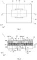
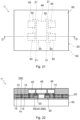
- Fig. 1 is a plan view of a semiconductor package 1 according to an embodiment.
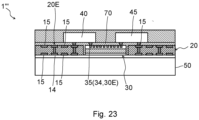
- Fig. 2 is a sectional view of the semiconductor package 1 in Fig. 1 taken along line A-A.
- the semiconductor package 1 has a first direction D1, a second direction D2, and a third direction D3.
- the first direction D1 and the second direction D2 are included in a plane direction of the semiconductor package 1.
- the first direction D1 is perpendicular to the second direction D2.
- the third direction D3 is the thickness direction of the semiconductor package 1.
- the third direction D3 is perpendicular to the first direction D1 and the second direction D2.
- the semiconductor package 1 includes an interposer 20, a redistribution layer chip 30, a first semiconductor element 40, a second semiconductor element 45, a support carrier 50, and a second mold resin layer 60.
- the redistribution layer chip 30 includes a redistribution element 31 and a first mold resin layer 32.
- the support carrier 50 supports the interposer 20 and the redistribution layer chip 30.
- the interposer 20 and the redistribution layer chip 30 are adjacent to each other above the support carrier 50 in the plane direction of the semiconductor package 1, or the first direction D1 in this example.
- the first semiconductor element 40 is stacked and mounted to the interposer 20 and the redistribution layer chip 30 in a direction that intersects with the direction in which the interposer 20 and the redistribution layer chip 30 are adjacent to each other, or the thickness direction of the semiconductor package 1 in this example, that is, the third direction D3. In other words, the first semiconductor element 40 overlaps the interposer 20 and the redistribution layer chip 30 when viewed in the third direction D3 in plan view.
- the second semiconductor element 45 is stacked and mounted to the interposer 20 and the redistribution layer chip 30 in the direction that intersects with the direction in which the interposer 20 and the redistribution layer chip 30 are adjacent to each other, or the thickness direction of the semiconductor package 1 in this example, that is, the third direction D3. In other words, the second semiconductor element 45 overlaps the interposer 20 and the redistribution layer chip 30 when viewed in the third direction D3 in plan view.
- the second mold resin layer 60 covers the interposer 20, the redistribution layer chip 30, the first semiconductor element 40, and the second semiconductor element 45.
- the interposer 20 illustrated includes a through-portion 21 that has a hole extending through the interposer 20 in the thickness direction, which is an example.
- the redistribution layer chip 30 is placed at the through-portion 21. Consequently, the redistribution layer chip 30 is adjacent to the interposer 20.
- the interposer 20 and the redistribution layer chip 30 extend in the first direction D1 and the second direction D2.
- the shape of the interposer 20 is not particularly limited.
- the interposer 20 may have a rectangular plate shape, and the redistribution layer chip 30 may be adjacent to the interposer 20 in the first direction D1 or the second direction D2.
- the redistribution layer chip 30 that is placed at the through-portion 21 may have a distance from the interposer 20 over the entire circumference of the redistribution layer chip 30.
- the distance between the redistribution layer chip 30 and the interposer 20 is 0.03 mm or more, may be 0.05 mm or more, or may be 0.1 mm or more.
- the distance between the redistribution layer chip 30 and the interposer 20 is 3.0 mm or less, may be 1.0 mm or less, or may be 0.5 mm or less.
- the distance between the redistribution layer chip 30 and the interposer 20 described herein is the minimum distance between a point on the outer circumference of the redistribution layer chip 30 and the through-portion 21.
- the shapes of the redistribution layer chip 30 and the through-portion 21 are not particularly limited. As illustrated in Fig. 1 , the redistribution layer chip 30 and the through-portion 21 may have a rectangular shape in plan view. The shape of the through-portion 21 in plan view may be larger than the redistribution layer chip 30 and may be similar to that of the redistribution layer chip 30.
- the redistribution layer chip 30 is one of multiple redistribution layer chips 30 that are cut out of a redistribution layer chip intermediate 300 (see Figs. 9 and Figs. 10 ) described later.
- the shape of the redistribution layer chip 30 is preferably a rectangular shape in consideration of ease of processing.
- the first semiconductor element 40 overlaps the interposer 20 and the redistribution layer chip 30 in plan view, in other words, when viewed in the third direction D3. Specifically, the first semiconductor element 40 overlaps the interposer 20 and the redistribution layer chip 30 and is mounted to the interposer 20 and the redistribution layer chip 30. The first semiconductor element 40 is electrically connected to both of the interposer 20 and the redistribution layer chip 30. Specifically, referring to Fig. 2 , the redistribution layer chip 30 includes a first conductive portion 30E that includes first wirings 35 that are electrically connected to the first semiconductor element 40. The first conductive portion 30E is included in a first redistribution layer 34 in the redistribution element 31.
- the interposer 20 includes a second conductive portion 20E that includes multiple through-electrodes 14 and second wirings 15.
- the second conductive portion 20E is included in a second redistribution layer 24 that is included in the interposer 20.
- one or more of the multiple through-electrodes 14 in the second conductive portion 20E are electrically connected to the first semiconductor element 40.
- the second semiconductor element 45 overlaps the interposer 20 and the redistribution layer chip 30 at a position that differs from that of the first semiconductor element 40 in plan view, in other words, when viewed in the third direction D3. Specifically, the second semiconductor element 45 overlaps the interposer 20 and the redistribution layer chip 30 and is mounted in this state.
- the second semiconductor element 45 is electrically connected to both of the interposer 20 and the redistribution layer chip 30.
- the first conductive portion 30E in the redistribution layer chip 30 includes the first wirings 35 that are electrically connected to the second semiconductor element 45.
- the second semiconductor element 45 is electrically connected to one or more of the multiple through-electrodes 14 of the second conductive portion 20E in the interposer 20.
- the first wirings 35 may electrically connect the first semiconductor element 40 and the second semiconductor element 45 to each other.
- the interposer 20 has a first surface 20A and a second surface 20B.
- the second surface 20B is opposite the first surface 20A.
- the through-electrodes 14 are located in through-holes 22A that extend from the first surface 20A to the second surface 20B.
- the interposer 20 includes an interposer insulating layer 22 in which the second conductive portion 20E (the second redistribution layer 24) that includes the through-electrodes 14 and the second wirings 15 is provided.
- the interposer insulating layer 22 includes the multiple through-holes 22A that extend in the thickness direction.
- the through-electrodes 14 are located in the through-holes 22A.
- the first semiconductor element 40 is electrically connected to the through-electrodes 14 in the second conductive portion 20E but may be electrically connected to, for example, an electrode that extends from the first surface 20A and that is located in a hole having a bottom.
- the second wirings 15 are imbedded in the interposer insulating layer 22. In other words, the second wirings 15 are covered by the interposer insulating layer 22.
- the second wirings 15 illustrated are embedded in the interposer insulating layer 22, and part of the second wirings 15 is exposed to the outside from the interposer insulating layer 22.
- the second wirings 15 may be connected to the semiconductor elements 40 and 45 at portions exposed to the outside from the interposer insulating layer 22.
- the second wirings 15 may be provided on the surface of the interposer insulating layer 22.
- the first surface 20A includes a surface of the interposer insulating layer 22 at one side in the thickness direction, surfaces of the through-electrodes 14 that are exposed from the through-holes 22A at one side in the thickness direction of the interposer insulating layer 22, and surfaces of the second wirings 15 that are exposed from the interposer insulating layer 22 at one side in the thickness direction of the interposer insulating layer 22.
- the second surface 20B includes a surface of the interposer insulating layer 22 at the other side in the thickness direction, surfaces of the through-electrodes 14 that are exposed from the through-holes 22A at the other side in the thickness direction of the interposer insulating layer 22, and surfaces of the second wirings 15 that are exposed from the interposer insulating layer 22 at the other side in the thickness direction of the interposer insulating layer 22.
- the through-portion 21 is formed in the interposer insulating layer 22.
- the multiple through-holes 22A are formed at portions around the through-portion 21 in the interposer insulating layer 22. Accordingly, the multiple through-electrodes 14 are located around the through-portion 21 in the interposer insulating layer 22.
- the second wirings 15 are located around the through-portion 21 in the interposer insulating layer 22. The through-electrodes 14 and the second wirings 15 may be electrically connected.
- the redistribution layer chip 30 has a first surface 30A and a second surface 30B.
- the second surface 30B is opposite the first surface 30A.
- the first surface 30A of the redistribution layer chip 30 faces in the same direction as the first surface 20A of the interposer 20.
- the second surface 30B of the redistribution layer chip 30 faces in the same direction as the second surface 20B of the interposer 20.
- the first semiconductor element 40 and the second semiconductor element 45 overlap the first surface 20A of the interposer 20 and the first surface 30A of the redistribution layer chip 30.
- the first semiconductor element 40 and the second semiconductor element 45 are mounted to the first surface 20A of the interposer 20 and the first surface 30A of the redistribution layer chip 30.
- Portions of the first wirings 35 in the first conductive portion 30E described above are located at the first surface 30A.
- the portions of the first wirings 35 that are located at the first surface 30A are connected to the semiconductor elements 40 and 45.
- the support carrier 50 faces the first semiconductor element 40 and the second semiconductor element 45 with the interposer 20 and the redistribution layer chip 30 interposed therebetween.
- the support carrier 50 supports the interposer 20 and the redistribution layer chip 30.
- the second surface 20B of the interposer 20 faces the support carrier 50.
- the interposer 20 is formed above the support carrier 50 such that the second surface 20B is in contact with a release layer 51.
- the second surface 30B is joined to the support carrier 50 with the release layer 51 interposed therebetween, and consequently, the redistribution layer chip 30 is mounted to the support carrier 50.
- the support carrier 50 is separable from the interposer 20 and the redistribution layer chip 30.
- the support carrier 50 is separated from the interposer 20 and the redistribution layer chip 30 together with the release layer 51.
- the second mold resin layer 60 covers the interposer 20 and the redistribution layer chip 30 and is mounted to the interposer 20 and the redistribution layer chip 30. Specifically, the second mold resin layer 60 is joined to the first surface 20A of the interposer 20 and the first surface 30A of the redistribution layer chip 30. The second mold resin layer 60 is joined to the first semiconductor element 40 and the second semiconductor element 45 and holds the first semiconductor element 40 and the second semiconductor element 45. This enables the interposer 20, the redistribution layer chip 30, the first semiconductor element 40, and the second semiconductor element 45 that are connected as a single body to be maintained even in the case where the support carrier 50 is separated from the interposer 20 and the redistribution layer chip 30.
- the interposer 20 includes the interposer insulating layer 22 and the second redistribution layer 24.
- the second redistribution layer 24 includes the second conductive portion 20E, and the second conductive portion 20E includes the through-electrodes 14 and the second wirings 15.
- the through-electrodes 14 and the second wirings 15 are conductive.
- the interposer 20 may include pads 16 that are provided at the first surface 20A.
- the interposer 20 may include an insulating layer and a wiring provided on the first surface 20A although not illustrated.
- the interposer insulating layer 22 may be composed of insulating resin.
- the insulating resin of which the interposer insulating layer 22 is composed may include polyimide, epoxy resin, acryl resin, or a combination of two or more of these.
- the interposer insulating layer 22 is composed of polyimide.
- the interposer insulating layer 22 may be a glass substrate, a quartz substrate, a sapphire substrate, a silicon substrate, a silicon carbide substrate, an alumina (Al2O3) substrate, an aluminum nitride (AIN) substrate, a zirconium oxide (ZrO2) substrate, a lithium niobate substrate, a tantalum niobate substrate, or a multiplayer substrate of these.
- the interposer insulating layer 22 may include a portion of a substrate composed of a conductive material such as an aluminum substrate, or a stainless steel substrate.
- the thickness of the interposer insulating layer 22 is 0.01 mm or more, may be 0.1 mm or more, or may be 0.2 mm or more.
- the thickness of the interposer insulating layer 22 is 2.0 mm or less, may be 1.5 mm or less, or may be 1.0 mm or less.
- the through-electrodes 14 extend from one surface of the interposer insulating layer 22 to the other surface in the thickness direction in the through-holes 22A of the interposer insulating layer 22.
- the through-electrodes 14 may be located over the entire region of the through-holes 22A. That is, the through-electrodes 14 may be so-called filled-vias that fill the through-holes 22A.
- the through-electrodes 14 may or may not fill the through-holes 22A.
- the through-electrodes 14 may include multiple layers.
- the through-electrodes 14 may include first layers that are located on side surfaces of the through-holes 22A and second layers that are located on the first layers. The second layers may extend to the centers of the through-holes 22A in plan view.
- the first layers are formed on the side surfaces of the through-holes 22A by using a physical film formation method such as a spattering method or a vapor deposition method.
- the thicknesses of the first layers are 0.05 ⁇ m or more.
- the thicknesses of the first layers are 1.0 ⁇ m or less.
- Other layers may be provided between the first layers and the side surfaces of the through-holes 22A.
- the materials of the first layers can be metal such as titanium, chromium, nickel, or copper, an alloy of these, or a stack of these.
- the second layers may contain copper as a main component.
- the second layers may contain copper in an amount of 80% or more by mass.
- the second layers may contain metal such as gold, silver, platinum, rhodium, tin, aluminum, nickel, or chromium or an alloy of these.
- the second layers are formed on the first layers by using an electroplating method.
- the second wirings 15 include conductive layers. Examples of the materials of the second wirings 15 can include the materials described for the through-electrodes 14. For example, the thicknesses of the second wirings 15 are 0.5 ⁇ m or more or may be 1.0 ⁇ m or more. For example, the thicknesses of the second wirings 15 are 10.0 ⁇ m or less or may be 5.0 ⁇ m or less. For example, the line widths of the second wirings 15 are 5 ⁇ m or more or may be 10 ⁇ m or more. For example, the line widths of the second wirings 15 are 30 ⁇ m or less or may be 20 ⁇ m or less.
- the pads 16 contain conductive layers.
- the pads 16 may be located above the through-electrodes 14 at the first surface 20A.
- Examples of the materials of the pads 16 can include the materials described for the through-electrodes 14.
- the thicknesses of the pads 16 are 0.5 ⁇ m or more or may be 1.0 ⁇ m or more.
- the thicknesses of the pads 16 are 10.0 ⁇ m or less or may be 5.0 ⁇ m or less.
- Fig. 3 is an enlarged sectional view of the redistribution layer chip 30.
- the redistribution layer chip 30 includes the redistribution element 31, the first mold resin layer 32, and an adhesive layer 36.
- the redistribution element 31 includes an insulating layer 33 that has insulation properties and the first redistribution layer 34 that is embedded in the insulating layer 33.
- the redistribution element 31 includes the insulating layer 33 that has the insulation properties and the first redistribution layer 34 that is covered by the insulating layer 33.
- the redistribution layer chip 30 is used for redistribution and is accordingly referred to as the "redistribution layer" chip.
- the redistribution layer chip 30 may be simply referred to as a wiring layer chip, and the redistribution element 31 may be simply referred to as a wiring element.
- the redistribution element 31 has a first surface 31A and a second surface 31B opposite the first surface 31A.
- the first surface 31A forms a surface that the first semiconductor element 40 and the second semiconductor element 45 overlap. That is, in the state of Fig. 2 , the first surface 31A forms the first surface 30A of the redistribution layer chip 30.
- the first mold resin layer 32 is mounted to the second surface 31B.
- the adhesive layer 36 is mounted to a surface opposite the surface of the first mold resin layer 32 that is mounted to the second surface 31B of the redistribution element 31.
- the adhesive layer 36 forms the second surface 30B of the redistribution layer chip 30.
- the redistribution layer chip 30 may include pads 37 that are provided at the first surface 31A.
- the first redistribution layer 34 includes the first conductive portion 30E that includes the first wirings 35 described above.
- at least the portions of the first wirings 35 in the first conductive portion 30E are located at the first surface 31A of the redistribution element 31.
- at least the portions of the first wirings 35 form the first surface 31A.
- At least the portions of the first wirings 35 in the first conductive portion 30E that are located at the first surface 31A are connected to the semiconductor elements 40 and 45.
- the insulating layer 33 may include polyimide, epoxy resin, acryl resin, or a combination of two or more of these.
- the thickness of the insulating layer 33 is 3 ⁇ m or more or may be 5 ⁇ m or more.
- the thickness of the insulating layer 33 is 20 ⁇ m or less or may be 10 ⁇ m or less.
- Examples of the material of the first conductive portion 30E that includes the first wirings 35 can include the materials described for the through-electrodes 14.
- the thicknesses of the first wirings 35 are 0.5 ⁇ m or more or may be 1 ⁇ m or more.
- the thicknesses of the first wirings 35 are 5 ⁇ m or less or may be 3 ⁇ m or less.
- the line widths of the first wirings 35 are 10 ⁇ m or less.
- the line widths of the first wirings 35 may be 5 ⁇ m or less, may be 3 ⁇ m or less, or may be 2 ⁇ m or less.
- the line widths of the first wirings 35 may be less than the line widths of the second wirings 15 of the interposer 20.
- the minimum value of the line widths of the first wirings 35 is 1/2 or less, may be 1/5 or less, or may be 1/10 or less of the minimum value of the line widths of the second wirings 15 of the interposer 20.
- the multiple first wirings 35 may be provided in a line-and-space pattern.
- the line widths of the first wirings 35 and the distances (spaces) between the first wirings 35 adjacent to each other may be equal to each other or may differ from each other.
- the distances between the first wirings 35 adjacent to each other may be 1 ⁇ m or more and 5 ⁇ m or less, may be 1 ⁇ m or more and 3 ⁇ m or less, or may be 1 ⁇ m or more and 2 ⁇ m or less.
- the aspect ratios (thicknesses/line widths) of the first wirings 35 may be 1 or more and 4 or less or may be 1 or more and 2.5 or less.
- Fig. 4 is a sectional view of the redistribution layer chip 30 in Fig. 3 taken along line B-B.
- the first wirings 35 linearly extend in the second direction D2.
- the first redistribution layer 34 includes the multiple first wirings 35, and the multiple first wirings 35 are formed in parallel with each other in the line-and-space pattern.
- Each first wiring 35 has a section that has a rectangular shape in the direction perpendicular to the longitudinal direction, and only one side of four sides of the rectangular shape is exposed to the outside from the insulating layer 33.
- the surface of each first wiring 35 that is exposed to the outside from the insulating layer 33 forms the first surface 31A.
- the pattern in which the first wirings 35 are formed is not particularly limited.
- the first redistribution layer 34 may include a wiring that is completely embedded in, in other words, covered by the insulating layer 33.
- the first conductive portion 30E in the first redistribution layer 34 may include a through-electrode.
- the first conductive portion 30E in the first redistribution layer 34 may include a wiring that is located at the second surface 31B.
- the pads 37 include conductive layers.
- the pads 37 may be located above the first wirings 35 on the first surface 31A.
- Examples of the materials of the pads 37 can include the materials described for the through-electrodes 14.
- the thicknesses of the pads 37 are 0.5 ⁇ m or more or may be 1.0 ⁇ m or more.
- the thicknesses of the pads 37 are 10.0 ⁇ m or less or may be 5.0 ⁇ m or less.
- the first mold resin layer 32 contains resin.
- the resin that is contained in the first mold resin layer 32 may include polyimide, epoxy resin, acryl, bismaleimide, polybenzoxazole, benzocyclobutene, or a combination of two or more of these.
- the first mold resin layer 32 is provided to inhibit the redistribution element 31 from deforming.
- the first mold resin layer 32 may have at least any one of characteristics (1) to (4) described below to preferably inhibit the redistribution element 31 from deforming.
- the thermal expansion coefficient of the first mold resin layer 32 and the thermal expansion coefficient of the insulating layer 33 are measured in accordance with JISK7197:2012. That is, in the present specification, the thermal expansion coefficient means the linear expansion coefficient that is measured in accordance with JISK7197:2012.
- the Young's modulus of the first mold resin layer 32 and the Young's modulus of the insulating layer 33 are specified in a manner in which the mechanical characteristics of the first mold resin layer 32 and the insulating layer 33 are measured by using a nanoindentation method.
- the bending stiffness of the first mold resin layer 32 and the bending stiffness of the insulating layer 33 are calculated in a manner in which the Young's moduli of the first mold resin layer 32 and the insulating layer 33 are specified by using the nanoindentation method described above, and the sectional shapes of the first mold resin layer 32 and the insulating layer 33 are specified.
- the Young's moduli are measured by using the nanoindentation method described above through procedures described below.
- the first mold resin layer 32 and the insulating layer 33 are placed on a measurement device "TI950 Tribolndenter" made by BRUKER.
- TI950 Tribolndenter made by BRUKER.
- the redistribution layer chip 30 is cut and is placed on the measurement device described above.
- the redistribution layer chip 30 before incorporation is placed on the measurement device described above.
- the nanoindentation method starts for measurement at a side surface of the first mold resin layer 32 or the insulating layer 33.
- an indenter is pressed against the side surface of the first mold resin layer 32 or the insulating layer 33 at any intermediate position in the thickness direction for 10 seconds up to a depth of 100 nm in a plane direction, is held in this state for 5 seconds, and is subsequently returned to a depth of 0 nm for 10 seconds.
- the first mold resin layer 32 and the insulating layer 33 are pressed separately. Consequently, the Young's modulus of each target to be measured is calculated.
- the indenter described above is a diamond indenter (Berkovich indenter TI-0039) at a face angle of 142.3°.
- the thermal expansion coefficient (the linear expansion coefFicient) of the first mold resin layer 32 may be 2 ppm/°C or more and 12 ppm/°C or less or may be 5 ppm/°C or more and 9 ppm/°C or less.
- the linear expansion coefficient of the first mold resin layer 32 may be lower than the linear expansion coefficient of the insulating layer 33 in the perspective that the redistribution element 31 is inhibited from deforming as described above.
- Examples of the insulating layer 33 may include polyimide, epoxy resin, acryl resin, or a combination of two or more of these as described above.
- Examples of the resin that is contained in the first mold resin layer 32 may include polyimide, epoxy resin, acryl resin, bismaleimide, polybenzoxazole, benzocyclobutene, or a combination of two or more of these.
- a relationship of the linear expansion coefficient of polyimide > the linear expansion coefficient of acryl > the linear expansion coefficient of epoxy is typically satisfied. Accordingly, in the case where the linear expansion coefficient of the first mold resin layer 32 is lower than the linear expansion coefficient of the insulating layer 33, for example, in the case where the first mold resin layer 32 contains polyimide, the insulating layer 33 preferably contains polyimide.
- the amount of polyimide molecules that are contained in the first mold resin layer 32 may be larger than the amount of polyimide molecules that are contained in the insulating layer 33 in order to reduce the linear expansion coefficient of the first mold resin layer 32 to a coefficient lower than the linear expansion coefficient of the insulating layer 33. As the amount of the molecules increases, the movement of the molecules is restricted, and the linear expansion coefficient tends to decrease. In the case where the first mold resin layer 32 and the insulating layer 33 contain the same resin, the amount of resin molecules that are contained in the first mold resin layer 32 may be larger than the amount of resin molecules that are contained in the insulating layer 33 when the linear expansion coefficient of the first mold resin layer 32 is reduced to the coefficient lower than the linear expansion coefficient of the insulating layer 33. In the case where the first mold resin layer 32 and the insulating layer 33 contain the same resin, the adhesion strength between the first mold resin layer 32 and the insulating layer 33 can be improved.
- the Young's modulus of the first mold resin layer 32 may be 12 GPa or more and 30 GPa or less or may be 18 GPa or more and 22 GPa or less.
- the Young's modulus of the first mold resin layer 32 may be more than the Young's modulus of the insulating layer 33 in the perspective that the redistribution element 31 is inhibited from deforming as described above.
- a relationship of the Young's modulus of polyimide > the Young's modulus of acryl > the Young's modulus of epoxy is typically satisfied.
- the insulating layer 33 preferably contains polyimide.
- the amount of polyimide molecules that are contained in the first mold resin layer 32 may be larger than the amount of polyimide molecules that are contained in the insulating layer 33 in order that the Young's modulus of the first mold resin layer 32 is more than the Young's modulus of the insulating layer 33.
- the first mold resin layer 32 may contain a filler that is dispersed in resin such as epoxy resin.
- the filler may be particles such as silica or alumina particles.
- the filler may be silicon oxide particles or silicon nitride particles.
- the silicon oxide or the silicon nitride may contain fluorine or nitrogen.
- the filler may be carbon black particles.
- the semiconductor package 1 is inhibited from deforming due to differences in the physical properties of these, flatness is easily maintained, and the size of the semiconductor package 1 is easily increased.
- the first mold resin layer 32 and the insulating layer 33 in the redistribution layer chip 30 and the interposer insulating layer 22 in the interposer 20 may contain the same resin.
- the thermal conductivity of the filler is preferably more than the thermal conductivity of the resin in which the filler is dispersed in the perspective of an improvement in the heat dissipation.
- the filler may be composed of an inorganic material.
- the color of the filler may be black. In the case where the color of the first mold resin layer 32 is black because of the black filler, for example, light can be inhibited from passing through the redistribution layer chip.
- the thickness of the first mold resin layer 32 is 5 ⁇ m or more or may be 10 ⁇ m or more.
- the thickness of the first mold resin layer 32 is 50 ⁇ m or less or may be 20 ⁇ m or less.
- the first mold resin layer 32 may have a through-hole for providing a through-electrode.
- the redistribution layer chip 30 is mounted to the support carrier 50 with the first mold resin layer 32 connected to the support carrier 50. Specifically, the first mold resin layer 32 is connected to the support carrier 50 with the adhesive layer 36 and the release layer 51 interposed therebetween, and the adhesive layer 36 is joined to the release layer 51 in this state. Consequently, the redistribution layer chip 30 is mounted to the support carrier 50.
- the adhesive layer 36 has heat-sensitive adhesiveness, or photosensitive adhesiveness, or pressure-sensitive adhesiveness.
- the adhesive layer 36 may be composed of thermoplastic polyimide, which is a material that has the heat-sensitive adhesiveness. As long as the first mold resin layer 32 and the support carrier 50 are joined, the adhesive layer 36 may not be provided.
- a NCF (Non Conductive Film) or a NCP (Non Conductive Paste) for mounting a semiconductor may be used as the adhesive layer 36.
- the adhesive layer 36 is heated and is subsequently cooled, and consequently, the redistribution layer chip 30 and the support carrier 50 can be stuck to each other by using the NCF or the NCP.
- the thickness of the adhesive layer 36 is 5 ⁇ m or more or may be 10 ⁇ m or more.
- the thickness of the adhesive layer 36 is 100 ⁇ m or less or may be 30 ⁇ m or less.
- Fig. 5 is a sectional view of the redistribution layer chip 30 before the redistribution layer chip 30 is incorporated as a portion of the semiconductor package 1.
- the redistribution layer chip 30 before incorporation (referred to below as a pre-incorporation redistribution layer chip 30' in some cases) illustrated in Fig. 5 may include a chip carrier 38 in contact with the first surface 31A of the redistribution element 31.
- the chip carrier 38 may be mounted to the first surface 31A with a release layer 39 interposed therebetween.
- the pre-incorporation redistribution layer chip 30' before incorporation as the portion of the semiconductor package 1 the first wirings 35 that are located at the first surface 31A are covered and are protected by the chip carrier 38.
- the chip carrier 38 may include a glass substrate, a quartz substrate, a sapphire substrate, a resin substrate, a silicon substrate, a silicon carbide substrate, an alumina (Al2O3) substrate, an aluminum nitride (AIN) substrate, a zirconium oxide (ZrO2) substrate, a lithium niobate substrate, or a tantalum niobate substrate.
- the resin substrate may contain an organic material.
- the resin substrate may contain epoxy resin, polyethylene, or polypropylene.
- the release layer 39 is joined to the first surface 31A of the redistribution element 31 and is joined to the chip carrier 38.
- the release layer 39 can be separated from the portions of the first wirings 35 that form the first surface 31A and the insulating layer 33 and may be separated, for example, by being heated.
- the release layer 39 may contain thermoplastic resin.
- the release layer may be a polyimide resin release layer that can be separated by using about 355 nm laser light.
- the chip carrier 38 is also separated.
- the thickness of the chip carrier 38 is 700 ⁇ m or more or may be 1000 ⁇ m or more.
- the thickness of the chip carrier 38 is 2000 ⁇ m or less or may be 1200 ⁇ m or less.
- the thickness of the release layer 39 is 0.3 ⁇ m or more or may be 1 ⁇ m or more.
- the thickness of the release layer 39 is 30 ⁇ m or less or may be 100 ⁇ m or less.
- the redistribution layer chip 30 is incorporated as the portion of the semiconductor package 1, the chip carrier 38 and the release layer 39 are removed from the pre-incorporation redistribution layer chip 30'.
- the redistribution layer chip 30 is joined to the release layer 51 with the adhesive layer 36 interposed therebetween and is consequently mounted to the support carrier 50.
- the redistribution layer chip 30 is placed with the adhesive layer 36 being in contact with the release layer 51. Subsequently, the adhesive layer 36 may be heated, and consequently, the adhesive layer 36 and the release layer 51 may be joined.
- the first semiconductor element 40 includes a transistor composed of a semiconductor such as silicon.
- Examples of the first semiconductor element 40 include a CPU, a GPU, a FPGA, a sensor, and a memory.
- the first semiconductor element 40 may be a chiplet in which semiconductor elements such as a CPU, a GPU, a FPGA, a sensor, and a memory are divided for every function.
- the first semiconductor element 40 may include multiple substrates that are stacked.
- the first semiconductor element 40 is electrically connected to the interposer 20 with the pads 16 interposed therebetween.
- a bump may be provided between the pads 16 of the interposer 20 and the first semiconductor element 40.
- the first semiconductor element 40 is electrically connected to the first wirings 35 in the first conductive portion 30E of the redistribution layer chip 30 with the pads 37 interposed therebetween.
- a bump may be provided between the pads 37 of the redistribution layer chip 30 and the first semiconductor element 40.
- the second semiconductor element 45 includes a transistor composed of a semiconductor such as silicon. Examples of the second semiconductor element 45 include a CPU, a GPU, a FPGA, a sensor, and a memory.
- the second semiconductor element 45 may be a chiplet in which semiconductor elements such as a CPU, a GPU, a FPGA, a sensor, and a memory are divided for every function.
- the second semiconductor element 45 may include multiple substrates that are stacked.
- the shape, function, and performance of the second semiconductor element 45 for example, may be the same as the shape, function, and performance of the first semiconductor element 40 or may differ therefrom.
- the second semiconductor element 45 is electrically connected to the interposer 20 with the pads 16 interposed therebetween.
- a bump may be provided between the pads 16 of the interposer 20 and the second semiconductor element 45.
- the second semiconductor element 45 is electrically connected to the first wirings 35 of the redistribution layer chip 30 with the pads 37 interposed therebetween.
- a bump may be provided between the pads 37 of the redistribution layer chip 30 and the second semiconductor element 45.
- the support carrier 50 supports the interposer 20 and the redistribution layer chip 30.
- the support carrier 50 is separable from the interposer 20 and the redistribution layer chip 30.
- the release layer 51 is also separated.
- the through-electrodes 14 and the second wirings 15 are exposed to the outside. This enables the through-electrodes 14 and the second wirings 15 to be electrically connected to, for example, another semiconductor package or a wiring substrate.
- the support carrier 50 has a size that covers the whole of a combination of the interposer 20 and the redistribution layer chip 30.
- An example of the shape of the support carrier 50 may be a rectangular shape.
- the support carrier 50 supports the single combination of the interposer 20 and the redistribution layer chip 30 but may support multiple combinations of the interposers 20 and the redistribution layer chips 30.
- the semiconductor package 1 is formed by being cut out of a support carrier substrate 50P (see Fig. 16A ) that supports the multiple combinations of the interposers 20 and the redistribution layer chips 30 described later.
- the support carrier 50 is a portion of the support carrier substrate 50P and is cut out of the support carrier substrate 50P.
- the interposer 20, the redistribution layer chip 30, the semiconductor elements 40 and 45, and the second mold resin layer 60 corresponding thereto are mounted on the support carrier 50 cut.
- the support carrier 50 may include a glass substrate, a quartz substrate, a sapphire substrate, a resin substrate, a silicon substrate, a silicon carbide substrate, an alumina (Al2O3) substrate, an aluminum nitride (AIN) substrate, a zirconium oxide (ZrO2) substrate, a lithium niobate substrate, or a tantalum niobate substrate.
- the resin substrate may contain an organic material.
- the resin substrate may contain epoxy resin, polyethylene, or polypropylene.
- the thickness of the support carrier 50 is 100 ⁇ m or more, may be 200 ⁇ m or more, or may be 500 ⁇ m or more.
- the thickness of the support carrier 50 is 2 mm or less, may be 1.5 mm or less, or may be 1 mm or less.
- the release layer 51 is joined to the second surface 20B of the interposer 20 and the second surface 30B of the redistribution layer chip 30 and is joined to the support carrier 50.
- the release layer 51 can be separated from the second surface 20B of the interposer 20 and the second surface 30B of the redistribution layer chip 30 and may be separated, for example, by being heated.
- the release layer 51 may contain thermoplastic resin.
- the thickness of the release layer 51 is 0.3 ⁇ m or more or may be 1 ⁇ m or more.
- the thickness of the release layer 51 is 30 ⁇ m or less or may be 50 ⁇ m or less.
- the second mold resin layer 60 contains resin, and examples of the resin that is contained in the second mold resin layer 60 may include polyimide, epoxy resin, acryl, bismaleimide, polybenzoxazole, benzocyclobutene, or a combination of two or more of these.
- the second mold resin layer 60 may contain thermosetting resin.
- the resin that is contained in the second mold resin layer 60 may be thermosetting epoxy resin.
- the second mold resin layer 60 covers the interposer 20, the redistribution layer chip 30, the first semiconductor element 40, and the second semiconductor element 45.
- the second mold resin layer 60 is joined to the interposer 20, the redistribution layer chip 30, the first semiconductor element 40, and the second semiconductor element 45. Consequently, the second mold resin layer 60 is mounted to the interposer 20 and the redistribution layer chip 30 and holds the first semiconductor element 40 and the second semiconductor element 45 in this state.
- the second mold resin layer 60 may cover the whole of the first semiconductor element 40 and the second semiconductor element 45.
- the second mold resin layer 60 may cover the first semiconductor element 40 and the second semiconductor element 45 with portions thereof exposed.
- the second mold resin layer 60 may fill a gap between the through-portion 21 in the interposer 20 and the redistribution layer chip 30.
- the second mold resin layer 60 may be joined to side surfaces of the redistribution layer chip 30 and the through-portion 21.
- the thickness of the second mold resin layer 60 is 30 ⁇ m or more or may be 100 ⁇ m or more.
- the thickness of the second mold resin layer 60 is 300 ⁇ m or less or may be 600 ⁇ m or less.
- the thickness of the second mold resin layer 60 is equal to a distance from the surface in contact with the interposer 20 to the opposite surface.
- a method of manufacturing the semiconductor package 1 according to the present embodiment will now be described. As for the manufacturing method described later, a procedure for manufacturing the redistribution layer chip intermediate 300 that is used as the base material of the redistribution layer chip 30 will be first described. A procedure for manufacturing the redistribution layer chip 30 that is manufactured from the redistribution layer chip intermediate 300 will be next described. A procedure for manufacturing the semiconductor package 1 that is manufactured by using the redistribution layer chip 30 will be then described.
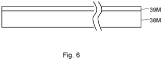
- a chip carrier substrate 38M is prepared.
- a release layer 39M is formed on the chip carrier substrate 38M.
- the redistribution layer chip 30 is one of multiple chips that are cut out of the redistribution layer chip intermediate 300.
- the release layer 39M corresponds to a portion that includes the release layer 39 before the release layer 39 is cut as a component of the redistribution layer chip 30.
- the chip carrier substrate 38M may be a glass substrate or a silicon substrate (a wafer).
- the shape of the chip carrier substrate 38M may be a circular shape such as a wafer.
- the diameter of the chip carrier substrate 38M is 100 mm or more, may be 150 mm or more, or may be 200 mm or more.
- the diameter of the chip carrier substrate 38M is 400 mm or less, may be 350 mm or less, or may be 300 mm or less.
- the release layer 39M may contain thermoplastic resin.
- the release layer 39M may be formed in a manner in which a thermoplastic resin film is joined to the chip carrier substrate 38M.
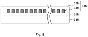
- multiple first redistribution layers 34 are formed on the release layer 39M.
- the first redistribution layers 34 are formed along the chip carrier substrate 38M that has a circular shape.
- the multiple first redistribution layers 34 illustrated in Fig. 7A and Fig. 7B include wirings that form the multiple redistribution layer chips 30.
- the multiple first redistribution layers 34 are also referred to as a redistribution layer group 34M.
- the redistribution layer group 34M may be formed by using photolithography. In this case, for example, a conductive layer composed of, for example, copper is provided on the chip carrier substrate 38M.
- a photosensitive resist film is provided on the conductive layer.
- the resist film is exposed to light in a desired pattern that corresponds to the first redistribution layers 34 by using an exposure device.
- the resist film is removed.
- the conductive layer is etched, and consequently, the redistribution layer group 34M is formed.
- the redistribution layer group 34M is covered by an insulating layer 33M.
- the insulating layer 33M corresponds to a portion that includes the insulating layer 33 before the insulating layer 33 is cut as a component of the redistribution layer chip 30.
- the insulating layer 33M may be formed in a manner in which a material composed of polyimide, epoxy resin, acryl resin, or a combination of two or more of these is hardened.
- the insulating layer 33M covers surfaces of the redistribution layer group 34M other than the surface in contact with the release layer 39M such that the redistribution layer group 34M is not exposed.
- the redistribution layer group 34M and the insulating layer 33M form a redistribution element portion 31M.
- the redistribution element portion 31M corresponds to a portion that includes the redistribution element 31 before the redistribution element 31 is cut as a component of the redistribution layer chip 30.
- the insulating layer 33M is covered by a first mold resin layer portion 32M.
- the first mold resin layer portion 32M corresponds to a portion that includes the first mold resin layers 32 before each first mold resin layer 32 is cut as a component of the redistribution layer chip 30.
- the first mold resin layer portion 32M may be formed in a manner in which a material composed of polyimide, epoxy resin, acryl, bismaleimide, polybenzoxazole, benzocyclobutene, or a combination of two or more of these is hardened.
- the first mold resin layer portion 32M is covered by an adhesive layer 36M.
- the adhesive layer 36M corresponds to a portion that includes the adhesive layers 36 before each adhesive layer 36 is cut as a component of the redistribution layer chip 30.
- the adhesive layer 36M may be composed of thermoplastic polyimide that has the heat-sensitive adhesiveness.
- the redistribution layer chip intermediate 300 is manufactured through the procedures described above.
- the redistribution layer chip intermediate 300 includes the redistribution element portion 31M, the first mold resin layer portion 32M that contains resin, and the chip carrier substrate 38M.
- the redistribution element portion 31M includes the insulating layer 33M that has the insulation properties and the multiple first redistribution layers 34 that are embedded in, in other words, covered by the insulating layer 33M and has a first surface (a lower surface in Fig. 9A ) and a second surface (an upper surface in Fig. 9A ) opposite the first surface.
- the first redistribution layers 34 include first conductive portions 30E that include the first wirings 35 that are at least partly located at the first surface.
- the first mold resin layer portion 32M is mounted to the second surface of the redistribution element portion 31M.
- the chip carrier substrate 38M is connected to the first surface of the redistribution element portion 31M with the release layer 39M interposed therebetween and supports the redistribution element portion 31M and the first mold resin layer portion 32M.
- the redistribution layer chip intermediate 300 further includes the adhesive layer 36M that is mounted to the first mold resin layer portion 32M and the release layer 39M that is provided between the redistribution element portion 31M and the chip carrier substrate 38M.
- the redistribution layer chip intermediate 300 is cut into multiple pieces. Consequently, the multiple redistribution layer chips 30 are cut out of the redistribution layer chip intermediate 300. Consequently, the redistribution layer chip 30 is manufactured.
- the pre-incorporation redistribution layer chip 30' is illustrated in Fig. 10A and Fig. 10B .
- the redistribution layer chip 30 from which the chip carrier 38 and the release layer 39 are removed is illustrated.
- the redistribution layer chip 30 is incorporated as a portion of the semiconductor package 1 after the chip carrier 38 and the release layer 39 are removed.
- a multilayer body that includes the redistribution element portion 31M and the first mold resin layer portion 32M may be cut into multiple pieces after the chip carrier substrate 38M and the release layer 39M are separated from the redistribution element portion 31M although this is not illustrated.
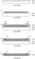
- the support carrier substrate 50P is prepared.
- the area of the support carrier substrate 50P is 0.5 m 2 or more, may be 1.0 m 2 or more, may be 2.0 m 2 or more, or may be 3.0 m 2 or more.
- a release layer 51M is formed on the support carrier substrate 50P.
- the release layer 51M corresponds to a portion that includes the release layer 51 before the release layer 51 is cut as a component of the semiconductor package 1.
- an interposer layer 20M is formed above the support carrier substrate 50P.
- the interposer layer 20M corresponds to a portion that includes multiple interposers 20 before each interposer 20 is cut as a component of the semiconductor package 1.
- the interposer layer 20M includes multiple through-portions 21.
- the multiple redistribution layer chips 30 are prepared.
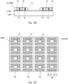
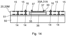
- the redistribution layer chips 30 are placed at the multiple through-portions 21. Specifically, as illustrated in Fig. 13A and Fig. 13B , the redistribution layer chips 30 are placed so as to be adjacent to the respective interposers 20 of the multiple interposers 20 that are included in the interposer layer 20M, and the redistribution layer chips 30 are mounted to the support carrier substrate 50P.
- the redistribution layer chips 30 are joined to the release layer 51M with the adhesive layers 36 interposed therebetween and are consequently mounted to the support carrier substrate 50P.
- the redistribution layer chips 30 are placed with the adhesive layers 36 being in contact with the release layer 51M.
- the adhesive layers 36 may be heated, and consequently, the adhesive layers 36 and the release layer 51M may be joined.
- the redistribution layer chips 30 are mounted to the support carrier substrate 50P as described above, and consequently, a semiconductor package intermediate 1M illustrated in Fig. 13A and Fig. 13B is manufactured.
- the semiconductor package intermediate 1M includes the interposers 20, the redistribution layer chips 30 adjacent to the interposers 20, and the support carrier substrate 50P that supports the interposers 20 and the redistribution layer chips 30. More specifically, the semiconductor package intermediate 1M includes the interposer layer 20M that includes the multiple interposers 20, the multiple redistribution layer chips 30 adjacent to the multiple interposers 20, and the support carrier substrate 50P that supports the multiple interposers 20 and the redistribution layer chips 30.
- the pads 16 are provided at the first surfaces 20A of the interposers 20.
- the pads 16 are electrically connected to the through-electrodes 14.
- the pads 37 are formed at the first surfaces 31A that are formed by portions of the first wirings 35 of the redistribution layer chips 30.
- the pads 37 are electrically connected to the first wirings 35.
- the first semiconductor elements 40 and the second semiconductor elements 45 are mounted so as to overlap the interposers 20 and the redistribution layer chips 30.
- multiple combinations of the first semiconductor elements 40 and the second semiconductor elements 45 overlap the respective interposers 20 and the respective redistribution layer chips 30.
- the first semiconductor elements 40 are electrically connected to the through-electrodes 14 of the interposers 20 with the pads 16 interposed therebetween.
- the first semiconductor elements 40 are electrically connected to the first wirings 35 of the redistribution layer chips 30 with the pads 37 interposed therebetween.
- the second semiconductor elements 45 are electrically connected to the through-electrodes 14 of the interposers 20 with the pads 16 interposed therebetween.
- the second semiconductor elements 45 are electrically connected to the first wirings 35 of the redistribution layer chips 30 with the pads 37 interposed therebetween.
- a second mold resin layer portion 60M is provided.
- the second mold resin layer portion 60M corresponds to a portion that includes the second mold resin layer 60 before the second mold resin layer 60 is cut as a component of each redistribution layer chip 30. Consequently, a semiconductor package block that includes the multiple semiconductor packages 1 is formed.
- the semiconductor packages 1 are cut out of the block described above.
- the second mold resin layer portion 60M is joined to the first surfaces 20A of the multiple interposers 20 and the first surfaces 30A of the redistribution layer chips 30.
- the second mold resin layer portion 60M is joined to the multiple first semiconductor elements 40 and the second semiconductor elements 45 and holds the multiple first semiconductor elements 40 and the second semiconductor elements 45. Consequently, even in the case where the support carrier 50 is separated from the interposers 20 and the redistribution layer chips 30 after the semiconductor packages 1 are cut out of the block, the second mold resin layer 60 maintains the interposers 20, the redistribution layer chips 30, the first semiconductor elements 40, and the second semiconductor elements 45 that are connected as respective bodies.
- the second mold resin layer portion 60M may be formed in a manner in which a softened material is hardened.
- the second mold resin layer portion 60M may be formed in a manner in which a liquid material is solidified.
- Each semiconductor package 1 described above includes the interposer 20, the redistribution layer chip 30 adjacent to the interposer 20, and the semiconductor elements 40 and 45 that overlap the interposer 20 and the redistribution layer chip 30.
- the redistribution layer chip 30 includes the redistribution element 31 that has the first surface 31A overlapping the semiconductor elements 40 and 45, and the first mold resin layer 32 that is mounted to the second surface 31B of the redistribution element 31 opposite the surface overlapping the semiconductor elements 40 and 45 and that contains resin.
- the redistribution element 31 includes the insulating layer 33 that has the insulation properties and the first redistribution layer 34 that is covered by the insulating layer 33.
- the first redistribution layer 34 includes the first conductive portion 30E that includes the first wirings 35 that are at least partly located at the first surface 31A of the redistribution element 31 overlapping the semiconductor elements 40 and 45.
- the interposer 20 includes the second conductive portion 20E that includes the through-electrodes 14 that are located at the surface of the interposer 20 overlapping the semiconductor elements 40 and 45.
- the semiconductor elements 40 and 45 are electrically connected to the first conductive portion 30E and the second conductive portion 20E.
- the interposer 20 and the redistribution layer chip 30 are separately manufactured.
- the interposer 20 and the redistribution layer chip 30 are connected as a single body, and consequently, the semiconductor package 1 is manufactured.
- This enables the semiconductor package 1 that is large to be provided at low costs. That is, in the case where the interposer 20 and the portion that corresponds to the redistribution layer chip 30 are simultaneously formed above the support carrier substrate 50P or the support carrier 50, it can be necessary to increase the size of a device such as the exposure device for forming a fine wiring pattern such as the pattern that the redistribution layer chip 30 has because the entire size is large. In this case, equipment costs can increase.
- the redistribution layer chip 30 is manufactured at a location different from that for the support carrier substrate 50P or the support carrier 50, the redistribution layer chip 30 can be manufactured by, for example, an existing small device. For this reason, the semiconductor package 1 that is large can be efficiently provided at low costs.
- the interposer 20 and the redistribution layer chip 30 are separately manufactured, the interposer 20 and the redistribution layer chip 30 are connected as a single body, and consequently, the semiconductor package 1 is manufactured.
- the redistribution layer chip 30 includes the redistribution element 31 and the first mold resin layer 32.
- the first mold resin layer 32 has a function of inhibiting the redistribution element 31 from deforming.
- the insulating layer 33 and the first redistribution layer 34 have the different thermal expansion coefficients, and accordingly, the redistribution element 31 is likely to warp.
- the first mold resin layer 32 reinforces the insulating layer 33 and inhibits the redistribution element 31 from warping.
- the redistribution layer chip 30 is inhibited from partly deforming such as warping or distorting.
- a portion at which the interposer 20 and the redistribution layer chip are continuous can be flattened, and consequently, the semiconductor package 1 can be entirely flattened. This enables the semiconductor package 1 that is large to be formed in a plane direction.
- the semiconductor package 1 that is large can be provided at low costs.
- the semiconductor package 1 can be inhibited from deforming.
- Fig. 17 illustrates a modification to the redistribution layer chip 30.
- the redistribution layer chip 30 according to the modification illustrated in Fig. 17 further includes through-electrodes 32E that are located in through-holes 32A that are formed in the first mold resin layer 32.
- the through-electrodes 32E are electrically connected to the first redistribution layer 34.
- portions of the first redistribution layer 34 in the redistribution element 31 are located at the first surface 31A and the second surface 31B of the redistribution element 31.
- portions of the first wirings 35 that are located at the first surface 31A and portions that include conductive portions 34E that extend from the portions of the first wirings 35 to the second surface 31B through the insulating layer 33 are located at the first surface 31A and the second surface 31B of the redistribution element 31.
- the through-electrodes 32E are connected to the conductive portions 34E.
- the first wirings 35 are covered by the insulating layer 33 after the first wirings 35 are formed on the release layer 39 (39M).
- holes for exposing the portions of the first wirings 35 from the second surface 31B are formed in the insulating layer 33, and the conductive portions 34E are provided in the holes.
- the conductive portions 34E may be formed by using the electroplating method.
- Fig. 18 illustrates a modification to the semiconductor package 1 in Fig. 1 .
- the semiconductor package 1 according to the modification illustrated in Fig. 18 there is no gap between the redistribution layer chip 30 that is placed at the through-portion 21 of the interposer 20 and the interposer 20.
- the same material as the forming material of the insulating layer 33 or the second mold resin layer 60 may fill the gap between the redistribution layer chip 30 and the interposer 20.
- Fig. 19 illustrates a semiconductor package 1' according to a modification.
- Fig. 20 is a sectional view of the semiconductor package 1' in Fig. 19 taken along line C-C.
- the semiconductor package 1' includes the interposer 20, the redistribution layer chip 30, two first semiconductor elements 40, two second semiconductor elements 45, a third semiconductor element 48, the support carrier 50, and the second mold resin layer 60.
- the interposer 20 includes the through-portion 21 that has a hole extending in the thickness direction.
- the redistribution layer chip 30 is placed at the through-portion 21.
- One of the two first semiconductor elements 40 overlaps the interposer 20 and the redistribution layer chip 30 in plan view, in other words, when viewed in the third direction D3.
- the other of the two first semiconductor elements 40 overlaps the interposer 20 and the redistribution layer chip 30 at a position different from the position of the one described above in plan view, in other words, when viewed in the third direction D3.
- the first semiconductor elements 40 are electrically connected to both of the interposer 20 and the redistribution layer chip 30.
- one of the multiple through-electrodes 14 or the multiple through-electrodes 14 in the interposer 20 are electrically connected to the two first semiconductor elements 40.
- the redistribution layer chip 30 includes the first conductive portion 30E that includes the first wirings 35 that are electrically connected to the first semiconductor elements 40.
- One of the two second semiconductor elements 45 overlaps the interposer 20 and the redistribution layer chip 30 in plan view, in other words, when viewed in the third direction D3.
- the other of the two second semiconductor elements 45 overlaps the interposer 20 and the redistribution layer chip 30 at a position different from the position of the one described above in plan view, in other words, when viewed in the third direction D3.
- the second semiconductor elements 45 are electrically connected to both of the interposer 20 and the redistribution layer chip 30.
- one of the multiple through-electrodes 14 or the multiple through-electrodes 14 in the second conductive portion 20E of the interposer 20 are electrically connected to the two second semiconductor elements 45.
- the redistribution layer chip 30 includes the first wirings 35 that are electrically connected to the second semiconductor elements 45.
- the third semiconductor element 48 overlaps the redistribution layer chip 30 in plan view, in other words, when viewed in the third direction D3.
- the third semiconductor element 48 is electrically connected to the first wirings 35 of the redistribution layer chip 30. Specifically, the third semiconductor element 48 is electrically connected to the first wirings 35 that are electrically connected to the first semiconductor elements 40.
- the third semiconductor element 48 is electrically connected to the first wirings 35 that are electrically connected to the second semiconductor elements 45. Consequently, the first semiconductor elements 40, the third semiconductor element 48, and the second semiconductor elements 45 are electrically connected to each other.
- Fig. 21 illustrates a semiconductor package 1" according to a modification.
- Fig. 22 is a sectional view of the semiconductor package 1" in Fig. 21 taken along line D-D.
- the semiconductor package 1" includes the interposer 20, four redistribution layer chips 30, two first semiconductor elements 40, two second semiconductor elements 45, the third semiconductor element 48, the support carrier 50, and the second mold resin layer 60.
- the interposer 20 includes four through-portions 21 that have holes extending in the thickness direction.
- the four redistribution layer chips 30 are placed at the respective through-portions 21.
- the multiple redistribution layer chips 30 may be incorporated into the single interposer 20 as in the modification illustrated in Fig. 21 and Fig. 22 .
- Fig. 23 illustrates a semiconductor package 1′′′ according to a modification.
- the semiconductor package 1′′′ differs from the semiconductor package 1 illustrated in Fig. 2 in that a second insulating layer 70 is provided between the interposer 20 and the second mold resin layer 60 and between the redistribution layer chip 30 and the second mold resin layer 60.
- the second insulating layer 70 may include polyimide, epoxy resin, acryl resin, or a combination of two or more of these.
- the pads 16 and 37 are embedded in the second insulating layer 70.
- Fig. 24 illustrates a semiconductor package intermediate 1M' according to a modification.
- the semiconductor package intermediate 1M' includes the interposers 20, the redistribution layer chips 30 adjacent to the interposers 20, and the support carrier substrate 50P that supports the interposers 20 and the redistribution layer chips 30.
- Fig. 24 illustrates only a portion of the semiconductor package intermediate 1M'.
- the semiconductor package intermediate 1M' includes the interposer layer 20M that includes the multiple interposers 20, the multiple redistribution layer chips 30 adjacent to the multiple interposers 20, and the support carrier substrate 50P that supports the multiple interposers 20 and the redistribution layer chips 30.
- the first surfaces 20A of the interposers 20 are covered by a third insulating layer 80.
- the pads 16 are provided on the third insulating layer 80.
- the pads 16 project from the first surfaces 20A.
- the pads 16 are electrically connected to the through-electrodes 14 that are exposed from the first surfaces 20A in the interposers 20 with connection conductive portions 16a that extend through the third insulating layer 80 interposed therebetween.
- the first wirings 35 are embedded in the insulating layers 33 in the redistribution elements 31 of the redistribution layer chips 30, and connection conductive portions 37a that are electrically connected to portions of the first wirings 35 are provided on the insulating layers 33.
- the pads 37 are provided on the redistribution layer chips 30.
- the pads 37 project from the first surfaces 30A of the redistribution layer chips 30.
- the pads 37 are electrically connected to the first wirings 35 with the connection conductive portions 37a interposed therebetween.
- the semiconductor package intermediate 1M' integrally includes the pads 16 and 37, the pads 16 are held by the third insulating layer 80, and the pads 37 are held by the insulating layers 33.
- the first semiconductor elements 40 and the second semiconductor elements 45 are mounted to the semiconductor package intermediate 1M', the first semiconductor elements 40 and the second semiconductor elements 45 overlap the third insulating layer 80 and the insulating layers 33 and overlap the interposers 20 and the redistribution layer chips 30.
- the third insulating layer 80 may include polyimide, epoxy resin, acryl resin, or a combination of two or more of these.
- a bump may be formed instead of the pads 16 and 37.
- Fig. 25 illustrates an example of a method of manufacturing the semiconductor package intermediate 1M'.
- the support carrier substrate 50P along which the interposer layer 20M is formed is prepared.
- the interposer layer 20M corresponds to a portion that includes the multiple interposers 20 before each interposer 20 is cut as a component of the semiconductor package 1.
- the interposer layer 20M includes the multiple through-portions 21.
- the multiple redistribution layer chips 30 are prepared.
- the connection conductive portions 37a are exposed from the insulating layers 33 and are integrated to each of the redistribution elements 31.
- the redistribution layer chips 30 are placed at the multiple through-portions 21, and the redistribution layer chips 30 are mounted to the support carrier substrate 50P.
- the redistribution layer chips 30 are joined to the release layer 51M with the adhesive layers 36 interposed therebetween and is consequently mounted to the support carrier substrate 50P.
- a forming material 80M that forms the third insulating layer 80 is provided on the interposers 20 and the redistribution layer chips 30.
- the forming material 80M covers the first surfaces 20A of the interposers 20 and covers the redistribution layer chips 30.
- An example of the forming material 80M is a film and may be provided by vacuum lamination so as to adhere to the interposers 20 and the redistribution layer chips 30.
- a portion of the forming material 80M fills a gap between the interposers 20 and the redistribution layer chips 30.
- the forming material 80M is a photosensitive material, and portions other than non-exposure portions NE illustrated in Fig. 25(C) are exposed to light.
- the portions of the forming material 80M that are exposed to light are hardened, and the non-exposure portions NE are not hardened.
- the non-exposure portions NE are removed, and the third insulating layer 80 that has through-holes is formed.
- the redistribution layer chips 30 are exposed to the outside.
- Plating is growth in the through-holes in the third insulating layer 80 by, for example, the electroplating method.
- connection conductive portions 16a are formed as illustrated in Fig. 25(D) .
- plating is grown from the connection conductive portions 16a and 37a, and consequently, the pads 16 and 37 are formed. Consequently, the semiconductor package intermediate 1M' is obtained.
- the bump may be formed by using a plating method or a printing method.
- Fig. 26A and Fig. 26B are diagrams for describing a method of manufacturing the redistribution layer chips 30 that are included in a semiconductor package intermediate 1M'.
- a pre-processed chip carrier substrate 38M' is prepared.
- a pre-processed release layer 39M' is formed on the pre-processed chip carrier substrate 38M'.
- the multiple first redistribution layers 34 are formed on the pre-processed release layer 39M'.
- Fig. 26A(B) only one of the first redistribution layers 34 is illustrated, but the multiple first redistribution layers 34 are formed in practice.
- the multiple first redistribution layers 34 include the wirings that form the multiple redistribution layer chips 30.
- the multiple first redistribution layers 34 are covered by a pre-processed insulating layer 33M1.
- the pre-processed insulating layer 33M1 is a photosensitive material.
- the pre-processed insulating layer 33M1 may be formed in a manner in which a material composed of polyimide, epoxy resin, acryl resin, or a combination of two or more of these is hardened.
- regions of the pre-processed insulating layer 33M1 other than the non-exposure portions NE illustrated in Fig. 26A(C) are exposed to light.
- the non-exposure portions NE are removed, and portions of the pre-processed insulating layer 33M1 that are not removed are hardened. Consequently, holes for exposing some wirings in the first redistribution layers 34 are formed.
- Plating is grown by, for example, the electroplating method in the holes that are formed in the pre-processed insulating layer 33M1, and consequently, the connection conductive portions 37a are formed as illustrated in Fig. 26A(D) .
- the pre-processed chip carrier substrate 38M' and the pre-processed release layer 39M' are separated from the pre-processed insulating layer 33M1 in which the first redistribution layers 34 and the connection conductive portions 37a are formed.
- the chip carrier substrate 38M is prepared, and the release layer 39M is formed on the chip carrier substrate 38M.
- the release layer 39M and the pre-processed insulating layer 33M1 are bonded to each other such that the connection conductive portions 37a are in contact with the release layer 39M.
- a post-processed insulating layer 33M2 is provided on the pre-processed insulating layer 33M1.
- the post-processed insulating layer 33M2 covers the first redistribution layers 34.
- the pre-processed insulating layer 33M1 and the post-processed insulating layer 33M2 form the insulating layer 33M. Subsequently, as illustrated in Fig. 26B(H) , the insulating layer 33M is covered by the first mold resin layer portion 32M and the adhesive layer 36M. Consequently, the redistribution layer chip intermediate is formed. The multiple redistribution layer chips 30 are cut out of the redistribution layer chip intermediate.
- Fig. 26C and Fig. 26D are diagrams for describing another method of manufacturing the redistribution layer chips 30.
- the connection conductive portions 37a and the pads 37 are integrated to the redistribution layer chips 30 before the redistribution layer chips 30 are incorporated into the interposers 20.
- the pre-processed chip carrier substrate 38M' is prepared.
- the pre-processed release layer 39M' is formed on the pre-processed chip carrier substrate 38M'.
- the multiple first redistribution layers 34 are formed on the pre-processed release layer 39M'.
- the multiple first redistribution layers 34 include the wirings that form the multiple redistribution layer chips 30.
- the multiple first redistribution layers 34 are covered by the pre-processed insulating layer 33M1.
- the pre-processed chip carrier substrate 38M' and the pre-processed release layer 39M' are separated from the first redistribution layers 34 and the pre-processed insulating layer 33M1.
- a halfway-processed chip carrier substrate 38M" and a halfway-processed release layer 39M" are provided on surfaces opposite surfaces of the first redistribution layers 34 and the pre-processed insulating layer 33M1 on which the pre-processed chip carrier substrate 38M' and the pre-processed release layer 39M' were provided.
- the post-processed insulating layer 33M2 is formed on the surface from which the first redistribution layers 34 are exposed.
- the post-processed insulating layer 33M2 covers the first redistribution layers 34.
- the regions of the post-processed insulating layer 33M2 other than the non-exposure portions NE illustrated in Fig. 26C(E) are exposed to light.
- the non-exposure portions NE are removed, and portions of the post-processed insulating layer 33M2 that are not removed are hardened. Consequently, the holes for exposing some wirings in the first redistribution layers 34 are formed.
- Plating is grown by, for example, the electroplating method in the holes that are formed in the post-processed insulating layer 33M2, and consequently, the connection conductive portions 37a are formed as illustrated in Fig. 26C(F) .
- the pre-processed insulating layer 33M1 and the post-processed insulating layer 33M2 form the insulating layer 33M.
- Fig. 26D(G) plating is grown from the connection conductive portions 37a, and consequently, the pads 37 are formed.
- Fig. 26D(H) the chip carrier substrate 38M on which the release layer 39M is formed is prepared.
- the chip carrier substrate 38M is provided along the insulating layer 33M such that the release layer 39M and the pads 37 are in contact with each other.
- Fig. 26D(I) the halfway-processed chip carrier substrate 38M" and the halfway-processed release layer 39M" are separated. Subsequently, as illustrated in Fig.
- the insulating layer 33M is covered by the first mold resin layer portion 32M and the adhesive layer 36M. Consequently, the redistribution layer chip intermediate is formed.
- the multiple redistribution layer chips 30 are cut out of the redistribution layer chip intermediate.
- Fig. 27 illustrates a semiconductor package intermediate 1M" according to another modification.
- the semiconductor package intermediate 1M" includes the interposers 20, the redistribution layer chips 30 adjacent to the interposers 20, and the support carrier substrate 50P that supports the interposers 20 and the redistribution layer chips 30.
- the redistribution layer chips 30 are manufactured by performing the processes described with reference to Fig. 26C and Fig. 26D and includes the pads 37 before being incorporated into the interposer 20.
- Fig. 27 illustrates only a portion of the semiconductor package intermediate 1M".
- the semiconductor package intermediate 1M includes the interposer layer 20M that includes the multiple interposers 20, the multiple redistribution layer chips 30 adjacent to the multiple interposers 20, and the support carrier substrate 50P that supports the multiple interposers 20 and the redistribution layer chips 30.
- the interposer layer 20M has a multilayer structure and includes a first interposer layer 20M1 and a second interposer layer 20M2 that is stacked on the first interposer layer 20M1.
- the redistribution layer chips 30 overlap the first interposer layer 20M1 and are adjacent to the second interposer layer 20M2 in this state.
- Fig. 28 illustrates an example of a method of manufacturing the semiconductor package intermediate 1M".
- the support carrier substrate 50P on which the first interposer layer 20M1 is formed is prepared.
- the redistribution layer chips 30 are provided on the first interposer layer 20M1.
- the second interposer layer 20M2 is provided so as to surround the redistribution layer chips 30.
- the connection conductive portions 16a and the pads 16 are formed on the second interposer layer 20M2.
- the connection conductive portions 16a and the pads 16 can be formed in the same process as the process described with reference to Fig. 25 .
- the semiconductor package intermediate 1M" illustrated in Fig. 27 and Fig. 28 described above includes the interposers 20, the redistribution layer chips 30 adjacent to the interposers 20, and the support carrier substrate 50P that supports the interposers 20 and the redistribution layer chips 30. More specifically, the interposers 20 have a multilayer structure, and some layers that are included in the interposers 20 are adjacent to the redistribution layer chips 30. Needless to say, as for a semiconductor package that is formed by using the semiconductor package intermediate 1M", some layers that are included in the interposer 20 are adjacent to the redistribution layer chip 30.
- Fig. 29 illustrates a modification to the redistribution layer chip in Fig. 5 .
- the first wirings 35 in the first redistribution layer 34 are covered by an inorganic film 35a.
- the inorganic film 35a has the insulation properties.
- the inorganic film 35a can be composed of silicon oxide (SiO 2 ) or silicon nitride (SiN).
- the inorganic film 35a reduces a loss of electric energy when a high frequency current flows.
- the dielectric tangent of the insulating layer 33 is preferably 0.01 or less. In this case, the inorganic film 35a and the low dielectric tangent of the insulating layer 33 enable the loss of the electric energy to be effectively reduced.
- the insulating layer 33 may be composed of polyimide.
- the inorganic film 35a covers the exposed portions of the first wirings 35 that are provided on the surface of the release layer 39.
- the exposed portions of the first wirings 35 correspond to the side surfaces and front surfaces of the first wirings 35 except for the back surfaces of the first wirings 35 in contact with the surface of the release layer 39, and portions that are connected to the other conductive portions are not covered by the inorganic film 35a.
- the inorganic film 35a entirely covers portions of the surface of the release layer 39 at which the first wirings 35 are not provided. Consequently, the inorganic film 35a covers portions of the surface of the release layer 39 that are located between the first wirings 35 adjacent to each other.
- the inorganic film 35a also covers portions of the surface of the release layer 39 from the outer edge thereof to the first wiring 35 that is located at the outermost circumference.
- the multiple first wirings 35 are provided in the line-and-space pattern, and the line widths of the first wirings 35 are equal to the distance between the first wirings 35 adjacent to each other and is, for example, 1.5 ⁇ m.
- the aspect ratios of the first wirings 35 are about 2.5.
- dimensional conditions are not particularly limited.
- the inorganic film 35a may or may not entirely cover the surface of the release layer 39. For example, a portion of the inorganic film 35a may be removed in the state illustrated in Fig. 29 , and consequently, the inorganic film 35a may not cover the portions of the surface of the release layer 39 from the outer edge of the release layer 39 to the first wiring 35 that is located at the outermost circumference.
- Fig. 30 illustrates examples of a product to which the semiconductor package 1 is mounted.
- the semiconductor package 1 can be used for various products.
- the semiconductor package 1 is mounted to a notebook personal computer 110, a tablet terminal 120, a mobile phone 130, a smartphone 140, a digital video camera 150, a digital camera 160, a digital clock 170, or a server.
Landscapes
- Production Of Multi-Layered Print Wiring Board (AREA)
- Structures Or Materials For Encapsulating Or Coating Semiconductor Devices Or Solid State Devices (AREA)
- Physics & Mathematics (AREA)
- Geometry (AREA)
- Engineering & Computer Science (AREA)
- Microelectronics & Electronic Packaging (AREA)
Abstract
Description
- An embodiment of the present disclosure relates to a semiconductor package, a semiconductor package intermediate, a redistribution layer chip, a redistribution layer chip intermediate, a method of manufacturing a semiconductor package, and a method of manufacturing a semiconductor package intermediate.
- Attention is paid to a packaging technique for mounting multiple semiconductor elements that have different functions such as a CPU and a memory on a single substrate with high density. The substrate that electrically connects the multiple semiconductor elements is also referred to as an interposer. For example,
PTL 1 and PTL 2 disclose a semiconductor package including an interposer that includes a through-electrode and a semiconductor element that is mounted to the interposer. - In recent years, attention has been paid to a FOWLP (Fan Out Wafer Level Package) as a technique for achieving the higher density of semiconductor elements. An example of the FOWLP will be described. A wiring layer is first formed on a substrate in the form of a wafer such as an 8-inch wafer. Subsequently, a semiconductor element is mounted to the substrate. Subsequently, a mold resin layer that seals the wiring layer and the semiconductor element is formed above the substrate. When the semiconductor element is connected to, for example, another wiring substrate, a structure that includes the wiring layer, the semiconductor element, and the mold resin layer is separated from the substrate. The FOWLP enables the wiring layer to be formed up to a region outside the semiconductor element.
-
- PTL 1:
Japanese Patent No. 6014907 - PTL 2:
Japanese Patent No. 6159820 - A FOPLP (Fan Out Panel Level Package) is known as a technique for achieving higher productivity than that of the FOWLP. As for the FOPLP, a substrate in the form of a larger panel than a wafer is used. For example, fourth generation glass, sixth generation glass, eighth generation glass, or tenth generation glass, for example, is used as the substrate. However, there is a possibility that a large exposure device needs to be introduced to form a wiring layer on a large substrate. As a result, equipment costs can increase.
- It is an object of an embodiment of the present disclosure to provide a semiconductor package, a semiconductor package intermediate, a redistribution layer chip, a redistribution layer chip intermediate, a method of manufacturing a semiconductor package, and a method of manufacturing a semiconductor package intermediate that can effectively solve the problems.
- An embodiment of the present disclosure relates to [1] to [21] described below.
- [1] A semiconductor package includes:
- an interposer;
- a redistribution layer chip adjacent to the interposer; and
- a semiconductor element that overlaps the interposer and the redistribution layer chip.
- The redistribution layer chip includes a redistribution element that has a surface overlapping the semiconductor element and a first mold resin layer that is mounted to an opposite surface of the redistribution element and that contains resin, the opposite surface being opposite the surface of the redistribution element overlapping the semiconductor element.
- The redistribution element includes an insulating layer that has an insulation property and a first redistribution layer that is covered by the insulating layer, and the first redistribution layer includes a first conductive portion that is at least partly located on the surface of the redistribution element overlapping the semiconductor element.
- The interposer includes a second redistribution layer that includes a second conductive portion that is located on a surface of the interposer overlapping the semiconductor element.
- The semiconductor element is electrically connected to the first conductive portion and the second conductive portion.
- [2] The semiconductor package described in [1] further includes: a support carrier that faces the semiconductor element with the interposer and the redistribution layer chip interposed therebetween and that supports the interposer and the redistribution layer chip.
- The support carrier is separable from the interposer and the redistribution layer chip.
- [3] The semiconductor package described in [1] or [2] further includes: a second mold resin layer that covers the interposer and the redistribution layer chip, that is mounted to the interposer and the redistribution layer chip, and that holds the semiconductor element.
- [4] As for the semiconductor package described in any one of [1] to [3], a linear expansion coefficient of the first mold resin layer is lower than a linear expansion coefficient of the insulating layer.
- [5] As for the semiconductor package described in any one of [1] to [4], a Young's modulus of the first mold resin layer is more than a Young's modulus of the insulating layer.
- [6] As for the semiconductor package described in any one of [1] to [5], bending stiffness of the first mold resin layer is more than bending stiffness of the insulating layer.
- [7] As for the semiconductor package described in any one of [1] to [6], a thickness of the first mold resin layer is more than a thickness of the insulating layer.
- [8] As for the semiconductor package described in any one of [1] to [7], the first mold resin layer contains a particulate filler that is dispersed in the resin.
- [9] As for the semiconductor package described in [8], thermal conductivity of the filler is more than thermal conductivity of the resin.
- [10] As for the semiconductor package described in [8] or [9], the filler is composed of an inorganic material.
- [11] As for the semiconductor package, color of the filler is black.
- [12] As for the semiconductor package described in any one of [1] to [11], the redistribution layer chip further includes a through-electrode that is located in a through-hole that is formed in the first mold resin layer.
- [13] As for the semiconductor package described in any one of [1] to [12], the first conductive portion includes a first wiring, and the second conductive portion includes a second wiring, and a line width of the first wiring is less than a line width of the second wiring.
- [14] As for the semiconductor package described in any one of [1] to [13], the first conductive portion includes a first wiring, and a line width of the first wiring is 10 µm or less.
- [15] As for the semiconductor package described in any one of [1] to [14], the resin that is contained in the first mold resin layer is at least epoxy resin, polyimide, acryl resin, bismaleimide, polybenzoxazole, or benzocyclobutene.
- [16] A semiconductor package intermediate includes:
- an interposer;
- a redistribution layer chip adjacent to the interposer; and
- a support carrier substrate that supports the interposer and the redistribution layer chip.
- The redistribution layer chip includes a redistribution element and a mold resin layer that is mounted to the redistribution element and that contains resin, and the redistribution layer chip is mounted to the support carrier substrate with the mold resin layer connected to the support carrier substrate.
- The support carrier substrate is separable from the interposer and the redistribution layer chip.
- The redistribution element includes an insulating layer that has an insulation property and a first redistribution layer that is covered by the insulating layer, the first redistribution layer includes a first conductive portion that is at least partly located on a surface opposite a surface of the redistribution element to which the mold resin layer is mounted, and the interposer includes a second redistribution layer that includes a second conductive portion that is located on a surface opposite a surface that faces the support carrier substrate.
- [17] A redistribution layer chip includes:
- a redistribution element that includes an insulating layer having an insulation property and a redistribution layer covered by the insulating layer and that has a first surface and a second surface opposite the first surface, the redistribution layer including a conductive portion that is at least partly located at the first surface; and
- a mold resin layer that is mounted to the second surface and that contains resin.
- [18] The redistribution layer chip described in [17] further includes: an adhesive layer that is mounted to a surface opposite a surface of the mold resin layer that is mounted to the second surface, and the adhesive layer has heat-sensitive adhesiveness, or photosensitive adhesiveness, or pressure-sensitive adhesiveness.
- [19] A redistribution layer chip intermediate includes:
- a redistribution element portion that includes an insulating layer having an insulation property and multiple redistribution layers covered by the insulating layer and that has a first surface and a second surface opposite the first surface, each of the multiple redistribution layers including a conductive portion that is at least partly located at the first surface;
- a mold resin layer portion that is mounted to the second surface and that contains resin; and
- a chip carrier substrate that is joined to the first surface.
- [20] A method of manufacturing a semiconductor package includes:
- a step of placing a redistribution layer chip adjacent to an interposer; and
- a step of mounting a semiconductor element that overlaps the interposer and the redistribution layer chip.
- The redistribution layer chip includes a redistribution element that has a surface overlapping the semiconductor element and a first mold resin layer that is mounted to an opposite surface of the redistribution element and that contains resin, the opposite surface being opposite the surface of the redistribution element overlapping the semiconductor element,
- The redistribution element includes an insulating layer that has an insulation property and a first redistribution layer that is covered by the insulating layer, the first redistribution layer includes a first conductive portion that is at least partly located on the surface of the redistribution element overlapping the semiconductor element, and the interposer includes a second redistribution layer that includes a second conductive portion that is located on a surface of the interposer overlapping the semiconductor element.
- At the step of mounting the semiconductor element, the semiconductor element is electrically connected to the first conductive portion and the second conductive portion.
- [21] A method of manufacturing a semiconductor package intermediate includes:
- a step of preparing a support carrier substrate;
- a step of forming an interposer above the support carrier substrate; and
- a step of mounting, to the support carrier substrate, a redistribution layer chip adjacent to the interposer.
- The redistribution layer chip includes a redistribution element and a mold resin layer that is mounted to the redistribution element and that contains resin, and the redistribution layer chip is mounted to the support carrier substrate with the mold resin layer connected to the support carrier substrate.
- The support carrier substrate is separable from the interposer and the redistribution layer chip.
- The redistribution element includes an insulating layer that has an insulation property and a first redistribution layer that is covered by the insulating layer, the first redistribution layer includes a first conductive portion that is at least partly located on a surface opposite a surface of the redistribution element to which the mold resin layer is mounted.
- The interposer includes a second redistribution layer that includes a second conductive portion that is located on a surface opposite a surface that faces the support carrier substrate.
- According to an embodiment of the present disclosure, a large semiconductor package can be provided at low costs.
-
- [
Fig. 1] Fig. 1 is a plan view of a semiconductor package according to an embodiment. - [
Fig. 2] Fig. 2 is a sectional view of the semiconductor package inFig. 1 taken along line A-A. - [
Fig. 3] Fig. 3 is an enlarged sectional view of a redistribution layer chip that is included in the semiconductor package inFig. 2 . - [
Fig. 4] Fig. 4 is a sectional view of the redistribution layer chip inFig. 3 taken along line B-B. - [
Fig. 5] Fig. 5 is a sectional view of the redistribution layer chip before the redistribution layer chip is incorporated as a portion of the semiconductor package inFig. 1 . - [
Fig. 6] Fig. 6 is a diagram for describing a method of manufacturing the redistribution layer chip inFig. 5 . - [
Fig. 7A] Fig. 7A is a diagram for describing the method of manufacturing the redistribution layer chip inFig. 5 . - [
Fig. 7B] Fig. 7B is a plan view that corresponds toFig. 7A . - [
Fig. 8] Fig. 8 is a diagram for describing the method of manufacturing the redistribution layer chip inFig. 5 . - [
Fig. 9A] Fig. 9A is a diagram for describing the method of manufacturing the redistribution layer chip inFig. 5 . - [
Fig. 9B] Fig. 9B is a plan view that corresponds toFig. 9A . - [
Fig. 10A] Fig. 10A is a diagram for describing the method of manufacturing the redistribution layer chip inFig. 5 . - [
Fig. 10B] Fig. 10B is a plan view that corresponds toFig. 10A . - [
Fig. 11] Fig. 11 is a diagram for describing a method of manufacturing the semiconductor package inFig. 1 . - [
Fig. 12A] Fig. 12A is a diagram for the method of manufacturing the semiconductor package inFig. 1 . - [
Fig. 12B] Fig. 12B is a diagram for describing the method of manufacturing the semiconductor package inFig. 1 . - [
Fig. 12C] Fig. 12C is a plan view that corresponds toFig. 12B . - [
Fig. 13A] Fig. 13A is a diagram for describing the method of manufacturing the semiconductor package inFig. 1 . - [
Fig. 13B] Fig. 13B is a plan view that corresponds toFig. 13A . - [
Fig. 14] Fig. 14 is a diagram for describing the method of manufacturing the semiconductor package inFig. 1 . - [
Fig. 15A] Fig. 15A is a diagram for describing the method of manufacturing the semiconductor package inFig. 1 . - [
Fig. 15B] Fig. 15B is a plan view that corresponds toFig. 15A . - [
Fig. 16A] Fig. 16A is a diagram for describing the method of manufacturing the semiconductor package inFig. 1 . - [
Fig. 16B] Fig. 16B is a diagram for describing the method of manufacturing the semiconductor package inFig. 1 . - [
Fig. 17] Fig. 17 illustrates a modification to the redistribution layer chip inFig. 5 . - [
Fig. 18] Fig. 18 illustrates a modification to the semiconductor package inFig. 1 . - [
Fig. 19] Fig. 19 illustrates a modification to the semiconductor package inFig. 1 . - [
Fig. 20] Fig. 20 is a sectional view of the semiconductor package inFig. 19 taken along line C-C. - [
Fig. 21] Fig. 21 illustrates a modification to the semiconductor package inFig. 1 . - [
Fig. 22] Fig. 22 is a sectional view of the semiconductor package inFig. 21 taken along line D-D. - [
Fig. 23] Fig. 23 illustrates a modification to the semiconductor package inFig. 1 . - [
Fig. 24] Fig. 24 illustrates a modification to a semiconductor package intermediate inFig. 13A . - [
Fig. 25(A)] Fig. 25(A) is a diagram for describing the method of manufacturing the semiconductor package intermediate inFig. 24 . - [
Fig. 25(B)] Fig. 25(B) is a diagram for describing the method of manufacturing the semiconductor package intermediate inFig. 24 . - [
Fig. 25(C)] Fig. 25(C) is a diagram for describing the method of manufacturing the semiconductor package intermediate inFig. 24 . - [
Fig. 25(D)] Fig. 25(D) is a diagram for describing the method of manufacturing the semiconductor package intermediate inFig. 24 . - [
Fig. 26A(A)] Fig. 26A(A) is a diagram for describing the method of manufacturing the redistribution layer chip that is included in the semiconductor package intermediate inFig. 24 . - [
Fig. 26A(B)] Fig. 26A(B) is a diagram for describing the method of manufacturing the redistribution layer chip that is included in the semiconductor package intermediate inFig. 24 . - [
Fig. 26A(C)] Fig. 26A(C) is a diagram for describing the method of manufacturing the redistribution layer chip that is included in the semiconductor package intermediate inFig. 24 . - [
Fig. 26A(D)] Fig. 26A(D) is a diagram for describing the method of manufacturing the redistribution layer chip that is included in the semiconductor package intermediate inFig. 24 . - [
Fig. 26A(E)] Fig. 26A(E) is a diagram for describing the method of manufacturing the redistribution layer chip that is included in the semiconductor package intermediate inFig. 24 . - [
Fig. 26B(F)] Fig. 26B(F) illustrates processes that are performed after processes in the manufacturing method inFig. 26A . - [
Fig. 26B(G)] Fig. 26B(G) illustrates processes that are performed after processes in the manufacturing method inFig. 26A . - [
Fig. 26B(H)] Fig. 26B(H) illustrates processes that are performed after processes in the manufacturing method inFig. 26A . - [
Fig. 26C(A)] Fig. 26C(A) is a diagram for describing another method of manufacturing the redistribution layer chip that is included in the semiconductor package intermediate inFig. 24 . - [
Fig. 26C(B)] Fig. 26C(B) is a diagram for describing another method of manufacturing the redistribution layer chip that is included in the semiconductor package intermediate inFig. 24 . - [
Fig. 26C(C)] Fig. 26C(C) is a diagram for describing another method of manufacturing the redistribution layer chip that is included in the semiconductor package intermediate inFig. 24 . - [
Fig. 26C(D)] Fig. 26C(D) is a diagram for describing another method of manufacturing the redistribution layer chip that is included in the semiconductor package intermediate inFig. 24 . - [
Fig. 26C(E)] Fig. 26C(E) is a diagram for describing another method of manufacturing the redistribution layer chip that is included in the semiconductor package intermediate inFig. 24 . - [
Fig. 26C(F)] Fig. 26C(F) is a diagram for describing another method of manufacturing the redistribution layer chip that is included in the semiconductor package intermediate inFig. 24 . - [
Fig. 26D(G)] Fig. 26D(G) illustrates processes that are performed after processes in the manufacturing method inFig. 26C . - [
Fig. 26D(H)] Fig. 26D(H) illustrates processes that are performed after processes in the manufacturing method inFig. 26C . - [
Fig. 26D(I)] Fig. 26D(I) illustrates processes that are performed after processes in the manufacturing method inFig. 26C . - [
Fig. 26D(J)] Fig. 26D(J) illustrates processes that are performed after processes in the manufacturing method inFig. 26C . - [
Fig. 27] Fig. 27 illustrates another modification to the semiconductor package intermediate inFig. 13A . - [
Fig. 28(A)] Fig. 28(A) is a diagram for describing the method of manufacturing the semiconductor package intermediate inFig. 27 . - [
Fig. 28(B)] Fig. 28(B) is a diagram for describing the method of manufacturing the semiconductor package intermediate inFig. 27 . - [
Fig. 28(C)] Fig. 28(C) is a diagram for describing the method of manufacturing the semiconductor package intermediate inFig. 27 . - [
Fig. 28(D)] Fig. 28(D) is a diagram for describing the method of manufacturing the semiconductor package intermediate inFig. 27 . - [
Fig. 29] Fig. 29 illustrates a modification to the redistribution layer chip inFig. 5 . - [
Fig. 30] Fig. 30 illustrates an example of a product to which a semiconductor package is mounted. - A structure of a semiconductor package, a method of manufacturing the semiconductor package, and the like will now be described in detail with reference to the drawings. An embodiment described below is an example of an embodiment of the present disclosure, and the present disclosure is not interpreted so as to be limited to the embodiment. In the present specification, words such as a "substrate", a "base material", a "sheet", and a "film" are not distinguished from each other only based on different names. For example, the "substrate" has a concept that also involves a member that can be called a sheet or a film. A normal direction that is used for a plate member means a normal direction to a surface of the member. Words such as "parallel" and "perpendicular" and the values of a length and an angle that specify shapes, geometrical conditions, and the degree of these and that are used in the present specification, for example, are not limited by strict meaning but are interpreted to an extent that the same function can be expected.
- In the case where multiple candidates of the upper limit and multiple candidates of the lower limit regarding a parameter are taken in the present specification, the numeral range of the parameter may include a combination of any one of the candidates of the upper limit and any one of the candidates of the lower limit. For example, the case of the description that "for example, a parameter B is A1 or more, may be A2 or more, or may be A3 or more. For example, the parameter B is A4 or less, may be A5 or less, or may be A6 or less" is considered. In this case, the numeral range of the parameter B may be A1 or more and A4 or less, may be A1 or more and A5 or less, may be A1 or more and A6 or less, may be A2 or more and A4 or less, may be A2 or more and A5 or less, may be A2 or more and A6 or less, may be A3 or more and A4 or less, may be A3 or more and A5 or less, or may be A3 or more and A6 or less.
- In the drawings referred to according to the present embodiment, like portions or portions that have the same function are designated by like reference signs or similar reference signs, and a duplicated description for these is omitted in some cases. For convenience of description, the ratio of dimensions in the drawings differs from an actual ratio, and an illustration of a portion of a component is omitted in the drawings in some cases.
-
Fig. 1 is a plan view of asemiconductor package 1 according to an embodiment.Fig. 2 is a sectional view of thesemiconductor package 1 inFig. 1 taken along line A-A. Thesemiconductor package 1 has a first direction D1, a second direction D2, and a third direction D3. The first direction D1 and the second direction D2 are included in a plane direction of thesemiconductor package 1. The first direction D1 is perpendicular to the second direction D2. The third direction D3 is the thickness direction of thesemiconductor package 1. The third direction D3 is perpendicular to the first direction D1 and the second direction D2. - The
semiconductor package 1 includes aninterposer 20, aredistribution layer chip 30, afirst semiconductor element 40, asecond semiconductor element 45, asupport carrier 50, and a secondmold resin layer 60. Theredistribution layer chip 30 includes aredistribution element 31 and a firstmold resin layer 32. - The
support carrier 50 supports theinterposer 20 and theredistribution layer chip 30. Theinterposer 20 and theredistribution layer chip 30 are adjacent to each other above thesupport carrier 50 in the plane direction of thesemiconductor package 1, or the first direction D1 in this example. Thefirst semiconductor element 40 is stacked and mounted to theinterposer 20 and theredistribution layer chip 30 in a direction that intersects with the direction in which theinterposer 20 and theredistribution layer chip 30 are adjacent to each other, or the thickness direction of thesemiconductor package 1 in this example, that is, the third direction D3. In other words, thefirst semiconductor element 40 overlaps theinterposer 20 and theredistribution layer chip 30 when viewed in the third direction D3 in plan view. Thesecond semiconductor element 45 is stacked and mounted to theinterposer 20 and theredistribution layer chip 30 in the direction that intersects with the direction in which theinterposer 20 and theredistribution layer chip 30 are adjacent to each other, or the thickness direction of thesemiconductor package 1 in this example, that is, the third direction D3. In other words, thesecond semiconductor element 45 overlaps theinterposer 20 and theredistribution layer chip 30 when viewed in the third direction D3 in plan view. The secondmold resin layer 60 covers theinterposer 20, theredistribution layer chip 30, thefirst semiconductor element 40, and thesecond semiconductor element 45. - The
interposer 20 illustrated includes a through-portion 21 that has a hole extending through theinterposer 20 in the thickness direction, which is an example. Theredistribution layer chip 30 is placed at the through-portion 21. Consequently, theredistribution layer chip 30 is adjacent to theinterposer 20. Theinterposer 20 and theredistribution layer chip 30 extend in the first direction D1 and the second direction D2. The shape of theinterposer 20 is not particularly limited. For example, theinterposer 20 may have a rectangular plate shape, and theredistribution layer chip 30 may be adjacent to theinterposer 20 in the first direction D1 or the second direction D2. - As illustrated in
Fig. 1 , theredistribution layer chip 30 that is placed at the through-portion 21 may have a distance from theinterposer 20 over the entire circumference of theredistribution layer chip 30. For example, the distance between theredistribution layer chip 30 and theinterposer 20 is 0.03 mm or more, may be 0.05 mm or more, or may be 0.1 mm or more. For example, the distance between theredistribution layer chip 30 and theinterposer 20 is 3.0 mm or less, may be 1.0 mm or less, or may be 0.5 mm or less. The distance between theredistribution layer chip 30 and theinterposer 20 described herein is the minimum distance between a point on the outer circumference of theredistribution layer chip 30 and the through-portion 21. - The shapes of the
redistribution layer chip 30 and the through-portion 21 are not particularly limited. As illustrated inFig. 1 , theredistribution layer chip 30 and the through-portion 21 may have a rectangular shape in plan view. The shape of the through-portion 21 in plan view may be larger than theredistribution layer chip 30 and may be similar to that of theredistribution layer chip 30. Theredistribution layer chip 30 is one of multiple redistribution layer chips 30 that are cut out of a redistribution layer chip intermediate 300 (seeFigs. 9 andFigs. 10 ) described later. The shape of theredistribution layer chip 30 is preferably a rectangular shape in consideration of ease of processing. - As illustrated in
Fig. 1 , thefirst semiconductor element 40 overlaps theinterposer 20 and theredistribution layer chip 30 in plan view, in other words, when viewed in the third direction D3. Specifically, thefirst semiconductor element 40 overlaps theinterposer 20 and theredistribution layer chip 30 and is mounted to theinterposer 20 and theredistribution layer chip 30. Thefirst semiconductor element 40 is electrically connected to both of theinterposer 20 and theredistribution layer chip 30. Specifically, referring toFig. 2 , theredistribution layer chip 30 includes a first conductive portion 30E that includesfirst wirings 35 that are electrically connected to thefirst semiconductor element 40. The first conductive portion 30E is included in afirst redistribution layer 34 in theredistribution element 31. Theinterposer 20 includes a secondconductive portion 20E that includes multiple through-electrodes 14 andsecond wirings 15. The secondconductive portion 20E is included in asecond redistribution layer 24 that is included in theinterposer 20. In an illustrated example, one or more of the multiple through-electrodes 14 in the secondconductive portion 20E are electrically connected to thefirst semiconductor element 40. - The
second semiconductor element 45 overlaps theinterposer 20 and theredistribution layer chip 30 at a position that differs from that of thefirst semiconductor element 40 in plan view, in other words, when viewed in the third direction D3. Specifically, thesecond semiconductor element 45 overlaps theinterposer 20 and theredistribution layer chip 30 and is mounted in this state. Thesecond semiconductor element 45 is electrically connected to both of theinterposer 20 and theredistribution layer chip 30. Specifically, the first conductive portion 30E in theredistribution layer chip 30 includes thefirst wirings 35 that are electrically connected to thesecond semiconductor element 45. Thesecond semiconductor element 45 is electrically connected to one or more of the multiple through-electrodes 14 of the secondconductive portion 20E in theinterposer 20. Thefirst wirings 35 may electrically connect thefirst semiconductor element 40 and thesecond semiconductor element 45 to each other. - The
interposer 20 has afirst surface 20A and asecond surface 20B. Thesecond surface 20B is opposite thefirst surface 20A. The through-electrodes 14 are located in through-holes 22A that extend from thefirst surface 20A to thesecond surface 20B. Specifically, theinterposer 20 includes aninterposer insulating layer 22 in which the secondconductive portion 20E (the second redistribution layer 24) that includes the through-electrodes 14 and thesecond wirings 15 is provided. Theinterposer insulating layer 22 includes the multiple through-holes 22A that extend in the thickness direction. The through-electrodes 14 are located in the through-holes 22A. Thefirst semiconductor element 40 is electrically connected to the through-electrodes 14 in the secondconductive portion 20E but may be electrically connected to, for example, an electrode that extends from thefirst surface 20A and that is located in a hole having a bottom. Thesecond wirings 15 are imbedded in theinterposer insulating layer 22. In other words, thesecond wirings 15 are covered by theinterposer insulating layer 22. Thesecond wirings 15 illustrated are embedded in theinterposer insulating layer 22, and part of thesecond wirings 15 is exposed to the outside from theinterposer insulating layer 22. Thesecond wirings 15 may be connected to thesemiconductor elements interposer insulating layer 22. Thesecond wirings 15 may be provided on the surface of the interposer insulatinglayer 22. - The
first surface 20A includes a surface of the interposer insulatinglayer 22 at one side in the thickness direction, surfaces of the through-electrodes 14 that are exposed from the through-holes 22A at one side in the thickness direction of the interposer insulatinglayer 22, and surfaces of thesecond wirings 15 that are exposed from theinterposer insulating layer 22 at one side in the thickness direction of the interposer insulatinglayer 22. Thesecond surface 20B includes a surface of the interposer insulatinglayer 22 at the other side in the thickness direction, surfaces of the through-electrodes 14 that are exposed from the through-holes 22A at the other side in the thickness direction of the interposer insulatinglayer 22, and surfaces of thesecond wirings 15 that are exposed from theinterposer insulating layer 22 at the other side in the thickness direction of the interposer insulatinglayer 22. - The through-
portion 21 is formed in theinterposer insulating layer 22. The multiple through-holes 22A are formed at portions around the through-portion 21 in theinterposer insulating layer 22. Accordingly, the multiple through-electrodes 14 are located around the through-portion 21 in theinterposer insulating layer 22. Similarly, thesecond wirings 15 are located around the through-portion 21 in theinterposer insulating layer 22. The through-electrodes 14 and thesecond wirings 15 may be electrically connected. - The
redistribution layer chip 30 has afirst surface 30A and asecond surface 30B. Thesecond surface 30B is opposite thefirst surface 30A. Thefirst surface 30A of theredistribution layer chip 30 faces in the same direction as thefirst surface 20A of theinterposer 20. Thesecond surface 30B of theredistribution layer chip 30 faces in the same direction as thesecond surface 20B of theinterposer 20. Thefirst semiconductor element 40 and thesecond semiconductor element 45 overlap thefirst surface 20A of theinterposer 20 and thefirst surface 30A of theredistribution layer chip 30. Thefirst semiconductor element 40 and thesecond semiconductor element 45 are mounted to thefirst surface 20A of theinterposer 20 and thefirst surface 30A of theredistribution layer chip 30. Portions of thefirst wirings 35 in the first conductive portion 30E described above are located at thefirst surface 30A. The portions of thefirst wirings 35 that are located at thefirst surface 30A are connected to thesemiconductor elements - The
support carrier 50 faces thefirst semiconductor element 40 and thesecond semiconductor element 45 with theinterposer 20 and theredistribution layer chip 30 interposed therebetween. Thesupport carrier 50 supports theinterposer 20 and theredistribution layer chip 30. Thesecond surface 20B of theinterposer 20 faces thesupport carrier 50. Specifically, theinterposer 20 is formed above thesupport carrier 50 such that thesecond surface 20B is in contact with arelease layer 51. Thesecond surface 30B is joined to thesupport carrier 50 with therelease layer 51 interposed therebetween, and consequently, theredistribution layer chip 30 is mounted to thesupport carrier 50. Thesupport carrier 50 is separable from theinterposer 20 and theredistribution layer chip 30. Thesupport carrier 50 is separated from theinterposer 20 and theredistribution layer chip 30 together with therelease layer 51. - The second
mold resin layer 60 covers theinterposer 20 and theredistribution layer chip 30 and is mounted to theinterposer 20 and theredistribution layer chip 30. Specifically, the secondmold resin layer 60 is joined to thefirst surface 20A of theinterposer 20 and thefirst surface 30A of theredistribution layer chip 30. The secondmold resin layer 60 is joined to thefirst semiconductor element 40 and thesecond semiconductor element 45 and holds thefirst semiconductor element 40 and thesecond semiconductor element 45. This enables theinterposer 20, theredistribution layer chip 30, thefirst semiconductor element 40, and thesecond semiconductor element 45 that are connected as a single body to be maintained even in the case where thesupport carrier 50 is separated from theinterposer 20 and theredistribution layer chip 30. - Components of the
semiconductor package 1 will be described in detail. - The
interposer 20 includes theinterposer insulating layer 22 and thesecond redistribution layer 24. Thesecond redistribution layer 24 includes the secondconductive portion 20E, and the secondconductive portion 20E includes the through-electrodes 14 and thesecond wirings 15. The through-electrodes 14 and thesecond wirings 15 are conductive. As illustrated inFig. 2 , theinterposer 20 may includepads 16 that are provided at thefirst surface 20A. Theinterposer 20 may include an insulating layer and a wiring provided on thefirst surface 20A although not illustrated. - The
interposer insulating layer 22 may be composed of insulating resin. Examples of the insulating resin of which theinterposer insulating layer 22 is composed may include polyimide, epoxy resin, acryl resin, or a combination of two or more of these. According to the present embodiment, theinterposer insulating layer 22 is composed of polyimide. Theinterposer insulating layer 22 may be a glass substrate, a quartz substrate, a sapphire substrate, a silicon substrate, a silicon carbide substrate, an alumina (Al2O3) substrate, an aluminum nitride (AIN) substrate, a zirconium oxide (ZrO2) substrate, a lithium niobate substrate, a tantalum niobate substrate, or a multiplayer substrate of these. Theinterposer insulating layer 22 may include a portion of a substrate composed of a conductive material such as an aluminum substrate, or a stainless steel substrate. For example, the thickness of the interposer insulatinglayer 22 is 0.01 mm or more, may be 0.1 mm or more, or may be 0.2 mm or more. For example, the thickness of the interposer insulatinglayer 22 is 2.0 mm or less, may be 1.5 mm or less, or may be 1.0 mm or less. - The through-
electrodes 14 extend from one surface of the interposer insulatinglayer 22 to the other surface in the thickness direction in the through-holes 22A of the interposer insulatinglayer 22. The through-electrodes 14 may be located over the entire region of the through-holes 22A. That is, the through-electrodes 14 may be so-called filled-vias that fill the through-holes 22A. The through-electrodes 14 may or may not fill the through-holes 22A. - The through-
electrodes 14 may include multiple layers. For example, the through-electrodes 14 may include first layers that are located on side surfaces of the through-holes 22A and second layers that are located on the first layers. The second layers may extend to the centers of the through-holes 22A in plan view. - For example, the first layers are formed on the side surfaces of the through-
holes 22A by using a physical film formation method such as a spattering method or a vapor deposition method. For example, the thicknesses of the first layers are 0.05 µm or more. For example, the thicknesses of the first layers are 1.0 µm or less. Other layers may be provided between the first layers and the side surfaces of the through-holes 22A. The materials of the first layers can be metal such as titanium, chromium, nickel, or copper, an alloy of these, or a stack of these. - The second layers may contain copper as a main component. For example, the second layers may contain copper in an amount of 80% or more by mass. The second layers may contain metal such as gold, silver, platinum, rhodium, tin, aluminum, nickel, or chromium or an alloy of these. For example, the second layers are formed on the first layers by using an electroplating method.
- The
second wirings 15 include conductive layers. Examples of the materials of thesecond wirings 15 can include the materials described for the through-electrodes 14. For example, the thicknesses of thesecond wirings 15 are 0.5 µm or more or may be 1.0 µm or more. For example, the thicknesses of thesecond wirings 15 are 10.0 µm or less or may be 5.0 µm or less. For example, the line widths of thesecond wirings 15 are 5 µm or more or may be 10 µm or more. For example, the line widths of thesecond wirings 15 are 30 µm or less or may be 20 µm or less. - The
pads 16 contain conductive layers. Thepads 16 may be located above the through-electrodes 14 at thefirst surface 20A. Examples of the materials of thepads 16 can include the materials described for the through-electrodes 14. For example, the thicknesses of thepads 16 are 0.5 µm or more or may be 1.0 µm or more. For example, the thicknesses of thepads 16 are 10.0 µm or less or may be 5.0 µm or less. -
Fig. 3 is an enlarged sectional view of theredistribution layer chip 30. Theredistribution layer chip 30 includes theredistribution element 31, the firstmold resin layer 32, and anadhesive layer 36. Theredistribution element 31 includes an insulatinglayer 33 that has insulation properties and thefirst redistribution layer 34 that is embedded in the insulatinglayer 33. In other words, theredistribution element 31 includes the insulatinglayer 33 that has the insulation properties and thefirst redistribution layer 34 that is covered by the insulatinglayer 33. According to the present disclosure, theredistribution layer chip 30 is used for redistribution and is accordingly referred to as the "redistribution layer" chip. Theredistribution layer chip 30 may be simply referred to as a wiring layer chip, and theredistribution element 31 may be simply referred to as a wiring element. - The
redistribution element 31 has afirst surface 31A and asecond surface 31B opposite thefirst surface 31A. In the state ofFig. 2 , thefirst surface 31A forms a surface that thefirst semiconductor element 40 and thesecond semiconductor element 45 overlap. That is, in the state ofFig. 2 , thefirst surface 31A forms thefirst surface 30A of theredistribution layer chip 30. The firstmold resin layer 32 is mounted to thesecond surface 31B. Theadhesive layer 36 is mounted to a surface opposite the surface of the firstmold resin layer 32 that is mounted to thesecond surface 31B of theredistribution element 31. Theadhesive layer 36 forms thesecond surface 30B of theredistribution layer chip 30. - As illustrated in
Fig. 2 , theredistribution layer chip 30 may includepads 37 that are provided at thefirst surface 31A. Thefirst redistribution layer 34 includes the first conductive portion 30E that includes thefirst wirings 35 described above. In an illustrated example, at least the portions of thefirst wirings 35 in the first conductive portion 30E are located at thefirst surface 31A of theredistribution element 31. In other words, at least the portions of thefirst wirings 35 form thefirst surface 31A. At least the portions of thefirst wirings 35 in the first conductive portion 30E that are located at thefirst surface 31A are connected to thesemiconductor elements - Examples of the insulating
layer 33 may include polyimide, epoxy resin, acryl resin, or a combination of two or more of these. For example, the thickness of the insulatinglayer 33 is 3 µm or more or may be 5 µm or more. For example, the thickness of the insulatinglayer 33 is 20 µm or less or may be 10 µm or less. - Examples of the material of the first conductive portion 30E that includes the
first wirings 35 can include the materials described for the through-electrodes 14. For example, the thicknesses of thefirst wirings 35 are 0.5 µm or more or may be 1 µm or more. For example, the thicknesses of thefirst wirings 35 are 5 µm or less or may be 3 µm or less. For example, the line widths of thefirst wirings 35 are 10 µm or less. For example, the line widths of thefirst wirings 35 may be 5 µm or less, may be 3 µm or less, or may be 2 µm or less. The line widths of thefirst wirings 35 may be less than the line widths of thesecond wirings 15 of theinterposer 20. For example, the minimum value of the line widths of thefirst wirings 35 is 1/2 or less, may be 1/5 or less, or may be 1/10 or less of the minimum value of the line widths of thesecond wirings 15 of theinterposer 20. The multiplefirst wirings 35 may be provided in a line-and-space pattern. In this case, the line widths of thefirst wirings 35 and the distances (spaces) between thefirst wirings 35 adjacent to each other may be equal to each other or may differ from each other. For example, the distances between thefirst wirings 35 adjacent to each other may be 1 µm or more and 5 µm or less, may be 1 µm or more and 3 µm or less, or may be 1 µm or more and 2 µm or less. For example, the aspect ratios (thicknesses/line widths) of thefirst wirings 35 may be 1 or more and 4 or less or may be 1 or more and 2.5 or less. -
Fig. 4 is a sectional view of theredistribution layer chip 30 inFig. 3 taken along line B-B. Thefirst wirings 35 linearly extend in the second direction D2. Thefirst redistribution layer 34 includes the multiplefirst wirings 35, and the multiplefirst wirings 35 are formed in parallel with each other in the line-and-space pattern. Eachfirst wiring 35 has a section that has a rectangular shape in the direction perpendicular to the longitudinal direction, and only one side of four sides of the rectangular shape is exposed to the outside from the insulatinglayer 33. The surface of eachfirst wiring 35 that is exposed to the outside from the insulatinglayer 33 forms thefirst surface 31A. The pattern in which thefirst wirings 35 are formed is not particularly limited. Thefirst redistribution layer 34 may include a wiring that is completely embedded in, in other words, covered by the insulatinglayer 33. The first conductive portion 30E in thefirst redistribution layer 34 may include a through-electrode. The first conductive portion 30E in thefirst redistribution layer 34 may include a wiring that is located at thesecond surface 31B. - The
pads 37 include conductive layers. Thepads 37 may be located above thefirst wirings 35 on thefirst surface 31A. Examples of the materials of thepads 37 can include the materials described for the through-electrodes 14. For example, the thicknesses of thepads 37 are 0.5 µm or more or may be 1.0 µm or more. For example, the thicknesses of thepads 37 are 10.0 µm or less or may be 5.0 µm or less. - The first
mold resin layer 32 contains resin. Examples of the resin that is contained in the firstmold resin layer 32 may include polyimide, epoxy resin, acryl, bismaleimide, polybenzoxazole, benzocyclobutene, or a combination of two or more of these. The firstmold resin layer 32 is provided to inhibit theredistribution element 31 from deforming. The firstmold resin layer 32 may have at least any one of characteristics (1) to (4) described below to preferably inhibit theredistribution element 31 from deforming. -
- (1) The thermal expansion coefFicient, that is, the linear expansion coefficient of the first
mold resin layer 32 is lower than the thermal expansion coefFicient, that is, the linear expansion coefficient of the insulatinglayer 33. - (2) The Young's modulus of the first
mold resin layer 32 is more than the Young's modulus of the insulatinglayer 33. - (3) The bending stiffness of the first
mold resin layer 32 is more than the bending stiffness of the insulatinglayer 33. - (4) The thickness of the first
mold resin layer 32 is more than the thickness of the insulatinglayer 33. - The thermal expansion coefficient of the first
mold resin layer 32 and the thermal expansion coefficient of the insulatinglayer 33 are measured in accordance with JISK7197:2012. That is, in the present specification, the thermal expansion coefficient means the linear expansion coefficient that is measured in accordance with JISK7197:2012. The Young's modulus of the firstmold resin layer 32 and the Young's modulus of the insulatinglayer 33 are specified in a manner in which the mechanical characteristics of the firstmold resin layer 32 and the insulatinglayer 33 are measured by using a nanoindentation method. The bending stiffness of the firstmold resin layer 32 and the bending stiffness of the insulatinglayer 33 are calculated in a manner in which the Young's moduli of the firstmold resin layer 32 and the insulatinglayer 33 are specified by using the nanoindentation method described above, and the sectional shapes of the firstmold resin layer 32 and the insulatinglayer 33 are specified. - The Young's moduli are measured by using the nanoindentation method described above through procedures described below.
- The first
mold resin layer 32 and the insulatinglayer 33 are placed on a measurement device "TI950 Tribolndenter" made by BRUKER. In the case where theredistribution layer chip 30 is incorporated into thesemiconductor package 1 at this time, theredistribution layer chip 30 is cut and is placed on the measurement device described above. In the case before theredistribution layer chip 30 is incorporated into thesemiconductor package 1, theredistribution layer chip 30 before incorporation is placed on the measurement device described above. - The nanoindentation method starts for measurement at a side surface of the first
mold resin layer 32 or the insulatinglayer 33. At this time, an indenter is pressed against the side surface of the firstmold resin layer 32 or the insulatinglayer 33 at any intermediate position in the thickness direction for 10 seconds up to a depth of 100 nm in a plane direction, is held in this state for 5 seconds, and is subsequently returned to a depth of 0 nm for 10 seconds. The firstmold resin layer 32 and the insulatinglayer 33 are pressed separately. Consequently, the Young's modulus of each target to be measured is calculated. The indenter described above is a diamond indenter (Berkovich indenter TI-0039) at a face angle of 142.3°. - The thermal expansion coefficient (the linear expansion coefFicient) of the first
mold resin layer 32 may be 2 ppm/°C or more and 12 ppm/°C or less or may be 5 ppm/°C or more and 9 ppm/°C or less. The linear expansion coefficient of the firstmold resin layer 32 may be lower than the linear expansion coefficient of the insulatinglayer 33 in the perspective that theredistribution element 31 is inhibited from deforming as described above. Examples of the insulatinglayer 33 may include polyimide, epoxy resin, acryl resin, or a combination of two or more of these as described above. Examples of the resin that is contained in the firstmold resin layer 32 may include polyimide, epoxy resin, acryl resin, bismaleimide, polybenzoxazole, benzocyclobutene, or a combination of two or more of these. A relationship of the linear expansion coefficient of polyimide > the linear expansion coefficient of acryl > the linear expansion coefficient of epoxy is typically satisfied. Accordingly, in the case where the linear expansion coefficient of the firstmold resin layer 32 is lower than the linear expansion coefficient of the insulatinglayer 33, for example, in the case where the firstmold resin layer 32 contains polyimide, the insulatinglayer 33 preferably contains polyimide. The amount of polyimide molecules that are contained in the firstmold resin layer 32 may be larger than the amount of polyimide molecules that are contained in the insulatinglayer 33 in order to reduce the linear expansion coefficient of the firstmold resin layer 32 to a coefficient lower than the linear expansion coefficient of the insulatinglayer 33. As the amount of the molecules increases, the movement of the molecules is restricted, and the linear expansion coefficient tends to decrease. In the case where the firstmold resin layer 32 and the insulatinglayer 33 contain the same resin, the amount of resin molecules that are contained in the firstmold resin layer 32 may be larger than the amount of resin molecules that are contained in the insulatinglayer 33 when the linear expansion coefficient of the firstmold resin layer 32 is reduced to the coefficient lower than the linear expansion coefficient of the insulatinglayer 33. In the case where the firstmold resin layer 32 and the insulatinglayer 33 contain the same resin, the adhesion strength between the firstmold resin layer 32 and the insulatinglayer 33 can be improved. - The Young's modulus of the first
mold resin layer 32 may be 12 GPa or more and 30 GPa or less or may be 18 GPa or more and 22 GPa or less. The Young's modulus of the firstmold resin layer 32 may be more than the Young's modulus of the insulatinglayer 33 in the perspective that theredistribution element 31 is inhibited from deforming as described above. A relationship of the Young's modulus of polyimide > the Young's modulus of acryl > the Young's modulus of epoxy is typically satisfied. Accordingly, in the case where the linear expansion coefficient of the firstmold resin layer 32 is reduced to the coefficient lower than the linear expansion coefficient of the insulatinglayer 33, for example, in the case where the firstmold resin layer 32 contains polyimide, the insulatinglayer 33 preferably contains polyimide. The amount of polyimide molecules that are contained in the firstmold resin layer 32 may be larger than the amount of polyimide molecules that are contained in the insulatinglayer 33 in order that the Young's modulus of the firstmold resin layer 32 is more than the Young's modulus of the insulatinglayer 33. In the case where the amount of the molecules is not adjusted, and the firstmold resin layer 32 and the insulatinglayer 33 contain the same resin, the thickness of the firstmold resin layer 32 is more than the insulatinglayer 33, and consequently, the bending stiffness of the firstmold resin layer 32 can be more than the bending stiffness of the insulatinglayer 33. The firstmold resin layer 32 may contain a filler that is dispersed in resin such as epoxy resin. In the case where the filler is dispersed in resin, for example, the heat dissipation of heat generated in thefirst wirings 35 can be improved. An example of the filler may be particles such as silica or alumina particles. The filler may be silicon oxide particles or silicon nitride particles. The silicon oxide or the silicon nitride may contain fluorine or nitrogen. The filler may be carbon black particles. - In the case where the physical properties of the
redistribution layer chip 30 and the physical properties of theinterposer 20 are similar to each other, thesemiconductor package 1 is inhibited from deforming due to differences in the physical properties of these, flatness is easily maintained, and the size of thesemiconductor package 1 is easily increased. In this perspective, the firstmold resin layer 32 and the insulatinglayer 33 in theredistribution layer chip 30 and theinterposer insulating layer 22 in theinterposer 20 may contain the same resin. - In the case where the first
mold resin layer 32 contains the filler, the thermal conductivity of the filler is preferably more than the thermal conductivity of the resin in which the filler is dispersed in the perspective of an improvement in the heat dissipation. The filler may be composed of an inorganic material. The color of the filler may be black. In the case where the color of the firstmold resin layer 32 is black because of the black filler, for example, light can be inhibited from passing through the redistribution layer chip. - For example, the thickness of the first
mold resin layer 32 is 5 µm or more or may be 10 µm or more. For example, the thickness of the firstmold resin layer 32 is 50 µm or less or may be 20 µm or less. The firstmold resin layer 32 may have a through-hole for providing a through-electrode. - The
redistribution layer chip 30 is mounted to thesupport carrier 50 with the firstmold resin layer 32 connected to thesupport carrier 50. Specifically, the firstmold resin layer 32 is connected to thesupport carrier 50 with theadhesive layer 36 and therelease layer 51 interposed therebetween, and theadhesive layer 36 is joined to therelease layer 51 in this state. Consequently, theredistribution layer chip 30 is mounted to thesupport carrier 50. Theadhesive layer 36 has heat-sensitive adhesiveness, or photosensitive adhesiveness, or pressure-sensitive adhesiveness. Theadhesive layer 36 may be composed of thermoplastic polyimide, which is a material that has the heat-sensitive adhesiveness. As long as the firstmold resin layer 32 and thesupport carrier 50 are joined, theadhesive layer 36 may not be provided. A NCF (Non Conductive Film) or a NCP (Non Conductive Paste) for mounting a semiconductor may be used as theadhesive layer 36. In the case where the NCF or the NCP is used as theadhesive layer 36, theadhesive layer 36 is heated and is subsequently cooled, and consequently, theredistribution layer chip 30 and thesupport carrier 50 can be stuck to each other by using the NCF or the NCP. - For example, the thickness of the
adhesive layer 36 is 5 µm or more or may be 10 µm or more. For example, the thickness of theadhesive layer 36 is 100 µm or less or may be 30 µm or less. -
Fig. 5 is a sectional view of theredistribution layer chip 30 before theredistribution layer chip 30 is incorporated as a portion of thesemiconductor package 1. Theredistribution layer chip 30 before incorporation (referred to below as a pre-incorporation redistribution layer chip 30' in some cases) illustrated inFig. 5 may include achip carrier 38 in contact with thefirst surface 31A of theredistribution element 31. Thechip carrier 38 may be mounted to thefirst surface 31A with arelease layer 39 interposed therebetween. As for the pre-incorporation redistribution layer chip 30' before incorporation as the portion of thesemiconductor package 1, thefirst wirings 35 that are located at thefirst surface 31A are covered and are protected by thechip carrier 38. - For example, the
chip carrier 38 may include a glass substrate, a quartz substrate, a sapphire substrate, a resin substrate, a silicon substrate, a silicon carbide substrate, an alumina (Al2O3) substrate, an aluminum nitride (AIN) substrate, a zirconium oxide (ZrO2) substrate, a lithium niobate substrate, or a tantalum niobate substrate. The resin substrate may contain an organic material. For example, the resin substrate may contain epoxy resin, polyethylene, or polypropylene. Therelease layer 39 is joined to thefirst surface 31A of theredistribution element 31 and is joined to thechip carrier 38. Therelease layer 39 can be separated from the portions of thefirst wirings 35 that form thefirst surface 31A and the insulatinglayer 33 and may be separated, for example, by being heated. In this case, therelease layer 39 may contain thermoplastic resin. The release layer may be a polyimide resin release layer that can be separated by using about 355 nm laser light. When therelease layer 39 is separated, thechip carrier 38 is also separated. For example, the thickness of thechip carrier 38 is 700 µm or more or may be 1000 µm or more. For example, the thickness of thechip carrier 38 is 2000 µm or less or may be 1200 µm or less. For example, the thickness of therelease layer 39 is 0.3 µm or more or may be 1 µm or more. For example, the thickness of therelease layer 39 is 30 µm or less or may be 100 µm or less. - In the case where the
redistribution layer chip 30 is incorporated as the portion of thesemiconductor package 1, thechip carrier 38 and therelease layer 39 are removed from the pre-incorporation redistribution layer chip 30'. Theredistribution layer chip 30 is joined to therelease layer 51 with theadhesive layer 36 interposed therebetween and is consequently mounted to thesupport carrier 50. For example, in the case where theadhesive layer 36 has the heat-sensitive adhesiveness, theredistribution layer chip 30 is placed with theadhesive layer 36 being in contact with therelease layer 51. Subsequently, theadhesive layer 36 may be heated, and consequently, theadhesive layer 36 and therelease layer 51 may be joined. - Referring to
Fig. 1 and Fig. 2 again, thefirst semiconductor element 40 includes a transistor composed of a semiconductor such as silicon. Examples of thefirst semiconductor element 40 include a CPU, a GPU, a FPGA, a sensor, and a memory. Thefirst semiconductor element 40 may be a chiplet in which semiconductor elements such as a CPU, a GPU, a FPGA, a sensor, and a memory are divided for every function. Thefirst semiconductor element 40 may include multiple substrates that are stacked. - The
first semiconductor element 40 is electrically connected to theinterposer 20 with thepads 16 interposed therebetween. A bump may be provided between thepads 16 of theinterposer 20 and thefirst semiconductor element 40. Thefirst semiconductor element 40 is electrically connected to thefirst wirings 35 in the first conductive portion 30E of theredistribution layer chip 30 with thepads 37 interposed therebetween. A bump may be provided between thepads 37 of theredistribution layer chip 30 and thefirst semiconductor element 40. - The
second semiconductor element 45 includes a transistor composed of a semiconductor such as silicon. Examples of thesecond semiconductor element 45 include a CPU, a GPU, a FPGA, a sensor, and a memory. Thesecond semiconductor element 45 may be a chiplet in which semiconductor elements such as a CPU, a GPU, a FPGA, a sensor, and a memory are divided for every function. Thesecond semiconductor element 45 may include multiple substrates that are stacked. The shape, function, and performance of thesecond semiconductor element 45, for example, may be the same as the shape, function, and performance of thefirst semiconductor element 40 or may differ therefrom. - The
second semiconductor element 45 is electrically connected to theinterposer 20 with thepads 16 interposed therebetween. A bump may be provided between thepads 16 of theinterposer 20 and thesecond semiconductor element 45. Thesecond semiconductor element 45 is electrically connected to thefirst wirings 35 of theredistribution layer chip 30 with thepads 37 interposed therebetween. A bump may be provided between thepads 37 of theredistribution layer chip 30 and thesecond semiconductor element 45. - The
support carrier 50 supports theinterposer 20 and theredistribution layer chip 30. Thesupport carrier 50 is separable from theinterposer 20 and theredistribution layer chip 30. When thesupport carrier 50 is separated, therelease layer 51 is also separated. In the case where thesupport carrier 50 and therelease layer 51 are separated, the through-electrodes 14 and thesecond wirings 15 are exposed to the outside. This enables the through-electrodes 14 and thesecond wirings 15 to be electrically connected to, for example, another semiconductor package or a wiring substrate. Thesupport carrier 50 has a size that covers the whole of a combination of theinterposer 20 and theredistribution layer chip 30. An example of the shape of thesupport carrier 50 may be a rectangular shape. In an illustrated example, thesupport carrier 50 supports the single combination of theinterposer 20 and theredistribution layer chip 30 but may support multiple combinations of theinterposers 20 and the redistribution layer chips 30. - The
semiconductor package 1 according to the present embodiment is formed by being cut out of asupport carrier substrate 50P (seeFig. 16A ) that supports the multiple combinations of theinterposers 20 and the redistribution layer chips 30 described later. Thesupport carrier 50 is a portion of thesupport carrier substrate 50P and is cut out of thesupport carrier substrate 50P. On thesupport carrier 50 cut, theinterposer 20, theredistribution layer chip 30, thesemiconductor elements mold resin layer 60 corresponding thereto are mounted. - For example, the
support carrier 50 may include a glass substrate, a quartz substrate, a sapphire substrate, a resin substrate, a silicon substrate, a silicon carbide substrate, an alumina (Al2O3) substrate, an aluminum nitride (AIN) substrate, a zirconium oxide (ZrO2) substrate, a lithium niobate substrate, or a tantalum niobate substrate. The resin substrate may contain an organic material. For example, the resin substrate may contain epoxy resin, polyethylene, or polypropylene. For example, the thickness of thesupport carrier 50 is 100 µm or more, may be 200 µm or more, or may be 500 µm or more. For example, the thickness of thesupport carrier 50 is 2 mm or less, may be 1.5 mm or less, or may be 1 mm or less. - The
release layer 51 is joined to thesecond surface 20B of theinterposer 20 and thesecond surface 30B of theredistribution layer chip 30 and is joined to thesupport carrier 50. Therelease layer 51 can be separated from thesecond surface 20B of theinterposer 20 and thesecond surface 30B of theredistribution layer chip 30 and may be separated, for example, by being heated. In this case, therelease layer 51 may contain thermoplastic resin. For example, the thickness of therelease layer 51 is 0.3 µm or more or may be 1 µm or more. For example, the thickness of therelease layer 51 is 30 µm or less or may be 50 µm or less. - The second
mold resin layer 60 contains resin, and examples of the resin that is contained in the secondmold resin layer 60 may include polyimide, epoxy resin, acryl, bismaleimide, polybenzoxazole, benzocyclobutene, or a combination of two or more of these. The secondmold resin layer 60 may contain thermosetting resin. The resin that is contained in the secondmold resin layer 60 may be thermosetting epoxy resin. The secondmold resin layer 60 covers theinterposer 20, theredistribution layer chip 30, thefirst semiconductor element 40, and thesecond semiconductor element 45. The secondmold resin layer 60 is joined to theinterposer 20, theredistribution layer chip 30, thefirst semiconductor element 40, and thesecond semiconductor element 45. Consequently, the secondmold resin layer 60 is mounted to theinterposer 20 and theredistribution layer chip 30 and holds thefirst semiconductor element 40 and thesecond semiconductor element 45 in this state. - As illustrated in
Fig. 2 , the secondmold resin layer 60 may cover the whole of thefirst semiconductor element 40 and thesecond semiconductor element 45. The secondmold resin layer 60 may cover thefirst semiconductor element 40 and thesecond semiconductor element 45 with portions thereof exposed. The secondmold resin layer 60 may fill a gap between the through-portion 21 in theinterposer 20 and theredistribution layer chip 30. The secondmold resin layer 60 may be joined to side surfaces of theredistribution layer chip 30 and the through-portion 21. For example, the thickness of the secondmold resin layer 60 is 30 µm or more or may be 100 µm or more. For example, the thickness of the secondmold resin layer 60 is 300 µm or less or may be 600 µm or less. The thickness of the secondmold resin layer 60 is equal to a distance from the surface in contact with theinterposer 20 to the opposite surface. - A method of manufacturing the
semiconductor package 1 according to the present embodiment will now be described. As for the manufacturing method described later, a procedure for manufacturing the redistribution layer chip intermediate 300 that is used as the base material of theredistribution layer chip 30 will be first described. A procedure for manufacturing theredistribution layer chip 30 that is manufactured from the redistribution layer chip intermediate 300 will be next described. A procedure for manufacturing thesemiconductor package 1 that is manufactured by using theredistribution layer chip 30 will be then described. - When the redistribution layer chip intermediate 300 is manufactured, as illustrated in
Fig. 6 , achip carrier substrate 38M is prepared. Arelease layer 39M is formed on thechip carrier substrate 38M. Theredistribution layer chip 30 is one of multiple chips that are cut out of the redistribution layer chip intermediate 300. Therelease layer 39M corresponds to a portion that includes therelease layer 39 before therelease layer 39 is cut as a component of theredistribution layer chip 30. - For example, the
chip carrier substrate 38M may be a glass substrate or a silicon substrate (a wafer). The shape of thechip carrier substrate 38M may be a circular shape such as a wafer. For example, the diameter of thechip carrier substrate 38M is 100 mm or more, may be 150 mm or more, or may be 200 mm or more. For example, the diameter of thechip carrier substrate 38M is 400 mm or less, may be 350 mm or less, or may be 300 mm or less. In this case, when forming thefirst redistribution layer 34, a fine wiring can be formed on thechip carrier substrate 38M by using a small exposure device compared with a case where thefirst redistribution layer 34 is formed on thesupport carrier substrate 50P described later larger than thechip carrier substrate 38M. For example, therelease layer 39M may contain thermoplastic resin. For example, therelease layer 39M may be formed in a manner in which a thermoplastic resin film is joined to thechip carrier substrate 38M. - Subsequently, as illustrated in
Fig. 7A , multiple first redistribution layers 34 are formed on therelease layer 39M. In this example, as illustrated inFig. 7B , the first redistribution layers 34 are formed along thechip carrier substrate 38M that has a circular shape. The multiple first redistribution layers 34 illustrated inFig. 7A and Fig. 7B include wirings that form the multiple redistribution layer chips 30. The multiple first redistribution layers 34 are also referred to as aredistribution layer group 34M. Theredistribution layer group 34M may be formed by using photolithography. In this case, for example, a conductive layer composed of, for example, copper is provided on thechip carrier substrate 38M. Subsequently, a photosensitive resist film is provided on the conductive layer. Subsequently, the resist film is exposed to light in a desired pattern that corresponds to the first redistribution layers 34 by using an exposure device. Subsequently, the resist film is removed. Subsequently, the conductive layer is etched, and consequently, theredistribution layer group 34M is formed. - Subsequently, as illustrated in
Fig. 8 , theredistribution layer group 34M is covered by an insulatinglayer 33M. The insulatinglayer 33M corresponds to a portion that includes the insulatinglayer 33 before the insulatinglayer 33 is cut as a component of theredistribution layer chip 30. For example, the insulatinglayer 33M may be formed in a manner in which a material composed of polyimide, epoxy resin, acryl resin, or a combination of two or more of these is hardened. The insulatinglayer 33M covers surfaces of theredistribution layer group 34M other than the surface in contact with therelease layer 39M such that theredistribution layer group 34M is not exposed. Theredistribution layer group 34M and the insulatinglayer 33M form aredistribution element portion 31M. Theredistribution element portion 31M corresponds to a portion that includes theredistribution element 31 before theredistribution element 31 is cut as a component of theredistribution layer chip 30. - Subsequently, as illustrated in
Fig. 9A , the insulatinglayer 33M is covered by a first moldresin layer portion 32M. The first moldresin layer portion 32M corresponds to a portion that includes the first mold resin layers 32 before each firstmold resin layer 32 is cut as a component of theredistribution layer chip 30. For example, the first moldresin layer portion 32M may be formed in a manner in which a material composed of polyimide, epoxy resin, acryl, bismaleimide, polybenzoxazole, benzocyclobutene, or a combination of two or more of these is hardened. Subsequently, as illustrated inFig. 9A and Fig. 9B , the first moldresin layer portion 32M is covered by anadhesive layer 36M. Theadhesive layer 36M corresponds to a portion that includes theadhesive layers 36 before eachadhesive layer 36 is cut as a component of theredistribution layer chip 30. Theadhesive layer 36M may be composed of thermoplastic polyimide that has the heat-sensitive adhesiveness. - The redistribution layer chip intermediate 300 is manufactured through the procedures described above. The redistribution layer chip intermediate 300 includes the
redistribution element portion 31M, the first moldresin layer portion 32M that contains resin, and thechip carrier substrate 38M. Theredistribution element portion 31M includes the insulatinglayer 33M that has the insulation properties and the multiple first redistribution layers 34 that are embedded in, in other words, covered by the insulatinglayer 33M and has a first surface (a lower surface inFig. 9A ) and a second surface (an upper surface inFig. 9A ) opposite the first surface. The first redistribution layers 34 include first conductive portions 30E that include thefirst wirings 35 that are at least partly located at the first surface. The first moldresin layer portion 32M is mounted to the second surface of theredistribution element portion 31M. Thechip carrier substrate 38M is connected to the first surface of theredistribution element portion 31M with therelease layer 39M interposed therebetween and supports theredistribution element portion 31M and the first moldresin layer portion 32M. The redistribution layer chip intermediate 300 further includes theadhesive layer 36M that is mounted to the first moldresin layer portion 32M and therelease layer 39M that is provided between theredistribution element portion 31M and thechip carrier substrate 38M. - Subsequently, as illustrated in
Fig. 10A and Fig. 10B , the redistribution layer chip intermediate 300 is cut into multiple pieces. Consequently, the multiple redistribution layer chips 30 are cut out of the redistribution layer chip intermediate 300. Consequently, theredistribution layer chip 30 is manufactured. In a precise sense, the pre-incorporation redistribution layer chip 30' is illustrated inFig. 10A and Fig. 10B . InFig. 11 , theredistribution layer chip 30 from which thechip carrier 38 and therelease layer 39 are removed is illustrated. Theredistribution layer chip 30 is incorporated as a portion of thesemiconductor package 1 after thechip carrier 38 and therelease layer 39 are removed. A multilayer body that includes theredistribution element portion 31M and the first moldresin layer portion 32M may be cut into multiple pieces after thechip carrier substrate 38M and therelease layer 39M are separated from theredistribution element portion 31M although this is not illustrated. - Procedures for manufacturing the
semiconductor package 1 will now be described. As illustrated inFig. 12A , thesupport carrier substrate 50P is prepared. For example, the area of thesupport carrier substrate 50P is 0.5 m2 or more, may be 1.0 m2 or more, may be 2.0 m2 or more, or may be 3.0 m2 or more. Arelease layer 51M is formed on thesupport carrier substrate 50P. Therelease layer 51M corresponds to a portion that includes therelease layer 51 before therelease layer 51 is cut as a component of thesemiconductor package 1. - Subsequently, as illustrated in
Fig. 12B and Fig. 12C , aninterposer layer 20M is formed above thesupport carrier substrate 50P. Theinterposer layer 20M corresponds to a portion that includesmultiple interposers 20 before each interposer 20 is cut as a component of thesemiconductor package 1. Theinterposer layer 20M includes multiple through-portions 21. The multiple redistribution layer chips 30 are prepared. - The redistribution layer chips 30 are placed at the multiple through-
portions 21. Specifically, as illustrated inFig. 13A and Fig. 13B , the redistribution layer chips 30 are placed so as to be adjacent to therespective interposers 20 of themultiple interposers 20 that are included in theinterposer layer 20M, and the redistribution layer chips 30 are mounted to thesupport carrier substrate 50P. The redistribution layer chips 30 are joined to therelease layer 51M with theadhesive layers 36 interposed therebetween and are consequently mounted to thesupport carrier substrate 50P. For example, in the case where theadhesive layers 36 have the heat-sensitive adhesiveness, the redistribution layer chips 30 are placed with theadhesive layers 36 being in contact with therelease layer 51M. For example, theadhesive layers 36 may be heated, and consequently, theadhesive layers 36 and therelease layer 51M may be joined. - The redistribution layer chips 30 are mounted to the
support carrier substrate 50P as described above, and consequently, a semiconductor package intermediate 1M illustrated inFig. 13A and Fig. 13B is manufactured. The semiconductor package intermediate 1M includes theinterposers 20, the redistribution layer chips 30 adjacent to theinterposers 20, and thesupport carrier substrate 50P that supports theinterposers 20 and the redistribution layer chips 30. More specifically, the semiconductor package intermediate 1M includes theinterposer layer 20M that includes themultiple interposers 20, the multiple redistribution layer chips 30 adjacent to themultiple interposers 20, and thesupport carrier substrate 50P that supports themultiple interposers 20 and the redistribution layer chips 30. - Subsequently, as illustrated in
Fig. 14 , thepads 16 are provided at thefirst surfaces 20A of theinterposers 20. Thepads 16 are electrically connected to the through-electrodes 14. Thepads 37 are formed at thefirst surfaces 31A that are formed by portions of thefirst wirings 35 of the redistribution layer chips 30. Thepads 37 are electrically connected to thefirst wirings 35. - Subsequently, as illustrated in
Fig. 15A and Fig. 15B , thefirst semiconductor elements 40 and thesecond semiconductor elements 45 are mounted so as to overlap theinterposers 20 and the redistribution layer chips 30. Here, multiple combinations of thefirst semiconductor elements 40 and thesecond semiconductor elements 45 overlap therespective interposers 20 and the respective redistribution layer chips 30. Thefirst semiconductor elements 40 are electrically connected to the through-electrodes 14 of theinterposers 20 with thepads 16 interposed therebetween. Thefirst semiconductor elements 40 are electrically connected to thefirst wirings 35 of the redistribution layer chips 30 with thepads 37 interposed therebetween. Thesecond semiconductor elements 45 are electrically connected to the through-electrodes 14 of theinterposers 20 with thepads 16 interposed therebetween. Thesecond semiconductor elements 45 are electrically connected to thefirst wirings 35 of the redistribution layer chips 30 with thepads 37 interposed therebetween. - Subsequently, as illustrated in
Fig. 16A , a second moldresin layer portion 60M is provided. The second moldresin layer portion 60M corresponds to a portion that includes the secondmold resin layer 60 before the secondmold resin layer 60 is cut as a component of eachredistribution layer chip 30. Consequently, a semiconductor package block that includes themultiple semiconductor packages 1 is formed. Subsequently, as illustrated inFig. 16A and Fig. 16B , thesemiconductor packages 1 are cut out of the block described above. The second moldresin layer portion 60M is joined to thefirst surfaces 20A of themultiple interposers 20 and thefirst surfaces 30A of the redistribution layer chips 30. The second moldresin layer portion 60M is joined to the multiplefirst semiconductor elements 40 and thesecond semiconductor elements 45 and holds the multiplefirst semiconductor elements 40 and thesecond semiconductor elements 45. Consequently, even in the case where thesupport carrier 50 is separated from theinterposers 20 and the redistribution layer chips 30 after thesemiconductor packages 1 are cut out of the block, the secondmold resin layer 60 maintains theinterposers 20, the redistribution layer chips 30, thefirst semiconductor elements 40, and thesecond semiconductor elements 45 that are connected as respective bodies. The second moldresin layer portion 60M may be formed in a manner in which a softened material is hardened. The second moldresin layer portion 60M may be formed in a manner in which a liquid material is solidified. - Each
semiconductor package 1 described above includes theinterposer 20, theredistribution layer chip 30 adjacent to theinterposer 20, and thesemiconductor elements interposer 20 and theredistribution layer chip 30. Theredistribution layer chip 30 includes theredistribution element 31 that has thefirst surface 31A overlapping thesemiconductor elements mold resin layer 32 that is mounted to thesecond surface 31B of theredistribution element 31 opposite the surface overlapping thesemiconductor elements redistribution element 31 includes the insulatinglayer 33 that has the insulation properties and thefirst redistribution layer 34 that is covered by the insulatinglayer 33. Thefirst redistribution layer 34 includes the first conductive portion 30E that includes thefirst wirings 35 that are at least partly located at thefirst surface 31A of theredistribution element 31 overlapping thesemiconductor elements interposer 20 includes the secondconductive portion 20E that includes the through-electrodes 14 that are located at the surface of theinterposer 20 overlapping thesemiconductor elements semiconductor elements conductive portion 20E. - As for the
semiconductor package 1, theinterposer 20 and theredistribution layer chip 30 are separately manufactured. Theinterposer 20 and theredistribution layer chip 30 are connected as a single body, and consequently, thesemiconductor package 1 is manufactured. This enables thesemiconductor package 1 that is large to be provided at low costs. That is, in the case where theinterposer 20 and the portion that corresponds to theredistribution layer chip 30 are simultaneously formed above thesupport carrier substrate 50P or thesupport carrier 50, it can be necessary to increase the size of a device such as the exposure device for forming a fine wiring pattern such as the pattern that theredistribution layer chip 30 has because the entire size is large. In this case, equipment costs can increase. In the case where theredistribution layer chip 30 is manufactured at a location different from that for thesupport carrier substrate 50P or thesupport carrier 50, theredistribution layer chip 30 can be manufactured by, for example, an existing small device. For this reason, thesemiconductor package 1 that is large can be efficiently provided at low costs. - In the case where the
interposer 20 and theredistribution layer chip 30 are separately manufactured, theinterposer 20 and theredistribution layer chip 30 are connected as a single body, and consequently, thesemiconductor package 1 is manufactured. At this time, theredistribution layer chip 30 includes theredistribution element 31 and the firstmold resin layer 32. The firstmold resin layer 32 has a function of inhibiting theredistribution element 31 from deforming. Specifically, as for theredistribution layer chip 30, the insulatinglayer 33 and thefirst redistribution layer 34 have the different thermal expansion coefficients, and accordingly, theredistribution element 31 is likely to warp. At this time, the firstmold resin layer 32 reinforces the insulatinglayer 33 and inhibits theredistribution element 31 from warping. Accordingly, as for thesemiconductor package 1, theredistribution layer chip 30 is inhibited from partly deforming such as warping or distorting. As a result, a portion at which theinterposer 20 and the redistribution layer chip are continuous can be flattened, and consequently, thesemiconductor package 1 can be entirely flattened. This enables thesemiconductor package 1 that is large to be formed in a plane direction. - According to the present embodiment, the
semiconductor package 1 that is large can be provided at low costs. In addition, thesemiconductor package 1 can be inhibited from deforming. - An embodiment described above can be modified in various ways. Modifications will now be described with reference to the drawings as needed. In the description below and the drawings that are used in the description below, as for a portion that can be the same as in an embodiment described above, the same reference sign as the reference sign that is used for a corresponding portion according to an embodiment described above is used. A duplicated description is omitted. In the case where the action and effect according to an embodiment described above are clearly achieved also according to another embodiment, the description thereof is omitted in some cases.
-
Fig. 17 illustrates a modification to theredistribution layer chip 30. Theredistribution layer chip 30 according to the modification illustrated inFig. 17 further includes through-electrodes 32E that are located in through-holes 32A that are formed in the firstmold resin layer 32. The through-electrodes 32E are electrically connected to thefirst redistribution layer 34. - In
Fig. 17 , portions of thefirst redistribution layer 34 in theredistribution element 31 are located at thefirst surface 31A and thesecond surface 31B of theredistribution element 31. Specifically, portions of thefirst wirings 35 that are located at thefirst surface 31A and portions that includeconductive portions 34E that extend from the portions of thefirst wirings 35 to thesecond surface 31B through the insulatinglayer 33 are located at thefirst surface 31A and thesecond surface 31B of theredistribution element 31. The through-electrodes 32E are connected to theconductive portions 34E. In the case where theconductive portions 34E are formed, for example, thefirst wirings 35 are covered by the insulatinglayer 33 after thefirst wirings 35 are formed on the release layer 39 (39M). Subsequently, holes for exposing the portions of thefirst wirings 35 from thesecond surface 31B are formed in the insulatinglayer 33, and theconductive portions 34E are provided in the holes. Theconductive portions 34E may be formed by using the electroplating method. -
Fig. 18 illustrates a modification to thesemiconductor package 1 inFig. 1 . As for thesemiconductor package 1 according to the modification illustrated inFig. 18 , there is no gap between theredistribution layer chip 30 that is placed at the through-portion 21 of theinterposer 20 and theinterposer 20. The same material as the forming material of the insulatinglayer 33 or the secondmold resin layer 60 may fill the gap between theredistribution layer chip 30 and theinterposer 20. -
Fig. 19 illustrates a semiconductor package 1' according to a modification.Fig. 20 is a sectional view of the semiconductor package 1' inFig. 19 taken along line C-C. The semiconductor package 1' includes theinterposer 20, theredistribution layer chip 30, twofirst semiconductor elements 40, twosecond semiconductor elements 45, athird semiconductor element 48, thesupport carrier 50, and the secondmold resin layer 60. Theinterposer 20 includes the through-portion 21 that has a hole extending in the thickness direction. Theredistribution layer chip 30 is placed at the through-portion 21. - One of the two
first semiconductor elements 40 overlaps theinterposer 20 and theredistribution layer chip 30 in plan view, in other words, when viewed in the third direction D3. The other of the twofirst semiconductor elements 40 overlaps theinterposer 20 and theredistribution layer chip 30 at a position different from the position of the one described above in plan view, in other words, when viewed in the third direction D3. Thefirst semiconductor elements 40 are electrically connected to both of theinterposer 20 and theredistribution layer chip 30. Specifically, one of the multiple through-electrodes 14 or the multiple through-electrodes 14 in theinterposer 20 are electrically connected to the twofirst semiconductor elements 40. Theredistribution layer chip 30 includes the first conductive portion 30E that includes thefirst wirings 35 that are electrically connected to thefirst semiconductor elements 40. - One of the two
second semiconductor elements 45 overlaps theinterposer 20 and theredistribution layer chip 30 in plan view, in other words, when viewed in the third direction D3. The other of the twosecond semiconductor elements 45 overlaps theinterposer 20 and theredistribution layer chip 30 at a position different from the position of the one described above in plan view, in other words, when viewed in the third direction D3. Thesecond semiconductor elements 45 are electrically connected to both of theinterposer 20 and theredistribution layer chip 30. Specifically, one of the multiple through-electrodes 14 or the multiple through-electrodes 14 in the secondconductive portion 20E of theinterposer 20 are electrically connected to the twosecond semiconductor elements 45. Theredistribution layer chip 30 includes thefirst wirings 35 that are electrically connected to thesecond semiconductor elements 45. - The
third semiconductor element 48 overlaps theredistribution layer chip 30 in plan view, in other words, when viewed in the third direction D3. Thethird semiconductor element 48 is electrically connected to thefirst wirings 35 of theredistribution layer chip 30. Specifically, thethird semiconductor element 48 is electrically connected to thefirst wirings 35 that are electrically connected to thefirst semiconductor elements 40. Thethird semiconductor element 48 is electrically connected to thefirst wirings 35 that are electrically connected to thesecond semiconductor elements 45. Consequently, thefirst semiconductor elements 40, thethird semiconductor element 48, and thesecond semiconductor elements 45 are electrically connected to each other. -
Fig. 21 illustrates asemiconductor package 1" according to a modification.Fig. 22 is a sectional view of thesemiconductor package 1" inFig. 21 taken along line D-D. Thesemiconductor package 1" includes theinterposer 20, four redistribution layer chips 30, twofirst semiconductor elements 40, twosecond semiconductor elements 45, thethird semiconductor element 48, thesupport carrier 50, and the secondmold resin layer 60. Theinterposer 20 includes four through-portions 21 that have holes extending in the thickness direction. The four redistribution layer chips 30 are placed at the respective through-portions 21. - The multiple redistribution layer chips 30 may be incorporated into the
single interposer 20 as in the modification illustrated inFig. 21 and Fig. 22 . -
Fig. 23 illustrates asemiconductor package 1‴ according to a modification. Thesemiconductor package 1‴ differs from thesemiconductor package 1 illustrated inFig. 2 in that a second insulatinglayer 70 is provided between theinterposer 20 and the secondmold resin layer 60 and between theredistribution layer chip 30 and the secondmold resin layer 60. Examples of the second insulatinglayer 70 may include polyimide, epoxy resin, acryl resin, or a combination of two or more of these. In an illustrated example, thepads layer 70. -
Fig. 24 illustrates a semiconductor package intermediate 1M' according to a modification. The semiconductor package intermediate 1M' includes theinterposers 20, the redistribution layer chips 30 adjacent to theinterposers 20, and thesupport carrier substrate 50P that supports theinterposers 20 and the redistribution layer chips 30.Fig. 24 illustrates only a portion of the semiconductor package intermediate 1M'. In practice, the semiconductor package intermediate 1M' includes theinterposer layer 20M that includes themultiple interposers 20, the multiple redistribution layer chips 30 adjacent to themultiple interposers 20, and thesupport carrier substrate 50P that supports themultiple interposers 20 and the redistribution layer chips 30. - As for the semiconductor package intermediate 1M' in
Fig. 24 , thefirst surfaces 20A of theinterposers 20 are covered by a third insulatinglayer 80. Thepads 16 are provided on the third insulatinglayer 80. Thepads 16 project from thefirst surfaces 20A. Thepads 16 are electrically connected to the through-electrodes 14 that are exposed from thefirst surfaces 20A in theinterposers 20 with connectionconductive portions 16a that extend through the third insulatinglayer 80 interposed therebetween. Thefirst wirings 35 are embedded in the insulatinglayers 33 in theredistribution elements 31 of the redistribution layer chips 30, and connectionconductive portions 37a that are electrically connected to portions of thefirst wirings 35 are provided on the insulating layers 33. Thepads 37 are provided on the redistribution layer chips 30. Thepads 37 project from thefirst surfaces 30A of the redistribution layer chips 30. Thepads 37 are electrically connected to thefirst wirings 35 with the connectionconductive portions 37a interposed therebetween. - That is, the semiconductor package intermediate 1M' integrally includes the
pads pads 16 are held by the third insulatinglayer 80, and thepads 37 are held by the insulating layers 33. When thefirst semiconductor elements 40 and thesecond semiconductor elements 45 are mounted to the semiconductor package intermediate 1M', thefirst semiconductor elements 40 and thesecond semiconductor elements 45 overlap the third insulatinglayer 80 and the insulatinglayers 33 and overlap theinterposers 20 and the redistribution layer chips 30. Examples of the third insulatinglayer 80 may include polyimide, epoxy resin, acryl resin, or a combination of two or more of these. As for the semiconductor package intermediate 1M', a bump may be formed instead of thepads -
Fig. 25 illustrates an example of a method of manufacturing the semiconductor package intermediate 1M'. As illustrated inFig. 25(A) , thesupport carrier substrate 50P along which theinterposer layer 20M is formed is prepared. Theinterposer layer 20M corresponds to a portion that includes themultiple interposers 20 before each interposer 20 is cut as a component of thesemiconductor package 1. Theinterposer layer 20M includes the multiple through-portions 21. - Subsequently, the multiple redistribution layer chips 30 are prepared. As for the redistribution layer chips 30 according to the modification, the connection
conductive portions 37a are exposed from the insulatinglayers 33 and are integrated to each of theredistribution elements 31. As illustrated inFig. 25(B) , the redistribution layer chips 30 are placed at the multiple through-portions 21, and the redistribution layer chips 30 are mounted to thesupport carrier substrate 50P. The redistribution layer chips 30 are joined to therelease layer 51M with theadhesive layers 36 interposed therebetween and is consequently mounted to thesupport carrier substrate 50P. - Subsequently, as illustrated in
Fig. 25(C) , a formingmaterial 80M that forms the third insulatinglayer 80 is provided on theinterposers 20 and the redistribution layer chips 30. The formingmaterial 80M covers thefirst surfaces 20A of theinterposers 20 and covers the redistribution layer chips 30. An example of the formingmaterial 80M is a film and may be provided by vacuum lamination so as to adhere to theinterposers 20 and the redistribution layer chips 30. In an illustrated example, a portion of the formingmaterial 80M fills a gap between theinterposers 20 and the redistribution layer chips 30. - The forming
material 80M is a photosensitive material, and portions other than non-exposure portions NE illustrated inFig. 25(C) are exposed to light. The portions of the formingmaterial 80M that are exposed to light are hardened, and the non-exposure portions NE are not hardened. Subsequently, the non-exposure portions NE are removed, and the third insulatinglayer 80 that has through-holes is formed. The redistribution layer chips 30 are exposed to the outside. Plating is growth in the through-holes in the third insulatinglayer 80 by, for example, the electroplating method. - The plating is sufFiciently grown in the through-holes in the third insulating
layer 80, and consequently, the connectionconductive portions 16a are formed as illustrated inFig. 25(D) . Subsequently, plating is grown from the connectionconductive portions pads pads -
Fig. 26A andFig. 26B are diagrams for describing a method of manufacturing the redistribution layer chips 30 that are included in a semiconductor package intermediate 1M'. - In this example, as illustrated in
Fig. 26A(A) , a pre-processedchip carrier substrate 38M' is prepared. Apre-processed release layer 39M' is formed on the pre-processedchip carrier substrate 38M'. Subsequently, as illustrated inFig. 26A(B) , the multiple first redistribution layers 34 are formed on thepre-processed release layer 39M'. InFig. 26A(B) , only one of the first redistribution layers 34 is illustrated, but the multiple first redistribution layers 34 are formed in practice. The multiple first redistribution layers 34 include the wirings that form the multiple redistribution layer chips 30. - Subsequently, as illustrated in
Fig. 26A(C) , the multiple first redistribution layers 34 are covered by a pre-processed insulating layer 33M1. The pre-processed insulating layer 33M1 is a photosensitive material. For example, the pre-processed insulating layer 33M1 may be formed in a manner in which a material composed of polyimide, epoxy resin, acryl resin, or a combination of two or more of these is hardened. - Subsequently, regions of the pre-processed insulating layer 33M1 other than the non-exposure portions NE illustrated in
Fig. 26A(C) are exposed to light. The non-exposure portions NE are removed, and portions of the pre-processed insulating layer 33M1 that are not removed are hardened. Consequently, holes for exposing some wirings in the first redistribution layers 34 are formed. Plating is grown by, for example, the electroplating method in the holes that are formed in the pre-processed insulating layer 33M1, and consequently, the connectionconductive portions 37a are formed as illustrated inFig. 26A(D) . - As illustrated in
Fig. 26A(E) , the pre-processedchip carrier substrate 38M' and thepre-processed release layer 39M' are separated from the pre-processed insulating layer 33M1 in which the first redistribution layers 34 and the connectionconductive portions 37a are formed. - Subsequently, as illustrated in
Fig. 26B(F) , thechip carrier substrate 38M is prepared, and therelease layer 39M is formed on thechip carrier substrate 38M. Therelease layer 39M and the pre-processed insulating layer 33M1 are bonded to each other such that the connectionconductive portions 37a are in contact with therelease layer 39M. Subsequently, as illustrated inFig. 26B(G) , a post-processed insulating layer 33M2 is provided on the pre-processed insulating layer 33M1. The post-processed insulating layer 33M2 covers the first redistribution layers 34. The pre-processed insulating layer 33M1 and the post-processed insulating layer 33M2 form the insulatinglayer 33M. Subsequently, as illustrated inFig. 26B(H) , the insulatinglayer 33M is covered by the first moldresin layer portion 32M and theadhesive layer 36M. Consequently, the redistribution layer chip intermediate is formed. The multiple redistribution layer chips 30 are cut out of the redistribution layer chip intermediate. -
Fig. 26C andFig. 26D are diagrams for describing another method of manufacturing the redistribution layer chips 30. In this example, the connectionconductive portions 37a and thepads 37 are integrated to the redistribution layer chips 30 before the redistribution layer chips 30 are incorporated into theinterposers 20. - In this example, as illustrated in
Fig. 26C(A) , the pre-processedchip carrier substrate 38M' is prepared. Thepre-processed release layer 39M' is formed on the pre-processedchip carrier substrate 38M'. Subsequently, as illustrated inFig. 26C(B) , the multiple first redistribution layers 34 are formed on thepre-processed release layer 39M'. The multiple first redistribution layers 34 include the wirings that form the multiple redistribution layer chips 30. Subsequently, as illustrated inFig. 26C(C) , the multiple first redistribution layers 34 are covered by the pre-processed insulating layer 33M1. - Subsequently, the pre-processed
chip carrier substrate 38M' and thepre-processed release layer 39M' are separated from the first redistribution layers 34 and the pre-processed insulating layer 33M1. As illustrated inFig. 26C(D) , a halfway-processedchip carrier substrate 38M" and a halfway-processedrelease layer 39M" are provided on surfaces opposite surfaces of the first redistribution layers 34 and the pre-processed insulating layer 33M1 on which the pre-processedchip carrier substrate 38M' and thepre-processed release layer 39M' were provided. - Subsequently, as illustrated in
Fig. 26C(E) , the post-processed insulating layer 33M2 is formed on the surface from which the first redistribution layers 34 are exposed. The post-processed insulating layer 33M2 covers the first redistribution layers 34. Subsequently, the regions of the post-processed insulating layer 33M2 other than the non-exposure portions NE illustrated inFig. 26C(E) are exposed to light. The non-exposure portions NE are removed, and portions of the post-processed insulating layer 33M2 that are not removed are hardened. Consequently, the holes for exposing some wirings in the first redistribution layers 34 are formed. Plating is grown by, for example, the electroplating method in the holes that are formed in the post-processed insulating layer 33M2, and consequently, the connectionconductive portions 37a are formed as illustrated inFig. 26C(F) . The pre-processed insulating layer 33M1 and the post-processed insulating layer 33M2 form the insulatinglayer 33M. - Subsequently, as illustrated in
Fig. 26D(G) , plating is grown from the connectionconductive portions 37a, and consequently, thepads 37 are formed. Subsequently, as illustrated inFig. 26D(H) , thechip carrier substrate 38M on which therelease layer 39M is formed is prepared. Thechip carrier substrate 38M is provided along the insulatinglayer 33M such that therelease layer 39M and thepads 37 are in contact with each other. Subsequently, as illustrated inFig. 26D(I) , the halfway-processedchip carrier substrate 38M" and the halfway-processedrelease layer 39M" are separated. Subsequently, as illustrated inFig. 26D(J) , the insulatinglayer 33M is covered by the first moldresin layer portion 32M and theadhesive layer 36M. Consequently, the redistribution layer chip intermediate is formed. The multiple redistribution layer chips 30 are cut out of the redistribution layer chip intermediate. -
Fig. 27 illustrates a semiconductor package intermediate 1M" according to another modification. The semiconductor package intermediate 1M" includes theinterposers 20, the redistribution layer chips 30 adjacent to theinterposers 20, and thesupport carrier substrate 50P that supports theinterposers 20 and the redistribution layer chips 30. The redistribution layer chips 30 are manufactured by performing the processes described with reference toFig. 26C andFig. 26D and includes thepads 37 before being incorporated into theinterposer 20.Fig. 27 illustrates only a portion of the semiconductor package intermediate 1M". In practice, the semiconductor package intermediate 1M" includes theinterposer layer 20M that includes themultiple interposers 20, the multiple redistribution layer chips 30 adjacent to themultiple interposers 20, and thesupport carrier substrate 50P that supports themultiple interposers 20 and the redistribution layer chips 30. - As for the semiconductor package intermediate 1M", the
interposer layer 20M has a multilayer structure and includes a first interposer layer 20M1 and a second interposer layer 20M2 that is stacked on the first interposer layer 20M1. The redistribution layer chips 30 overlap the first interposer layer 20M1 and are adjacent to the second interposer layer 20M2 in this state. -
Fig. 28 illustrates an example of a method of manufacturing the semiconductor package intermediate 1M". As illustrated inFig. 28(A) , thesupport carrier substrate 50P on which the first interposer layer 20M1 is formed is prepared. Subsequently, as illustrated inFig. 28(B) , the redistribution layer chips 30 are provided on the first interposer layer 20M1. Subsequently, as illustrated inFig. 28(C) , the second interposer layer 20M2 is provided so as to surround the redistribution layer chips 30. Subsequently, the connectionconductive portions 16a and thepads 16 are formed on the second interposer layer 20M2. The connectionconductive portions 16a and thepads 16 can be formed in the same process as the process described with reference toFig. 25 . - The semiconductor package intermediate 1M" illustrated in
Fig. 27 andFig. 28 described above includes theinterposers 20, the redistribution layer chips 30 adjacent to theinterposers 20, and thesupport carrier substrate 50P that supports theinterposers 20 and the redistribution layer chips 30. More specifically, theinterposers 20 have a multilayer structure, and some layers that are included in theinterposers 20 are adjacent to the redistribution layer chips 30. Needless to say, as for a semiconductor package that is formed by using the semiconductor package intermediate 1M", some layers that are included in theinterposer 20 are adjacent to theredistribution layer chip 30. -
Fig. 29 illustrates a modification to the redistribution layer chip inFig. 5 . In an example illustrated inFig. 29 , thefirst wirings 35 in thefirst redistribution layer 34 are covered by aninorganic film 35a. Theinorganic film 35a has the insulation properties. For example, theinorganic film 35a can be composed of silicon oxide (SiO2) or silicon nitride (SiN). Theinorganic film 35a reduces a loss of electric energy when a high frequency current flows. The dielectric tangent of the insulatinglayer 33 is preferably 0.01 or less. In this case, theinorganic film 35a and the low dielectric tangent of the insulatinglayer 33 enable the loss of the electric energy to be effectively reduced. The insulatinglayer 33 may be composed of polyimide. In the illustrated example, theinorganic film 35a covers the exposed portions of thefirst wirings 35 that are provided on the surface of therelease layer 39. The exposed portions of thefirst wirings 35 correspond to the side surfaces and front surfaces of thefirst wirings 35 except for the back surfaces of thefirst wirings 35 in contact with the surface of therelease layer 39, and portions that are connected to the other conductive portions are not covered by theinorganic film 35a. In the illustrated example, theinorganic film 35a entirely covers portions of the surface of therelease layer 39 at which thefirst wirings 35 are not provided. Consequently, theinorganic film 35a covers portions of the surface of therelease layer 39 that are located between thefirst wirings 35 adjacent to each other. Theinorganic film 35a also covers portions of the surface of therelease layer 39 from the outer edge thereof to thefirst wiring 35 that is located at the outermost circumference. In the illustrated example, the multiplefirst wirings 35 are provided in the line-and-space pattern, and the line widths of thefirst wirings 35 are equal to the distance between thefirst wirings 35 adjacent to each other and is, for example, 1.5 µm. The aspect ratios of thefirst wirings 35 are about 2.5. However, dimensional conditions are not particularly limited. Theinorganic film 35a may or may not entirely cover the surface of therelease layer 39. For example, a portion of theinorganic film 35a may be removed in the state illustrated inFig. 29 , and consequently, theinorganic film 35a may not cover the portions of the surface of therelease layer 39 from the outer edge of therelease layer 39 to thefirst wiring 35 that is located at the outermost circumference. -
Fig. 30 illustrates examples of a product to which thesemiconductor package 1 is mounted. Thesemiconductor package 1 can be used for various products. For example, thesemiconductor package 1 is mounted to a notebookpersonal computer 110, atablet terminal 120, amobile phone 130, asmartphone 140, adigital video camera 150, adigital camera 160, adigital clock 170, or a server. - Multiple components disclosed according to the embodiment and the modifications described above can be appropriately combined as needed. Some components may be removed from all of the components disclosed according to the embodiment and the modifications described above.
-
- 1, 1', 1", 1‴ -semiconductor package
- 1M -semiconductor package intermediate
- 14 -through-electrode
- 15 -second wiring
- 16 ·pad
- 20 -interposer
- 20A -first surface
- 20B -second surface
- 20E -second conductive portion
- 20M -interposer layer
- 21 -through-portion
- 22 -interposer insulating layer
- 22A -through-hole
- 24 -second redistribution layer
- 30 -redistribution layer chip
- 30' pre-incorporation redistribution layer chip
- 30A -first surface
- 30B -second surface
- 30E -first conductive portion
- 31 -redistribution element
- 31M -redistribution element portion
- 31A -first surface
- 31B -second surface
- 32 -first mold resin layer
- 32M -first mold resin layer portion
- 32A -through-hole
- 32E -through-electrode
- 33 -insulating layer
- 33M -insulating layer
- 34 -first redistribution layer
- 34M -redistribution layer group
- 35 -first wiring
- 36 -adhesive layer
- 37 ·pad
- 38 -chip carrier
- 38M -chip carrier substrate
- 39 -release layer
- 39M -release layer
- 40 -first semiconductor element
- 45 -second semiconductor element
- 50 -support carrier
- 50P -support carrier substrate
- 51 -release layer
- 51M -release layer
- 60 -second mold resin layer
- 60M -second mold resin layer portion
- 70 -second insulating layer
- 110 -notebook personal computer
- 120 -tablet terminal
- 130 -mobile phone
- 140 -smartphone
- 150 -digital video camera
- 160 -digital camera
- 170 -digital clock
- 180 -server
- 300 -redistribution layer chip intermediate
- D1 -first direction
- D2 -second direction
- D3 -third direction
Claims (21)
- A semiconductor package comprising:an interposer;a redistribution layer chip adjacent to the interposer; anda semiconductor element that overlaps the interposer and the redistribution layer chip,wherein the redistribution layer chip includes a redistribution element that has a surface overlapping the semiconductor element and a first mold resin layer that is mounted to an opposite surface of the redistribution element and that contains resin, the opposite surface being opposite the surface of the redistribution element overlapping the semiconductor element,wherein the redistribution element includes an insulating layer that has an insulation property and a first redistribution layer that is covered by the insulating layer, and the first redistribution layer includes a first conductive portion that is at least partly located on the surface of the redistribution element overlapping the semiconductor element,wherein the interposer includes a second redistribution layer that includes a second conductive portion that is located on a surface of the interposer overlapping the semiconductor element, andwherein the semiconductor element is electrically connected to the first conductive portion and the second conductive portion.
- The semiconductor package according to claim 1, further comprising: a support carrier that faces the semiconductor element with the interposer and the redistribution layer chip interposed therebetween and that supports the interposer and the redistribution layer chip,
wherein the support carrier is separable from the interposer and the redistribution layer chip. - The semiconductor package according to claim 1, further comprising: a second mold resin layer that covers the interposer and the redistribution layer chip, that is mounted to the interposer and the redistribution layer chip, and that holds the semiconductor element.
- The semiconductor package according to claim 1, wherein a linear expansion coefficient of the first mold resin layer is lower than a linear expansion coefficient of the insulating layer.
- The semiconductor package according to claim 1, wherein a Young's modulus of the first mold resin layer is more than a Young's modulus of the insulating layer.
- The semiconductor package according to claim 1, wherein bending stiffness of the first mold resin layer is more than bending stiffness of the insulating layer.
- The semiconductor package according to claim 1, wherein a thickness of the first mold resin layer is more than a thickness of the insulating layer.
- The semiconductor package according to claim 1, wherein the first mold resin layer contains a particulate filler that is dispersed in the resin.
- The semiconductor package according to claim 8, wherein thermal conductivity of the filler is more than thermal conductivity of the resin.
- The semiconductor package according to claim 8, wherein the filler is composed of an inorganic material.
- The semiconductor package according to claim 8, wherein color of the filler is black.
- The semiconductor package according to claim 1, wherein the redistribution layer chip further includes a through-electrode that is located in a through-hole that is formed in the first mold resin layer.
- The semiconductor package according to any one of claims 1 to 12, wherein the first conductive portion includes a first wiring, and the second conductive portion includes a second wiring, and
wherein a line width of the first wiring is less than a line width of the second wiring. - The semiconductor package according to any one of claims 1 to 12, wherein the first conductive portion includes a first wiring, and a line width of the first wiring is 10 µm or less.
- The semiconductor package according to claim 1, wherein the resin that is contained in the first mold resin layer is at least epoxy resin, polyimide, acryl resin, bismaleimide, polybenzoxazole, or benzocyclobutene.
- A semiconductor package intermediate comprising:an interposer;a redistribution layer chip adjacent to the interposer; anda support carrier substrate that supports the interposer and the redistribution layer chip,wherein the redistribution layer chip includes a redistribution element and a mold resin layer that is mounted to the redistribution element and that contains resin,wherein the redistribution layer chip is mounted to the support carrier substrate with the mold resin layer connected to the support carrier substrate,wherein the support carrier substrate is separable from the interposer and the redistribution layer chip, andwherein the redistribution element includes an insulating layer that has an insulation property and a first redistribution layer that is covered by the insulating layer, the first redistribution layer includes a first conductive portion that is at least partly located on a surface opposite a surface of the redistribution element to which the mold resin layer is mounted, and the interposer includes a second redistribution layer that includes a second conductive portion that is located on a surface opposite a surface that faces the support carrier substrate.
- A redistribution layer chip comprising:a redistribution element that includes an insulating layer having an insulation property and a redistribution layer covered by the insulating layer and that has a first surface and a second surface opposite the first surface, the redistribution layer including a conductive portion that is at least partly located at the first surface; anda mold resin layer that is mounted to the second surface and that contains resin.
- The redistribution layer chip according to claim 17, further comprising: an adhesive layer that is mounted to a surface opposite a surface of the mold resin layer that is mounted to the second surface, wherein the adhesive layer has heat-sensitive adhesiveness, or photosensitive adhesiveness, or pressure-sensitive adhesiveness.
- A redistribution layer chip intermediate comprising:a redistribution element portion that includes an insulating layer having an insulation property and multiple redistribution layers covered by the insulating layer and that has a first surface and a second surface opposite the first surface, each of the multiple redistribution layers including a conductive portion that is at least partly located at the first surface;a mold resin layer portion that is mounted to the second surface and that contains resin; anda chip carrier substrate that is joined to the first surface.
- A method of manufacturing a semiconductor package, the method comprising:a step of placing a redistribution layer chip adjacent to an interposer; anda step of mounting a semiconductor element that overlaps the interposer and the redistribution layer chip,wherein the redistribution layer chip includes a redistribution element that has a surface overlapping the semiconductor element and a first mold resin layer that is mounted to an opposite surface of the redistribution element and that contains resin, the opposite surface being opposite the surface of the redistribution element overlapping the semiconductor element,wherein the redistribution element includes an insulating layer that has an insulation property and a first redistribution layer that is covered by the insulating layer, the first redistribution layer includes a first conductive portion that is at least partly located on the surface of the redistribution element overlapping the semiconductor element, and the interposer includes a second redistribution layer that includes a second conductive portion that is located on a surface of the interposer overlapping the semiconductor element, andwherein at the step of mounting the semiconductor element, the semiconductor element is electrically connected to the first conductive portion and the second conductive portion.
- A method of manufacturing a semiconductor package intermediate, the method comprising:a step of preparing a support carrier substrate;a step of forming an interposer above the support carrier substrate; anda step of mounting, to the support carrier substrate, a redistribution layer chip adjacent to the interposer,wherein the redistribution layer chip includes a redistribution element and a mold resin layer that is mounted to the redistribution element and that contains resin, and the redistribution layer chip is mounted to the support carrier substrate with the mold resin layer connected to the support carrier substrate,wherein the support carrier substrate is separable from the interposer and the redistribution layer chip, andwherein the redistribution element includes an insulating layer that has an insulation property and a first redistribution layer that is covered by the insulating layer, the first redistribution layer includes a first conductive portion that is at least partly located on a surface opposite a surface of the redistribution element to which the mold resin layer is mounted, and the interposer includes a second redistribution layer that includes a second conductive portion that is located on a surface opposite a surface that faces the support carrier substrate.
Applications Claiming Priority (3)
| Application Number | Priority Date | Filing Date | Title |
|---|---|---|---|
| JP2022021617 | 2022-02-15 | ||
| JP2022122120 | 2022-07-29 | ||
| PCT/JP2023/005328 WO2023157892A1 (en) | 2022-02-15 | 2023-02-15 | Semiconductor package, semiconductor package intermediate body, rewiring layer chip, rewiring layer chip intermediate body, semiconductor package manufacturing method, and semiconductor package intermediate body manufacturing method |
Publications (2)
| Publication Number | Publication Date |
|---|---|
| EP4481819A1 true EP4481819A1 (en) | 2024-12-25 |
| EP4481819A4 EP4481819A4 (en) | 2026-05-13 |
Family
ID=87578382
Family Applications (1)
| Application Number | Title | Priority Date | Filing Date |
|---|---|---|---|
| EP23756417.4A Pending EP4481819A4 (en) | 2022-02-15 | 2023-02-15 | Semiconductor package, semiconductor package interlayer, rewiring layer chip, rewiring layer chip interlayer, semiconductor package manufacturing process and semiconductor package interlayer manufacturing process |
Country Status (6)
| Country | Link |
|---|---|
| US (1) | US20250149527A1 (en) |
| EP (1) | EP4481819A4 (en) |
| JP (3) | JP7470309B2 (en) |
| KR (1) | KR20240152865A (en) |
| TW (1) | TW202343701A (en) |
| WO (1) | WO2023157892A1 (en) |
Families Citing this family (2)
| Publication number | Priority date | Publication date | Assignee | Title |
|---|---|---|---|---|
| TWI860888B (en) * | 2023-11-08 | 2024-11-01 | 欣興電子股份有限公司 | Package substrate and manufacturing method thereof |
| JP7729003B1 (en) * | 2023-12-26 | 2025-08-25 | ヌヴォトンテクノロジージャパン株式会社 | Semiconductor device and semiconductor module |
Family Cites Families (14)
| Publication number | Priority date | Publication date | Assignee | Title |
|---|---|---|---|---|
| JPS6014907U (en) | 1983-07-12 | 1985-01-31 | 日本ゼニスパイプ株式会社 | Inner formwork for manufacturing bent concrete pipes |
| JPS6159820U (en) | 1984-09-25 | 1986-04-22 | ||
| JP4380130B2 (en) | 2002-09-13 | 2009-12-09 | ソニー株式会社 | Semiconductor device |
| JP2005039217A (en) * | 2003-06-24 | 2005-02-10 | Ngk Spark Plug Co Ltd | Intermediate board |
| WO2013095544A1 (en) | 2011-12-22 | 2013-06-27 | Intel Corporation | 3d integrated circuit package with window interposer |
| WO2015079551A1 (en) | 2013-11-29 | 2015-06-04 | 株式会社日立製作所 | Semiconductor device and information processing device |
| JP2015153853A (en) | 2014-02-13 | 2015-08-24 | 日立化成株式会社 | Semiconductor device |
| KR102041661B1 (en) * | 2016-12-06 | 2019-11-07 | 삼성전기주식회사 | Fan-out semiconductor package |
| DE112016007575T5 (en) * | 2016-12-29 | 2019-10-17 | Intel IP Corporation | SMART UNCLOSURE BRIDGE, ASSEMBLED WITH COPPER COLUMNS FOR SYSTEM IN HOUSING DEVICE |
| KR102491103B1 (en) | 2018-02-06 | 2023-01-20 | 삼성전자주식회사 | Semiconductor package and method of fabricating the same |
| EP3644359A1 (en) | 2018-10-23 | 2020-04-29 | AT & S Austria Technologie & Systemtechnik Aktiengesellschaft | Z-axis interconnection with protruding component |
| US11798865B2 (en) * | 2019-03-04 | 2023-10-24 | Intel Corporation | Nested architectures for enhanced heterogeneous integration |
| JP7163224B2 (en) | 2019-03-15 | 2022-10-31 | ルネサスエレクトロニクス株式会社 | electronic device |
| US11094637B2 (en) * | 2019-11-06 | 2021-08-17 | International Business Machines Corporation | Multi-chip package structures having embedded chip interconnect bridges and fan-out redistribution layers |
-
2023
- 2023-02-15 KR KR1020247030366A patent/KR20240152865A/en active Pending
- 2023-02-15 WO PCT/JP2023/005328 patent/WO2023157892A1/en not_active Ceased
- 2023-02-15 JP JP2023574112A patent/JP7470309B2/en active Active
- 2023-02-15 TW TW112105403A patent/TW202343701A/en unknown
- 2023-02-15 US US18/838,300 patent/US20250149527A1/en active Pending
- 2023-02-15 EP EP23756417.4A patent/EP4481819A4/en active Pending
-
2024
- 2024-04-08 JP JP2024062374A patent/JP7742042B2/en active Active
-
2025
- 2025-09-08 JP JP2025148295A patent/JP2025172941A/en active Pending
Also Published As
| Publication number | Publication date |
|---|---|
| TW202343701A (en) | 2023-11-01 |
| JP2024096826A (en) | 2024-07-17 |
| WO2023157892A1 (en) | 2023-08-24 |
| KR20240152865A (en) | 2024-10-22 |
| JP7470309B2 (en) | 2024-04-18 |
| JPWO2023157892A1 (en) | 2023-08-24 |
| EP4481819A4 (en) | 2026-05-13 |
| US20250149527A1 (en) | 2025-05-08 |
| JP7742042B2 (en) | 2025-09-19 |
| JP2025172941A (en) | 2025-11-26 |
Similar Documents
| Publication | Publication Date | Title |
|---|---|---|
| US9287194B2 (en) | Packaging devices and methods for semiconductor devices | |
| KR100533673B1 (en) | Semiconductor device, method of manufacture thereof, circuit board, and electronic device | |
| US7843059B2 (en) | Electronic parts packaging structure | |
| TWI517322B (en) | Semiconductor component and manufacturing method thereof | |
| JP7742042B2 (en) | Semiconductor package, semiconductor package intermediate, rewiring layer chip, rewiring layer chip intermediate, method for manufacturing semiconductor package, and method for manufacturing semiconductor package intermediate | |
| US8330050B2 (en) | Wiring board having heat intercepting member | |
| TWI795187B (en) | Semiconductor package structure and method for forming the same | |
| JP2002353402A (en) | Semiconductor device and manufacturing method thereof | |
| US8232138B2 (en) | Circuit board with notched stiffener frame | |
| TWI866215B (en) | Semiconductor package and forming method thereof | |
| US8017503B2 (en) | Manufacturing method of semiconductor package | |
| TW201517224A (en) | Semiconductor device and preparation method thereof | |
| CN102915995A (en) | Semiconductor package, substrate and manufacturing method thereof | |
| US7906833B2 (en) | Semiconductor device and manufacturing method thereof | |
| US8232639B2 (en) | Semiconductor-device mounted board and method of manufacturing the same | |
| TWI913408B (en) | Semiconductor packaging, semiconductor packaging manufacturing methods, and interposer groups | |
| JP7679686B2 (en) | multilayer wiring board | |
| JP7713503B2 (en) | Substrate for semiconductor packaging, semiconductor package, and method for manufacturing substrate for semiconductor packaging | |
| JP4342366B2 (en) | Wiring board manufacturing method | |
| CN118696414A (en) | Semiconductor package, semiconductor package intermediate, redistribution layer chip, redistribution layer chip intermediate, method for manufacturing semiconductor package, and method for manufacturing semiconductor package intermediate | |
| TWI893371B (en) | Package structure and manufacturing method thereof | |
| TWI885533B (en) | Semiconductor packages and methods for forming the same | |
| JP2026032458A (en) | Redistribution layer and method for manufacturing the same | |
| JP2024064268A (en) | Semiconductor package and method for manufacturing the same | |
| JP2026046058A (en) | Redistribution layer and method for manufacturing the same |
Legal Events
| Date | Code | Title | Description |
|---|---|---|---|
| STAA | Information on the status of an ep patent application or granted ep patent |
Free format text: STATUS: THE INTERNATIONAL PUBLICATION HAS BEEN MADE |
|
| PUAI | Public reference made under article 153(3) epc to a published international application that has entered the european phase |
Free format text: ORIGINAL CODE: 0009012 |
|
| STAA | Information on the status of an ep patent application or granted ep patent |
Free format text: STATUS: REQUEST FOR EXAMINATION WAS MADE |
|
| 17P | Request for examination filed |
Effective date: 20240912 |
|
| AK | Designated contracting states |
Kind code of ref document: A1 Designated state(s): AL AT BE BG CH CY CZ DE DK EE ES FI FR GB GR HR HU IE IS IT LI LT LU LV MC ME MK MT NL NO PL PT RO RS SE SI SK SM TR |
|
| DAV | Request for validation of the european patent (deleted) | ||
| DAX | Request for extension of the european patent (deleted) | ||
| REG | Reference to a national code |
Ref country code: DE Ref legal event code: R079 Free format text: PREVIOUS MAIN CLASS: H01L0025180000 Ipc: H05K0003460000 |
|
| A4 | Supplementary search report drawn up and despatched |
Effective date: 20260414 |
|
| RIC1 | Information provided on ipc code assigned before grant |
Ipc: H05K 3/46 20060101AFI20260408BHEP Ipc: H10W 70/60 20260101ALI20260408BHEP Ipc: H10W 74/00 20260101ALI20260408BHEP Ipc: H10W 74/10 20260101ALI20260408BHEP Ipc: H10W 90/00 20260101ALI20260408BHEP Ipc: H10W 90/10 20260101ALI20260408BHEP Ipc: H10P 72/70 20260101ALI20260408BHEP |