EP4478091A1 - Systeme und verfahren zur flugzeitpositronenemissionstomographie - Google Patents
Systeme und verfahren zur flugzeitpositronenemissionstomographie Download PDFInfo
- Publication number
- EP4478091A1 EP4478091A1 EP24178407.3A EP24178407A EP4478091A1 EP 4478091 A1 EP4478091 A1 EP 4478091A1 EP 24178407 A EP24178407 A EP 24178407A EP 4478091 A1 EP4478091 A1 EP 4478091A1
- Authority
- EP
- European Patent Office
- Prior art keywords
- sipm
- array
- imaging system
- scintillation
- timing
- Prior art date
- Legal status (The legal status is an assumption and is not a legal conclusion. Google has not performed a legal analysis and makes no representation as to the accuracy of the status listed.)
- Pending
Links
- 238000000034 method Methods 0.000 title claims abstract description 36
- 238000002600 positron emission tomography Methods 0.000 title abstract description 48
- 239000013078 crystal Substances 0.000 claims abstract description 167
- 238000003384 imaging method Methods 0.000 claims abstract description 33
- 230000008878 coupling Effects 0.000 claims abstract description 12
- 238000010168 coupling process Methods 0.000 claims abstract description 12
- 238000005859 coupling reaction Methods 0.000 claims abstract description 12
- XUIMIQQOPSSXEZ-UHFFFAOYSA-N Silicon Chemical compound [Si] XUIMIQQOPSSXEZ-UHFFFAOYSA-N 0.000 claims abstract description 9
- 229910052710 silicon Inorganic materials 0.000 claims abstract description 9
- 239000010703 silicon Substances 0.000 claims abstract description 9
- 230000003993 interaction Effects 0.000 claims description 18
- 239000000872 buffer Substances 0.000 claims description 14
- 238000005259 measurement Methods 0.000 claims description 14
- 230000004044 response Effects 0.000 claims description 10
- 238000012937 correction Methods 0.000 claims description 5
- 229910052797 bismuth Inorganic materials 0.000 claims description 4
- JCXGWMGPZLAOME-UHFFFAOYSA-N bismuth atom Chemical compound [Bi] JCXGWMGPZLAOME-UHFFFAOYSA-N 0.000 claims description 4
- 238000007493 shaping process Methods 0.000 claims description 3
- 230000001629 suppression Effects 0.000 claims description 3
- 238000004891 communication Methods 0.000 description 27
- 230000005251 gamma ray Effects 0.000 description 14
- 238000012879 PET imaging Methods 0.000 description 12
- 238000002591 computed tomography Methods 0.000 description 6
- 238000001514 detection method Methods 0.000 description 6
- 238000010586 diagram Methods 0.000 description 6
- 238000003491 array Methods 0.000 description 5
- 210000004027 cell Anatomy 0.000 description 5
- 150000001875 compounds Chemical class 0.000 description 5
- 238000002059 diagnostic imaging Methods 0.000 description 5
- 230000008569 process Effects 0.000 description 4
- 239000000700 radioactive tracer Substances 0.000 description 4
- 230000004807 localization Effects 0.000 description 3
- 239000000463 material Substances 0.000 description 3
- 230000003287 optical effect Effects 0.000 description 3
- 238000012545 processing Methods 0.000 description 3
- 230000001960 triggered effect Effects 0.000 description 3
- AOYNUTHNTBLRMT-SLPGGIOYSA-N 2-deoxy-2-fluoro-aldehydo-D-glucose Chemical compound OC[C@@H](O)[C@@H](O)[C@H](O)[C@@H](F)C=O AOYNUTHNTBLRMT-SLPGGIOYSA-N 0.000 description 2
- WQZGKKKJIJFFOK-GASJEMHNSA-N Glucose Natural products OC[C@H]1OC(O)[C@H](O)[C@@H](O)[C@@H]1O WQZGKKKJIJFFOK-GASJEMHNSA-N 0.000 description 2
- 230000005540 biological transmission Effects 0.000 description 2
- 201000011510 cancer Diseases 0.000 description 2
- 230000008859 change Effects 0.000 description 2
- 238000013170 computed tomography imaging Methods 0.000 description 2
- 230000006870 function Effects 0.000 description 2
- 239000008103 glucose Substances 0.000 description 2
- 239000002245 particle Substances 0.000 description 2
- 238000012636 positron electron tomography Methods 0.000 description 2
- 238000012546 transfer Methods 0.000 description 2
- 210000004881 tumor cell Anatomy 0.000 description 2
- 229910052765 Lutetium Inorganic materials 0.000 description 1
- 239000004809 Teflon Substances 0.000 description 1
- 229920006362 Teflon® Polymers 0.000 description 1
- 238000010521 absorption reaction Methods 0.000 description 1
- 230000015572 biosynthetic process Effects 0.000 description 1
- 210000004556 brain Anatomy 0.000 description 1
- 230000003247 decreasing effect Effects 0.000 description 1
- 230000001419 dependent effect Effects 0.000 description 1
- 230000000694 effects Effects 0.000 description 1
- 230000007717 exclusion Effects 0.000 description 1
- 230000006872 improvement Effects 0.000 description 1
- OHSVLFRHMCKCQY-UHFFFAOYSA-N lutetium atom Chemical compound [Lu] OHSVLFRHMCKCQY-UHFFFAOYSA-N 0.000 description 1
- 238000002595 magnetic resonance imaging Methods 0.000 description 1
- 230000002503 metabolic effect Effects 0.000 description 1
- 238000010606 normalization Methods 0.000 description 1
- 230000009467 reduction Effects 0.000 description 1
- 238000002310 reflectometry Methods 0.000 description 1
- 230000035945 sensitivity Effects 0.000 description 1
- 238000000926 separation method Methods 0.000 description 1
- 238000002603 single-photon emission computed tomography Methods 0.000 description 1
- 230000001052 transient effect Effects 0.000 description 1
- 238000002604 ultrasonography Methods 0.000 description 1
- 238000010200 validation analysis Methods 0.000 description 1
Images


Classifications
-
- G—PHYSICS
- G01—MEASURING; TESTING
- G01T—MEASUREMENT OF NUCLEAR OR X-RADIATION
- G01T1/00—Measuring X-radiation, gamma radiation, corpuscular radiation, or cosmic radiation
- G01T1/16—Measuring radiation intensity
- G01T1/20—Measuring radiation intensity with scintillation detectors
- G01T1/2018—Scintillation-photodiode combinations
-
- G—PHYSICS
- G01—MEASURING; TESTING
- G01T—MEASUREMENT OF NUCLEAR OR X-RADIATION
- G01T1/00—Measuring X-radiation, gamma radiation, corpuscular radiation, or cosmic radiation
- G01T1/29—Measurement performed on radiation beams, e.g. position or section of the beam; Measurement of spatial distribution of radiation
- G01T1/2914—Measurement of spatial distribution of radiation
- G01T1/2985—In depth localisation, e.g. using positron emitters; Tomographic imaging (longitudinal and transverse section imaging; apparatus for radiation diagnosis sequentially in different planes, steroscopic radiation diagnosis)
-
- A—HUMAN NECESSITIES
- A61—MEDICAL OR VETERINARY SCIENCE; HYGIENE
- A61B—DIAGNOSIS; SURGERY; IDENTIFICATION
- A61B6/00—Apparatus or devices for radiation diagnosis; Apparatus or devices for radiation diagnosis combined with radiation therapy equipment
- A61B6/02—Arrangements for diagnosis sequentially in different planes; Stereoscopic radiation diagnosis
- A61B6/03—Computed tomography [CT]
- A61B6/037—Emission tomography
-
- A—HUMAN NECESSITIES
- A61—MEDICAL OR VETERINARY SCIENCE; HYGIENE
- A61B—DIAGNOSIS; SURGERY; IDENTIFICATION
- A61B6/00—Apparatus or devices for radiation diagnosis; Apparatus or devices for radiation diagnosis combined with radiation therapy equipment
- A61B6/42—Arrangements for detecting radiation specially adapted for radiation diagnosis
- A61B6/4208—Arrangements for detecting radiation specially adapted for radiation diagnosis characterised by using a particular type of detector
- A61B6/4241—Arrangements for detecting radiation specially adapted for radiation diagnosis characterised by using a particular type of detector using energy resolving detectors, e.g. photon counting
-
- G—PHYSICS
- G01—MEASURING; TESTING
- G01T—MEASUREMENT OF NUCLEAR OR X-RADIATION
- G01T1/00—Measuring X-radiation, gamma radiation, corpuscular radiation, or cosmic radiation
- G01T1/16—Measuring radiation intensity
- G01T1/20—Measuring radiation intensity with scintillation detectors
- G01T1/2018—Scintillation-photodiode combinations
- G01T1/20183—Arrangements for preventing or correcting crosstalk, e.g. optical or electrical arrangements for correcting crosstalk
-
- G—PHYSICS
- G01—MEASURING; TESTING
- G01T—MEASUREMENT OF NUCLEAR OR X-RADIATION
- G01T1/00—Measuring X-radiation, gamma radiation, corpuscular radiation, or cosmic radiation
- G01T1/16—Measuring radiation intensity
- G01T1/20—Measuring radiation intensity with scintillation detectors
- G01T1/2018—Scintillation-photodiode combinations
- G01T1/20184—Detector read-out circuitry, e.g. for clearing of traps, compensating for traps or compensating for direct hits
-
- G—PHYSICS
- G01—MEASURING; TESTING
- G01T—MEASUREMENT OF NUCLEAR OR X-RADIATION
- G01T1/00—Measuring X-radiation, gamma radiation, corpuscular radiation, or cosmic radiation
- G01T1/16—Measuring radiation intensity
- G01T1/20—Measuring radiation intensity with scintillation detectors
- G01T1/2018—Scintillation-photodiode combinations
- G01T1/20185—Coupling means between the photodiode and the scintillator, e.g. optical couplings using adhesives with wavelength-shifting fibres
-
- G—PHYSICS
- G01—MEASURING; TESTING
- G01T—MEASUREMENT OF NUCLEAR OR X-RADIATION
- G01T1/00—Measuring X-radiation, gamma radiation, corpuscular radiation, or cosmic radiation
- G01T1/16—Measuring radiation intensity
- G01T1/22—Measuring radiation intensity with Cerenkov detectors
-
- G—PHYSICS
- G01—MEASURING; TESTING
- G01T—MEASUREMENT OF NUCLEAR OR X-RADIATION
- G01T1/00—Measuring X-radiation, gamma radiation, corpuscular radiation, or cosmic radiation
- G01T1/16—Measuring radiation intensity
- G01T1/24—Measuring radiation intensity with semiconductor detectors
- G01T1/248—Silicon photomultipliers [SiPM], e.g. an avalanche photodiode [APD] array on a common Si substrate
-
- G—PHYSICS
- G01—MEASURING; TESTING
- G01T—MEASUREMENT OF NUCLEAR OR X-RADIATION
- G01T1/00—Measuring X-radiation, gamma radiation, corpuscular radiation, or cosmic radiation
- G01T1/16—Measuring radiation intensity
- G01T1/20—Measuring radiation intensity with scintillation detectors
- G01T1/208—Circuits specially adapted for scintillation detectors, e.g. for the photo-multiplier section
Definitions
- Embodiments of the subject matter disclosed herein relate to positron emission tomography (PET) systems, and more particularly to time-of-flight PET block detectors.
- PET positron emission tomography
- a positron emission tomography (PET) scanner generates images that represent the distribution of positron-emitting nuclides within the body of a patient.
- PET positron emission tomography
- the entire mass of a positron-electron pair is converted into two photons (also referred to as events).
- the photons are emitted in opposite directions along a line of response (LOR).
- LOR line of response
- the annihilation photons are detected by detectors that are placed on both sides of the LOR, in a configuration such as a detector ring.
- a time of flight (TOF) PET in addition to measurement of the interaction location in detectors, an actual time difference between the detection of photons is measured with high precision to more accurately identify the location of the annihilation event along the LOR.
- the detectors convert the incident photons into useful electrical signals that can be used for image formation.
- Modern PET systems include scintillators and photodetectors such as silicon photomultiplier (SiPM) devices.
- an imaging system comprising a detector block, the detector block including an array of silicon photomultiplier (SiPM) devices coupled to an array of scintillation crystals with a one-to-one coupling arrangement, wherein each scintillating crystal is coupled to an individual SiPM device of the array of SiPM devices.
- the signals from SiPM devices are transmitted to independent front-end readout circuits of one or more analog application-specific integrated circuits (ASICs).
- ASICs application-specific integrated circuits
- a silicon photomultiplier (SiPM) based block detector and readout electronics thereof for a bismuth germanate oxide (BGO) time-of-flight (TOF) positron emission tomography (PET) system are provided.
- An example of a PET imaging system including a detector that may be used to detect energy events in accordance with the present technique is provided in FIGS. 1-2 .
- An example detector block comprising an array of scintillation crystals and an array of SiPMs is shown in FIG. 3 .
- a portion of a detector block with one-to-one coupling illustrating separating reflectors is shown in FIG. 4 .
- FIG. 5A A portion of a detector block with one-to-one coupling illustrating light sharing reflectors is shown in FIG. 5A .
- the detector block of FIG. 5A is shown in FIG. 5B from a top-down view. Examples of light sharing reflectors are illustrated in FIG. 6 .
- FIG. 7 A block schematic of the detector block of FIG. 4 with front-end readout circuits is shown in FIG. 7 and a detailed high-level schematic of a readout circuit thereof is shown in FIG. 8 .
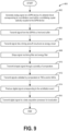
- FIG. 9 A method of operation of the readout circuit shown in FIG. 9 .
- Timing resolution may include optical transfer time spread, depth of interaction, wherein gamma rays of an annihilation event are detected in scintillator at different distances from photosensor(s), optical transfer efficiency, photodetection efficiency, single-photon time resolution (SPTR), crosstalk, dark counts (e.g., responses of photonic detectors in the absence of light), and readout electronics noise, bandwidth, and transient response.
- optical transfer time spread depth of interaction
- photodetection efficiency e.g., photodetection efficiency
- SPTR single-photon time resolution
- crosstalk e.g., responses of photonic detectors in the absence of light
- dark counts e.g., responses of photonic detectors in the absence of light
- readout electronics noise bandwidth, and transient response.
- Single-photon time resolution accounts for precision in determining time of arrival of a single scintillating photon at a photosensor.
- SPTR may significantly influence timing resolution.
- BGO scintillator crystals emit Cherenkov light as a result from gamma ray interactions. Cherenkov light is produced when a charged particle travels through matter faster than the speed of light. Photoelectrons may emit Cherenkov light for approximately 1-20 ps.
- Each SiPM device has an independent front-end readout circuit in the analog application-specific integrated circuit (ASIC).
- the front-end readout circuits of each SiPM device provide individual measurements of time stamps and signal amplitude or charges. Signals for timing and energy measurements are shaped by filters.
- a timing pick-off method implements multiple comparators for each signal to provide additional information about detected photons on the initial part of the scintillation pulses and corresponding rise time of each pulse, wherein the plurality of comparators are configured with a lowest timing pick-off threshold of 1/3 SPE, allowing for detection of Cherenkov photons. In this way, timing resolution in identification of events may be improved via detection of Cherenkov photons. Improvement in timing resolution for BGO based PET scanners may in turn result in increased image quality and sensitivity.
- the phrase "reconstructing an image” is not intended to exclude embodiments of the present invention in which data representing an image is generated but a viewable imaging is not. Therefore, as used herein, the term “image” broadly refers to both viewable images and data representing a viewable image. However, many embodiments generate, or are configured to generate, at least one viewable image.
- Multi-modality imaging system 10 may be any type of imaging system, for example, different types of medical imaging systems, such as a Positron Emission Tomography (PET), a Single Photon Emission Computed Tomography (SPECT), a Computed Tomography (CT), an ultrasound system, Magnetic Resonance Imaging (MRI), or any other system capable of generating tomographic images.
- PET Positron Emission Tomography
- SPECT Single Photon Emission Computed Tomography
- CT Computed Tomography
- MRI Magnetic Resonance Imaging
- the various embodiments are not limited to multi-modality medical imaging systems, but may be used on a single modality medical imaging system such as a stand-alone PET imaging system, for example.
- the various embodiments are not limited to medical imaging systems for imaging human subjects, but may include veterinary or non-medical systems for imaging non-human objects.
- the multi-modality imaging system 10 includes a first modality unit 11 and a second modality unit 12.
- the two modality units enable the multi-modality imaging system 10 to scan an object or patient in a second modality using the second modality unit 12.
- the multi-modality imaging system 10 allows for multiple scans in different modalities to facilitate an increased diagnostic capability over single modality systems.
- multi-modality imaging system 10 is a Computed Tomography/Positron Emission Tomography (CT/PET) imaging system 10, e.g., the first modality 11 is a CT imaging system 11 and the second modality 12 is a PET imaging system 12.
- CT/PET Computed Tomography/Positron Emission Tomography
- the first modality 11 is a CT imaging system 11
- the second modality 12 is a PET imaging system 12.
- the PET imaging system 12 may be a TOF PET system.
- the CT/PET system 10 is shown as including a gantry 13 representative of a CT imaging system and a gantry 14 that is associated with a PET imaging system. As discussed above, modalities other than CT and PET may be employed with the multi-modality imaging system 10.
- the gantry 13 includes an x-ray source 15 that projects a beam of x-rays toward a detector array 18 on the opposite side of the gantry 13.
- Detector array 18 is formed by a plurality of detector blocks (not shown) including a plurality of detector elements which together sense the projected x-rays that pass through a medical patient 22.
- Each detector element produces an electrical signal that represents the intensity of an impinging x-ray beam and hence allows estimation of the attenuation of the beam as it passes through the patient 22.
- gantry 13 and the components mounted thereon rotate about a center of rotation.
- FIG. 2 is a block schematic diagram of the PET imaging system 12 illustrated in FIG. 1 in accordance with an embodiment of the present invention.
- the PET imaging system 12 includes a detector ring assembly 40 including a plurality of detector blocks.
- the PET imaging system 12 also includes a controller or processor 44 to control normalization, image reconstruction processes and perform calibration. Controller 44 is coupled to an operator workstation 46. Controller 44 includes a data acquisition processor 48 and an image reconstruction processor 50, which are interconnected via a communication link 52.
- PET imaging system 12 acquires scan data and transmits the data to a data acquisition processor 48. The scanning operation is controlled from the operator workstation 46. The data acquired by the data acquisition processor 48 is reconstructed using the image reconstruction processor 50.
- the detector ring assembly 40 includes a central opening, in which an object or patient, such as patient 22 may be positioned using, for example, a motorized table 24 (shown in FIG. 1 ).
- the motorized table 24 is aligned with the central axis of detector ring assembly 40. This motorized table 24 moves the patient 22 into the central opening of detector ring assembly 40 in response to one or more commands received from the operator workstation 46.
- a PET scanner controller 54 also referred to as the PET gantry controller, is provided (e.g., mounted) within PET system 12.
- the PET scanner controller 54 responds to the commands received from the operator workstation 46 through the communication link 52. Therefore, the scanning operation is controlled from the operator workstation 46 through PET scanner controller 54.
- a photon e.g., a gamma ray
- a scintillation crystal 62 of a detector block 63 on a detector ring 40 When a photon (e.g., a gamma ray) collides with a scintillation crystal 62 of a detector block 63 on a detector ring 40, it produces a scintillation event on the crystal.
- Each photomultiplier tube or photosensor e.g., a SiPM device
- a set of acquisition circuits 66 e.g., readout circuits
- Acquisition circuits 66 produce digital signals indicating the three-dimensional (3D) location, total energy of the event, and the time or moment the scintillation event occurred. These digital signals are transmitted through a communication link, for example, a cable, to an event locator circuit 68 in the data acquisition processor 48.
- the data acquisition processor 48 includes the event locator circuit 68, an acquisition CPU 70, and a coincidence detector 72.
- the data acquisition processor 48 periodically samples the signals produced by the acquisition circuits 66.
- the acquisition CPU 70 controls communications on a back-plane bus 74 and on the communication link 52.
- the event locator circuit 68 processes the information regarding each valid event and provides a set of digital numbers or values indicative of the detected event. For example, this information indicates when the event took place and the position of the scintillation crystal 62 or detector block 63 that detected the event.
- An event data packet is communicated to the coincidence detector 72 through the back-plane bus 74.
- the coincidence detector 72 receives the event data packets from the event locator circuit 68 and determines if any two of the detected events are in coincidence.
- Coincidence is determined by a number of factors. First, the time markers in each event data packet must be within a predetermined time period, for example, 5 nanoseconds, of each other. Second, a LOR 35 formed by a straight line joining the two detectors that detect the coincidence event should pass through the field of view in the PET imaging system 12. Events that cannot be paired are discarded. Coincident event pairs are located and recorded as a coincidence data packet that is communicated through a physical communication link 78 to a sorter/histogrammer 80 in the image reconstruction processor 50.
- the image reconstruction processor 50 includes the sorter/histogrammer 80.
- sorter/histogrammer 80 generates a data structure known as a histogram.
- a histogram includes a large number of cells, where each cell corresponds to a unique pair of detector crystals in the PET scanner. Because a PET scanner typically includes thousands of detector crystals, the histogram typically includes millions of cells.
- Each cell of the histogram also stores a count value representing the number of coincidence events detected by the pair of detector crystals for that cell during the scan. At the end of the scan, the data in the histogram is used to reconstruct an image of the patient.
- histogram The completed histogram containing all the data from the scan is commonly referred to as a "result histogram.”
- the term “histogrammer” generally refers to the components of the scanner, e.g., processor and memory, which carry out the function of creating the histogram.
- the image reconstruction processor 50 also includes a memory module 82, an image CPU 84, an array processor 86, and a communication bus 88.
- the sorter/histogrammer 80 counts all events occurring along each projection ray and organizes the events into 3D data. This 3D data, or sinogram, is organized in one exemplary embodiment as a data array 90.
- Data array 90 is stored in the memory module 82.
- the communication bus 88 is linked to the communication link 52 through the image CPU 84.
- the image CPU 84 controls communication through communication bus 88.
- the array processor 86 is also connected to the communication bus 88.
- the array processor 86 receives data array 90 as an input and reconstructs images in the form of image array 92. Resulting image arrays 92 are then stored in memory module 82.
- the images stored in the image array 92 are communicated by the image CPU 84 to the operator workstation 46.
- the operator workstation 46 includes a CPU 94, a display 96, and an input device 98.
- the CPU 94 connects to communication link 52 and receives inputs, e.g., user commands, from the input device 98.
- the input device 98 may be, for example, a keyboard, mouse, a touch-screen panel, and/or a voice recognition system, and so on.
- the operator can control the operation of the PET imaging system 12 and the positioning of the patient 22 for a scan.
- the operator can control the display of the resulting image on the display 96 and can perform image-enhancement functions using programs executed by the workstation CPU 94.
- the detector ring assembly 40 includes a plurality of detector units (e.g., detector blocks).
- the detector unit may include a plurality of detectors (e.g., photosensors such as SiPM devices), light guides, scintillation crystals and ASICs, as will be further described in detail below.
- the detector unit may include twelve SiPM devices, four light guides, and two or more analog ASICs.
- the detector unit may include between 16 and 64 SiPM devices, no light guides, and one or more ASICs.
- the detector block 63 may include an array of scintillation crystals and an array of SiPM devices.
- the detector block 63 may be arranged with one-to-one coupling between scintillation crystals and SiPM devices, wherein each scintillation crystal is optically isolated from adjacent scintillation crystals via either a separating reflector or a light sharing reflector, as will be further described below.
- Each SiPM device may be read out by independent front-end readout circuits, via a timing pick-off channel and an energy channel. Signals from the timing pick-off channels and the energy channels may be sent ultimately to either Time-to-Digital converters (TDCs) or Analog-to-Digital converters (ADCs) after passing through one or more comparators.
- TDCs Time-to-Digital converters
- ADCs Analog-to-Digital converters
- the PET detector block 300 may be one of the plurality of detector units that comprise the detector ring assembly 40 of FIG. 2 , for example the PET detector block 300 may be the detector block 63.
- the PET detector block 300 may be configured with one-to-one coupling between scintillator crystals and SiPM devices.
- the PET detector block 300 comprises an array of scintillation crystals 302 and an array of SiPM devices 306.
- the scintillation crystals are BGO scintillation crystals.
- the array of scintillation crystals 302 comprises a plurality of crystals 304 and the array of SiPM devices 306 comprises a plurality of SiPM devices 308. In one example, there may be between 16 and 64 SiPM devices and scintillation crystals per detector block.
- Each of the plurality of crystals 304 is optically coupled to one of the plurality of SiPM devices 308, as is shown via coupling lines 310.
- each of the plurality of crystals 304 may be optically isolated from one another, as is depicted in FIG. 4 . In other examples, pairs of crystals share light while being optically isolated from other adjacent crystals, as is depicted in FIG. 5A .
- a first scintillation crystal 314 may be optically coupled to a first SiPM device 312 such that when one or more gamma rays collide with (e.g., are stopped within) the first scintillation crystal 314, the first SiPM device 312 detects the produced light from the first scintillation crystal 314 and sends signals to be read by a corresponding readout circuit.
- the PET detector block 300 may be surrounded by a reflective film (e.g., Teflon or other specular or diffusive material).
- the reflective film may be a light tight cover that does not allow emitted light from scintillation crystals to pass therethrough.
- each crystal of an array of scintillation crystals of a detector block as herein disclosed may be optically isolated from each other.
- FIG. 4 specifically depicts a schematic lateral view of a portion of a detector block 400, illustrating a row of scintillation crystals 402 within the array.
- Each scintillation crystal within the row of scintillation crystals 402 may be optically coupled to one SiPM device of a row of SiPM devices 408.
- the scintillation crystals herein described may be BGO scintillation crystals.
- Each SiPM device within the detector block 400 may have dimensions equal to dimensions of a corresponding scintillation crystal.
- a first scintillation crystal 404 may have a first width 450 and a first SiPM device 412 may have a second width 452.
- the first width 450 and the second width 452 may be equal to each other.
- an area of an end of the first scintillation crystal 404 may be equal to an area of an end of the first SiPM device 412.
- each of the SiPM devices may be configured for optical coupling to one of the crystals without overlap between.
- the detector block 400 may further comprise a plurality of separating reflectors 406.
- Each of the separating reflectors 406 may be positioned directly adjacent to one of the scintillation crystals 402.
- the plurality of separating reflectors 406 may be configured to optically isolate adjacent scintillation crystals from one another such that each scintillation crystal, in response to a photon being stopped therewithin, emits light to only one SiPM device.
- the first scintillation crystal 404 may be adjacent to a second scintillation crystal 414 and a third scintillation crystal 416.
- the first scintillation crystal 404 may be positioned between the second and third scintillation crystals 414, 416.
- a first separating reflector 418 may be positioned between the first scintillation crystal 404 and the second scintillation crystal 414 and a second separating reflector 420 may be positioned between the first scintillation crystal 404 and the third scintillation crystal 416.
- a gamma ray 410 e.g., a photon
- light is emitted, illustrated in FIG. 4 by arrows emitting from the gamma ray 410 within the first scintillation crystal 404.
- the first and second separating reflectors 418 and 420 may reflect the emitted light such that the light is not shared with the second and third scintillation crystals 414 and 416.
- the light may be sensed by the first SiPM device 412 and not with any adjacent SiPM devices. In this way, signals produced by the first SiPM device 412 may be known for gamma rays interacting with the first scintillation crystal 404.
- pairs of adjacent scintillation crystals may share light while being optically isolated from other scintillation crystals in an array of crystals.
- FIG. 5A specifically depicts a schematic lateral view of a portion of a detector block 500, illustrating a row of scintillation crystals 502 within the array.
- the row of scintillation crystals 502 may be partitioned into pairs of scintillation crystals, for example a first pair of crystals 550 may comprise a first crystal 510 and a second crystal 512
- the detector block 500 may further comprise a plurality of separating reflectors 504 and a plurality of light sharing reflectors 506, wherein each pair of crystals is optically isolated from adjacent pairs by one of the plurality of separating reflectors 504 and each of the plurality of light sharing reflectors 506 is positioned between crystals of a pair of crystals.
- Each of the plurality of light sharing reflectors 506 may be configured to allow emitted light to pass through and provide depth of interaction information/estimation to readout electronics in communication with SiPM devices.
- the first crystal 510 and the second crystal 512 of the first pair of crystals 550 may be separated by a light sharing reflector 514 such that light emitted by either the first or second crystal 510, 512 may be shared with the other of the first and second crystals 510, 512.
- the first crystal 510 may be adjacent to a third crystal 516 that is one of a second pair of crystals 552.
- the first crystal 510 may be optically separated from the third crystal 516 by a first separating reflector 520 such that light emitted by the first crystal 510 does not share with the third crystal 516.
- the second crystal 512 may be adjacent to a fourth crystal 518 that is one of a third pair of crystals 554.
- the second crystal 512 may be optically separated from the fourth crystal 518 by a second separating reflector 522.
- a gamma ray 560 interacts with the first crystal 510, light is emitted. Because the first pair of crystals 550 are able to share light via the light sharing reflector 514, emitted light may be shared with the second crystal 512 and thus light may be sensed by both a first SiPM device 524 that is optically coupled to the first crystal 510 and a second SiPM device 526 that is optically coupled to the second crystal 512.
- each SiPM device in either the first or second embodiment, may have individual front-end readout circuits and as such with two SiPM devices providing information to the front-end readout circuits, depth of interaction with regards to time of detection correction may be determined.
- method 900 includes transmitting the signal from the SiPM to a front-end buffer of an ASIC.
- Each SiPM of the detector block may be in communication with an individual front-end buffer and therefore a plurality of front-end buffers may be included in the ASIC.
- a technical effect of the systems and methods described herein is that Cherenkov photons may be detected with high timing resolution via the readout circuitry that includes a plurality of comparators and one or more filters and thus BGO scintillation crystals may be implemented into TOF PET systems.
- Thresholds for comparators within the circuitry may be set to 1/3 SPE with validation at 1.5-2.5 SPE, therefore suppressing dark counts while detecting emitted Cherenkov light for increased timing resolution.
- the array of scintillation crystals includes pairs of adjacent scintillation crystals that share light via light sharing reflectors and the pairs are optically isolated from one another via separating reflectors.
- information from the pairs of adjacent scintillation crystals provides depth of interaction estimation.
- the depth of interaction estimation is applied for timing measurement correction.
- the array of scintillation crystals is an array of bismuth germanate oxide (BGO) scintillation crystals, each BGO scintillation crystal configured to emit Cherenkov light, and each of the SiPM devices are configured to sense the Cherenkov light emitted by a corresponding scintillation crystal.
- BGO bismuth germanate oxide
- each independent front-end readout circuit comprises one or more Time-to-Digital converters (TDCs) and one or more analog to digital converters (ADCs) configured to digitize time-of-arrival, rise time, and energy signals from a corresponding SiPM device.
- TDCs Time-to-Digital converters
- ADCs analog to digital converters
- each independent front-end readout circuit is configured for dark count suppression at 1.5 SPE.
- the disclosure also provides support for a method for an imaging system, comprising: sensing light emitted by a scintillation crystal via a silicon photomultiplier (SiPM) device of a detector block in response to an annihilation event, transmitting an analog signal from the SiPM device to a front-end buffer of a readout circuit, shaping the analog signal with one or more filters of the readout circuit, comparing the analog signal to one or more thresholds via a plurality of comparators of the readout circuit, and digitizing the analog signal with one or more time to digital converters (TDCs) and one or more analog to digital converters (aDCs).
- the method further comprises: validating the analog signal to suppress dark counts.
- the SiPM device is one of a plurality of SiPM devices in an array, wherein each SiPM device in the array is readout by individual readout circuits.
- the analog signal comprises a timing signal and an energy signal, the timing signal shaped by a timing filter of the one or more filters and the energy signal shaped by an energy filter of the one or more filters.
- each of the array of scintillation crystals is a bismuth germanate oxide (BGO) scintillation crystal.
- each front-end readout circuit comprises a front-end buffer, a timing pick-off circuit, and an energy circuit, wherein the timing pick-off circuit comprises a plurality of comparators configured to estimate rise time within 1-5 nanoseconds of a pulse.
- the readout electronics are configured to be triggered at a first level of 1/3 single photoelectron (SPE) and validated at a second level of 1.5 SPE.
- SPE single photoelectron
Landscapes
- Health & Medical Sciences (AREA)
- Life Sciences & Earth Sciences (AREA)
- Physics & Mathematics (AREA)
- High Energy & Nuclear Physics (AREA)
- Molecular Biology (AREA)
- Spectroscopy & Molecular Physics (AREA)
- General Physics & Mathematics (AREA)
- Engineering & Computer Science (AREA)
- Medical Informatics (AREA)
- Microelectronics & Electronic Packaging (AREA)
- Heart & Thoracic Surgery (AREA)
- Public Health (AREA)
- Radiology & Medical Imaging (AREA)
- Pathology (AREA)
- Surgery (AREA)
- Animal Behavior & Ethology (AREA)
- General Health & Medical Sciences (AREA)
- Biomedical Technology (AREA)
- Veterinary Medicine (AREA)
- Optics & Photonics (AREA)
- Nuclear Medicine, Radiotherapy & Molecular Imaging (AREA)
- Biophysics (AREA)
- Nuclear Medicine (AREA)
- Measurement Of Radiation (AREA)
Applications Claiming Priority (1)
| Application Number | Priority Date | Filing Date | Title |
|---|---|---|---|
| US18/335,909 US20240418879A1 (en) | 2023-06-15 | 2023-06-15 | Systems and methods for time of flight positron emission tomography |
Publications (1)
| Publication Number | Publication Date |
|---|---|
| EP4478091A1 true EP4478091A1 (de) | 2024-12-18 |
Family
ID=91431474
Family Applications (1)
| Application Number | Title | Priority Date | Filing Date |
|---|---|---|---|
| EP24178407.3A Pending EP4478091A1 (de) | 2023-06-15 | 2024-05-28 | Systeme und verfahren zur flugzeitpositronenemissionstomographie |
Country Status (3)
| Country | Link |
|---|---|
| US (1) | US20240418879A1 (de) |
| EP (1) | EP4478091A1 (de) |
| CN (1) | CN119138912A (de) |
Citations (1)
| Publication number | Priority date | Publication date | Assignee | Title |
|---|---|---|---|---|
| US20210093261A1 (en) * | 2019-10-01 | 2021-04-01 | GE Precision Healthcare LLC | Methods and systems for pet detectors |
Family Cites Families (5)
| Publication number | Priority date | Publication date | Assignee | Title |
|---|---|---|---|---|
| US7173247B2 (en) * | 2003-09-24 | 2007-02-06 | Radiation Monitoring Devices, Inc. | Lu1-xI3:Cex—a scintillator for gamma ray spectroscopy and time-of-flight PET |
| US9405023B2 (en) * | 2013-02-12 | 2016-08-02 | General Electric Company | Method and apparatus for interfacing with an array of photodetectors |
| US10310098B1 (en) * | 2018-10-05 | 2019-06-04 | Canon Medical Systems Corporation | Determine position of scattered events in pixelated gamma detector using inverse energy weighting |
| CA3124832C (en) * | 2019-01-08 | 2024-03-05 | The Research Foundation For The State University Of New York | Prismatoid light guide |
| EP3859400B1 (de) * | 2020-01-31 | 2025-11-05 | Canon Medical Systems Corporation | Vorrichtung und verfahren zur strahlungsabbildung |
-
2023
- 2023-06-15 US US18/335,909 patent/US20240418879A1/en active Pending
-
2024
- 2024-05-28 EP EP24178407.3A patent/EP4478091A1/de active Pending
- 2024-06-13 CN CN202410760198.7A patent/CN119138912A/zh active Pending
Patent Citations (1)
| Publication number | Priority date | Publication date | Assignee | Title |
|---|---|---|---|---|
| US20210093261A1 (en) * | 2019-10-01 | 2021-04-01 | GE Precision Healthcare LLC | Methods and systems for pet detectors |
Non-Patent Citations (3)
| Title |
|---|
| FITZPATRICK TIM MAXIMILIAN: "A compton camera prototype with [gamma]-PET imaging capability: from component evaluations to online tests", 22 February 2022 (2022-02-22), pages 1 - 266, XP093095119, Retrieved from the Internet <URL:https://edoc.ub.uni-muenchen.de/29791/1/Fitzpatrick_Tim_Maximilian.pdf> [retrieved on 20231025] * |
| PARK HAEWOOK ET AL: "Silicon photomultiplier signal readout and multiplexing techniques for positron emission tomography: a review", BIOMEDICAL ENGINEERING LETTERS, THE KOREAN SOCIETY OF MEDICAL AND BIOLOGICAL ENGINEERING, KOREA, vol. 12, no. 3, 16 July 2022 (2022-07-16), pages 263 - 283, XP037909804, ISSN: 2093-9868, [retrieved on 20220716], DOI: 10.1007/S13534-022-00234-Y * |
| ZHAO ZHIXIANG ET AL: "An Advanced 100-Channel Readout System for Nuclear Imaging", IEEE TRANSACTIONS ON INSTRUMENTATION AND MEASUREMENT, IEEE, USA, vol. 68, no. 9, 1 September 2019 (2019-09-01), pages 3200 - 3210, XP011739240, ISSN: 0018-9456, [retrieved on 20190808], DOI: 10.1109/TIM.2018.2877952 * |
Also Published As
| Publication number | Publication date |
|---|---|
| CN119138912A (zh) | 2024-12-17 |
| US20240418879A1 (en) | 2024-12-19 |
Similar Documents
| Publication | Publication Date | Title |
|---|---|---|
| US8269177B2 (en) | Multiplexing readout scheme for a gamma ray detector | |
| JP5771197B2 (ja) | 定量化能力が改善されたpet検出器システム | |
| US6448559B1 (en) | Detector assembly for multi-modality scanners | |
| US9029786B2 (en) | Nuclear medicine imaging apparatus, and nuclear medicine imaging method | |
| US9069089B2 (en) | Methods and systems for increasing the sensitivity of simultaneous multi-isotope positron emission tomography | |
| US9575192B1 (en) | Optical channel reduction method and apparatus for photodetector arrays | |
| US7402807B2 (en) | Method for reducing an electronic time coincidence window in positron emission tomography | |
| US20120138804A1 (en) | Line of response estimation for high-resolution pet detector | |
| US20040227091A1 (en) | Methods and apparatus for radiation detecting and imaging using monolithic detectors | |
| US8969814B2 (en) | System and method of determining timing triggers for detecting gamma events for nuclear imaging | |
| US8481947B2 (en) | Method and system for nuclear imaging using multi-zone detector architecture | |
| JP2005533245A (ja) | 陽電子放射断層撮影(pet)用及び単一光子放射コンピュータ断層撮影(spect)用のガンマ線検出器 | |
| US9903961B1 (en) | Photodetector array readout multiplexer having summing, pulse shaping, and dynamic-switching circuits | |
| CN112587159B (zh) | 用于pet检测器的方法和系统 | |
| CN112470039B (zh) | 用于通过伽马辐射探测进行成像的系统和方法 | |
| CN108152849A (zh) | 放射线检测装置 | |
| US20130320218A1 (en) | Method and system for nuclear imaging using multi-zone detector architecture | |
| JP2006214916A (ja) | 放射線検査装置および放射線検査方法 | |
| JP2024091556A (ja) | 装置、およびタイムウォーク補正方法 | |
| US9612344B2 (en) | Positron emission tomography and single photon emission computed tomography based on intensity attenuation shadowing methods and effects | |
| US10088581B2 (en) | Method and a system for determining parameters of reactions of gamma quanta within scintillation detectors of PET scanners | |
| EP4478091A1 (de) | Systeme und verfahren zur flugzeitpositronenemissionstomographie | |
| Yamada et al. | Development of a small animal PET scanner using DOI detectors | |
| US6329657B1 (en) | Coincidence transmission source | |
| JP4997603B2 (ja) | 陽電子画像の感度を向上させる方法及び装置 |
Legal Events
| Date | Code | Title | Description |
|---|---|---|---|
| PUAI | Public reference made under article 153(3) epc to a published international application that has entered the european phase |
Free format text: ORIGINAL CODE: 0009012 |
|
| STAA | Information on the status of an ep patent application or granted ep patent |
Free format text: STATUS: REQUEST FOR EXAMINATION WAS MADE |
|
| 17P | Request for examination filed |
Effective date: 20240528 |
|
| AK | Designated contracting states |
Kind code of ref document: A1 Designated state(s): AL AT BE BG CH CY CZ DE DK EE ES FI FR GB GR HR HU IE IS IT LI LT LU LV MC ME MK MT NL NO PL PT RO RS SE SI SK SM TR |