EP4475175A2 - Übertragung von rfid-inlays von einem ersten substrat zu einem zweiten substrat - Google Patents
Übertragung von rfid-inlays von einem ersten substrat zu einem zweiten substrat Download PDFInfo
- Publication number
- EP4475175A2 EP4475175A2 EP24208702.1A EP24208702A EP4475175A2 EP 4475175 A2 EP4475175 A2 EP 4475175A2 EP 24208702 A EP24208702 A EP 24208702A EP 4475175 A2 EP4475175 A2 EP 4475175A2
- Authority
- EP
- European Patent Office
- Prior art keywords
- substrate
- rfid inlay
- adhesive
- rfid
- inlay
- Prior art date
- Legal status (The legal status is an assumption and is not a legal conclusion. Google has not performed a legal analysis and makes no representation as to the accuracy of the status listed.)
- Pending
Links
Images


Classifications
-
- G—PHYSICS
- G06—COMPUTING OR CALCULATING; COUNTING
- G06K—GRAPHICAL DATA READING; PRESENTATION OF DATA; RECORD CARRIERS; HANDLING RECORD CARRIERS
- G06K19/00—Record carriers for use with machines and with at least a part designed to carry digital markings
- G06K19/06—Record carriers for use with machines and with at least a part designed to carry digital markings characterised by the kind of the digital marking, e.g. shape, nature, code
- G06K19/067—Record carriers with conductive marks, printed circuits or semiconductor circuit elements, e.g. credit or identity cards also with resonating or responding marks without active components
- G06K19/07—Record carriers with conductive marks, printed circuits or semiconductor circuit elements, e.g. credit or identity cards also with resonating or responding marks without active components with integrated circuit chips
- G06K19/077—Constructional details, e.g. mounting of circuits in the carrier
- G06K19/07718—Constructional details, e.g. mounting of circuits in the carrier the record carrier being manufactured in a continuous process, e.g. using endless rolls
-
- G—PHYSICS
- G06—COMPUTING OR CALCULATING; COUNTING
- G06K—GRAPHICAL DATA READING; PRESENTATION OF DATA; RECORD CARRIERS; HANDLING RECORD CARRIERS
- G06K19/00—Record carriers for use with machines and with at least a part designed to carry digital markings
- G06K19/06—Record carriers for use with machines and with at least a part designed to carry digital markings characterised by the kind of the digital marking, e.g. shape, nature, code
- G06K19/067—Record carriers with conductive marks, printed circuits or semiconductor circuit elements, e.g. credit or identity cards also with resonating or responding marks without active components
- G06K19/07—Record carriers with conductive marks, printed circuits or semiconductor circuit elements, e.g. credit or identity cards also with resonating or responding marks without active components with integrated circuit chips
- G06K19/077—Constructional details, e.g. mounting of circuits in the carrier
- G06K19/07749—Constructional details, e.g. mounting of circuits in the carrier the record carrier being capable of non-contact communication, e.g. constructional details of the antenna of a non-contact smart card
-
- H—ELECTRICITY
- H10—SEMICONDUCTOR DEVICES; ELECTRIC SOLID-STATE DEVICES NOT OTHERWISE PROVIDED FOR
- H10P—GENERIC PROCESSES OR APPARATUS FOR THE MANUFACTURE OR TREATMENT OF DEVICES COVERED BY CLASS H10
- H10P72/00—Handling or holding of wafers, substrates or devices during manufacture or treatment thereof
- H10P72/70—Handling or holding of wafers, substrates or devices during manufacture or treatment thereof for supporting or gripping
- H10P72/74—Handling or holding of wafers, substrates or devices during manufacture or treatment thereof for supporting or gripping using temporarily an auxiliary support
-
- H—ELECTRICITY
- H10—SEMICONDUCTOR DEVICES; ELECTRIC SOLID-STATE DEVICES NOT OTHERWISE PROVIDED FOR
- H10P—GENERIC PROCESSES OR APPARATUS FOR THE MANUFACTURE OR TREATMENT OF DEVICES COVERED BY CLASS H10
- H10P72/00—Handling or holding of wafers, substrates or devices during manufacture or treatment thereof
- H10P72/70—Handling or holding of wafers, substrates or devices during manufacture or treatment thereof for supporting or gripping
- H10P72/74—Handling or holding of wafers, substrates or devices during manufacture or treatment thereof for supporting or gripping using temporarily an auxiliary support
- H10P72/7432—Handling or holding of wafers, substrates or devices during manufacture or treatment thereof for supporting or gripping using temporarily an auxiliary support used in a transfer process involving transfer directly from an origin substrate to a target substrate without use of an intermediate handle substrate
-
- H—ELECTRICITY
- H10—SEMICONDUCTOR DEVICES; ELECTRIC SOLID-STATE DEVICES NOT OTHERWISE PROVIDED FOR
- H10P—GENERIC PROCESSES OR APPARATUS FOR THE MANUFACTURE OR TREATMENT OF DEVICES COVERED BY CLASS H10
- H10P72/00—Handling or holding of wafers, substrates or devices during manufacture or treatment thereof
- H10P72/70—Handling or holding of wafers, substrates or devices during manufacture or treatment thereof for supporting or gripping
- H10P72/74—Handling or holding of wafers, substrates or devices during manufacture or treatment thereof for supporting or gripping using temporarily an auxiliary support
- H10P72/744—Details of chemical or physical process used for separating the auxiliary support from a device or a wafer
-
- H—ELECTRICITY
- H10—SEMICONDUCTOR DEVICES; ELECTRIC SOLID-STATE DEVICES NOT OTHERWISE PROVIDED FOR
- H10W—GENERIC PACKAGES, INTERCONNECTIONS, CONNECTORS OR OTHER CONSTRUCTIONAL DETAILS OF DEVICES COVERED BY CLASS H10
- H10W72/00—Interconnections or connectors in packages
- H10W72/01—Manufacture or treatment
- H10W72/0198—Manufacture or treatment batch processes
-
- H—ELECTRICITY
- H10—SEMICONDUCTOR DEVICES; ELECTRIC SOLID-STATE DEVICES NOT OTHERWISE PROVIDED FOR
- H10W—GENERIC PACKAGES, INTERCONNECTIONS, CONNECTORS OR OTHER CONSTRUCTIONAL DETAILS OF DEVICES COVERED BY CLASS H10
- H10W72/00—Interconnections or connectors in packages
- H10W72/071—Connecting or disconnecting
- H10W72/073—Connecting or disconnecting of die-attach connectors
-
- H—ELECTRICITY
- H10—SEMICONDUCTOR DEVICES; ELECTRIC SOLID-STATE DEVICES NOT OTHERWISE PROVIDED FOR
- H10W—GENERIC PACKAGES, INTERCONNECTIONS, CONNECTORS OR OTHER CONSTRUCTIONAL DETAILS OF DEVICES COVERED BY CLASS H10
- H10W72/00—Interconnections or connectors in packages
- H10W72/071—Connecting or disconnecting
- H10W72/073—Connecting or disconnecting of die-attach connectors
- H10W72/07302—Connecting or disconnecting of die-attach connectors using an auxiliary member
- H10W72/07304—Connecting or disconnecting of die-attach connectors using an auxiliary member the auxiliary member being temporary, e.g. a sacrificial coating
- H10W72/07307—Connecting or disconnecting of die-attach connectors using an auxiliary member the auxiliary member being temporary, e.g. a sacrificial coating the auxiliary member being a temporary substrate, e.g. a removable substrate
-
- H—ELECTRICITY
- H10—SEMICONDUCTOR DEVICES; ELECTRIC SOLID-STATE DEVICES NOT OTHERWISE PROVIDED FOR
- H10W—GENERIC PACKAGES, INTERCONNECTIONS, CONNECTORS OR OTHER CONSTRUCTIONAL DETAILS OF DEVICES COVERED BY CLASS H10
- H10W72/00—Interconnections or connectors in packages
- H10W72/071—Connecting or disconnecting
- H10W72/073—Connecting or disconnecting of die-attach connectors
- H10W72/07331—Connecting techniques
- H10W72/07337—Connecting techniques using a polymer adhesive, e.g. an adhesive based on silicone or epoxy
- H10W72/07338—Connecting techniques using a polymer adhesive, e.g. an adhesive based on silicone or epoxy hardening the adhesive by curing, e.g. thermosetting
-
- H—ELECTRICITY
- H10—SEMICONDUCTOR DEVICES; ELECTRIC SOLID-STATE DEVICES NOT OTHERWISE PROVIDED FOR
- H10W—GENERIC PACKAGES, INTERCONNECTIONS, CONNECTORS OR OTHER CONSTRUCTIONAL DETAILS OF DEVICES COVERED BY CLASS H10
- H10W72/00—Interconnections or connectors in packages
- H10W72/071—Connecting or disconnecting
- H10W72/073—Connecting or disconnecting of die-attach connectors
- H10W72/07351—Connecting or disconnecting of die-attach connectors characterised by changes in properties of the die-attach connectors during connecting
- H10W72/07354—Connecting or disconnecting of die-attach connectors characterised by changes in properties of the die-attach connectors during connecting changes in dispositions
-
- H—ELECTRICITY
- H10—SEMICONDUCTOR DEVICES; ELECTRIC SOLID-STATE DEVICES NOT OTHERWISE PROVIDED FOR
- H10W—GENERIC PACKAGES, INTERCONNECTIONS, CONNECTORS OR OTHER CONSTRUCTIONAL DETAILS OF DEVICES COVERED BY CLASS H10
- H10W72/00—Interconnections or connectors in packages
- H10W72/30—Die-attach connectors
- H10W72/321—Structures or relative sizes of die-attach connectors
- H10W72/325—Die-attach connectors having a filler embedded in a matrix
-
- H—ELECTRICITY
- H10—SEMICONDUCTOR DEVICES; ELECTRIC SOLID-STATE DEVICES NOT OTHERWISE PROVIDED FOR
- H10W—GENERIC PACKAGES, INTERCONNECTIONS, CONNECTORS OR OTHER CONSTRUCTIONAL DETAILS OF DEVICES COVERED BY CLASS H10
- H10W72/00—Interconnections or connectors in packages
- H10W72/30—Die-attach connectors
- H10W72/341—Dispositions of die-attach connectors, e.g. layouts
- H10W72/347—Dispositions of multiple die-attach connectors
-
- H—ELECTRICITY
- H10—SEMICONDUCTOR DEVICES; ELECTRIC SOLID-STATE DEVICES NOT OTHERWISE PROVIDED FOR
- H10W—GENERIC PACKAGES, INTERCONNECTIONS, CONNECTORS OR OTHER CONSTRUCTIONAL DETAILS OF DEVICES COVERED BY CLASS H10
- H10W72/00—Interconnections or connectors in packages
- H10W72/30—Die-attach connectors
- H10W72/351—Materials of die-attach connectors
- H10W72/352—Materials of die-attach connectors comprising metals or metalloids, e.g. solders
-
- H—ELECTRICITY
- H10—SEMICONDUCTOR DEVICES; ELECTRIC SOLID-STATE DEVICES NOT OTHERWISE PROVIDED FOR
- H10W—GENERIC PACKAGES, INTERCONNECTIONS, CONNECTORS OR OTHER CONSTRUCTIONAL DETAILS OF DEVICES COVERED BY CLASS H10
- H10W72/00—Interconnections or connectors in packages
- H10W72/30—Die-attach connectors
- H10W72/351—Materials of die-attach connectors
- H10W72/353—Materials of die-attach connectors not comprising solid metals or solid metalloids, e.g. ceramics
- H10W72/354—Materials of die-attach connectors not comprising solid metals or solid metalloids, e.g. ceramics comprising polymers
-
- H—ELECTRICITY
- H10—SEMICONDUCTOR DEVICES; ELECTRIC SOLID-STATE DEVICES NOT OTHERWISE PROVIDED FOR
- H10W—GENERIC PACKAGES, INTERCONNECTIONS, CONNECTORS OR OTHER CONSTRUCTIONAL DETAILS OF DEVICES COVERED BY CLASS H10
- H10W90/00—Package configurations
- H10W90/701—Package configurations characterised by the relative positions of pads or connectors relative to package parts
- H10W90/731—Package configurations characterised by the relative positions of pads or connectors relative to package parts of die-attach connectors
- H10W90/734—Package configurations characterised by the relative positions of pads or connectors relative to package parts of die-attach connectors between a chip and a stacked insulating package substrate, interposer or RDL
-
- H—ELECTRICITY
- H10—SEMICONDUCTOR DEVICES; ELECTRIC SOLID-STATE DEVICES NOT OTHERWISE PROVIDED FOR
- H10W—GENERIC PACKAGES, INTERCONNECTIONS, CONNECTORS OR OTHER CONSTRUCTIONAL DETAILS OF DEVICES COVERED BY CLASS H10
- H10W90/00—Package configurations
- H10W90/701—Package configurations characterised by the relative positions of pads or connectors relative to package parts
- H10W90/731—Package configurations characterised by the relative positions of pads or connectors relative to package parts of die-attach connectors
- H10W90/736—Package configurations characterised by the relative positions of pads or connectors relative to package parts of die-attach connectors between a chip and a stacked lead frame, conducting package substrate or heat sink
-
- H—ELECTRICITY
- H10—SEMICONDUCTOR DEVICES; ELECTRIC SOLID-STATE DEVICES NOT OTHERWISE PROVIDED FOR
- H10W—GENERIC PACKAGES, INTERCONNECTIONS, CONNECTORS OR OTHER CONSTRUCTIONAL DETAILS OF DEVICES COVERED BY CLASS H10
- H10W99/00—Subject matter not provided for in other groups of this subclass
Definitions
- the present subject matter relates to radio frequency identification (“RFID”) devices. More particularly, the present subject matter relates to systems and methods for transferring RFID inlays from one substrate to another.
- RFID radio frequency identification
- RFID tags and labels are widely used to associate an object with an identification code.
- RFID devices generally include an antennae and analog and/or digital electronics, which may include, for example, communications electronics, data memory, and control logic.
- RFID devices can be used for a variety of applications, for example, security locks in cars, access control to buildings, and tracking inventory and parcels.
- RFID devices One difficulty associated with RFID devices is securing the functional components (namely, an RFID chip and associated antenna) or "RFID inlay" to certain materials, such as ultra-soft fabric or very thin materials or exotic/unconventional materials, using conventional techniques. Providing an approach to securing an RFID inlay to such materials would be advantageous, particularly if such an approach also allowed for reduced manufacturing costs and promoted sustainability (i.e., reuse of selected materials used during the manufacturing process).
- the RFID inlay contains a chip electrically coupled to an antenna.
- the chip can be electrically coupled to an antenna using techniques known in the art.
- the chip is electrically conducted to an antenna using a conductive adhesive.
- the chip can be attached using a "direct-attach" process or a "strap attach" process.
- the antenna can be formed of materials known in the art.
- the antenna is formed from a metal or metallic material, such as aluminum, copper, or nickel.
- the metallic material is a metallic foil.
- the antenna is formed using a conducting ink.
- the method includes securing an RFID inlay to a first substrate.
- the first substrate is a conventional material, for example, polymeric (e.g., PET) materials, cellulose-based materials (e.g., paper), textiles, fabrics, knits, etc.
- the inlay can be secured using techniques known in the art.
- the inlay is secured to the substrate using an adhesive.
- the adhesive is applied in any desired pattern or configuration.
- the adhesive is applied in a shape or pattern that is desired for an antenna.
- the first adhesive is a conductive adhesive.
- the RFID inlay is then brought into the vicinity of a second substrate and secured to the second substrate with a second adhesive.
- the second substrate is a conventional substrate as described above.
- the second substrate is an unconventional material, for example, an ultra-soft fabric or very thin material or exotic material.
- the RFID inlay is then dissociated from the first substrate.
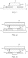
- Fig. 1 illustrates an exemplary RFID inlay 10 according to the present disclosure.
- the RFID inlay 10 of Fig. 1 includes an RFID chip 12 (which may be variously configured without departing from the scope of the present disclosure) that is electrically coupled to an antenna 14 (which also may be variously configured without departing from the scope of the present disclosure).
- the RFID chip 12 is coupled to the antenna 14 by a conductive adhesive 16, but different means for coupling the RFID chip 12 to the antenna 14 may be employed without departing from the scope of the present disclosure.
- the RFID inlay 10 is secured to a conventional substrate 18 (e.g., formed of a paper or polyethylene terephthalate material) by an adhesive 20.
- a conventional substrate 18 e.g., formed of a paper or polyethylene terephthalate material
- the manner in which the RFID inlay 10 is assembled and secured to the substrate 18 may vary without departing from the scope of the present disclosure.
- the substrate 18 is provided as a web of material that is unwound from a reel.
- the adhesive 20 is applied to the substrate 18 as the substrate 18 is unwound from the reel or, alternatively, if the adhesive 20 is already present on the substrate 18, a liner is removed to expose the adhesive 20 as the substrate 18 is unwound from the reel.
- the adhesive 20 is applied in the shape that is desired for an antenna 14 of the RFID inlay 10, but the adhesive 20 may be otherwise applied or configured without departing from the scope of the present disclosure.
- the substrate 18 with exposed adhesive 20 continues unwinding from the reel, with a conductive material being applied to at least portions of the adhesive 20.
- the conductive material may be applied according to any suitable approach and in any pattern without departing from the scope of the present disclosure, but according to one exemplary embodiment, a web of conductive material (e.g., an aluminum foil) is provided, with the conductive material being unwound from a reel and brought into contact with the adhesive 20.
- the conductive material (if not provided in a final configuration) is formed into the shape of an antenna (e.g., using a die- or laser-cutting procedure) and then any excess material is removed by any suitable approach.
- the adhesive 20 is provided in the shape that is desired for the antenna 24, in which case the conductive material may be stripped away from the substrate 18, which leaves only the portions of the conductive material in contact with the patterned adhesive 20, as an antenna 14.
- the substrate 18 (with the conductive material in the shape of an antenna 14) is then wound onto a second reel.
- a plurality of antennas 14 may be sequentially applied to the substrate 18, allowing for the efficient creation of a plurality of RFID inlays 10.
- the substrate 18 (with the plurality of antennas 14) is subsequently unwound from the reel and a chip adhesive 16 is sequentially applied to each antenna 14.
- An RFID chip 12 is then applied to the chip adhesive 16 (using a "direct chip attach” approach or a "strap attach” approach, for example) to electrically couple the RFID chip 12 to an associated antenna 14. This may include applying pressure and/or heat to cure the chip adhesive 16 and bond the RFID chip 12 to the antenna 14, thereby forming an RFID inlay 10.
- each RFID inlay 10 may be tested, with the substrate 18 (with the plurality of RFID inlays 10) being wound onto another reel.
- a second substrate 22 is secured to the RFID inlay using a second adhesive 24, as in Fig. 2 .
- the first substrate 18 is formed of a conventional substrate material.
- the second substrate 22 may also be formed of a conventional substrate material, it may instead be formed of an unconventional material (e.g., an ultra-soft fabric or very thin material or exotic material) that is not well-suited for conventional approaches to applying an RFID inlay to a substrate (e.g., the above-described approach to applying the RFID inlay 10 to the first substrate 18).
- the first substrate 18 is dissociated from the RFID inlay 10, leaving the RFID inlay 10 secured only to the second substrate 22, as in Fig. 3 .
- an additional or third substrate e.g., a liner
- the first substrate 18 may be dissociated from the RFID inlay 10 using any one of a variety of different approaches and systems, with exemplary approaches and systems to be described herein in greater detail.
- an additional layer 26 (e.g., a thermal transfer adhesive layer) is provided between the first substrate 18 and the first adhesive 20 ( Fig. 4 ).
- the assembly of Fig. 4 may be manufactured according to any suitable approach, including an approach of the type described above. If the above-described approach were employed, an additional step of applying the additional layer 26 to the first substrate 18 is provided before the first adhesive 20 is applied, with the first adhesive 20 being applied to the additional layer 26, rather than being applied directly to the first substrate 18.
- a second substrate 22 may be secured to the RFID inlay 10 according to any suitable approach (including the above-described approach), resulting in the assembly of Fig. 5 .
- the RFID inlay 10 is dissociated from the first substrate 18 using a method and/or system according to the present disclosure, resulting in the assembly of Fig. 3 .
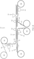
- Figs. 6 and 7 illustrate exemplary systems 28 and 30 for transferring an RFID inlay 10 from a first substrate 18 to a second substrate 22. It should be understood that the illustrated systems 28 and 30 and the associated transfer methods are merely exemplary and that differently configured systems and methods may be employed without departing from the scope of the present disclosure.
- a first substrate 18 having a plurality of RFID inlays 10 secured thereto is provided on a reel 32.
- the second substrate 22 is also provided on a reel 34. Both of the substrates 18 and 22 are unwound from their respective reels 32 and 34 by any suitable mechanism (e.g., rollers 36 in the illustrated embodiment). If the second substrate 22 is provided with a layer of adhesive 24 and a liner 38, the liner 38 may be unwound from the second substrate 22 onto a reel 40 to expose the adhesive 24. On the other hand, if the second substrate 22 does not include adhesive, an adhesive applicator 42 may be provided to apply adhesive 24 (e.g., in the form of a spray) to the second substrate 22 as the second substrate 22 is unwound from the reel 34.
- adhesive 24 e.g., in the form of a spray
- the RFID inlay 10 is brought into the vicinity of the second substrate 22, with the adhesive 24 on the second substrate 22 facing the RFID inlay 10 on the first substrate 18.
- the RFID inlay 10 is secured to the second substrate 22 using the adhesive 24 on the second substrate 22. This results in the configuration shown in Figs. 2 or 4 , for example, with the RFID chip 12 in contact with the adhesive 24 on the second substrate 22, while the antenna 14 is in contact with the adhesive 20 on the first substrate 18.
- the RFID inlay 10 is next dissociated from the first substrate 18. This may include first softening the adhesive 20 on the first substrate 18 before dissociating the RFID inlay 10 and the first substrate 18 or instead dissociating the RFID inlay 10 from the first substrate 18 without first softening the adhesive 20 on the first substrate 22.
- the adhesive 20 on the first substrate 18 may be softened by any of a number of possible approaches, which depend upon the nature of the adhesive 20. In one embodiment, heat is applied to soften the adhesive 20 on the first substrate 18 (as indicated at 46 in Fig. 6 ). In another embodiment, a softening substance or agent (e.g., a solvent) is applied to soften the adhesive 20 on the first substrate 18.
- the two substrates 18 and 22 are moved apart from each other (e.g., by directing the first substrate 18 in a direction away from the second substrate 22, as in Fig. 6 ). Moving the substrates 18 and 22 away from each other results in application of a release force that overcomes the release strength of the softened adhesive 20 on the first substrate 18 (thereby dissociating the RFID inlay 10 from the first substrate 18) without dissociating the RFID inlay 10 from the second substrate 22.
- This results in the configuration shown in Fig. 3 for example, with the RFID inlay 10 secured only to the second substrate 22.
- the adhesive 20 on the first substrate 18 is not first softened before dissociating the RFID inlay 10 from the first substrate 18, then care must be taken in selecting appropriate adhesives 20 and 24.
- the adhesive 20 on the first substrate 18 is not first softened, its release strength should be less than the release strength of the adhesive 24 on the second substrate 22.
- the first substrate 10 may be wound onto a second reel 48 for reuse (e.g., for receiving additional RFID inlays and then transferring additional RFID inlays to a different substrate, as described herein). Reusing the first substrate 18 rather than disposing of it promotes sustainability while also reducing the costs for manufacturing the RFID devices into which the RFID inlays 10 are incorporated (by reducing the material costs).
- a third substrate 50 (which may be a liner or back face provided as a web of material) is secured to the RFID inlay 10 (e.g., using an adhesive), with the RFID inlay 10 positioned between the second substrate 22 and the third substrate 50.
- Fig. 6 also shows (at position 52) the second substrate 22 being cut between adjacent RFID inlays 10 (e.g., by die-cutting or laser-cutting) to define individual RFID tags or labels.
- the individual RFID tags or labels may be tested (e.g., as indicated at 54 in Fig.
- the third substrate 50 being wound onto a finished product reel 56, with the individual RFID tags or labels being ready for removal from the third substrate 50 and attachment to or incorporation into an article or piece of merchandise.
- the third substrate 50 is also cut between adjacent RFID inlays 10 to define separate RFID tags or labels, the separate RFID tags or labels may be collected for subsequent attachment to or incorporation into an article or piece of merchandise.
- Fig. 7 shows another exemplary system 30 (which may be described as having a "super tight pitch” configuration) that may be employed to transfer an RFID inlay 10 from a first substrate 18 to a second substrate 22. Similar to the system 28 of Fig. 6 , Fig. 7 shows a system 30 in which both the first substrate 18 and the second substrate 22 are provided on reels 58 and 60, respectively. Both of the substrates 18 and 22 are unwound from their respective reels 58 and 60 by any suitable mechanism (e.g., rollers 62 in the illustrated embodiment). In the illustrated embodiment, the second substrate 22 is provided with a layer of adhesive 24 and a liner 64, with the liner 64 being unwound from the second substrate 22 to expose the adhesive 24.
- the liner 64 is not immediately wound onto a second reel, but rather is directed along a path that departs from the second substrate 22 (with the first substrate 18 being directed along a path positioned between the diverging paths of the second substrate 18 and the liner 64) before being brought back into the vicinity of the second substrate 22 for attachment to the RFID inlays 10, as will be described in greater detail herein.
- the RFID inlays 10 are brought into the vicinity of the second substrate 22, with the adhesive 24 on the second substrate 22 facing the RFID inlays 10 on the first substrate 18.
- the RFID inlay 10 is secured to the second substrate 22 using the adhesive 24 on the second substrate 22.
- Fig. 7 shows a tamp 68 being employed to move the first substrate 18 toward the second substrate 22, but other approaches may be employed without departing from the scope of the present disclosure.
- Securing an RFID inlay 10 to the second substrate 22 results in the configuration shown in Figs. 2 or 4 , for example, with the RFID chip 12 in contact with the adhesive 24 on the second substrate 22, while the antenna 14 is in contact with the adhesive 20 on the first substrate 18.
- the RFID inlay 10 is next dissociated from the first substrate 18. This may include first softening the adhesive 20 on the first substrate 18 before dissociating the RFID inlay 10 and the first substrate 18 or instead dissociating the RFID inlay 10 from the first substrate 18 without first softening the adhesive 20 on the first substrate 18, as described above in greater detail with regard to the system 28 of Fig. 6 . Regardless of the particular approach employed to dissociate the RFID inlay 10 from the first substrate 18, the result is the configuration shown in Fig. 3 , for example, with the RFID inlay 10 secured only to the second substrate 22. After the RFID inlay 10 has been dissociated from the first substrate 18, the first substrate 18 may be wound onto a second reel 70 for reuse, thus promoting sustainability and reducing manufacturing costs.
- the assembly may be subjected to further processing.
- the liner 64 initially separated from the second substrate 22 is redirected back into the vicinity of the second substrate 22 and secured to the RFID inlay (e.g., using an adhesive that may be applied to the liner 64 between the time that the liner 6 is dissociated from the second substrate 22 and then brought back into the vicinity of the second substrate 22), with the RFID inlay 10 positioned between the second substrate 22 and the liner 64.
- Fig. 7 also shows (at position 72) the second substrate 22 being cut between adjacent RFID inlays 10 (e.g., by die-cutting or laser-cutting) to define individual RFID tags or labels.
- the individual RFID tags or labels may be tested (e.g., as indicated at 74 in Fig. 7 ), followed by the liner 64 being wound onto a finished product reel 76, with the individual RFID tags or labels being ready for removal from the liner 64 and attachment to or incorporation into an article or piece of merchandise.
- the liner 64 is also cut between adjacent RFID inlays 10 to define separate RFID tags or labels, the separate RFID tags or labels may be collected for subsequent attachment to or incorporation into an article or piece of merchandise.
- the post-dissociation processing steps described above and shown in Fig. 7 are merely exemplary and that other and/or additional processing steps may be employed without departing from the scope of the present disclosure.
Landscapes
- Engineering & Computer Science (AREA)
- Computer Hardware Design (AREA)
- Microelectronics & Electronic Packaging (AREA)
- Physics & Mathematics (AREA)
- General Physics & Mathematics (AREA)
- Theoretical Computer Science (AREA)
- Details Of Aerials (AREA)
- Credit Cards Or The Like (AREA)
- Adhesive Tapes (AREA)
Applications Claiming Priority (3)
| Application Number | Priority Date | Filing Date | Title |
|---|---|---|---|
| US202062975398P | 2020-02-12 | 2020-02-12 | |
| PCT/US2021/017650 WO2021163318A1 (en) | 2020-02-12 | 2021-02-11 | Transfer of rfid inlays from a first substrate to a second substrate |
| EP21710711.9A EP4104101B1 (de) | 2020-02-12 | 2021-02-11 | Übertragung von rfid-inlays von einem ersten substrat zu einem zweiten substrat |
Related Parent Applications (1)
| Application Number | Title | Priority Date | Filing Date |
|---|---|---|---|
| EP21710711.9A Division EP4104101B1 (de) | 2020-02-12 | 2021-02-11 | Übertragung von rfid-inlays von einem ersten substrat zu einem zweiten substrat |
Publications (2)
| Publication Number | Publication Date |
|---|---|
| EP4475175A2 true EP4475175A2 (de) | 2024-12-11 |
| EP4475175A3 EP4475175A3 (de) | 2025-02-26 |
Family
ID=74860453
Family Applications (2)
| Application Number | Title | Priority Date | Filing Date |
|---|---|---|---|
| EP21710711.9A Active EP4104101B1 (de) | 2020-02-12 | 2021-02-11 | Übertragung von rfid-inlays von einem ersten substrat zu einem zweiten substrat |
| EP24208702.1A Pending EP4475175A3 (de) | 2020-02-12 | 2021-02-11 | Übertragung von rfid-inlays von einem ersten substrat zu einem zweiten substrat |
Family Applications Before (1)
| Application Number | Title | Priority Date | Filing Date |
|---|---|---|---|
| EP21710711.9A Active EP4104101B1 (de) | 2020-02-12 | 2021-02-11 | Übertragung von rfid-inlays von einem ersten substrat zu einem zweiten substrat |
Country Status (5)
| Country | Link |
|---|---|
| US (1) | US11995493B2 (de) |
| EP (2) | EP4104101B1 (de) |
| JP (1) | JP7478500B2 (de) |
| CN (1) | CN115315707A (de) |
| WO (1) | WO2021163318A1 (de) |
Families Citing this family (1)
| Publication number | Priority date | Publication date | Assignee | Title |
|---|---|---|---|---|
| WO2025163552A1 (en) * | 2024-02-01 | 2025-08-07 | Avery Dennison Retail Information Services Llc | Wet strap attach process |
Family Cites Families (22)
| Publication number | Priority date | Publication date | Assignee | Title |
|---|---|---|---|---|
| US6147662A (en) * | 1999-09-10 | 2000-11-14 | Moore North America, Inc. | Radio frequency identification tags and labels |
| US6937153B2 (en) | 2002-06-28 | 2005-08-30 | Appleton Papers Inc. | Thermal imaging paper laminate |
| US7023347B2 (en) * | 2002-08-02 | 2006-04-04 | Symbol Technologies, Inc. | Method and system for forming a die frame and for transferring dies therewith |
| US6867983B2 (en) * | 2002-08-07 | 2005-03-15 | Avery Dennison Corporation | Radio frequency identification device and method |
| GB2395462B (en) | 2002-11-21 | 2006-04-05 | Hewlett Packard Co | Apparatus for printing and memory tag application and method therefor |
| US7930815B2 (en) * | 2003-04-11 | 2011-04-26 | Avery Dennison Corporation | Conductive pattern and method of making |
| US7244326B2 (en) * | 2003-05-16 | 2007-07-17 | Alien Technology Corporation | Transfer assembly for manufacturing electronic devices |
| JP4535700B2 (ja) * | 2003-07-25 | 2010-09-01 | トッパン・フォームズ株式会社 | Icラベル製造装置 |
| US7119685B2 (en) | 2004-02-23 | 2006-10-10 | Checkpoint Systems, Inc. | Method for aligning capacitor plates in a security tag and a capacitor formed thereby |
| WO2006016559A1 (ja) | 2004-08-09 | 2006-02-16 | Suncall Corporation | Icタグ付きシール及びその取り付け方法 |
| US7170415B2 (en) | 2004-12-01 | 2007-01-30 | Avery Dennison Corporation | RFID tags with modifiable operating parameters |
| US7576656B2 (en) * | 2005-09-15 | 2009-08-18 | Alien Technology Corporation | Apparatuses and methods for high speed bonding |
| US7828217B2 (en) * | 2006-03-27 | 2010-11-09 | Muhlbauer Ag | Method and device for producing RFID smart labels or smart label inlays |
| US7646304B2 (en) * | 2006-04-10 | 2010-01-12 | Checkpoint Systems, Inc. | Transfer tape strap process |
| JP2008204139A (ja) * | 2007-02-20 | 2008-09-04 | Toppan Forms Co Ltd | 非接触型データ受送信体 |
| JP2009086968A (ja) * | 2007-09-28 | 2009-04-23 | Dainippon Printing Co Ltd | Icタグ |
| JP5199010B2 (ja) | 2008-10-01 | 2013-05-15 | 富士通株式会社 | Rfidタグの製造方法およびrfidタグ |
| JP2010092143A (ja) * | 2008-10-06 | 2010-04-22 | Echigo Fudagami Kk | Icシート製造方法及びicシート製造装置 |
| US10807757B2 (en) * | 2013-04-26 | 2020-10-20 | Avery Dennison Corporation | Method and apparatus for dispensing pressure sensitive adhesive labels onto a substrate |
| BR112020009180B1 (pt) * | 2017-11-10 | 2022-12-20 | Avery Dennison Retail Information Services, Llc | Conjunto de pilha de etiquetas, configuração de cilindro de base para produzir referido conjunto e método |
| JP6941068B2 (ja) | 2018-02-21 | 2021-09-29 | サトーホールディングス株式会社 | アンテナパターンの製造方法、rfidインレイの製造方法、rfidラベルの製造方法及びrfid媒体の製造方法 |
| EP3772419B1 (de) * | 2019-08-08 | 2021-12-01 | HID Global GmbH | Verfahren zur herstellung einer bahnförmigen monolithischen folie mit integrierten sicherheitsmerkmalen und herstellungsmaschine |
-
2021
- 2021-02-11 EP EP21710711.9A patent/EP4104101B1/de active Active
- 2021-02-11 CN CN202180024351.4A patent/CN115315707A/zh active Pending
- 2021-02-11 JP JP2022549188A patent/JP7478500B2/ja active Active
- 2021-02-11 WO PCT/US2021/017650 patent/WO2021163318A1/en not_active Ceased
- 2021-02-11 EP EP24208702.1A patent/EP4475175A3/de active Pending
- 2021-02-11 US US17/760,368 patent/US11995493B2/en active Active
Also Published As
| Publication number | Publication date |
|---|---|
| US11995493B2 (en) | 2024-05-28 |
| CN115315707A (zh) | 2022-11-08 |
| EP4475175A3 (de) | 2025-02-26 |
| JP2023513811A (ja) | 2023-04-03 |
| JP7478500B2 (ja) | 2024-05-07 |
| EP4104101B1 (de) | 2024-11-13 |
| EP4104101A1 (de) | 2022-12-21 |
| WO2021163318A1 (en) | 2021-08-19 |
| US20230116570A1 (en) | 2023-04-13 |
Similar Documents
| Publication | Publication Date | Title |
|---|---|---|
| US8162231B2 (en) | Noncontact IC tag label and method of manufacturing the same | |
| US10186765B2 (en) | Radio frequency (RF) antenna containing element and methods of making the same | |
| EP2580715B1 (de) | Verfahren, system und vorrichtung zur herstellung von kurzfristigen rfid etiketten | |
| US8067077B2 (en) | Webs and methods of making same | |
| US8541083B2 (en) | Webs | |
| CA2648825C (en) | Process for making uhf antennas for eas and rfid tags and antennas made thereby | |
| US7047624B2 (en) | Method for producing a tag or a chip card having a coil antenna | |
| US8169323B2 (en) | Noncontact IC tag label, airline baggage tag label, and manufacturing method for noncontact IC tag label | |
| CN111587438B (zh) | 天线图案的制造方法、rfid嵌体的制造方法、rfid标签的制造方法和rfid介质的制造方法 | |
| JPWO2019150740A1 (ja) | 回路パターン、rfidインレイ、rfidラベル、rfid媒体、回路パターンの製造方法、rfidインレイの製造方法、rfidラベルの製造方法、及びrfid媒体の製造方法 | |
| KR20040041618A (ko) | 보안 태그 및 그 제조 방법 | |
| US11995493B2 (en) | Transfer of RFID inlays from a first substrate to a second substrate | |
| US9038918B2 (en) | Antenna for RFID device and method for making the same | |
| JP2007078969A (ja) | 非接触型icラベル |
Legal Events
| Date | Code | Title | Description |
|---|---|---|---|
| PUAI | Public reference made under article 153(3) epc to a published international application that has entered the european phase |
Free format text: ORIGINAL CODE: 0009012 |
|
| STAA | Information on the status of an ep patent application or granted ep patent |
Free format text: STATUS: THE APPLICATION HAS BEEN PUBLISHED |
|
| AC | Divisional application: reference to earlier application |
Ref document number: 4104101 Country of ref document: EP Kind code of ref document: P |
|
| AK | Designated contracting states |
Kind code of ref document: A2 Designated state(s): AL AT BE BG CH CY CZ DE DK EE ES FI FR GB GR HR HU IE IS IT LI LT LU LV MC MK MT NL NO PL PT RO RS SE SI SK SM TR |
|
| REG | Reference to a national code |
Ref country code: DE Ref legal event code: R079 Free format text: PREVIOUS MAIN CLASS: H01L0023000000 Ipc: G06K0019077000 |
|
| PUAL | Search report despatched |
Free format text: ORIGINAL CODE: 0009013 |
|
| AK | Designated contracting states |
Kind code of ref document: A3 Designated state(s): AL AT BE BG CH CY CZ DE DK EE ES FI FR GB GR HR HU IE IS IT LI LT LU LV MC MK MT NL NO PL PT RO RS SE SI SK SM TR |
|
| RIC1 | Information provided on ipc code assigned before grant |
Ipc: H01L 23/00 20060101ALI20250121BHEP Ipc: G06K 19/077 20060101AFI20250121BHEP |
|
| STAA | Information on the status of an ep patent application or granted ep patent |
Free format text: STATUS: REQUEST FOR EXAMINATION WAS MADE |
|
| 17P | Request for examination filed |
Effective date: 20250808 |
|
| STAA | Information on the status of an ep patent application or granted ep patent |
Free format text: STATUS: EXAMINATION IS IN PROGRESS |
|
| 17Q | First examination report despatched |
Effective date: 20251210 |