EP4474533A1 - Crystalline oxide film, multilayer structure, semiconductor device, and method for producing crystalline oxide film - Google Patents
Crystalline oxide film, multilayer structure, semiconductor device, and method for producing crystalline oxide film Download PDFInfo
- Publication number
- EP4474533A1 EP4474533A1 EP23749497.6A EP23749497A EP4474533A1 EP 4474533 A1 EP4474533 A1 EP 4474533A1 EP 23749497 A EP23749497 A EP 23749497A EP 4474533 A1 EP4474533 A1 EP 4474533A1
- Authority
- EP
- European Patent Office
- Prior art keywords
- oxide film
- crystalline oxide
- maximum
- underlying substrate
- reflection output
- Prior art date
- Legal status (The legal status is an assumption and is not a legal conclusion. Google has not performed a legal analysis and makes no representation as to the accuracy of the status listed.)
- Pending
Links
Images
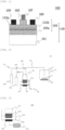

Classifications
-
- H—ELECTRICITY
- H10—SEMICONDUCTOR DEVICES; ELECTRIC SOLID-STATE DEVICES NOT OTHERWISE PROVIDED FOR
- H10D—INORGANIC ELECTRIC SEMICONDUCTOR DEVICES
- H10D62/00—Semiconductor bodies, or regions thereof, of devices having potential barriers
- H10D62/80—Semiconductor bodies, or regions thereof, of devices having potential barriers characterised by the materials
- H10D62/875—Semiconductor bodies, or regions thereof, of devices having potential barriers characterised by the materials being semiconductor metal oxide, e.g. InGaZnO
-
- C—CHEMISTRY; METALLURGY
- C30—CRYSTAL GROWTH
- C30B—SINGLE-CRYSTAL GROWTH; UNIDIRECTIONAL SOLIDIFICATION OF EUTECTIC MATERIAL OR UNIDIRECTIONAL DEMIXING OF EUTECTOID MATERIAL; REFINING BY ZONE-MELTING OF MATERIAL; PRODUCTION OF A HOMOGENEOUS POLYCRYSTALLINE MATERIAL WITH DEFINED STRUCTURE; SINGLE CRYSTALS OR HOMOGENEOUS POLYCRYSTALLINE MATERIAL WITH DEFINED STRUCTURE; AFTER-TREATMENT OF SINGLE CRYSTALS OR A HOMOGENEOUS POLYCRYSTALLINE MATERIAL WITH DEFINED STRUCTURE; APPARATUS THEREFOR
- C30B25/00—Single-crystal growth by chemical reaction of reactive gases, e.g. chemical vapour-deposition growth
- C30B25/02—Epitaxial-layer growth
-
- C—CHEMISTRY; METALLURGY
- C01—INORGANIC CHEMISTRY
- C01G—COMPOUNDS CONTAINING METALS NOT COVERED BY SUBCLASSES C01D OR C01F
- C01G15/00—Compounds of gallium, indium or thallium
-
- C—CHEMISTRY; METALLURGY
- C23—COATING METALLIC MATERIAL; COATING MATERIAL WITH METALLIC MATERIAL; CHEMICAL SURFACE TREATMENT; DIFFUSION TREATMENT OF METALLIC MATERIAL; COATING BY VACUUM EVAPORATION, BY SPUTTERING, BY ION IMPLANTATION OR BY CHEMICAL VAPOUR DEPOSITION, IN GENERAL; INHIBITING CORROSION OF METALLIC MATERIAL OR INCRUSTATION IN GENERAL
- C23C—COATING METALLIC MATERIAL; COATING MATERIAL WITH METALLIC MATERIAL; SURFACE TREATMENT OF METALLIC MATERIAL BY DIFFUSION INTO THE SURFACE, BY CHEMICAL CONVERSION OR SUBSTITUTION; COATING BY VACUUM EVAPORATION, BY SPUTTERING, BY ION IMPLANTATION OR BY CHEMICAL VAPOUR DEPOSITION, IN GENERAL
- C23C16/00—Chemical coating by decomposition of gaseous compounds, without leaving reaction products of surface material in the coating, i.e. chemical vapour deposition [CVD] processes
- C23C16/22—Chemical coating by decomposition of gaseous compounds, without leaving reaction products of surface material in the coating, i.e. chemical vapour deposition [CVD] processes characterised by the deposition of inorganic material, other than metallic material
- C23C16/30—Deposition of compounds, mixtures or solid solutions, e.g. borides, carbides, nitrides
- C23C16/40—Oxides
-
- C—CHEMISTRY; METALLURGY
- C23—COATING METALLIC MATERIAL; COATING MATERIAL WITH METALLIC MATERIAL; CHEMICAL SURFACE TREATMENT; DIFFUSION TREATMENT OF METALLIC MATERIAL; COATING BY VACUUM EVAPORATION, BY SPUTTERING, BY ION IMPLANTATION OR BY CHEMICAL VAPOUR DEPOSITION, IN GENERAL; INHIBITING CORROSION OF METALLIC MATERIAL OR INCRUSTATION IN GENERAL
- C23C—COATING METALLIC MATERIAL; COATING MATERIAL WITH METALLIC MATERIAL; SURFACE TREATMENT OF METALLIC MATERIAL BY DIFFUSION INTO THE SURFACE, BY CHEMICAL CONVERSION OR SUBSTITUTION; COATING BY VACUUM EVAPORATION, BY SPUTTERING, BY ION IMPLANTATION OR BY CHEMICAL VAPOUR DEPOSITION, IN GENERAL
- C23C16/00—Chemical coating by decomposition of gaseous compounds, without leaving reaction products of surface material in the coating, i.e. chemical vapour deposition [CVD] processes
- C23C16/44—Chemical coating by decomposition of gaseous compounds, without leaving reaction products of surface material in the coating, i.e. chemical vapour deposition [CVD] processes characterised by the method of coating
- C23C16/448—Chemical coating by decomposition of gaseous compounds, without leaving reaction products of surface material in the coating, i.e. chemical vapour deposition [CVD] processes characterised by the method of coating characterised by the method used for generating reactive gas streams, e.g. by evaporation or sublimation of precursor materials
- C23C16/4486—Chemical coating by decomposition of gaseous compounds, without leaving reaction products of surface material in the coating, i.e. chemical vapour deposition [CVD] processes characterised by the method of coating characterised by the method used for generating reactive gas streams, e.g. by evaporation or sublimation of precursor materials by producing an aerosol and subsequent evaporation of the droplets or particles
-
- C—CHEMISTRY; METALLURGY
- C30—CRYSTAL GROWTH
- C30B—SINGLE-CRYSTAL GROWTH; UNIDIRECTIONAL SOLIDIFICATION OF EUTECTIC MATERIAL OR UNIDIRECTIONAL DEMIXING OF EUTECTOID MATERIAL; REFINING BY ZONE-MELTING OF MATERIAL; PRODUCTION OF A HOMOGENEOUS POLYCRYSTALLINE MATERIAL WITH DEFINED STRUCTURE; SINGLE CRYSTALS OR HOMOGENEOUS POLYCRYSTALLINE MATERIAL WITH DEFINED STRUCTURE; AFTER-TREATMENT OF SINGLE CRYSTALS OR A HOMOGENEOUS POLYCRYSTALLINE MATERIAL WITH DEFINED STRUCTURE; APPARATUS THEREFOR
- C30B29/00—Single crystals or homogeneous polycrystalline material with defined structure characterised by the material or by their shape
- C30B29/10—Inorganic compounds or compositions
- C30B29/16—Oxides
-
- H—ELECTRICITY
- H10—SEMICONDUCTOR DEVICES; ELECTRIC SOLID-STATE DEVICES NOT OTHERWISE PROVIDED FOR
- H10P—GENERIC PROCESSES OR APPARATUS FOR THE MANUFACTURE OR TREATMENT OF DEVICES COVERED BY CLASS H10
- H10P14/00—Formation of materials, e.g. in the shape of layers or pillars
- H10P14/20—Formation of materials, e.g. in the shape of layers or pillars of semiconductor materials
- H10P14/24—Formation of materials, e.g. in the shape of layers or pillars of semiconductor materials using chemical vapour deposition [CVD]
-
- H—ELECTRICITY
- H10—SEMICONDUCTOR DEVICES; ELECTRIC SOLID-STATE DEVICES NOT OTHERWISE PROVIDED FOR
- H10P—GENERIC PROCESSES OR APPARATUS FOR THE MANUFACTURE OR TREATMENT OF DEVICES COVERED BY CLASS H10
- H10P14/00—Formation of materials, e.g. in the shape of layers or pillars
- H10P14/20—Formation of materials, e.g. in the shape of layers or pillars of semiconductor materials
- H10P14/26—Formation of materials, e.g. in the shape of layers or pillars of semiconductor materials using liquid deposition
- H10P14/265—Formation of materials, e.g. in the shape of layers or pillars of semiconductor materials using liquid deposition using solutions
-
- H—ELECTRICITY
- H10—SEMICONDUCTOR DEVICES; ELECTRIC SOLID-STATE DEVICES NOT OTHERWISE PROVIDED FOR
- H10P—GENERIC PROCESSES OR APPARATUS FOR THE MANUFACTURE OR TREATMENT OF DEVICES COVERED BY CLASS H10
- H10P14/00—Formation of materials, e.g. in the shape of layers or pillars
- H10P14/20—Formation of materials, e.g. in the shape of layers or pillars of semiconductor materials
- H10P14/29—Formation of materials, e.g. in the shape of layers or pillars of semiconductor materials characterised by the substrates
- H10P14/2901—Materials
- H10P14/2921—Materials being crystalline insulating materials
-
- H—ELECTRICITY
- H10—SEMICONDUCTOR DEVICES; ELECTRIC SOLID-STATE DEVICES NOT OTHERWISE PROVIDED FOR
- H10P—GENERIC PROCESSES OR APPARATUS FOR THE MANUFACTURE OR TREATMENT OF DEVICES COVERED BY CLASS H10
- H10P14/00—Formation of materials, e.g. in the shape of layers or pillars
- H10P14/20—Formation of materials, e.g. in the shape of layers or pillars of semiconductor materials
- H10P14/29—Formation of materials, e.g. in the shape of layers or pillars of semiconductor materials characterised by the substrates
- H10P14/2926—Crystal orientations
-
- H—ELECTRICITY
- H10—SEMICONDUCTOR DEVICES; ELECTRIC SOLID-STATE DEVICES NOT OTHERWISE PROVIDED FOR
- H10P—GENERIC PROCESSES OR APPARATUS FOR THE MANUFACTURE OR TREATMENT OF DEVICES COVERED BY CLASS H10
- H10P14/00—Formation of materials, e.g. in the shape of layers or pillars
- H10P14/20—Formation of materials, e.g. in the shape of layers or pillars of semiconductor materials
- H10P14/32—Formation of materials, e.g. in the shape of layers or pillars of semiconductor materials characterised by intermediate layers between substrates and deposited layers
- H10P14/3202—Materials thereof
- H10P14/3234—Materials thereof being oxide semiconducting materials
-
- H—ELECTRICITY
- H10—SEMICONDUCTOR DEVICES; ELECTRIC SOLID-STATE DEVICES NOT OTHERWISE PROVIDED FOR
- H10P—GENERIC PROCESSES OR APPARATUS FOR THE MANUFACTURE OR TREATMENT OF DEVICES COVERED BY CLASS H10
- H10P14/00—Formation of materials, e.g. in the shape of layers or pillars
- H10P14/20—Formation of materials, e.g. in the shape of layers or pillars of semiconductor materials
- H10P14/34—Deposited materials, e.g. layers
- H10P14/3402—Deposited materials, e.g. layers characterised by the chemical composition
- H10P14/3434—Deposited materials, e.g. layers characterised by the chemical composition being oxide semiconductor materials
-
- H—ELECTRICITY
- H10—SEMICONDUCTOR DEVICES; ELECTRIC SOLID-STATE DEVICES NOT OTHERWISE PROVIDED FOR
- H10P—GENERIC PROCESSES OR APPARATUS FOR THE MANUFACTURE OR TREATMENT OF DEVICES COVERED BY CLASS H10
- H10P14/00—Formation of materials, e.g. in the shape of layers or pillars
- H10P14/20—Formation of materials, e.g. in the shape of layers or pillars of semiconductor materials
- H10P14/34—Deposited materials, e.g. layers
- H10P14/3438—Doping during depositing
- H10P14/3441—Conductivity type
- H10P14/3442—N-type
-
- H—ELECTRICITY
- H10—SEMICONDUCTOR DEVICES; ELECTRIC SOLID-STATE DEVICES NOT OTHERWISE PROVIDED FOR
- H10P—GENERIC PROCESSES OR APPARATUS FOR THE MANUFACTURE OR TREATMENT OF DEVICES COVERED BY CLASS H10
- H10P14/00—Formation of materials, e.g. in the shape of layers or pillars
- H10P14/20—Formation of materials, e.g. in the shape of layers or pillars of semiconductor materials
- H10P14/34—Deposited materials, e.g. layers
- H10P14/3438—Doping during depositing
- H10P14/3441—Conductivity type
- H10P14/3444—P-type
-
- H—ELECTRICITY
- H10—SEMICONDUCTOR DEVICES; ELECTRIC SOLID-STATE DEVICES NOT OTHERWISE PROVIDED FOR
- H10P—GENERIC PROCESSES OR APPARATUS FOR THE MANUFACTURE OR TREATMENT OF DEVICES COVERED BY CLASS H10
- H10P14/00—Formation of materials, e.g. in the shape of layers or pillars
- H10P14/20—Formation of materials, e.g. in the shape of layers or pillars of semiconductor materials
- H10P14/34—Deposited materials, e.g. layers
- H10P14/3438—Doping during depositing
- H10P14/3441—Conductivity type
- H10P14/3446—Transition metal elements; Rare earth elements
-
- H—ELECTRICITY
- H10—SEMICONDUCTOR DEVICES; ELECTRIC SOLID-STATE DEVICES NOT OTHERWISE PROVIDED FOR
- H10P—GENERIC PROCESSES OR APPARATUS FOR THE MANUFACTURE OR TREATMENT OF DEVICES COVERED BY CLASS H10
- H10P14/00—Formation of materials, e.g. in the shape of layers or pillars
- H10P14/60—Formation of materials, e.g. in the shape of layers or pillars of insulating materials
-
- H—ELECTRICITY
- H10—SEMICONDUCTOR DEVICES; ELECTRIC SOLID-STATE DEVICES NOT OTHERWISE PROVIDED FOR
- H10P—GENERIC PROCESSES OR APPARATUS FOR THE MANUFACTURE OR TREATMENT OF DEVICES COVERED BY CLASS H10
- H10P14/00—Formation of materials, e.g. in the shape of layers or pillars
- H10P14/60—Formation of materials, e.g. in the shape of layers or pillars of insulating materials
- H10P14/63—Formation of materials, e.g. in the shape of layers or pillars of insulating materials characterised by the formation processes
- H10P14/6326—Deposition processes
- H10P14/6328—Deposition from the gas or vapour phase
- H10P14/6334—Deposition from the gas or vapour phase using decomposition or reaction of gaseous or vapour phase compounds, i.e. chemical vapour deposition
-
- H—ELECTRICITY
- H10—SEMICONDUCTOR DEVICES; ELECTRIC SOLID-STATE DEVICES NOT OTHERWISE PROVIDED FOR
- H10P—GENERIC PROCESSES OR APPARATUS FOR THE MANUFACTURE OR TREATMENT OF DEVICES COVERED BY CLASS H10
- H10P14/00—Formation of materials, e.g. in the shape of layers or pillars
- H10P14/60—Formation of materials, e.g. in the shape of layers or pillars of insulating materials
- H10P14/69—Inorganic materials
- H10P14/692—Inorganic materials composed of oxides, glassy oxides or oxide-based glasses
- H10P14/6938—Inorganic materials composed of oxides, glassy oxides or oxide-based glasses the material containing at least one metal element, e.g. metal oxides, metal oxynitrides or metal oxycarbides
- H10P14/6939—Inorganic materials composed of oxides, glassy oxides or oxide-based glasses the material containing at least one metal element, e.g. metal oxides, metal oxynitrides or metal oxycarbides characterised by the metal
-
- H—ELECTRICITY
- H10—SEMICONDUCTOR DEVICES; ELECTRIC SOLID-STATE DEVICES NOT OTHERWISE PROVIDED FOR
- H10P—GENERIC PROCESSES OR APPARATUS FOR THE MANUFACTURE OR TREATMENT OF DEVICES COVERED BY CLASS H10
- H10P14/00—Formation of materials, e.g. in the shape of layers or pillars
- H10P14/60—Formation of materials, e.g. in the shape of layers or pillars of insulating materials
- H10P14/69—Inorganic materials
- H10P14/692—Inorganic materials composed of oxides, glassy oxides or oxide-based glasses
- H10P14/6938—Inorganic materials composed of oxides, glassy oxides or oxide-based glasses the material containing at least one metal element, e.g. metal oxides, metal oxynitrides or metal oxycarbides
- H10P14/6939—Inorganic materials composed of oxides, glassy oxides or oxide-based glasses the material containing at least one metal element, e.g. metal oxides, metal oxynitrides or metal oxycarbides characterised by the metal
- H10P14/69391—Inorganic materials composed of oxides, glassy oxides or oxide-based glasses the material containing at least one metal element, e.g. metal oxides, metal oxynitrides or metal oxycarbides characterised by the metal the material containing aluminium, e.g. Al2O3
-
- H—ELECTRICITY
- H10—SEMICONDUCTOR DEVICES; ELECTRIC SOLID-STATE DEVICES NOT OTHERWISE PROVIDED FOR
- H10P—GENERIC PROCESSES OR APPARATUS FOR THE MANUFACTURE OR TREATMENT OF DEVICES COVERED BY CLASS H10
- H10P14/00—Formation of materials, e.g. in the shape of layers or pillars
- H10P14/60—Formation of materials, e.g. in the shape of layers or pillars of insulating materials
- H10P14/69—Inorganic materials
- H10P14/692—Inorganic materials composed of oxides, glassy oxides or oxide-based glasses
- H10P14/6938—Inorganic materials composed of oxides, glassy oxides or oxide-based glasses the material containing at least one metal element, e.g. metal oxides, metal oxynitrides or metal oxycarbides
- H10P14/6939—Inorganic materials composed of oxides, glassy oxides or oxide-based glasses the material containing at least one metal element, e.g. metal oxides, metal oxynitrides or metal oxycarbides characterised by the metal
- H10P14/69397—Inorganic materials composed of oxides, glassy oxides or oxide-based glasses the material containing at least one metal element, e.g. metal oxides, metal oxynitrides or metal oxycarbides characterised by the metal the material containing two or more metal elements
-
- H—ELECTRICITY
- H10—SEMICONDUCTOR DEVICES; ELECTRIC SOLID-STATE DEVICES NOT OTHERWISE PROVIDED FOR
- H10D—INORGANIC ELECTRIC SEMICONDUCTOR DEVICES
- H10D30/00—Field-effect transistors [FET]
- H10D30/60—Insulated-gate field-effect transistors [IGFET]
-
- H—ELECTRICITY
- H10—SEMICONDUCTOR DEVICES; ELECTRIC SOLID-STATE DEVICES NOT OTHERWISE PROVIDED FOR
- H10D—INORGANIC ELECTRIC SEMICONDUCTOR DEVICES
- H10D48/00—Individual devices not covered by groups H10D1/00 - H10D44/00
- H10D48/30—Devices controlled by electric currents or voltages
-
- H—ELECTRICITY
- H10—SEMICONDUCTOR DEVICES; ELECTRIC SOLID-STATE DEVICES NOT OTHERWISE PROVIDED FOR
- H10D—INORGANIC ELECTRIC SEMICONDUCTOR DEVICES
- H10D62/00—Semiconductor bodies, or regions thereof, of devices having potential barriers
- H10D62/40—Crystalline structures
-
- H—ELECTRICITY
- H10—SEMICONDUCTOR DEVICES; ELECTRIC SOLID-STATE DEVICES NOT OTHERWISE PROVIDED FOR
- H10P—GENERIC PROCESSES OR APPARATUS FOR THE MANUFACTURE OR TREATMENT OF DEVICES COVERED BY CLASS H10
- H10P14/00—Formation of materials, e.g. in the shape of layers or pillars
- H10P14/20—Formation of materials, e.g. in the shape of layers or pillars of semiconductor materials
- H10P14/32—Formation of materials, e.g. in the shape of layers or pillars of semiconductor materials characterised by intermediate layers between substrates and deposited layers
- H10P14/3202—Materials thereof
- H10P14/3238—Materials thereof being insulating materials
-
- H—ELECTRICITY
- H10—SEMICONDUCTOR DEVICES; ELECTRIC SOLID-STATE DEVICES NOT OTHERWISE PROVIDED FOR
- H10P—GENERIC PROCESSES OR APPARATUS FOR THE MANUFACTURE OR TREATMENT OF DEVICES COVERED BY CLASS H10
- H10P14/00—Formation of materials, e.g. in the shape of layers or pillars
- H10P14/20—Formation of materials, e.g. in the shape of layers or pillars of semiconductor materials
- H10P14/32—Formation of materials, e.g. in the shape of layers or pillars of semiconductor materials characterised by intermediate layers between substrates and deposited layers
- H10P14/3202—Materials thereof
- H10P14/3241—Materials thereof being conductive materials
Definitions
- the present invention relates to a crystalline oxide film, a laminated structure, a semiconductor device, and a method for producing a crystalline oxide film.
- gallium oxide As a switching device for the next generation with achievable high withstand voltage, low losses, and high heat resistance, semiconductor devices using gallium oxide (Ga 2 O 3 ) with a large band gap attract attention and are expected to be applied to power semiconductor devices, such as an inverter.
- gallium oxide can control a band gap by forming mixed crystals with indium or aluminum singly or in combination.
- Patent Document 1 discloses a highly crystalline conductive ⁇ -Ga 2 O 3 thin film with an added dopant (tetravalent tin).
- the thin film disclosed in Patent Document 1 is incapable of maintaining sufficient withstand voltage.
- This film also contains a large amount of carbon impurities and has unsatisfactory semiconductor properties, including conductivity, so the film is still difficult to use for a semiconductor device.
- Patent Document 2 discloses a Ga 2 O 3 -based semiconductor device in which a p-type ⁇ -(Al x Ga 2-x ) 2 O 3 single crystal film is formed on an ⁇ -Al 2 O 3 substrate.
- the semiconductor device disclosed in Patent Document 2 has many limitations to apply the semiconductor devices due to ⁇ -Al 2 O 3 being an insulator or problematic quality of crystals.
- ion implantation and heat treatment at high temperatures are necessary to obtain p-type semiconductors. Consequently, p-type ⁇ -Al 2 O 3 itself is difficult to realize, and in fact, the semiconductor device disclosed in Patent Document 2 as such is difficult to realize.
- Patent Document 3 an SBD (Schottky barrier diode) using ⁇ -Ga 2 O 3 having a thickness of 11.9 um is produced, thereby obtaining a withstand voltage of over 300 V.
- the method for producing the SBD disclosed in Patent Document 3 is a relatively easy method, it is required to make a film thickness thicker than necessary, and reproducibility (i.e., yield) has a problem therein.
- Patent Document 4 an SBD with a surface area of 1 mm square is produced, thereby obtaining a withstand voltage of over 855 V.
- the SBD disclosed in Patent Document 4 needs to use deuterated hydrobromic acid to produce ⁇ -Ga 2 O 3 , which is a semiconductor layer; thus, the problem is that it is economically unfeasible for industrialization.
- An object of the present invention is to provide a crystalline oxide film, a laminated structure, and a semiconductor device with excellent semiconductor properties, particularly excellent withstand voltage while avoiding the above problems. Moreover, an object of the present invention is to provide a method for producing a crystalline oxide film that can produce the crystalline oxide film with excellent semiconductor properties, particularly excellent withstand voltage.
- the present invention provides a crystalline oxide film containing gallium as a main component, wherein when CuK ⁇ rays are made incident on the crystalline oxide film to perform X-ray diffraction,
- the present invention provides a crystalline oxide film containing gallium as a main component, wherein when CuK ⁇ rays are made incident on the crystalline oxide film to perform X-ray diffraction,
- the present invention provides a crystalline oxide film containing gallium as a main component, wherein when CuK ⁇ rays are made incident on the crystalline oxide film to perform X-ray diffraction,
- the present invention provides a crystalline oxide film containing gallium as a main component, wherein when CuK ⁇ rays are made incident on the crystalline oxide film to perform X-ray diffraction,
- Such a crystalline oxide film described above can be obtained with high yield by a simple and easy process and has excellent crystallinity, and semiconductor properties, particularly withstand voltage, when applied to a semiconductor device. In addition, a surface smoothness of the crystalline oxide film is also excellent.
- the crystalline oxide film has a surface area of 100 mm 2 or more or a diameter of 50 mm or more.
- the crystalline oxide film having excellent crystallinity can be obtained over a large surface area.
- the present invention provides a laminated structure at least comprising:
- This provides the laminated structure having excellent crystallinity, and semiconductor properties, particularly withstand voltage, when applied to a semiconductor device.
- a surface smoothness of the film is also excellent.
- the present invention provides a semiconductor device comprising the crystalline oxide film described above.
- the present invention provides a method for producing a crystalline oxide film containing gallium as a main component, the method comprising forming the crystalline oxide film on a sapphire substrate as an underlying substrate, wherein
- the present invention provides a method for producing a crystalline oxide film containing gallium as a main component, the method comprising forming the crystalline oxide film on a sapphire substrate as an underlying substrate, wherein
- the present invention provides a method for producing a crystalline oxide film containing gallium as a main component, the method comprising forming the crystalline oxide film on a sapphire substrate as an underlying substrate, wherein
- the present invention provides a method for producing a crystalline oxide film containing gallium as a main component, the method comprising forming the crystalline oxide film on a sapphire substrate as an underlying substrate, wherein
- the crystalline oxide film can be obtained by an easy and simple process with a high yield. Moreover, the crystalline oxide film can be obtained with excellent crystallinity, and semiconductor properties, particularly withstand voltage, when applied to a semiconductor device. In addition, the crystalline oxide film having a surface smoothness can be obtained.
- the inventive crystalline oxide film has excellent crystallinity, and excellent semiconductor properties, particularly withstand voltage, when applied to a semiconductor device.
- a surface smoothness of the crystalline oxide film is also excellent.
- the laminated structure is provided with excellent crystallinity, and excellent semiconductor properties, particularly withstand voltage when applied to a semiconductor device.
- the surface smoothness of the film is also excellent. Moreover, a leakage current thereof is suppressed.
- the crystalline oxide film can be obtained with excellent crystallinity, and excellent semiconductor properties, particularly withstand voltage when applied to a semiconductor device and also excellent surface smoothness.
- a crystalline oxide film having excellent withstand voltage is required to be provided.
- the present inventors have earnestly studied the above problem and found out that a crystalline oxide film containing gallium as a main component can be obtained with high yield by a simple and easy process and has excellent crystallinity, and excellent semiconductor properties, particularly withstand voltage, when applied to a semiconductor device, in which the crystalline oxide film is provided that, when CuK ⁇ rays are made incident on the crystalline oxide film to perform X-ray diffraction, a reflection output in scanning ⁇ , ⁇ , and 2 ⁇ has a local maximum point when 16.20° ⁇ 2 ⁇ 39.90° and 20.30° ⁇ 32.20°; and 40.10° ⁇ + ⁇ 40.40° relative to ⁇ and ⁇ at which the reflection output reaches a maximum is satisfied. This finding has led to the completion of the present invention.
- the present invention is a crystalline oxide film containing gallium as a main component, in which when CuK ⁇ rays are made incident on the crystalline oxide film to perform X-ray diffraction, a reflection output in scanning ⁇ and 2 ⁇ has a local maximum point when 16.20° ⁇ 2 ⁇ 39.90° and 20.30° ⁇ 32.20° at an angle ⁇ around a ⁇ axis orthogonal to a surface of the crystalline oxide film at the angle ⁇ where a peak attributable to the crystalline oxide film by ⁇ -2 ⁇ measurement is maximum; and 40.10° ⁇ + ⁇ 40.40° relative to ⁇ and ⁇ at which the reflection output reaches a maximum is satisfied.
- the present inventors have earnestly studied the above problem and found out that the crystalline oxide film containing gallium as the main component can be obtained with high yield by a simple and easy process and has excellent crystallinity, and excellent semiconductor properties, particularly withstand voltage, when applied to a semiconductor device, in which the crystalline oxide film is provided that, when CuK ⁇ rays are made incident on the crystalline oxide film to perform X-ray diffraction, the reflection output in scanning ⁇ , ⁇ , and 2 ⁇ has the local maximum point when 26.20° ⁇ 2 ⁇ 49.90° and 25.30° ⁇ 37.20°; and 50.10° ⁇ + ⁇ 50.40° relative to ⁇ and ⁇ at which the reflection output reaches a maximum is satisfied. This finding has led to the completion of the present invention.
- the present invention is a crystalline oxide film containing gallium as a main component, in which when CuK ⁇ rays are made incident on the crystalline oxide film to perform X-ray diffraction, a reflection output in scanning ⁇ and 2 ⁇ has a local maximum point when 26.20° ⁇ 2 ⁇ 49.90° and 25.30° ⁇ 37.20° at an angle ⁇ around a ⁇ axis orthogonal to a surface of the crystalline oxide film at the angle ⁇ where a peak attributable to the crystalline oxide film by ⁇ -2 ⁇ measurement is maximum; and 50.10° ⁇ + ⁇ 50.40° relative to ⁇ and ⁇ at which the reflection output reaches a maximum is satisfied.
- the present inventors have earnestly studied the above problem and found out that the crystalline oxide film containing gallium as the main component can be obtained with high yield by the simple and easy process and has excellent crystallinity, and excellent semiconductor properties, particularly withstand voltage, when applied to a semiconductor device, in which the crystalline oxide film is provided that, when CuK ⁇ rays are made incident on the crystalline oxide film to perform X-ray diffraction, the reflection output in scanning ⁇ , ⁇ , and 2 ⁇ has the local maximum point when 12.00° ⁇ 2 ⁇ 35.70° and 18.20° ⁇ 30.10°; and 35.90° ⁇ + ⁇ 36.20° relative to ⁇ and ⁇ at which the reflection output reaches a maximum is satisfied. This finding has led to the completion of the present invention.
- the present invention is a crystalline oxide film containing gallium as a main component, in which when CuK ⁇ rays are made incident on the crystalline oxide film to perform X-ray diffraction, a reflection output in scanning ⁇ and 2 ⁇ has a local maximum point when 12.00° ⁇ 2 ⁇ 35.70° and 18.20° ⁇ 30.10° at an angle ⁇ around a ⁇ axis orthogonal to a surface of the crystalline oxide film at the angle ⁇ where a peak attributable to the crystalline oxide film by ⁇ -2 ⁇ measurement is maximum; and 35.90° ⁇ + ⁇ 36.20° relative to ⁇ and ⁇ at which the reflection output reaches a maximum is satisfied.
- the present inventors have earnestly studied the above problem and found out that the crystalline oxide film containing gallium as the main component can be obtained with high yield by a simple and easy process and has excellent crystallinity, and excellent semiconductor properties, particularly withstand voltage, when applied to a semiconductor device, in which the crystalline oxide film is provided that, when CuK ⁇ rays are made incident on the crystalline oxide film to perform X-ray diffraction, the reflection output in scanning ⁇ , ⁇ , and 2 ⁇ has the local maximum point when 40.80° ⁇ 2 ⁇ 64.50° and 32.60° ⁇ 44.50°; and 64.70° ⁇ + ⁇ 65.00° relative to ⁇ and ⁇ at which the reflection output reaches a maximum is satisfied. This finding has led to the completion of the present invention.
- the present invention is a crystalline oxide film containing gallium as a main component, in which when CuK ⁇ rays are made incident on the crystalline oxide film to perform X-ray diffraction, a reflection output in scanning ⁇ and 2 ⁇ has a local maximum point when 40.80° ⁇ 2 ⁇ 64.50° and 32.60° ⁇ 44.50° at an angle ⁇ around a ⁇ axis orthogonal to a surface of the crystalline oxide film at the angle ⁇ where a peak attributable to the crystalline oxide film by ⁇ -2 ⁇ measurement is maximum; and 64.70° ⁇ + ⁇ 65.00° relative to ⁇ and ⁇ at which the reflection output reaches a maximum is satisfied.
- the present inventors have earnestly studied the above problem and found out that by forming the crystalline oxide film on the sapphire substrate as the underlying substrate on which CuK ⁇ rays are made incident on the substrate to perform X-ray diffraction, the reflection output in scanning ⁇ , ⁇ , and 2 ⁇ has the local maximum point when 17.70° ⁇ 2 ⁇ 41.40° and 21.00° ⁇ 32.90°, and then 41.60° ⁇ + ⁇ 41.90° relative to w and ⁇ at which the reflection output reaches a maximum is satisfied; the crystalline oxide film can be produced, in which the reflection output in scanning w and 2 ⁇ has the local maximum point when 16.20° ⁇ 2 ⁇ 39.90° and 20.30° ⁇ 32.20°; and 40.10° ⁇ + ⁇ 40.40° relative to ⁇ and ⁇ at which the reflection output reaches a maximum is satisfied, with high yield by a simple and easy process, and the crystalline oxide film obtained has excellent crystallinity, and excellent semiconductor properties, particularly withstand voltage, when applied to
- the present invention is a method for producing a crystalline oxide film containing gallium as a main component, the method includes forming the crystalline oxide film on a sapphire substrate as an underlying substrate, in which when CuK ⁇ rays are made incident on the underlying substrate to perform X-ray diffraction, a reflection output in scanning ⁇ and 2 ⁇ has a local maximum point when 17.70° ⁇ 2 ⁇ 41.40° and 21.00° ⁇ 32.90° at an angle ⁇ around a ⁇ axis orthogonal to a surface of the underlying substrate at the angle ⁇ where a peak attributable to the underlying substrate by ⁇ -2 ⁇ measurement is maximum; and 41.60° ⁇ + ⁇ 41.90° relative to ⁇ and ⁇ at which the reflection output reaches a maximum is satisfied.
- the present inventors have earnestly studied the above problem and found out that by forming the crystalline oxide film on the sapphire substrate as the underlying substrate on which CuK ⁇ rays are made incident on the substrate to perform X-ray diffraction, the reflection output in scanning ⁇ , ⁇ , and 2 ⁇ has the local maximum point when 28.60° ⁇ 2 ⁇ 52.30° and 26.50° ⁇ 38.40°, and then 52.50° ⁇ + ⁇ 52.80° relative to w and ⁇ at which the reflection output reaches a maximum is satisfied; the crystalline oxide film can be produced, in which the reflection output in scanning w and 2 ⁇ has the local maximum point when 26.20° ⁇ 2 ⁇ 49.90° and 25.30° ⁇ 37.20°; and 50.10° ⁇ + ⁇ 50.40° relative to ⁇ and ⁇ at which the reflection output reaches a maximum is satisfied, with high yield by a simple and easy process, and the crystalline oxide film obtained has excellent crystallinity and excellent semiconductor properties, particularly withstand voltage, when applied
- the present invention is a method for producing a crystalline oxide film containing gallium as a main component, the method includes forming the crystalline oxide film on a sapphire substrate as an underlying substrate, in which when CuK ⁇ rays are made incident on the underlying substrate to perform X-ray diffraction, a reflection output in scanning ⁇ and 2 ⁇ has a local maximum point when 28.60° ⁇ 2 ⁇ 52.30° and 26.50° ⁇ 38.40° at an angle ⁇ around a ⁇ axis orthogonal to a surface of the underlying substrate at the angle ⁇ where a peak attributable to the underlying substrate by ⁇ -2 ⁇ measurement is maximum; and 52.50° ⁇ + ⁇ 52.80° relative to ⁇ and ⁇ at which the reflection output reaches a maximum is satisfied.
- the present inventors have earnestly studied the above problem and found out that by forming the crystalline oxide film on the sapphire substrate as the underlying substrate on which CuK ⁇ rays are made incident on the substrate to perform X-ray diffraction, the reflection output in scanning ⁇ , ⁇ , and 2 ⁇ has the local maximum point when 13.80° ⁇ 2 ⁇ 37.50° and 19.10° ⁇ 31.00°, and then 37.70° ⁇ + ⁇ 38.00° relative to w and ⁇ at which the reflection output reaches a maximum is satisfied; the crystalline oxide film can be produced, in which the reflection output in scanning w and 2 ⁇ has the local maximum point when 12.00° ⁇ 2 ⁇ 35.70° and 18.20° ⁇ 30.10°; and 35.90° ⁇ + ⁇ 36.20° relative to ⁇ and ⁇ at which the reflection output reaches a maximum is satisfied, with high yield by a simple and easy process, and the crystalline oxide film obtained has excellent crystallinity and excellent semiconductor properties, particularly withstand voltage, when applied to a semiconductor device.
- the present invention is a method for producing a crystalline oxide film containing gallium as a main component, the method includes forming the crystalline oxide film on a sapphire substrate as an underlying substrate, in which when CuK ⁇ rays are made incident on the underlying substrate to perform X-ray diffraction, a reflection output in scanning ⁇ and 2 ⁇ has a local maximum point when 13.80° ⁇ 2 ⁇ 37.50° and 19.10° ⁇ 31.00° at an angle ⁇ around a ⁇ axis orthogonal to a surface of the underlying substrate at the angle ⁇ where a peak attributable to the underlying substrate by ⁇ -2 ⁇ measurement is maximum; and 37.70° ⁇ + ⁇ 38.00° relative to ⁇ and ⁇ at which the reflection output reaches a maximum is satisfied.
- the present inventors have earnestly studied the above problem and found out that by forming the crystalline oxide film on the sapphire substrate as the underlying substrate on which CuK ⁇ rays are made incident on the substrate to perform X-ray diffraction, the reflection output in scanning ⁇ , ⁇ , and 2 ⁇ has the local maximum point when 44.30° ⁇ 2 ⁇ 68.00° and 34.30° ⁇ 46.20°, and then 68.20° ⁇ + ⁇ 68.50° relative to w and ⁇ at which the reflection output reaches a maximum is satisfied; the crystalline oxide film can be produced, in which a reflection output in scanning ⁇ and 2 ⁇ has the local maximum point when 40.80° ⁇ 2 ⁇ 64.50° and 32.60° ⁇ 44.50°; and 64.70° ⁇ + ⁇ 65.00° relative to ⁇ and ⁇ at which the reflection output reaches a maximum is satisfied, with high yield by a simple and easy process, and the crystalline oxide film obtained has excellent crystallinity, and excellent semiconductor properties, particularly withstand voltage, when
- the present invention is a method for producing a crystalline oxide film containing gallium as a main component, the method includes forming the crystalline oxide film on a sapphire substrate as an underlying substrate, in which when CuK ⁇ rays are made incident on the underlying substrate to perform X-ray diffraction, a reflection output in scanning ⁇ and 2 ⁇ has a local maximum point when 44.30° ⁇ 2 ⁇ 68.00° and 34.30° ⁇ 46.20° at an angle ⁇ around a ⁇ axis orthogonal to a surface of the underlying substrate at the angle ⁇ where a peak attributable to the underlying substrate by ⁇ -2 ⁇ measurement is maximum; and 68.20° ⁇ + ⁇ 68.50° relative to ⁇ and ⁇ at which the reflection output reaches a maximum is satisfied.
- a reflection output in scanning ⁇ , ⁇ , and 2 ⁇ has a local maximum point when 16.20° ⁇ 2 ⁇ 39.90° and 20.30° ⁇ 32.20° when CuK ⁇ rays are made incident to perform X-ray diffraction.
- FIG. 4 shows a conceptual diagram of an X-ray diffraction according to the present invention.
- An X-ray source 402 is to generate CuK ⁇ rays (wavelength 1.5418 ⁇ ).
- An X-ray is made incident to a sample surface of sample 401 through an incidence optical element 403 at an angle ⁇ , and then a reflected X-ray is detected by a detector 405 through a receptive optical element 404 at angle ⁇ relative to the sample surface (a parameter to be controlled is usually 2 ⁇ , twice a value of ⁇ ).
- a ⁇ axis 411 is orthogonal to the sample surface and rotates the sample around the ⁇ axis 411 for an angle ⁇ while maintaining the sample surface horizontal.
- the sample may be manually rotated appropriately.
- scanning is performed where the ⁇ is varied from 0 to 90°, and ⁇ , where a detected intensity reaches a maximum, is searched.
- the ⁇ is fixed at which the detected intensity is the maximum, and then the slit of the detector 405 is narrowed, and then each of 2 ⁇ in a range of 15° to 45°, for example, and w in a range of 15° to 35°, for example, are scanned independently.
- a maximum reflection intensity (reflection output) in this case has the local maximum point when 16.20° ⁇ 2 ⁇ 39.90° and 20.30° ⁇ 32.20°; and 40.10° ⁇ + ⁇ 40.40° relative to ⁇ and ⁇ at which the reflection output reaches a maximum.
- the second invention of the present application is a crystalline oxide film in which when the same measurement described above is performed, a maximum reflection intensity (reflection output) has a local maximum point when 26.20° ⁇ 2 ⁇ 49.90° and 25.30° ⁇ 37.20°; and 50.10° ⁇ + ⁇ 50.40° relative to ⁇ and ⁇ at which the reflection output reaches a maximum is satisfied.
- the third invention of the present application is a crystalline oxide film in which when the same measurement described above is performed, a maximum reflection intensity (reflection output) has a local maximum point when 12.00° ⁇ 2 ⁇ 35.70° and 18.20° ⁇ 30.10°; and 35.90° ⁇ + ⁇ 36.20° relative to ⁇ and ⁇ at which the reflection output reaches a maximum is satisfied.
- the fourth invention of the present application is a crystalline oxide film in which when the same measurement described above is performed, a maximum reflection intensity (reflection output) has a local maximum point when 40.80° ⁇ 2 ⁇ 64.50° and 32.60° ⁇ 44.50°; and 64.70° ⁇ + ⁇ 65.00° relative to ⁇ and ⁇ at which the reflection output reaches a maximum is satisfied.
- a crystal structure of the crystalline oxide film is not particularly limited and may be a ⁇ -gallia structure, a corundum structure, or an orthorhombic crystal. That of the film may be a mixture of a plurality of crystal structures or a polycrystal, but a single crystal or a uniaxially oriented film is preferred.
- the crystalline oxide film according to the present invention is a crystalline oxide film containing gallium as a main component.
- an oxide film is constituted of a metal and oxygen, but in the crystalline oxide film according to the present invention, it is only required that gallium is used as the metal for a main component.
- gallium as a main component means gallium constitutes 50 to 100 atom% of metal components.
- the metal components other than gallium may include one or two or more metals selected from, for example, iron, indium, aluminum, vanadium, titanium, chromium, rhodium, iridium, nickel, and cobalt.
- a dopant element may be included in the crystalline oxide film.
- n-type dopants such as tin, germanium, silicon, titanium, zirconium, vanadium, or niobium
- p-type dopants such as copper, silver, tin, iridium, rhodium, or magnesium
- a concentration of the dopant may be, for example, about 1 ⁇ 10 16 /cm 3 to 1 ⁇ 10 22 /cm 3 , or may be a low concentration of about 1 ⁇ 10 17 /cm 3 or less, or a high concentration of about 1 ⁇ 10 20 /cm 3 or more.
- a film thickness of the crystalline oxide film is not particularly limited, but 1 um or more is preferable.
- the upper limit thereof is not particularly limited.
- the thickness may be, for example, 100 um or less, and can be preferably 50 um or less, and more preferably 20 um or less.
- a size of the crystalline oxide film is not particularly restricted, but it is preferable to have a surface area of the crystalline oxide film of 100 mm 2 or more or a diameter of 2 inches (50mm) or more, because the film having excellent crystallinity and large surface can be obtained.
- Such a crystalline oxide film according to the present invention can be obtained with high yield by a simple and easy process as described later.
- FIG. 1 shows a suitable example of a semiconductor device 100 in which a laminated structure 110 according to the present invention is used. As shown in FIG. 1 , the laminated structure 110 according to the present invention has an underlying substrate 101 and any of a crystalline oxide films 103 described above.
- the buffer layer may be any of the crystalline oxide film, a semiconductor film, an insulator film, a metal film, or the like.
- Al 2 O 3 , Ga 2 O 3 , Cr 2 O 3 , Fe 2 O 3 , In 2 O 3 , Rh 2 O 3 , V 2 O 3 , Ti 2 O 3 , or Ir 2 O 3 , or the like are suitably used and a solid solution thereof may be used.
- the buffer layer has a thickness of preferably 0.1 um to 2 ⁇ m.
- the underlying substrate 101 in the laminated structure 110 according to the present invention is not particularly limited as long as the substrate is suitable for growing the crystalline oxide film 103 described above and servable as a support.
- a material thereof is not particularly limited, and a known substrate may be used; the material may be an organic compound or may be an inorganic compound.
- polysulfone, polyethersulfone, polyphenylene sulfide, polyetheretherketone, polyimide, polyetherimide, fluororesin, metals such as iron, aluminum, stainless steel, and gold, quartz, glass, calcium carbonate, gallium oxide, and ZnO are exemplified.
- single-crystal substrates such as silicon, sapphire, lithium tantalate, lithium niobate, SiC, GaN, iron oxide, and chromium oxide are exemplified, and single-crystal substrates such as the above are desirable for the laminated structure 110 according to the present invention. In this way, better quality crystalline oxide film 103 can be obtained.
- a sapphire substrate, a lithium tantalate substrate, and a lithium niobate substrate are relatively inexpensive and industrially advantageous.
- the underlying substrate that is suitable for the growth is selected.
- the underlying substrate has a thickness of 100 to 5000 um. With such a range, handling is easy, and a good-quality film can be easily obtained because thermal resistance can be suppressed during the forming.
- the crystalline oxide film 103 is formed on the underlying substrate 101.
- the crystalline oxide film 103 is constituted by an insulator thin film 103a and a conductive thin film 103b laminated in this order from the underlying substrate 101 side.
- a gate insulator film 105 is formed on the conductive thin film 103b.
- a gate electrode 107 is formed on the gate insulator film 105.
- a source-drain electrode 109 is formed on the conductive thin film 103b so as to sandwich the gate electrode 107.
- a depletion layer formed in the conductive thin film 103b can be controlled by a gate voltage applied to the gate electrode 107, and thus transistor action (FET device) is enabled.
- the transistor such as an MIS, a HEMT, an IGBT, and the like; a TFT, a Schottky barrier diode using semiconductor-metal junction, a PN or PIN diode combined with other P layers, and a light receiving and light emitting device is exemplified.
- the laminated structure according to the present invention is useful for improving characteristics of these devices.
- Such a laminated structure described above can be formed by known methods such as an evaporation method, an MBE method, a sputtering method, a CVD method, a mist CVD method, and a liquid phase epitaxy.
- mist in the present invention is a generic term for fine liquid particles dispersed in a gas, including those called fog, droplets, etc.
- FIG. 2 shows an example of a film forming apparatus 201 used in the mist CVD method.
- the film forming apparatus 201 includes at least a mist-forming unit 220 for forming a raw material solution 204a into the mist to generate the mist; a carrier gas supply unit 230 for supplying a carrier gas to transport the mist; a supply pipe 209 connecting the mist-forming unit 220 and a film forming chamber 207 to transport the mist by the carrier gas; and the film forming chamber 207 for heat treating the mist supplied with the carrier gas from the supply pipe 209 to form on the underlying substrate 210.
- the raw material solution 204a is formed into the mist to generate the mist.
- the mist-forming method is not particularly limited as long as the raw material solution 204a can be formed into the mist.
- a known mist-forming means may be applicable, but the mist-forming means using ultrasonic vibrations is preferable. This is because stabler mist-forming can be performed.
- FIG. 3 shows an example of such a mist-forming unit 220.
- the mist-forming unit 220 may include a mist-generating source 204 accommodating the raw material solution 204a therein; a container 205 that can accommodate a medium capable of transmitting ultrasonic vibrations, for example, water 205a; and an ultrasonic vibrator 206 attached on the bottom surface of the container 205.
- the mist generating source 204 made of a container accommodating the raw material solution 204a can be accommodated with a support (not shown) in the container 205 accommodating water 205a.
- the ultrasonic vibrator 206 may be provided on the bottom of the container 205, and the ultrasonic vibrator 206 and an oscillator 216 may be connected.
- the ultrasonic vibrator 206 is vibrated to propagate the ultrasonic waves into the mist generating source 204 via water 205a, and thus the raw material solution 204a is formed into the mist.
- the material contained in the raw material solution 204a may be inorganic or organic material, and the material contained in the solution is not particularly limited as long as gallium is contained therein and the solution can be formed into the mist.
- a metal or a metal compound is suitably used, and those containing one or two or more metals selected from iron, indium, aluminum, vanadium, titanium, chromium, rhodium, nickel, and cobalt may be used, for example.
- the metal dissolved or dispersed in an organic solvent or water in a form of a complex or a salt can be suitably used.
- halogenated salts such as metal chloride salt, metal bromide salt, and metal iodide salts can be exemplified.
- the above metals dissolved in, for example, hydrogen halides such as hydrobromic acid, hydrochloric acid, and hydroiodic acid can also be used as a salt solution.
- complex for example, acetylacetonate complex, carbonyl complex, ammine complex, hydride complex and the like are exemplified.
- the acetylacetonate complex can also be formed by mixing acetylacetone with the salt solution described above.
- a metal concentration in the raw material solution 204a is not particularly limited and can be 0.005 to 1 mol/L, etc.
- a temperature during mixing and dissolving is preferably 20°C or higher.
- the raw material solution may be mixed with additives such as hydrohalic acid and an oxidizing agent.
- hydrohalic acid for example, hydrobromic acid, hydrochloric acid, and hydroiodic acid are exemplified, of which hydrobromic acid or hydroiodic acid is preferred.
- peroxides such as hydrogen peroxide (H 2 O 2 ), sodium peroxide (Na 2 O 2 ), barium peroxide (BaO 2 ), benzoyl peroxide (C 6 H 5 CO) 2 O 2 ; organic peroxides such as hypochlorous acid (HClO), perchloric acid, nitric acid, ozone water, peracetic acid, and nitrobenzene are exemplified.
- peroxides such as hydrogen peroxide (H 2 O 2 ), sodium peroxide (Na 2 O 2 ), barium peroxide (BaO 2 ), benzoyl peroxide (C 6 H 5 CO) 2 O 2 ; organic peroxides such as hypochlorous acid (HClO), perchloric acid, nitric acid, ozone water, peracetic acid, and nitrobenzene are exemplified.
- the raw material solution may contain a dopant.
- the type of dopant is not particularly limited.
- n-type dopants such as tin, germanium, silicon, titanium, zirconium, vanadium, or niobium
- p-type dopants such as copper, silver, iridium, rhodium, or magnesium are exemplified.
- the carrier gas supply unit 230 has a carrier gas source 202a to supply the carrier gas.
- a flow regulating valve 203a may be provided to regulate a flow rate of the carrier gas delivered from the carrier gas source 202a.
- the supply unit can be provided as needed with a diluent carrier gas source 202b to supply diluent carrier gas or a flow regulating valve 203b to regulate the flow rate of the diluent carrier gas delivered from the diluent carrier gas source 202b.
- a type of carrier gas is not particularly limited and can be selected as appropriate for a film to be formed.
- oxygen, ozone, inert gases such as nitrogen and argon, as well as reducing gases such as hydrogen gas and forming gas are exemplified.
- the type of carrier gas may be one type or two or more types.
- a diluted gas in which the same gas as a first carrier gas is diluted with another gas (e.g., diluted 10 times) may be further used as the second carrier gas, or air may be used.
- the flow rate of the carrier gas is not particularly limited.
- the flow rate of the carrier gas is preferably 0.05 to 50 L/min and more preferably 5 to 20 L/min.
- the film forming apparatus 201 has the supply pipe 209 to connect the mist-forming unit 220 and the film forming chamber 207.
- the mist is transported by the carrier gas from the mist generating source 204 of the mist-forming unit 220 via the supply pipe 209 and supplied into the film forming chamber 207.
- a quartz tube, a glass tube, and a tube made of resin can be used for the supply pipe 209.
- the underlying substrate 210 is placed in the film forming chamber 207, where a heater 208 can be provided to heat the underlying substrate 210.
- the heater 208 may be provided on an outside of the film forming chamber 207 as shown in FIG. 2 or may be provided on an inside of the film forming chamber 207.
- the mist supplied from the supply pipe 209 passes through the piping in the film forming chamber 207 and is sprayed with carrier gas from a nozzle onto the underlying substrate 210.
- the film forming chamber 207 may be provided with an exhaust port 212 for exhaust gas at a position where the mist supply to the underlying substrate 210 is not affected.
- the underlying substrate 210 may be placed on a top surface of the film forming chamber 207, for example, to make the substrate face down, or the underlying substrate 210 may be placed on a bottom surface of the film forming chamber 207 to make the substrate face up.
- an underlying substrate used for film growth is an underlying substrate in which maximum reflection intensity (reflection output) appears (having a local maximum point) at a certain range of 2 ⁇ and w when ⁇ , ⁇ , and 2 ⁇ are scanned with CuK ⁇ rays as X-rays generated from the X-ray source as described above.
- the substrate when sapphire is used for the underlying substrate, it is acceptable to use the substrate in which the maximum reflection intensity appears when 17.70° ⁇ 2 ⁇ 41.40° and 21.00° ⁇ 32.90°. In this case, 41.60° ⁇ + ⁇ 41.90° is preferable.
- the crystalline oxide film can be produced in which a reflection output in scanning ⁇ and 2 ⁇ has a local maximum point when 16.20° ⁇ 2 ⁇ 39.90° and 20.30° ⁇ 32.20°; and 40.10° ⁇ + ⁇ 40.40° relative to ⁇ and ⁇ at which the reflection output reaches a maximum is satisfied.
- the substrate when sapphire is used for the underlying substrate, it is acceptable to use the substrate in which the maximum reflection intensity appears when 28.60° ⁇ 2 ⁇ 52.30° and 26.50° ⁇ 38.40°. In this case, 52.50° ⁇ + ⁇ 52.80° is preferable.
- the crystalline oxide film can be produced in which a reflection output in scanning ⁇ and 2 ⁇ has a local maximum point when 26.20° ⁇ 2 ⁇ 49.90°and 25.30° ⁇ 37.20°; and 50.10° ⁇ + ⁇ 50.40° relative to ⁇ and ⁇ at which the reflection output reaches a maximum is satisfied.
- the crystalline oxide film can be produced in which a reflection output in scanning ⁇ and 2 ⁇ has a local maximum point when 12.00° ⁇ 2 ⁇ 35.70° and 18.20° ⁇ 30.10°; and 35.90° ⁇ + ⁇ 36.20° relative to ⁇ and ⁇ at which the reflection output reaches a maximum is satisfied.
- the substrate when sapphire is used for the underlying substrate, it is acceptable to use the substrate in which the maximum reflection intensity appears at 44.30° ⁇ 2 ⁇ 68.00° and 34.30° ⁇ 46.20°. In this case, 68.20° ⁇ + ⁇ 68.50° is preferable.
- the crystalline oxide film can be produced in which a reflection output in scanning ⁇ and 2 ⁇ has a local maximum point when 40.80° ⁇ 2 ⁇ 64.50° and 32.60° ⁇ 44.50°; and 64.70° ⁇ + ⁇ 65.00° relative to ⁇ and ⁇ at which the reflection output reaches a maximum is satisfied.
- the substrate when lithium tantalate is used for the underlying substrate, it is acceptable to use the substrate in which the maximum reflection intensity appears at 15.20° ⁇ 2 ⁇ 38.90° and 19.80° ⁇ 31.70°. In this case, 39.10° ⁇ + ⁇ 39.40° is preferable. Also, by using such an underlying substrate, the crystalline oxide film can be produced in which a reflection output in scanning ⁇ and 2 ⁇ has a local maximum point when 16.20° ⁇ 2 ⁇ 39.90° and 20.30° ⁇ 32.20°; and 40.10° ⁇ + ⁇ 40.40° relative to ⁇ and ⁇ at which the reflection output reaches a maximum is satisfied.
- the crystalline oxide film can be produced in which a reflection output in scanning ⁇ and 2 ⁇ has a local maximum point when 26.20° ⁇ 2 ⁇ 49.90° and 25.30° ⁇ 37.20°; and 50.10° ⁇ + ⁇ 50.40° relative to ⁇ and ⁇ at which the reflection output reaches a maximum is satisfied.
- the substrate when lithium tantalate is used for the underlying substrate, it is acceptable to use the substrate in which the maximum reflection intensity appears at 10.80° ⁇ 2 ⁇ 34.50° and 17.60° ⁇ 29.50°. In this case, 34.70° ⁇ + ⁇ 35.00° is preferable. Also, by using such an underlying substrate, the crystalline oxide film can be produced in which a reflection output in scanning ⁇ and 2 ⁇ has a local maximum point when 12.00° ⁇ 2 ⁇ 35.70° and 18.20° ⁇ 30.10°; and 35.90° ⁇ + ⁇ 36.20° relative to ⁇ and ⁇ at which the reflection output reaches a maximum is satisfied.
- the crystalline oxide film can be produced in which a reflection output in scanning ⁇ and 2 ⁇ has a local maximum point when 40.80° ⁇ 2 ⁇ 64.50° and 32.60° ⁇ 44.50°; and 64.70° ⁇ + ⁇ 65.00° relative to ⁇ and ⁇ at which the reflection output reaches a maximum is satisfied.
- the film By forming the film using such an underlying substrate, the film can be grown inheriting from information of the underlying substrate, and the crystalline oxide film according to the present invention can be obtained.
- Such an underlying substrate can be obtained, for example, by providing a substrate with a finely varied plane orientation of the film-forming surface of the underlying substrate and selecting such an underlying substrate described above by X-ray diffraction measurement.
- the mist CVD method includes a step of generating the mist by forming the material solution into the mist, in which the solution contains gallium, in a mist forming unit; a step of supplying the carrier gas to supply the carrier gas, which transports the mist, to the mist-forming unit; a step of transporting to transport the mist by the carrier gas from the mist-forming unit to the film forming chamber via a supply pipe connecting the mist-forming unit and a film forming chamber; and a step of film forming in which the mist transported is heat treated to form a film on an underlying substrate.
- the raw material solution 204a mixed as described above is accommodated in the mist generating source 204, the underlying substrate 210 is placed in the film forming chamber 207, and then the heater 208 is operated. Next, flow regulating valves 203a and 203b are opened to supply the carrier gas from the carrier gas source 202a and the diluent carrier gas source 202b into the film forming chamber 207, and then an atmosphere in the film forming chamber 207 is sufficiently replaced with the carrier gas, after that, the flow rates of the carrier gas and the flow rate of the diluent carrier gas are adjusted, respectively.
- the ultrasonic vibrator 206 is vibrated, and the vibration is propagated to the raw material solution 204a through the water 205a to form the raw material solution 204a into the mist and generate the mist.
- the carrier gas for transporting the mist is supplied to the mist-forming unit 220.
- the mist is transported by the carrier gas from the mist-forming unit 220 to the film forming chamber 207 via the supply pipe 209 connecting the mist-forming unit 220 to the film forming chamber 207.
- the mist transported to the film forming chamber 207 is heated to generate a thermal reaction, thereby forming the film on a part of or an entire surface of the underlying substrate 210.
- the thermal reaction requires that the reaction of gallium and the like contained in the mist proceed by heating. Therefore, it is required to make a temperature of the substrate surface at the time of the reaction at least 400°C or higher.
- the mist CVD method requires making the raw material reach the underlying substrate surface in the form of liquid in the mist shape. Consequently, the temperature of the underlying substrate surface drops significantly. Thus, the temperature of the underlying substrate surface during the reaction is different from a preset temperature of the apparatus.
- the temperature of the underlying substrate surface during the reaction can be measured to substitute by making a simulation of the state of the reaction by, for example, introducing only carrier gas or water mist containing no solutes.
- the thermal reaction also depends on a temperature of the environment surrounding the underlying substrate. Consequently, a temperature of a nozzle or an inner wall of the film forming chamber is desirably higher than a room temperature. This is because the thermal reaction described above is stabilized.
- the nozzle temperature can be 50 to 250°C.
- the thermal reaction may be performed in any atmosphere of a vacuum, a non-oxygen atmosphere, a reducing gas atmosphere, an air atmosphere, and an oxygen atmosphere, and may be determined appropriately depending on the film to be formed.
- a reaction pressure can be under any conditions of atmospheric pressure, pressurized pressure, or depressurized pressure, but the film forming under atmospheric pressure is preferable because an apparatus configuration is simplified.
- the buffer layer may be provided between the underlying substrate and the crystalline oxide film as appropriate.
- a forming method of the buffer layer is not particularly limited, and the layer can be formed by known methods such as the sputtering method or a deposition method. However, in a case where the mist CVD method described above is used, the layer can be formed by changing the raw material solution as appropriate, thus making the formation thereof simple and easy. Specifically, one or two or more metals selected from aluminum, gallium, chromium, iron, indium, rhodium, vanadium, titanium, and iridium, dissolved or dispersed in water in the form of complexes or salts, can be suitably used as a raw material aqueous solution.
- the complex for example, an acetylacetonate complex, a carbonyl complex, an ammine complex, a hydride complex, and the like are exemplified.
- salt for example, metal chloride salt, metal bromide salt, metal iodide salt, and the like are exemplified.
- the above metals dissolved in hydrobromic acid, hydrochloric acid, hydroiodic acid, and the like can also be used as an aqueous salt solution.
- a solute concentration is preferably 0.005 to 1 mol/L, and a dissolution temperature is preferably 20°C or higher.
- the buffer layer can be formed by making the conditions the same as described above. After the buffer layer is formed to have a predetermined thickness, the film forming is performed by the above method.
- a special case in the buffer layer forming method is a case in which the same material with the crystalline oxide film is used.
- a forming temperature of the buffer layer may be higher than a forming temperature of the crystalline oxide film.
- the forming temperature of the buffer layer may be 450°C and the forming temperature of the crystalline oxide film 400°C, or that of the buffer layer forming may be 500°C and the crystalline oxide film 450°C. This further improves the crystallinity of the crystalline oxide film.
- the laminated structure according to the present invention may be heat treated at 200 to 600°C.
- the heat treatment may be performed in air, an oxygen atmosphere, or an inert gas atmosphere such as nitrogen or argon.
- the heat treatment time is determined as appropriate and can be, for example, 5 to 240 minutes.
- the crystalline oxide film may be delaminated from the underlying substrate.
- a delaminating means is not particularly limited and may be a known means.
- a method for the delaminating means for example, means to delaminate by applying mechanical shock, means to delaminate by applying heat to utilize thermal stress, means to delaminate by applying vibration such as an ultrasonic wave, and means to delaminate by etching are exemplified.
- the crystalline oxide film can be obtained as a freestanding film.
- the crystalline oxide film according to the present invention can also be produced by methods other than the mist CVD method. In this way, the inventive crystalline oxide film can be obtained with high yield by a simple and easy process.
- the film forming apparatus 201 was provided with a carrier gas source 202a to supply a carrier gas; a flow regulating valve 203a to regulate a flow rate of the carrier gas delivered from the carrier gas source 202a; a diluent carrier gas source 202b to supply a diluent carrier gas; a flow regulating valve 203b to regulate a flow rate of the diluent carrier gas delivered from the diluent carrier gas source 202b; a mist generating source 204 storing raw material solution 204a therein; a container 205 accommodating water 205a therein; an ultrasonic vibrator 206 attached on a bottom surface of the container 205; a film forming chamber 207 including a heater 208; and a supply pipe 209 made of quartz connecting the mist generating source 204 to the film forming chamber 207.
- a sapphire substrate having 4 inches (100mm) was provided as an underlying substrate 210.
- This underlying substrate 210 was placed in the film forming chamber 207, the heater 208 was set to 450°C, the temperature was raised, and the chamber was left for 30 minutes to stabilize the temperature inside the film forming chamber including a nozzle.
- the raw material solution 204a As for the raw material solution 204a, ultrapure water was used as the solvent, and gallium bromide as the solute. A gallium concentration in the raw material solution was set to 0.1 mol/L, and tin bromide was mixed so as to make the atomic ratio of tin to gallium 1:0.08. This raw material solution 204a was accommodated in the mist generating source 204. Subsequently, the flow regulating valves 203a and 203b were opened to supply the carrier gas from the carrier gas source 202a and the diluent carrier gas source 202b into the film forming chamber 207.
- the flow rate of the carrier gas was adjusted to 2 L/min and the flow rate of the diluent carrier gas to 6 L/min. Nitrogen was used as the carrier gas and the diluent carrier gas.
- the ultrasonic vibrator 206 was vibrated at 2.4 MHz, and the vibration was propagated through the water 205a to the raw material solution 204a to form the raw material solution 204a into the mist to generate the mist.
- This mist was introduced into the film forming chamber 207 through the supply pipe 209 by the carrier gas, and the mist was thermally reacted on the underlying substrate 210 to form a thin film made of gallium oxide on the underlying substrate 210.
- the forming time was 180 minutes.
- the formation of ⁇ -Ga 2 O 3 was confirmed by X-ray diffraction.
- the film thickness was measured with an optical interferotype film thickness meter and was 7.8 ⁇ m.
- n + type semiconductor film which was delaminated from the sapphire substrate was placed in the film forming chamber 207, and then the heater 208 was set to 450°C, the temperature was raised, and the chamber was left for 30 minutes to stabilize the temperature in the film forming chamber including the nozzle.
- the raw material solution 204a As for the raw material solution 204a, ultrapure water was used as the solvent, and gallium bromide as the solute. A gallium concentration in the raw material solution was set to 0.1 mol/L.
- This raw material solution 204a was accommodated in the mist generating source 204.
- the flow regulating valves 203a and 203b were opened to supply the carrier gas from the carrier gas source 202a and the diluent carrier gas source 202b into the film forming chamber 207. After an atmosphere in the film forming chamber 207 was sufficiently replaced with the carrier gas, the flow rate of the carrier gas was adjusted to 2 L/min and the flow rate of the diluent carrier gas to 6 L/min. Nitrogen was used as the carrier gas and the diluent carrier gas.
- the ultrasonic vibrator 206 was vibrated at 2.4 MHz, and the vibration was propagated through the water 205a to the raw material solution 204a to form the raw material solution 204a into the mist to generate the mist.
- This mist was introduced into the film forming chamber 207 through the supply pipe 209 by the carrier gas, and the mist was thermally reacted on the underlying substrate 210 to form a thin film made of gallium oxide on the underlying substrate 210.
- the forming time was 120 minutes.
- ⁇ -Ga 2 O 3 the formation of ⁇ -Ga 2 O 3 was confirmed by X-ray diffraction.
- a Pt layer, a Ti layer, and an Au layer were laminated on an n - -type semiconductor layer by electron beam evaporation, respectively. Note that the Pt layer had a thickness of 10 nm, the Ti layer had a thickness of 4 nm, and the Au layer had a thickness of 175 nm.
- a Ti layer and an Au layer were laminated on an n + -type semiconductor layer by electron beam evaporation, respectively. Note that the Ti layer had a thickness of 35 nm, and the Au layer had a thickness of 175 nm.
- 82% was acceptable.
- 80% was acceptable.
- 90% was acceptable.
- 83% was acceptable.
- 85% was acceptable.
- 32% was acceptable.
- 83% was acceptable.
- 80% was acceptable.
- 87% was acceptable.
- 82% was acceptable.
Landscapes
- Chemical & Material Sciences (AREA)
- Organic Chemistry (AREA)
- Materials Engineering (AREA)
- Metallurgy (AREA)
- Engineering & Computer Science (AREA)
- Inorganic Chemistry (AREA)
- Crystallography & Structural Chemistry (AREA)
- Chemical Kinetics & Catalysis (AREA)
- General Chemical & Material Sciences (AREA)
- Mechanical Engineering (AREA)
- Dispersion Chemistry (AREA)
- Crystals, And After-Treatments Of Crystals (AREA)
- Thin Film Transistor (AREA)
- Recrystallisation Techniques (AREA)
- Laminated Bodies (AREA)
Abstract
Description
- The present invention relates to a crystalline oxide film, a laminated structure, a semiconductor device, and a method for producing a crystalline oxide film.
- As a switching device for the next generation with achievable high withstand voltage, low losses, and high heat resistance, semiconductor devices using gallium oxide (Ga2O3) with a large band gap attract attention and are expected to be applied to power semiconductor devices, such as an inverter. Such gallium oxide can control a band gap by forming mixed crystals with indium or aluminum singly or in combination. Among all, InAlGaO-based semiconductors represented by Inx'Aly'Gaz'O3 (0≤X'≤2, 0≤Y'≤2, 0≤Z'≤2, X'+Y'+Z'=1.5 to 2.5) are extremely attractive materials.
-
- Patent Document 1:
JP 2013-028480 A - Patent Document 2:
JP 2013-058637 A - Patent Document 3:
WO 2016/013554 A1 - Patent Document 4:
JP 2018-129500 A - Patent Document 1 discloses a highly crystalline conductive α-Ga2O3 thin film with an added dopant (tetravalent tin). However, the thin film disclosed in Patent Document 1 is incapable of maintaining sufficient withstand voltage. This film also contains a large amount of carbon impurities and has unsatisfactory semiconductor properties, including conductivity, so the film is still difficult to use for a semiconductor device.
- Patent Document 2 discloses a Ga2O3-based semiconductor device in which a p-type α-(AlxGa2-x)2O3 single crystal film is formed on an α-Al2O3 substrate. However, the semiconductor device disclosed in Patent Document 2 has many limitations to apply the semiconductor devices due to α-Al2O3 being an insulator or problematic quality of crystals. In addition, in an MBE method, ion implantation and heat treatment at high temperatures are necessary to obtain p-type semiconductors. Consequently, p-type α-Al2O3 itself is difficult to realize, and in fact, the semiconductor device disclosed in Patent Document 2 as such is difficult to realize.
- As a response to these issues, in
Patent Document 3, an SBD (Schottky barrier diode) using α-Ga2O3 having a thickness of 11.9 um is produced, thereby obtaining a withstand voltage of over 300 V. Although the method for producing the SBD disclosed inPatent Document 3 is a relatively easy method, it is required to make a film thickness thicker than necessary, and reproducibility (i.e., yield) has a problem therein. - In
Patent Document 4, an SBD with a surface area of 1 mm square is produced, thereby obtaining a withstand voltage of over 855 V. However, the SBD disclosed inPatent Document 4 needs to use deuterated hydrobromic acid to produce α-Ga2O3, which is a semiconductor layer; thus, the problem is that it is economically unfeasible for industrialization. - An object of the present invention is to provide a crystalline oxide film, a laminated structure, and a semiconductor device with excellent semiconductor properties, particularly excellent withstand voltage while avoiding the above problems. Moreover, an object of the present invention is to provide a method for producing a crystalline oxide film that can produce the crystalline oxide film with excellent semiconductor properties, particularly excellent withstand voltage.
- To solve the above problem, the present invention provides a crystalline oxide film containing gallium as a main component, wherein when CuKα rays are made incident on the crystalline oxide film to perform X-ray diffraction,
- a reflection output in scanning ω and 2Θ has a local maximum point when 16.20°<2Θ<39.90° and 20.30°<ω<32.20° at an angle ϕ around a ϕ axis orthogonal to a surface of the crystalline oxide film at the angle ϕ where a peak attributable to the crystalline oxide film by ω-2θ measurement is maximum, and
- 40.10°<ω+θ<40.40° relative to ω and θ at which the reflection output reaches a maximum is satisfied.
- In addition, the present invention provides a crystalline oxide film containing gallium as a main component, wherein when CuKα rays are made incident on the crystalline oxide film to perform X-ray diffraction,
- a reflection output in scanning ω and 2Θ has a local maximum point when 26.20°<2Θ<49.90° and 25.30°<ω<37.20° at an angle ϕ around a ϕ axis orthogonal to a surface of the crystalline oxide film at the angle ϕ where a peak attributable to the crystalline oxide film by ω-2θ measurement is maximum, and
- 50.10°<ω+θ<50.40° relative to ω and θ at which the reflection output reaches a maximum is satisfied.
- Moreover, the present invention provides a crystalline oxide film containing gallium as a main component, wherein when CuKα rays are made incident on the crystalline oxide film to perform X-ray diffraction,
- a reflection output in scanning ω and 2Θ has a local maximum point when 12.00°<2Θ<35.70° and 18.20°<ω<30.10° at an angle ϕ around a ϕ axis orthogonal to a surface of the crystalline oxide film at the angle ϕ where a peak attributable to the crystalline oxide film by ω-2θ measurement is maximum, and
- 35.90°<ω+θ<36.20° relative to ω and θ at which the reflection output reaches a maximum is satisfied.
- Furthermore, the present invention provides a crystalline oxide film containing gallium as a main component, wherein when CuKα rays are made incident on the crystalline oxide film to perform X-ray diffraction,
- a reflection output in scanning ω and 2Θ has a local maximum point when 40.80°<2θ<64.50° and 32.60°<ω<44.50° at an angle ϕ around a ϕ axis orthogonal to a surface of the crystalline oxide film at the angle ϕ where a peak attributable to the crystalline oxide film by ω-2θ measurement is maximum, and
- 64.70°<ω+θ<65.00° relative to ω and θ at which the reflection output reaches a maximum is satisfied.
- Such a crystalline oxide film described above can be obtained with high yield by a simple and easy process and has excellent crystallinity, and semiconductor properties, particularly withstand voltage, when applied to a semiconductor device. In addition, a surface smoothness of the crystalline oxide film is also excellent.
- In addition, in the present invention, it is preferable that the crystalline oxide film has a surface area of 100 mm2 or more or a diameter of 50 mm or more.
- As a result, the crystalline oxide film having excellent crystallinity can be obtained over a large surface area.
- Moreover, the present invention provides a laminated structure at least comprising:
- an underlying substrate; and
- the crystalline oxide film described above.
- This provides the laminated structure having excellent crystallinity, and semiconductor properties, particularly withstand voltage, when applied to a semiconductor device. In addition, a surface smoothness of the film is also excellent.
- Moreover, the present invention provides a semiconductor device comprising the crystalline oxide film described above.
- This provides the semiconductor device having excellent semiconductor properties, particularly withstand voltage.
- In addition, the present invention provides a method for producing a crystalline oxide film containing gallium as a main component, the method comprising forming the crystalline oxide film on a sapphire substrate as an underlying substrate, wherein
- when CuKα rays are made incident on the underlying substrate to perform X-ray diffraction,
- a reflection output in scanning ω and 2Θ has a local maximum point when 17.70°<2θ<41.40° and 21.00°<ω<32.90° at an angle ϕ around a ϕ axis orthogonal to a surface of the underlying substrate at the angle ϕ where a peak attributable to the crystalline oxide film by ω-2θ measurement is maximum, and
- 41.60°<ω+θ<41.90° relative to ω and θ at which the reflection output reaches a maximum is satisfied.
- Moreover, the present invention provides a method for producing a crystalline oxide film containing gallium as a main component, the method comprising forming the crystalline oxide film on a sapphire substrate as an underlying substrate, wherein
- when CuKα rays are made incident on the underlying substrate to perform X-ray diffraction,
- a reflection output in scanning ω and 2Θ has a local maximum point when 28.60°<2θ<52.30° and 26.50°<ω<38.40° at an angle ϕ around a ϕ axis orthogonal to a surface of the underlying substrate at the angle ϕ where a peak attributable to the crystalline oxide film by ω-2θ measurement is maximum, and
- 52.50°<ω+θ<52.80° relative to ω and θ at which the reflection output reaches a maximum is satisfied.
- Furthermore, the present invention provides a method for producing a crystalline oxide film containing gallium as a main component, the method comprising forming the crystalline oxide film on a sapphire substrate as an underlying substrate, wherein
- when CuKα rays are made incident on the underlying substrate to perform X-ray diffraction,
- a reflection output in scanning ω and 2Θ has a local maximum point when 13.80°<2Θ<37.50° and 19.10°<ω<31.00° at an angle ϕ around a ϕ axis orthogonal to a surface of the underlying substrate at the angle ϕ where a peak attributable to the crystalline oxide film by ω-2θ measurement is maximum, and
- 37.70°<ω+θ<38.00° relative to ω and θ at which the reflection output reaches a maximum is satisfied.
- In addition, the present invention provides a method for producing a crystalline oxide film containing gallium as a main component, the method comprising forming the crystalline oxide film on a sapphire substrate as an underlying substrate, wherein
- when CuKα rays are made incident on the underlying substrate to perform X-ray diffraction,
- a reflection output in scanning ω and 2Θ has a local maximum point when 44.30°<2θ<68.00° and 34.30°<ω<46.20° at an angle ϕ around a ϕ axis orthogonal to a surface of the underlying substrate at the angle ϕ where a peak attributable to the crystalline oxide film by ω-2θ measurement is maximum, and
- 68.20°<ω+θ<68.50° relative to ω and θ at which the reflection output reaches a maximum is satisfied.
- According to the method for producing a crystalline oxide film described above, the crystalline oxide film can be obtained by an easy and simple process with a high yield. Moreover, the crystalline oxide film can be obtained with excellent crystallinity, and semiconductor properties, particularly withstand voltage, when applied to a semiconductor device. In addition, the crystalline oxide film having a surface smoothness can be obtained.
- As described above, the inventive crystalline oxide film has excellent crystallinity, and excellent semiconductor properties, particularly withstand voltage, when applied to a semiconductor device. In addition, a surface smoothness of the crystalline oxide film is also excellent. In addition, according to the inventive laminated structure, the laminated structure is provided with excellent crystallinity, and excellent semiconductor properties, particularly withstand voltage when applied to a semiconductor device. In addition, the surface smoothness of the film is also excellent. Moreover, a leakage current thereof is suppressed.
- Furthermore, according to the inventive method for producing a crystalline oxide film, the crystalline oxide film can be obtained with excellent crystallinity, and excellent semiconductor properties, particularly withstand voltage when applied to a semiconductor device and also excellent surface smoothness.
-
-
FIG. 1 is a schematic configuration diagram illustrating an example of a semiconductor device using a laminated structure according to the present invention. -
FIG. 2 is a schematic configuration diagram illustrating an example of a film-forming apparatus (a mist CVD apparatus) suitably used for forming a laminated structure according to the present invention. -
FIG. 3 is a diagram describing an example of a mist-forming unit used for the present invention. -
FIG. 4 is a conceptual diagram of an X-ray diffraction method according to the present invention. - As described above, a crystalline oxide film having excellent withstand voltage is required to be provided.
- The present inventors have earnestly studied the above problem and found out that a crystalline oxide film containing gallium as a main component can be obtained with high yield by a simple and easy process and has excellent crystallinity, and excellent semiconductor properties, particularly withstand voltage, when applied to a semiconductor device, in which the crystalline oxide film is provided that, when CuKα rays are made incident on the crystalline oxide film to perform X-ray diffraction, a reflection output in scanning ϕ, ω, and 2Θ has a local maximum point when 16.20°<2Θ<39.90° and 20.30°<ω<32.20°; and 40.10°<ω+θ<40.40° relative to ω and θ at which the reflection output reaches a maximum is satisfied. This finding has led to the completion of the present invention.
- That is, the present invention is a crystalline oxide film containing gallium as a main component, in which when CuKα rays are made incident on the crystalline oxide film to perform X-ray diffraction, a reflection output in scanning ω and 2Θ has a local maximum point when 16.20°<2Θ<39.90° and 20.30°<ω<32.20° at an angle ϕ around a ϕ axis orthogonal to a surface of the crystalline oxide film at the angle ϕ where a peak attributable to the crystalline oxide film by ω-2θ measurement is maximum; and 40.10°<ω+θ<40.40° relative to ω and θ at which the reflection output reaches a maximum is satisfied.
- The present inventors have earnestly studied the above problem and found out that the crystalline oxide film containing gallium as the main component can be obtained with high yield by a simple and easy process and has excellent crystallinity, and excellent semiconductor properties, particularly withstand voltage, when applied to a semiconductor device, in which the crystalline oxide film is provided that, when CuKα rays are made incident on the crystalline oxide film to perform X-ray diffraction, the reflection output in scanning ϕ, ω, and 2Θ has the local maximum point when 26.20°<2θ<49.90° and 25.30°<ω<37.20°; and 50.10°<ω+θ<50.40° relative to ω and θ at which the reflection output reaches a maximum is satisfied. This finding has led to the completion of the present invention.
- That is, the present invention is a crystalline oxide film containing gallium as a main component, in which when CuKα rays are made incident on the crystalline oxide film to perform X-ray diffraction, a reflection output in scanning ω and 2Θ has a local maximum point when 26.20°<2Θ<49.90° and 25.30°<ω<37.20° at an angle ϕ around a ϕ axis orthogonal to a surface of the crystalline oxide film at the angle ϕ where a peak attributable to the crystalline oxide film by ω-2θ measurement is maximum; and 50.10°<ω+θ<50.40° relative to ω and θ at which the reflection output reaches a maximum is satisfied.
- The present inventors have earnestly studied the above problem and found out that the crystalline oxide film containing gallium as the main component can be obtained with high yield by the simple and easy process and has excellent crystallinity, and excellent semiconductor properties, particularly withstand voltage, when applied to a semiconductor device, in which the crystalline oxide film is provided that, when CuKα rays are made incident on the crystalline oxide film to perform X-ray diffraction, the reflection output in scanning ϕ, ω, and 2Θ has the local maximum point when 12.00°<2θ<35.70° and 18.20°<ω<30.10°; and 35.90°<ω+θ<36.20° relative to ω and θ at which the reflection output reaches a maximum is satisfied. This finding has led to the completion of the present invention.
- That is, the present invention is a crystalline oxide film containing gallium as a main component, in which when CuKα rays are made incident on the crystalline oxide film to perform X-ray diffraction, a reflection output in scanning ω and 2Θ has a local maximum point when 12.00°<2Θ<35.70° and 18.20°<ω<30.10° at an angle ϕ around a ϕ axis orthogonal to a surface of the crystalline oxide film at the angle ϕ where a peak attributable to the crystalline oxide film by ω-2θ measurement is maximum; and 35.90°<ω+θ<36.20° relative to ω and θ at which the reflection output reaches a maximum is satisfied.
- The present inventors have earnestly studied the above problem and found out that the crystalline oxide film containing gallium as the main component can be obtained with high yield by a simple and easy process and has excellent crystallinity, and excellent semiconductor properties, particularly withstand voltage, when applied to a semiconductor device, in which the crystalline oxide film is provided that, when CuKα rays are made incident on the crystalline oxide film to perform X-ray diffraction, the reflection output in scanning ϕ, ω, and 2Θ has the local maximum point when 40.80°<2Θ<64.50° and 32.60°<ω<44.50°; and 64.70°<ω+θ<65.00° relative to ω and θ at which the reflection output reaches a maximum is satisfied. This finding has led to the completion of the present invention.
- That is, the present invention is a crystalline oxide film containing gallium as a main component, in which when CuKα rays are made incident on the crystalline oxide film to perform X-ray diffraction, a reflection output in scanning ω and 2Θ has a local maximum point when 40.80°<2Θ<64.50° and 32.60°<ω<44.50° at an angle ϕ around a ϕ axis orthogonal to a surface of the crystalline oxide film at the angle ϕ where a peak attributable to the crystalline oxide film by ω-2θ measurement is maximum; and 64.70°<ω+θ<65.00° relative to ω and θ at which the reflection output reaches a maximum is satisfied.
- In addition, the present inventors have earnestly studied the above problem and found out that by forming the crystalline oxide film on the sapphire substrate as the underlying substrate on which CuKα rays are made incident on the substrate to perform X-ray diffraction, the reflection output in scanning ϕ, ω, and 2Θ has the local maximum point when 17.70°<2θ<41.40° and 21.00°<ω<32.90°, and then 41.60°<ω+θ<41.90° relative to w and θ at which the reflection output reaches a maximum is satisfied; the crystalline oxide film can be produced, in which the reflection output in scanning w and 2Θ has the local maximum point when 16.20°<2Θ<39.90° and 20.30°<ω<32.20°; and 40.10°<ω+θ<40.40° relative to ω and θ at which the reflection output reaches a maximum is satisfied, with high yield by a simple and easy process, and the crystalline oxide film obtained has excellent crystallinity, and excellent semiconductor properties, particularly withstand voltage, when applied to a semiconductor device. This finding has led to the completion of the present invention.
- That is, the present invention is a method for producing a crystalline oxide film containing gallium as a main component, the method includes forming the crystalline oxide film on a sapphire substrate as an underlying substrate, in which when CuKα rays are made incident on the underlying substrate to perform X-ray diffraction, a reflection output in scanning ω and 2Θ has a local maximum point when 17.70°<2θ<41.40° and 21.00°<ω<32.90° at an angle ϕ around a ϕ axis orthogonal to a surface of the underlying substrate at the angle ϕ where a peak attributable to the underlying substrate by ω-2θ measurement is maximum; and 41.60°<ω+θ<41.90° relative to ω and θ at which the reflection output reaches a maximum is satisfied.
- In addition, the present inventors have earnestly studied the above problem and found out that by forming the crystalline oxide film on the sapphire substrate as the underlying substrate on which CuKα rays are made incident on the substrate to perform X-ray diffraction, the reflection output in scanning ϕ, ω, and 2Θ has the local maximum point when 28.60°<2Θ<52.30° and 26.50°<ω<38.40°, and then 52.50°<ω+θ<52.80° relative to w and θ at which the reflection output reaches a maximum is satisfied; the crystalline oxide film can be produced, in which the reflection output in scanning w and 2Θ has the local maximum point when 26.20°<2Θ<49.90° and 25.30°<ω<37.20°; and 50.10°<ω+θ<50.40° relative to ω and θ at which the reflection output reaches a maximum is satisfied, with high yield by a simple and easy process, and the crystalline oxide film obtained has excellent crystallinity and excellent semiconductor properties, particularly withstand voltage, when applied to a semiconductor device. This finding has led to the completion of the present invention.
- That is, the present invention is a method for producing a crystalline oxide film containing gallium as a main component, the method includes forming the crystalline oxide film on a sapphire substrate as an underlying substrate, in which when CuKα rays are made incident on the underlying substrate to perform X-ray diffraction, a reflection output in scanning ω and 2Θ has a local maximum point when 28.60°<2Θ<52.30° and 26.50°<ω<38.40° at an angle ϕ around a ϕ axis orthogonal to a surface of the underlying substrate at the angle ϕ where a peak attributable to the underlying substrate by ω-2θ measurement is maximum; and 52.50°<ω+θ<52.80° relative to ω and θ at which the reflection output reaches a maximum is satisfied.
- In addition, the present inventors have earnestly studied the above problem and found out that by forming the crystalline oxide film on the sapphire substrate as the underlying substrate on which CuKα rays are made incident on the substrate to perform X-ray diffraction, the reflection output in scanning ϕ, ω, and 2Θ has the local maximum point when 13.80°<2Θ<37.50° and 19.10°<ω<31.00°, and then 37.70°<ω+θ<38.00° relative to w and θ at which the reflection output reaches a maximum is satisfied; the crystalline oxide film can be produced, in which the reflection output in scanning w and 2Θ has the local maximum point when 12.00°<2Θ<35.70° and 18.20°<ω<30.10°; and 35.90°<ω+θ<36.20° relative to ω and θ at which the reflection output reaches a maximum is satisfied, with high yield by a simple and easy process, and the crystalline oxide film obtained has excellent crystallinity and excellent semiconductor properties, particularly withstand voltage, when applied to a semiconductor device. This finding has led to the completion of the present invention.
- That is, the present invention is a method for producing a crystalline oxide film containing gallium as a main component, the method includes forming the crystalline oxide film on a sapphire substrate as an underlying substrate, in which when CuKα rays are made incident on the underlying substrate to perform X-ray diffraction, a reflection output in scanning ω and 2Θ has a local maximum point when 13.80°<2Θ<37.50° and 19.10°<ω<31.00° at an angle ϕ around a ϕ axis orthogonal to a surface of the underlying substrate at the angle ϕ where a peak attributable to the underlying substrate by ω-2θ measurement is maximum; and 37.70°<ω+θ<38.00° relative to ω and θ at which the reflection output reaches a maximum is satisfied.
- In addition, the present inventors have earnestly studied the above problem and found out that by forming the crystalline oxide film on the sapphire substrate as the underlying substrate on which CuKα rays are made incident on the substrate to perform X-ray diffraction, the reflection output in scanning ϕ, ω, and 2Θ has the local maximum point when 44.30°<2θ<68.00° and 34.30°<ω<46.20°, and then 68.20°<ω+θ<68.50° relative to w and θ at which the reflection output reaches a maximum is satisfied; the crystalline oxide film can be produced, in which a reflection output in scanning ω and 2Θ has the local maximum point when 40.80°<2Θ<64.50° and 32.60°<ω<44.50°; and 64.70°<ω+θ<65.00° relative to ω and θ at which the reflection output reaches a maximum is satisfied, with high yield by a simple and easy process, and the crystalline oxide film obtained has excellent crystallinity, and excellent semiconductor properties, particularly withstand voltage, when applied to a semiconductor device. This finding has led to the completion of the present invention.
- That is, the present invention is a method for producing a crystalline oxide film containing gallium as a main component, the method includes forming the crystalline oxide film on a sapphire substrate as an underlying substrate, in which when CuKα rays are made incident on the underlying substrate to perform X-ray diffraction, a reflection output in scanning ω and 2Θ has a local maximum point when 44.30°<2θ<68.00° and 34.30°<ω<46.20° at an angle ϕ around a ϕ axis orthogonal to a surface of the underlying substrate at the angle ϕ where a peak attributable to the underlying substrate by ω-2θ measurement is maximum; and 68.20°<ω+θ<68.50° relative to ω and θ at which the reflection output reaches a maximum is satisfied.
- Hereinafter, the present invention will be described in detail. However, the present invention is not limited thereto.
- In a crystalline oxide film according to the first invention of the present application, a reflection output in scanning ϕ, ω, and 2Θ has a local maximum point when 16.20°<2θ<39.90° and 20.30°<ω<32.20° when CuKα rays are made incident to perform X-ray diffraction.
-
FIG. 4 shows a conceptual diagram of an X-ray diffraction according to the present invention. AnX-ray source 402 is to generate CuKα rays (wavelength 1.5418 Å). An X-ray is made incident to a sample surface ofsample 401 through an incidenceoptical element 403 at an angle ω, and then a reflected X-ray is detected by adetector 405 through a receptiveoptical element 404 at angle θ relative to the sample surface (a parameter to be controlled is usually 2Θ, twice a value of θ). A ϕ axis 411 is orthogonal to the sample surface and rotates the sample around the ϕ axis 411 for an angle ϕ while maintaining the sample surface horizontal. When a sample rotation mechanism is absent in an apparatus, the sample may be manually rotated appropriately. - First, the first invention of the present application performs a normal ω-2θ measurement (ω and 2θ are scanned simultaneously as ω=θ) in a state where a slit of the
detector 405 is widened. In a state of capturing a peak attributable to a crystalline oxide film, scanning is performed where the ϕ is varied from 0 to 90°, and ϕ, where a detected intensity reaches a maximum, is searched. Next, the ϕ is fixed at which the detected intensity is the maximum, and then the slit of thedetector 405 is narrowed, and then each of 2Θ in a range of 15° to 45°, for example, and w in a range of 15° to 35°, for example, are scanned independently. Next, after rotating 180° from ϕ, where the detected intensity reaches the maximum, 2Θ and ω are scanned again. A maximum reflection intensity (reflection output) in this case has the local maximum point when 16.20°<2Θ<39.90° and 20.30°<ω<32.20°; and 40.10°<ω+θ<40.40° relative to ω and θ at which the reflection output reaches a maximum. - The second invention of the present application is a crystalline oxide film in which when the same measurement described above is performed, a maximum reflection intensity (reflection output) has a local maximum point when 26.20°<2Θ<49.90° and 25.30°<ω<37.20°; and 50.10°<ω+θ<50.40° relative to ω and θ at which the reflection output reaches a maximum is satisfied.
- The third invention of the present application is a crystalline oxide film in which when the same measurement described above is performed, a maximum reflection intensity (reflection output) has a local maximum point when 12.00°<2Θ<35.70° and 18.20°<ω<30.10°; and 35.90°<ω+θ<36.20° relative to ω and θ at which the reflection output reaches a maximum is satisfied.
- The fourth invention of the present application is a crystalline oxide film in which when the same measurement described above is performed, a maximum reflection intensity (reflection output) has a local maximum point when 40.80°<2Θ<64.50° and 32.60°<ω<44.50°; and 64.70°<ω+θ<65.00° relative to ω and θ at which the reflection output reaches a maximum is satisfied.
- Due to an exclusion of θ=ω in any of the crystalline oxide films, it is suggested that a film plane is not parallel to a crystal plane. Consequently, it is considered that the crystalline oxide film is less likely to have a generation of a crystal defect that penetrates perpendicularly to the film plane, resulting in excellent crystallinity and excellent withstand voltage when applied to semiconductor devices.
- When each of ω, 2Θ, ω+θ is out of the above range, a withstand voltage yield is decreased and thus unpreferable.
- A crystal structure of the crystalline oxide film is not particularly limited and may be a β-gallia structure, a corundum structure, or an orthorhombic crystal. That of the film may be a mixture of a plurality of crystal structures or a polycrystal, but a single crystal or a uniaxially oriented film is preferred.
- In addition, the crystalline oxide film according to the present invention is a crystalline oxide film containing gallium as a main component. In general, an oxide film is constituted of a metal and oxygen, but in the crystalline oxide film according to the present invention, it is only required that gallium is used as the metal for a main component. Note that, in the present invention, "gallium as a main component" means gallium constitutes 50 to 100 atom% of metal components. The metal components other than gallium may include one or two or more metals selected from, for example, iron, indium, aluminum, vanadium, titanium, chromium, rhodium, iridium, nickel, and cobalt.
- A dopant element may be included in the crystalline oxide film. For example, n-type dopants such as tin, germanium, silicon, titanium, zirconium, vanadium, or niobium, or p-type dopants such as copper, silver, tin, iridium, rhodium, or magnesium can be exemplified and not particularly limited. A concentration of the dopant may be, for example, about 1×10¹⁶/cm3 to 1×10²²/cm3, or may be a low concentration of about 1×10¹⁷/cm3 or less, or a high concentration of about 1×10²⁰/cm3 or more.
- A film thickness of the crystalline oxide film is not particularly limited, but 1 um or more is preferable. The upper limit thereof is not particularly limited. The thickness may be, for example, 100 um or less, and can be preferably 50 um or less, and more preferably 20 um or less.
- A size of the crystalline oxide film is not particularly restricted, but it is preferable to have a surface area of the crystalline oxide film of 100 mm2 or more or a diameter of 2 inches (50mm) or more, because the film having excellent crystallinity and large surface can be obtained.
- Such a crystalline oxide film according to the present invention can be obtained with high yield by a simple and easy process as described later.
- Any of the crystalline oxide films described above, together with the underlying substrate, may form the laminated structure.
FIG. 1 shows a suitable example of asemiconductor device 100 in which alaminated structure 110 according to the present invention is used. As shown inFIG. 1 , thelaminated structure 110 according to the present invention has anunderlying substrate 101 and any of acrystalline oxide films 103 described above. - Another layer may intervene between the
underlying substrate 101 and thecrystalline oxide film 103. Another layer is the layer having a different composition from theunderlying substrate 101 and thecrystalline oxide film 103 that is on the outermost surface, and this layer is also referred to as a buffer layer. The buffer layer may be any of the crystalline oxide film, a semiconductor film, an insulator film, a metal film, or the like. As a material, for example, Al2O3, Ga2O3, Cr2O3, Fe2O3, In2O3, Rh2O3, V2O3, Ti2O3, or Ir2O3, or the like are suitably used and a solid solution thereof may be used. The buffer layer has a thickness of preferably 0.1 um to 2 µm. - The
underlying substrate 101 in thelaminated structure 110 according to the present invention is not particularly limited as long as the substrate is suitable for growing thecrystalline oxide film 103 described above and servable as a support. When the crystalline oxide film is bonded to the underlying substrate to form the laminated structure, a material thereof is not particularly limited, and a known substrate may be used; the material may be an organic compound or may be an inorganic compound. For Example, polysulfone, polyethersulfone, polyphenylene sulfide, polyetheretherketone, polyimide, polyetherimide, fluororesin, metals such as iron, aluminum, stainless steel, and gold, quartz, glass, calcium carbonate, gallium oxide, and ZnO are exemplified. In addition to these, single-crystal substrates such as silicon, sapphire, lithium tantalate, lithium niobate, SiC, GaN, iron oxide, and chromium oxide are exemplified, and single-crystal substrates such as the above are desirable for thelaminated structure 110 according to the present invention. In this way, better qualitycrystalline oxide film 103 can be obtained. In particular, a sapphire substrate, a lithium tantalate substrate, and a lithium niobate substrate are relatively inexpensive and industrially advantageous. - As a detailed description is given later, when the crystalline oxide film is grown on the underlying substrate, the underlying substrate that is suitable for the growth is selected.
- It is preferable that the underlying substrate has a thickness of 100 to 5000 um. With such a range, handling is easy, and a good-quality film can be easily obtained because thermal resistance can be suppressed during the forming.
- In the example of the
semiconductor device 100 shown inFIG. 1 , thecrystalline oxide film 103 is formed on theunderlying substrate 101. Thecrystalline oxide film 103 is constituted by an insulatorthin film 103a and a conductivethin film 103b laminated in this order from theunderlying substrate 101 side. Agate insulator film 105 is formed on the conductivethin film 103b. Agate electrode 107 is formed on thegate insulator film 105. In addition, a source-drain electrode 109 is formed on the conductivethin film 103b so as to sandwich thegate electrode 107. According to such a constitution, a depletion layer formed in the conductivethin film 103b can be controlled by a gate voltage applied to thegate electrode 107, and thus transistor action (FET device) is enabled. - As a semiconductor device formed by using the laminated structure according to the present invention, the transistor such as an MIS, a HEMT, an IGBT, and the like; a TFT, a Schottky barrier diode using semiconductor-metal junction, a PN or PIN diode combined with other P layers, and a light receiving and light emitting device is exemplified. The laminated structure according to the present invention is useful for improving characteristics of these devices.
- Such a laminated structure described above can be formed by known methods such as an evaporation method, an MBE method, a sputtering method, a CVD method, a mist CVD method, and a liquid phase epitaxy.
- Methods for producing a crystalline oxide film and a laminated structure according to the present invention are described below using the mist CVD method as an example. Note that, the mist in the present invention is a generic term for fine liquid particles dispersed in a gas, including those called fog, droplets, etc.
- First, a film forming apparatus (mist CVD apparatus), used in the mist CVD method suitable for producing the laminated structure according to the present invention, is described.
FIG. 2 shows an example of afilm forming apparatus 201 used in the mist CVD method. Thefilm forming apparatus 201 includes at least a mist-formingunit 220 for forming araw material solution 204a into the mist to generate the mist; a carriergas supply unit 230 for supplying a carrier gas to transport the mist; asupply pipe 209 connecting the mist-formingunit 220 and afilm forming chamber 207 to transport the mist by the carrier gas; and thefilm forming chamber 207 for heat treating the mist supplied with the carrier gas from thesupply pipe 209 to form on theunderlying substrate 210. - In the mist-forming
unit 220, theraw material solution 204a is formed into the mist to generate the mist. The mist-forming method is not particularly limited as long as theraw material solution 204a can be formed into the mist. A known mist-forming means may be applicable, but the mist-forming means using ultrasonic vibrations is preferable. This is because stabler mist-forming can be performed. -
FIG. 3 shows an example of such a mist-formingunit 220. The mist-formingunit 220 may include a mist-generatingsource 204 accommodating theraw material solution 204a therein; acontainer 205 that can accommodate a medium capable of transmitting ultrasonic vibrations, for example,water 205a; and anultrasonic vibrator 206 attached on the bottom surface of thecontainer 205. In detail, themist generating source 204 made of a container accommodating theraw material solution 204a can be accommodated with a support (not shown) in thecontainer 205accommodating water 205a. Theultrasonic vibrator 206 may be provided on the bottom of thecontainer 205, and theultrasonic vibrator 206 and anoscillator 216 may be connected. In addition, it can be constituted that when theoscillator 216 is operated, theultrasonic vibrator 206 is vibrated to propagate the ultrasonic waves into themist generating source 204 viawater 205a, and thus theraw material solution 204a is formed into the mist. - The material contained in the
raw material solution 204a may be inorganic or organic material, and the material contained in the solution is not particularly limited as long as gallium is contained therein and the solution can be formed into the mist. As materials contained other than gallium, a metal or a metal compound is suitably used, and those containing one or two or more metals selected from iron, indium, aluminum, vanadium, titanium, chromium, rhodium, nickel, and cobalt may be used, for example. As the above raw material solution, the metal dissolved or dispersed in an organic solvent or water in a form of a complex or a salt can be suitably used. As a form of salt, for example, halogenated salts such as metal chloride salt, metal bromide salt, and metal iodide salts can be exemplified. In addition, the above metals dissolved in, for example, hydrogen halides such as hydrobromic acid, hydrochloric acid, and hydroiodic acid can also be used as a salt solution. As a form of complex, for example, acetylacetonate complex, carbonyl complex, ammine complex, hydride complex and the like are exemplified. The acetylacetonate complex can also be formed by mixing acetylacetone with the salt solution described above. A metal concentration in theraw material solution 204a is not particularly limited and can be 0.005 to 1 mol/L, etc. A temperature during mixing and dissolving is preferably 20°C or higher. - The raw material solution may be mixed with additives such as hydrohalic acid and an oxidizing agent. As hydrohalic acid, for example, hydrobromic acid, hydrochloric acid, and hydroiodic acid are exemplified, of which hydrobromic acid or hydroiodic acid is preferred. As an oxidizing agent, for example, peroxides such as hydrogen peroxide (H2O2), sodium peroxide (Na2O2), barium peroxide (BaO2), benzoyl peroxide (C6H5CO)2O2; organic peroxides such as hypochlorous acid (HClO), perchloric acid, nitric acid, ozone water, peracetic acid, and nitrobenzene are exemplified.
- The raw material solution may contain a dopant. The type of dopant is not particularly limited. For example, n-type dopants such as tin, germanium, silicon, titanium, zirconium, vanadium, or niobium, or p-type dopants such as copper, silver, iridium, rhodium, or magnesium are exemplified.
- As shown in
FIG. 2 , the carriergas supply unit 230 has acarrier gas source 202a to supply the carrier gas. In this case, aflow regulating valve 203a may be provided to regulate a flow rate of the carrier gas delivered from thecarrier gas source 202a. Moreover, the supply unit can be provided as needed with a diluentcarrier gas source 202b to supply diluent carrier gas or aflow regulating valve 203b to regulate the flow rate of the diluent carrier gas delivered from the diluentcarrier gas source 202b. - A type of carrier gas is not particularly limited and can be selected as appropriate for a film to be formed. For example, oxygen, ozone, inert gases such as nitrogen and argon, as well as reducing gases such as hydrogen gas and forming gas, are exemplified. In addition, the type of carrier gas may be one type or two or more types. For example, a diluted gas in which the same gas as a first carrier gas is diluted with another gas (e.g., diluted 10 times) may be further used as the second carrier gas, or air may be used. The flow rate of the carrier gas is not particularly limited. For example, when film-formation is performed on a substrate having a diameter of 2 inches (about 50 mm), the flow rate of the carrier gas is preferably 0.05 to 50 L/min and more preferably 5 to 20 L/min.
- The
film forming apparatus 201 has thesupply pipe 209 to connect the mist-formingunit 220 and thefilm forming chamber 207. In this case, the mist is transported by the carrier gas from themist generating source 204 of the mist-formingunit 220 via thesupply pipe 209 and supplied into thefilm forming chamber 207. For example, a quartz tube, a glass tube, and a tube made of resin can be used for thesupply pipe 209. - The
underlying substrate 210 is placed in thefilm forming chamber 207, where aheater 208 can be provided to heat theunderlying substrate 210. Theheater 208 may be provided on an outside of thefilm forming chamber 207 as shown inFIG. 2 or may be provided on an inside of thefilm forming chamber 207. The mist supplied from thesupply pipe 209 passes through the piping in thefilm forming chamber 207 and is sprayed with carrier gas from a nozzle onto theunderlying substrate 210. Moreover, thefilm forming chamber 207 may be provided with an exhaust port 212 for exhaust gas at a position where the mist supply to theunderlying substrate 210 is not affected. Furthermore, theunderlying substrate 210 may be placed on a top surface of thefilm forming chamber 207, for example, to make the substrate face down, or theunderlying substrate 210 may be placed on a bottom surface of thefilm forming chamber 207 to make the substrate face up. - It is preferable that an underlying substrate used for film growth is an underlying substrate in which maximum reflection intensity (reflection output) appears (having a local maximum point) at a certain range of 2Θ and w when ϕ, ω, and 2θ are scanned with CuKα rays as X-rays generated from the X-ray source as described above.
- Specifically, when sapphire is used for the underlying substrate, it is acceptable to use the substrate in which the maximum reflection intensity appears when 17.70°<2θ<41.40° and 21.00°<ω<32.90°. In this case, 41.60°<ω+θ<41.90° is preferable. By using such an underlying substrate, the crystalline oxide film can be produced in which a reflection output in scanning ω and 2Θ has a local maximum point when 16.20°<2Θ<39.90° and 20.30°<ω<32.20°; and 40.10°<ω+θ<40.40° relative to ω and θ at which the reflection output reaches a maximum is satisfied.
- In addition, when sapphire is used for the underlying substrate, it is acceptable to use the substrate in which the maximum reflection intensity appears when 28.60°<2Θ<52.30° and 26.50°<ω<38.40°. In this case, 52.50°<ω+θ<52.80° is preferable. By using such an underlying substrate, the crystalline oxide film can be produced in which a reflection output in scanning ω and 2Θ has a local maximum point when 26.20°<2θ<49.90°and 25.30°<ω<37.20°; and 50.10°<ω+θ<50.40° relative to ω and θ at which the reflection output reaches a maximum is satisfied.
- Moreover, when sapphire is used for the underlying substrate, it is acceptable to use the substrate in which the maximum reflection intensity appears when 13.80°<2Θ<37.50° and 19.10°<ω<31.00°. In this case, 37.70°<ω+θ<38.00° is preferable. By using such an underlying substrate, the crystalline oxide film can be produced in which a reflection output in scanning ω and 2Θ has a local maximum point when 12.00°<2Θ<35.70° and 18.20°<ω<30.10°; and 35.90°<ω+θ<36.20° relative to ω and θ at which the reflection output reaches a maximum is satisfied.
- Furthermore, when sapphire is used for the underlying substrate, it is acceptable to use the substrate in which the maximum reflection intensity appears at 44.30°<2θ<68.00° and 34.30°<ω<46.20°. In this case, 68.20°<ω+θ<68.50° is preferable. By using such an underlying substrate, the crystalline oxide film can be produced in which a reflection output in scanning ω and 2Θ has a local maximum point when 40.80°<2Θ<64.50° and 32.60°<ω<44.50°; and 64.70°<ω+θ<65.00° relative to ω and θ at which the reflection output reaches a maximum is satisfied.
- In addition, when lithium tantalate is used for the underlying substrate, it is acceptable to use the substrate in which the maximum reflection intensity appears at 15.20°<2θ<38.90° and 19.80°<ω<31.70°. In this case, 39.10°<ω+θ<39.40° is preferable. Also, by using such an underlying substrate, the crystalline oxide film can be produced in which a reflection output in scanning ω and 2Θ has a local maximum point when 16.20°<2Θ<39.90° and 20.30°<ω<32.20°; and 40.10°<ω+θ<40.40° relative to ω and θ at which the reflection output reaches a maximum is satisfied.
- Moreover, when lithium tantalate is used for the underlying substrate, it is acceptable to use the substrate in which the maximum reflection intensity appears at 24.50°<2θ<48.30° and 24.40°<ω<36.40°. In this case, 48.40°<ω+θ<48.80° is preferable. Also, by using such an underlying substrate, the crystalline oxide film can be produced in which a reflection output in scanning ω and 2Θ has a local maximum point when 26.20°<2Θ<49.90° and 25.30°<ω<37.20°; and 50.10°<ω+θ<50.40° relative to ω and θ at which the reflection output reaches a maximum is satisfied.
- Furthermore, when lithium tantalate is used for the underlying substrate, it is acceptable to use the substrate in which the maximum reflection intensity appears at 10.80°<2θ<34.50° and 17.60°<ω<29.50°. In this case, 34.70°<ω+θ<35.00° is preferable. Also, by using such an underlying substrate, the crystalline oxide film can be produced in which a reflection output in scanning ω and 2Θ has a local maximum point when 12.00°<2Θ<35.70° and 18.20°<ω<30.10°; and 35.90°<ω+θ<36.20° relative to ω and θ at which the reflection output reaches a maximum is satisfied.
- In addition, when lithium tantalate is used for the underlying substrate, it is acceptable to use the substrate in which the maximum reflection intensity appears at 38.40°<2θ<62.10° and 31.40°<ω<43.30°. In this case, 62.30°<ω+θ<62.60° is preferable. Also, by using such an underlying substrate, the crystalline oxide film can be produced in which a reflection output in scanning ω and 2Θ has a local maximum point when 40.80°<2Θ<64.50° and 32.60°<ω<44.50°; and 64.70°<ω+θ<65.00° relative to ω and θ at which the reflection output reaches a maximum is satisfied.
- By forming the film using such an underlying substrate, the film can be grown inheriting from information of the underlying substrate, and the crystalline oxide film according to the present invention can be obtained. Such an underlying substrate can be obtained, for example, by providing a substrate with a finely varied plane orientation of the film-forming surface of the underlying substrate and selecting such an underlying substrate described above by X-ray diffraction measurement.
- Next, an example of a method for producing the laminated structure according to the present invention is described referring to
FIG. 2 . Broadly speaking, the mist CVD method includes a step of generating the mist by forming the material solution into the mist, in which the solution contains gallium, in a mist forming unit; a step of supplying the carrier gas to supply the carrier gas, which transports the mist, to the mist-forming unit; a step of transporting to transport the mist by the carrier gas from the mist-forming unit to the film forming chamber via a supply pipe connecting the mist-forming unit and a film forming chamber; and a step of film forming in which the mist transported is heat treated to form a film on an underlying substrate. - The
raw material solution 204a mixed as described above is accommodated in themist generating source 204, theunderlying substrate 210 is placed in thefilm forming chamber 207, and then theheater 208 is operated. Next,flow regulating valves carrier gas source 202a and the diluentcarrier gas source 202b into thefilm forming chamber 207, and then an atmosphere in thefilm forming chamber 207 is sufficiently replaced with the carrier gas, after that, the flow rates of the carrier gas and the flow rate of the diluent carrier gas are adjusted, respectively. - Next, as the step of generating the mist, the
ultrasonic vibrator 206 is vibrated, and the vibration is propagated to theraw material solution 204a through thewater 205a to form theraw material solution 204a into the mist and generate the mist. - Next, as a step of supplying the carrier gas, the carrier gas for transporting the mist is supplied to the mist-forming
unit 220. - Next, as a step of transporting, the mist is transported by the carrier gas from the mist-forming
unit 220 to thefilm forming chamber 207 via thesupply pipe 209 connecting the mist-formingunit 220 to thefilm forming chamber 207. - Next, as a step of film forming, the mist transported to the
film forming chamber 207 is heated to generate a thermal reaction, thereby forming the film on a part of or an entire surface of theunderlying substrate 210. - The thermal reaction requires that the reaction of gallium and the like contained in the mist proceed by heating. Therefore, it is required to make a temperature of the substrate surface at the time of the reaction at least 400°C or higher. Unlike other CVD methods, the mist CVD method requires making the raw material reach the underlying substrate surface in the form of liquid in the mist shape. Consequently, the temperature of the underlying substrate surface drops significantly. Thus, the temperature of the underlying substrate surface during the reaction is different from a preset temperature of the apparatus. It is preferable to measure and control the temperature of the underlying substrate surface during the reaction as well; however, when such a method is difficult, the temperature can be measured to substitute by making a simulation of the state of the reaction by, for example, introducing only carrier gas or water mist containing no solutes.
- Moreover, the thermal reaction also depends on a temperature of the environment surrounding the underlying substrate. Consequently, a temperature of a nozzle or an inner wall of the film forming chamber is desirably higher than a room temperature. This is because the thermal reaction described above is stabilized. For example, the nozzle temperature can be 50 to 250°C.
- Note that the thermal reaction may be performed in any atmosphere of a vacuum, a non-oxygen atmosphere, a reducing gas atmosphere, an air atmosphere, and an oxygen atmosphere, and may be determined appropriately depending on the film to be formed. Moreover, a reaction pressure can be under any conditions of atmospheric pressure, pressurized pressure, or depressurized pressure, but the film forming under atmospheric pressure is preferable because an apparatus configuration is simplified.
- As described above, the buffer layer may be provided between the underlying substrate and the crystalline oxide film as appropriate. A forming method of the buffer layer is not particularly limited, and the layer can be formed by known methods such as the sputtering method or a deposition method. However, in a case where the mist CVD method described above is used, the layer can be formed by changing the raw material solution as appropriate, thus making the formation thereof simple and easy. Specifically, one or two or more metals selected from aluminum, gallium, chromium, iron, indium, rhodium, vanadium, titanium, and iridium, dissolved or dispersed in water in the form of complexes or salts, can be suitably used as a raw material aqueous solution. As a form of the complex, for example, an acetylacetonate complex, a carbonyl complex, an ammine complex, a hydride complex, and the like are exemplified. As a form of salt, for example, metal chloride salt, metal bromide salt, metal iodide salt, and the like are exemplified. The above metals dissolved in hydrobromic acid, hydrochloric acid, hydroiodic acid, and the like can also be used as an aqueous salt solution. Also, in this case, a solute concentration is preferably 0.005 to 1 mol/L, and a dissolution temperature is preferably 20°C or higher. Also, about other conditions, the buffer layer can be formed by making the conditions the same as described above. After the buffer layer is formed to have a predetermined thickness, the film forming is performed by the above method.
- A special case in the buffer layer forming method is a case in which the same material with the crystalline oxide film is used. In this case, a forming temperature of the buffer layer may be higher than a forming temperature of the crystalline oxide film. For example, the forming temperature of the buffer layer may be 450°C and the forming temperature of the crystalline oxide film 400°C, or that of the buffer layer forming may be 500°C and the crystalline oxide film 450°C. This further improves the crystallinity of the crystalline oxide film.
- In addition, the laminated structure according to the present invention may be heat treated at 200 to 600°C. As a result, unreacted species and the like in the crystalline oxide film are further removed, and a higher-quality laminated structure can be obtained. The heat treatment may be performed in air, an oxygen atmosphere, or an inert gas atmosphere such as nitrogen or argon. The heat treatment time is determined as appropriate and can be, for example, 5 to 240 minutes.
- In the laminated structure according to the present invention, the crystalline oxide film may be delaminated from the underlying substrate. A delaminating means is not particularly limited and may be a known means. As a method for the delaminating means, for example, means to delaminate by applying mechanical shock, means to delaminate by applying heat to utilize thermal stress, means to delaminate by applying vibration such as an ultrasonic wave, and means to delaminate by etching are exemplified. By such a delamination, the crystalline oxide film can be obtained as a freestanding film.
- Although the mist CVD method is used as an example to describe the method for producing the crystalline oxide film according to the present invention, the crystalline oxide film according to the present invention can also be produced by methods other than the mist CVD method. In this way, the inventive crystalline oxide film can be obtained with high yield by a simple and easy process.
- Hereinafter, the present invention will be specifically described with reference to Examples and Comparative Example. However, the present invention is not limited thereto.
- With reference to
FIG. 2 , afilm forming apparatus 201 used in this Example is described. Thefilm forming apparatus 201 was provided with acarrier gas source 202a to supply a carrier gas; aflow regulating valve 203a to regulate a flow rate of the carrier gas delivered from thecarrier gas source 202a; a diluentcarrier gas source 202b to supply a diluent carrier gas; aflow regulating valve 203b to regulate a flow rate of the diluent carrier gas delivered from the diluentcarrier gas source 202b; amist generating source 204 storingraw material solution 204a therein; acontainer 205accommodating water 205a therein; anultrasonic vibrator 206 attached on a bottom surface of thecontainer 205; afilm forming chamber 207 including aheater 208; and asupply pipe 209 made of quartz connecting themist generating source 204 to thefilm forming chamber 207. - As an
underlying substrate 210, a sapphire substrate having 4 inches (100mm) was provided. A ω-2θ measurement was performed on this substrate using an X-ray diffractometer; in a state of capturing a peak attributable to the underlying substrate, an angle ϕ was scanned, in which an angle ϕ was an angle around a ϕ axis orthogonal to a surface of theunderlying substrate 210, and then the ϕ was fixed where ϕ had a maximum detected intensity, and then each of 2Θ and w was scanned independently, resulting in a detection output reached maximum when ω=24.86° and 2θ=33.72°. At this time, ω+θ was 41.72°. - This
underlying substrate 210 was placed in thefilm forming chamber 207, theheater 208 was set to 450°C, the temperature was raised, and the chamber was left for 30 minutes to stabilize the temperature inside the film forming chamber including a nozzle. - As for the
raw material solution 204a, ultrapure water was used as the solvent, and gallium bromide as the solute. A gallium concentration in the raw material solution was set to 0.1 mol/L, and tin bromide was mixed so as to make the atomic ratio of tin to gallium 1:0.08. Thisraw material solution 204a was accommodated in themist generating source 204. Subsequently, theflow regulating valves carrier gas source 202a and the diluentcarrier gas source 202b into thefilm forming chamber 207. After an atmosphere in thefilm forming chamber 207 was sufficiently replaced with the carrier gas, the flow rate of the carrier gas was adjusted to 2 L/min and the flow rate of the diluent carrier gas to 6 L/min. Nitrogen was used as the carrier gas and the diluent carrier gas. - Next, the
ultrasonic vibrator 206 was vibrated at 2.4 MHz, and the vibration was propagated through thewater 205a to theraw material solution 204a to form theraw material solution 204a into the mist to generate the mist. This mist was introduced into thefilm forming chamber 207 through thesupply pipe 209 by the carrier gas, and the mist was thermally reacted on theunderlying substrate 210 to form a thin film made of gallium oxide on theunderlying substrate 210. The forming time was 180 minutes. - Regarding the thin film formed on the
underlying substrate 210, the formation of α-Ga2O3 was confirmed by X-ray diffraction. In addition, the film thickness was measured with an optical interferotype film thickness meter and was 7.8 µm. - Subsequently, a film forming of an n- gallium oxide film was performed. As the
underlying substrate 210, n+ type semiconductor film which was delaminated from the sapphire substrate was placed in thefilm forming chamber 207, and then theheater 208 was set to 450°C, the temperature was raised, and the chamber was left for 30 minutes to stabilize the temperature in the film forming chamber including the nozzle. - As for the
raw material solution 204a, ultrapure water was used as the solvent, and gallium bromide as the solute. A gallium concentration in the raw material solution was set to 0.1 mol/L. Thisraw material solution 204a was accommodated in themist generating source 204. Subsequently, theflow regulating valves carrier gas source 202a and the diluentcarrier gas source 202b into thefilm forming chamber 207. After an atmosphere in thefilm forming chamber 207 was sufficiently replaced with the carrier gas, the flow rate of the carrier gas was adjusted to 2 L/min and the flow rate of the diluent carrier gas to 6 L/min. Nitrogen was used as the carrier gas and the diluent carrier gas. - Next, the
ultrasonic vibrator 206 was vibrated at 2.4 MHz, and the vibration was propagated through thewater 205a to theraw material solution 204a to form theraw material solution 204a into the mist to generate the mist. This mist was introduced into thefilm forming chamber 207 through thesupply pipe 209 by the carrier gas, and the mist was thermally reacted on theunderlying substrate 210 to form a thin film made of gallium oxide on theunderlying substrate 210. The forming time was 120 minutes. - Regarding the thin film obtained, the formation of α-Ga2O3 was confirmed by X-ray diffraction. In addition, a ω-2θ measurement was performed and in a state of capturing a peak attributable to the substrate, an angle ϕ was scanned, in which an angle ϕ was an angle around a ϕ axis orthogonal to a surface of the thin film, and then the ϕ was fixed where ϕ had a maximum detected intensity, and then each of 2Θ and w was scanned independently, resulting in a detection output (reflection output) reached maximum (local maximum point) when ω=24.14° and 2θ=32.28°. At this time, ω+θ was 40.28°.
- A Pt layer, a Ti layer, and an Au layer were laminated on an n--type semiconductor layer by electron beam evaporation, respectively. Note that the Pt layer had a thickness of 10 nm, the Ti layer had a thickness of 4 nm, and the Au layer had a thickness of 175 nm.
- A Ti layer and an Au layer were laminated on an n+-type semiconductor layer by electron beam evaporation, respectively. Note that the Ti layer had a thickness of 35 nm, and the Au layer had a thickness of 175 nm.
- An IV measurement was performed on an SBD obtained. The yield was investigated in which a withstand voltage of 600V or higher was defined as acceptable, and then 88% of SBDs were acceptable.
- Film formation, device production, and evaluation were performed using the same procedures as in Example 1 except that a sapphire substrate in which a detection output by X-ray diffraction was maximum at w=21.06° and 2θ=41.32° (ω+θ=41.72°) was used as an
underlying substrate 210. X-ray diffraction showed that a detection output was maximum to an obtained n- layer when ω=20.34° and 2θ=39.88°. In this case, ω+θ was 40.28°. When a withstand voltage yield was investigated, 82% was acceptable. - Film formation, device production, and evaluation were performed using the same procedures as in Example 1 except that a sapphire substrate in which a detection output by X-ray diffraction was maximum at ω=32.86°, 2θ=17.72° (ω+θ=41.72°) was used as an
underlying substrate 210. X-ray diffraction showed that a detection output was maximum to an obtained n- layer when ω=32.14° and 2θ=16.28°. In this case, ω+θ was 40.28°. When a withstand voltage yield was investigated, 80% was acceptable. - Film formation, device production, and evaluation were performed using the same procedures as in Example 1 except that a sapphire substrate in which a detection output by X-ray diffraction was maximum at ω=40.18° and 2θ=56.36° (ω+θ=68.36°) was used as an
underlying substrate 210. X-ray diffraction showed that a detection output was maximum to an obtained n- layer when ω=38.41° and 2θ=52.82°. In this case, ω+θ was 64.82°. When a withstand voltage yield was investigated, 90% was acceptable. - Film formation, device production, and evaluation were performed using the same procedures as in Example 1 except that a sapphire substrate in which a detection output by X-ray diffraction was maximum at ω=20.93° and 2θ=33.85° (ω+θ=37.86°) was used as an
underlying substrate 210. X-ray diffraction showed that a detection output was maximum to an obtained n- layer when ω=20.03° and 2θ=32.05°. In this case, ω+θ was 36.06°. When a withstand voltage yield was investigated, 83% was acceptable. - Film formation, device production, and evaluation were performed using the same procedures as in Example 1 except that a sapphire substrate in which a detection output by X-ray diffraction was maximum at ω=34.32° and 2θ=36.64° (ω+θ=52.64°) was used as an
underlying substrate 210. X-ray diffraction showed that a detection output was maximum to an obtained n- layer when ω=33.14° and 2θ=34.27°. In this case, ω+θ was 50.28°. When a withstand voltage yield was investigated, 85% was acceptable. - Film formation, device production, and evaluation were performed using the same procedures as in Example 1 except that a sapphire substrate in which a detection output by X-ray diffraction was maximum at ω=20.86° and 2θ=41.72° (ω+θ=41.72) was used as an
underlying substrate 210. X-ray diffraction showed that a detection output was maximum to an obtained n- layer when ω=20.14° and 2θ=40.28°. In this case, ω+θ was 40.28°. When a withstand voltage yield was investigated, 32% was acceptable. - Film formation, device production, and evaluation were performed using the same procedures as in Example 1 except that a lithium tantalate substrate in which a detection output by X-ray diffraction was maximum at ω=23.61° and 2θ=31.22° (ω+8=39.22°) was used as an
underlying substrate 210. X-ray diffraction showed that a detection output was maximum to an obtained n- layer when ω=24.14° and 2θ=32.28°. In this case, ω+θ was 40.28°. When a withstand voltage yield was investigated, 82% was acceptable. - Film formation, device production, and evaluation were performed using the same procedures as in Example 1 except that a sapphire substrate in which a detection output by X-ray diffraction was maximum at ω=34.40° and 2θ=67.92° (ω+θ=68.36°) was used as an
underlying substrate 210. X-ray diffraction showed that a detection output was maximum to an obtained n- layer when ω=32.63° and 2θ=64.38°. In this case, ω+θ was 64.82°. When a withstand voltage yield was investigated, 83% was acceptable. - Film formation, device production, and evaluation were performed using the same procedures as in Example 1 except that a sapphire substrate in which a detection output by X-ray diffraction was maximum at ω=46.13° and 2θ=44.46° (ω+θ=68.36°) was used as an
underlying substrate 210. X-ray diffraction showed that a detection output was maximum to an obtained n- layer when ω=44.36° and 2θ=40.92°. In this case, ω+θ was 64.82°. When a withstand voltage yield was investigated, 87% was acceptable. - Film formation, device production, and evaluation were performed using the same procedures as in Example 1 except that a sapphire substrate in which a detection output by X-ray diffraction was maximum at ω=19.22° and 2θ=37.26° (ω+θ=37.85°) was used as an
underlying substrate 210. X-ray diffraction showed that a detection output was maximum to an obtained n- layer when ω=18.32° and 2θ=35.46°. In this case, ω+θ was 36.05°. When a withstand voltage yield was investigated, 80% was acceptable. - Film formation, device production, and evaluation were performed using the same procedures as in Example 1 except that a sapphire substrate in which a detection output by X-ray diffraction was maximum at ω=30.91° and 2θ=13.88° (ω+θ=37.85°) was used as an
underlying substrate 210. X-ray diffraction showed that a detection output was maximum to an obtained n- layer when ω=30.01° and 2θ=12.08°. In this case, ω+θ was 36.05°. When a withstand voltage yield was investigated, 87% was acceptable. - Film formation, device production, and evaluation were performed using the same procedures as in Example 1 except that a sapphire substrate in which a detection output by X-ray diffraction was maximum at ω=26.59° and 2θ=52.10° (ω+θ=52.64°) was used as an
underlying substrate 210. X-ray diffraction showed that a detection output was maximum to an obtained n- layer when ω=25.41° and 2θ=49.73°. In this case, ω+θ was 50.27°. When a withstand voltage yield was investigated, 89% was acceptable. - Film formation, device production, and evaluation were performed using the same procedures as in Example 1 except that a sapphire substrate in which a detection output by X-ray diffraction was maximum at ω=38.28° and 2θ=28.72° (ω+θ=52.64°) was used as an
underlying substrate 210. X-ray diffraction showed that a detection output was maximum to an obtained n- layer when w=37.10° and 2θ=26.35°. In this case, ω+θ was 50.27°. When a withstand voltage yield was investigated, 82% was acceptable. - As shown above, acceptance yields of withstand voltage in all Examples were significantly higher than in Comparative Example. This indicates that the inventive crystalline oxide film is superior in withstand voltage.
- It should be noted that the present invention is not limited to the above-described embodiments. The embodiments are just examples, and any examples that have substantially the same feature and demonstrate the same functions and effects as those in the technical concept disclosed in claims of the present invention are included in the technical scope of the present invention.
Claims (11)
- A crystalline oxide film containing gallium as a main component, wherein when CuKα rays are made incident on the crystalline oxide film to perform X-ray diffraction,a reflection output in scanning ω and 2Θ has a local maximum point when 16.20°<2θ<39.90° and 20.30°<ω<32.20° at an angle ϕ around a ϕ axis orthogonal to a surface of the crystalline oxide film at the angle ϕ where a peak attributable to the crystalline oxide film by ω-2θ measurement is maximum, and40.10°<ω+θ<40.40° relative to ω and θ at which the reflection output reaches a maximum is satisfied.
- A crystalline oxide film containing gallium as a main component, wherein when CuKα rays are made incident on the crystalline oxide film to perform X-ray diffraction,a reflection output in scanning ω and 2Θ has a local maximum point when 26.20°<2Θ<49.90° and 25.30°<ω<37.20° at an angle ϕ around a ϕ axis orthogonal to a surface of the crystalline oxide film at the angle ϕ where a peak attributable to the crystalline oxide film by ω-2θ measurement is maximum, and50.10°<ω+θ<50.40° relative to ω and θ at which the reflection output reaches a maximum is satisfied.
- A crystalline oxide film containing gallium as a main component, wherein when CuKα rays are made incident on the crystalline oxide film to perform X-ray diffraction,a reflection output in scanning ω and 2Θ has a local maximum point when 12.00°<2θ<35.70° and 18.20°<ω<30.10° at an angle ϕ around a ϕ axis orthogonal to a surface of the crystalline oxide film at the angle ϕ where a peak attributable to the crystalline oxide film by ω-2θ measurement is maximum, and35.90°<ω+θ<36.20° relative to ω and θ at which the reflection output reaches a maximum is satisfied.
- A crystalline oxide film containing gallium as a main component, wherein when CuKα rays are made incident on the crystalline oxide film to perform X-ray diffraction,a reflection output in scanning ω and 2Θ has a local maximum point when 40.80°<2Θ<64.50° and 32.60°<ω<44.50° at an angle ϕ around a ϕ axis orthogonal to a surface of the crystalline oxide film at the angle ϕ where a peak attributable to the crystalline oxide film by ω-2θ measurement is maximum, and64.70°<ω+θ<65.00° relative to ω and θ at which the reflection output reaches a maximum is satisfied.
- The crystalline oxide film according to any one of claims 1 to 4, wherein
the crystalline oxide film has a surface area of 100 mm2 or more or a diameter of 50 mm or more. - A laminated structure at least comprising:an underlying substrate; andthe crystalline oxide film according to any one of claims 1 to 5.
- A semiconductor device comprising the crystalline oxide film according to any one of claims 1 to 5.
- A method for producing a crystalline oxide film containing gallium as a main component, the method comprising forming the crystalline oxide film on a sapphire substrate as an underlying substrate, whereinwhen CuKα rays are made incident on the underlying substrate to perform X-ray diffraction,a reflection output in scanning ω and 2Θ has a local maximum point when 17.70°<2θ<41.40° and 21.00°<ω<32.90° at an angle ϕ around a ϕ axis orthogonal to a surface of the underlying substrate at the angle ϕ where a peak attributable to the underlying substrate by ω-2θ measurement is maximum, and41.60°<ω+θ<41.90° relative to ω and θ at which the reflection output reaches a maximum is satisfied.
- A method for producing a crystalline oxide film containing gallium as a main component, the method comprising forming the crystalline oxide film on a sapphire substrate as an underlying substrate, whereinwhen CuKα rays are made incident on the underlying substrate to perform X-ray diffraction,a reflection output in scanning ω and 2Θ has a local maximum point when 28.60°<2Θ<52.30° and 26.50°<ω<38.40° at an angle ϕ around a ϕ axis orthogonal to a surface of the underlying substrate at the angle ϕ where a peak attributable to the underlying substrate by ω-2θ measurement is maximum, and52.50°<ω+θ<52.80° relative to ω and θ at which the reflection output reaches a maximum is satisfied.
- A method for producing a crystalline oxide film containing gallium as a main component, the method comprising forming the crystalline oxide film on a sapphire substrate as an underlying substrate, whereinwhen CuKα rays are made incident on the underlying substrate to perform X-ray diffraction,a reflection output in scanning ω and 2θ has a local maximum point when 13.80°<2θ<37.50° and 19.10°<w<31.00° at an angle ϕ around a ϕ axis orthogonal to a surface of the underlying substrate at the angle ϕ where a peak attributable to the crystalline oxide film by ω-2θ measurement is maximum, and37.70°<ω+θ<38.00° relative to ω and θ at which the reflection output reaches a maximum is satisfied.
- A method for producing a crystalline oxide film containing gallium as a main component, the method comprising forming the crystalline oxide film on a sapphire substrate as an underlying substrate, whereinwhen CuKα rays are made incident on the underlying substrate to perform X-ray diffraction,a reflection output in scanning ω and 2θ has a local maximum point when 44.30°<2θ<68.00° and 34.30°<ω<46.20° at an angle ϕ around a ϕ axis orthogonal to a surface of the underlying substrate at the angle ϕ where a peak attributable to the crystalline oxide film by ω-2θ measurement is maximum, and68.20°<ω+θ<68.50° relative to ω and θ at which the reflection output reaches a maximum is satisfied.
Applications Claiming Priority (2)
| Application Number | Priority Date | Filing Date | Title |
|---|---|---|---|
| JP2022014838 | 2022-02-02 | ||
| PCT/JP2023/001070 WO2023149180A1 (en) | 2022-02-02 | 2023-01-17 | Crystalline oxide film, multilayer structure, semiconductor device, and method for producing crystalline oxide film |
Publications (2)
| Publication Number | Publication Date |
|---|---|
| EP4474533A1 true EP4474533A1 (en) | 2024-12-11 |
| EP4474533A4 EP4474533A4 (en) | 2026-01-07 |
Family
ID=87551984
Family Applications (1)
| Application Number | Title | Priority Date | Filing Date |
|---|---|---|---|
| EP23749497.6A Pending EP4474533A4 (en) | 2022-02-02 | 2023-01-17 | Crystalline oxide film, multi-layer structure, semiconductor device and method for producing a crystalline oxide film |
Country Status (6)
| Country | Link |
|---|---|
| US (1) | US20250133797A1 (en) |
| EP (1) | EP4474533A4 (en) |
| JP (1) | JP7809146B2 (en) |
| KR (1) | KR20240140918A (en) |
| TW (1) | TW202407138A (en) |
| WO (1) | WO2023149180A1 (en) |
Family Cites Families (8)
| Publication number | Priority date | Publication date | Assignee | Title |
|---|---|---|---|---|
| JP5793732B2 (en) | 2011-07-27 | 2015-10-14 | 高知県公立大学法人 | Highly crystalline conductive α-type gallium oxide thin film doped with dopant and method for producing the same |
| JP5948581B2 (en) | 2011-09-08 | 2016-07-06 | 株式会社Flosfia | Ga2O3 semiconductor device |
| JP5892495B2 (en) * | 2013-12-24 | 2016-03-23 | 株式会社タムラ製作所 | Method for forming Ga2O3-based crystal film and crystal laminated structure |
| CN106415845B (en) | 2014-07-22 | 2019-12-10 | 株式会社Flosfia | Crystalline semiconductor film, plate-like body, and semiconductor device |
| US20180097073A1 (en) | 2016-10-03 | 2018-04-05 | Flosfia Inc. | Semiconductor device and semiconductor system including semiconductor device |
| JP7176977B2 (en) * | 2019-01-23 | 2022-11-22 | トヨタ自動車株式会社 | Method for producing gallium oxide |
| CN113677834A (en) * | 2019-04-24 | 2021-11-19 | 日本碍子株式会社 | Semiconductor film |
| JP6842128B2 (en) * | 2019-09-26 | 2021-03-17 | 国立研究開発法人物質・材料研究機構 | α-Ga2O3 single crystal manufacturing equipment |
-
2023
- 2023-01-17 JP JP2023578441A patent/JP7809146B2/en active Active
- 2023-01-17 WO PCT/JP2023/001070 patent/WO2023149180A1/en not_active Ceased
- 2023-01-17 US US18/835,580 patent/US20250133797A1/en active Pending
- 2023-01-17 EP EP23749497.6A patent/EP4474533A4/en active Pending
- 2023-01-17 KR KR1020247025977A patent/KR20240140918A/en active Pending
- 2023-01-19 TW TW112102636A patent/TW202407138A/en unknown
Also Published As
| Publication number | Publication date |
|---|---|
| JPWO2023149180A1 (en) | 2023-08-10 |
| EP4474533A4 (en) | 2026-01-07 |
| TW202407138A (en) | 2024-02-16 |
| JP7809146B2 (en) | 2026-01-30 |
| WO2023149180A1 (en) | 2023-08-10 |
| KR20240140918A (en) | 2024-09-24 |
| US20250133797A1 (en) | 2025-04-24 |
Similar Documents
| Publication | Publication Date | Title |
|---|---|---|
| JP6876895B2 (en) | Crystalline oxide semiconductor film, semiconductor device | |
| JP7413495B2 (en) | Crystalline oxide thin film | |
| EP4407660A1 (en) | Film-forming method, film-forming device, and crystalline oxide film | |
| JP2025102965A (en) | LAMINATED STRUCTURE, SEMICONDUCTOR DEVICE, AND UNDERLYING SUBSTRATE | |
| JP2016066756A (en) | Method for manufacturing crystal laminate structure, and semiconductor device | |
| US20250133797A1 (en) | Crystalline oxide film, laminated structure, semiconductor device, and method for producing crystalline oxide film | |
| EP4632797A1 (en) | Crystalline oxide semiconductor film, laminated structure, and semiconductor device | |
| EP4411021A1 (en) | Laminated structure, semiconductor device, and method for forming crystalline oxide film | |
| JP7016489B2 (en) | Crystalline oxide semiconductor film, semiconductor device | |
| JP6533982B2 (en) | Quantum well structure, laminated structure and semiconductor device | |
| JP2023156732A (en) | Crystalline stacked structure, semiconductor device, and method for manufacturing crystalline stacked structure | |
| JP7841086B2 (en) | Film deposition method and film deposition apparatus | |
| EP4431634A1 (en) | Base substrate, single crystal diamond multilayer substrate, method for producing base substrate, and method for producing single crystal diamond multilayer substrate | |
| JP2025117080A (en) | Amorphous metal oxide film, method for forming the same, and laminate | |
| JP6774593B2 (en) | Crystalline oxide film | |
| TW202424243A (en) | Film forming method, film forming device and α-GaO film | |
| WO2023021814A1 (en) | Layered body |
Legal Events
| Date | Code | Title | Description |
|---|---|---|---|
| STAA | Information on the status of an ep patent application or granted ep patent |
Free format text: STATUS: THE INTERNATIONAL PUBLICATION HAS BEEN MADE |
|
| PUAI | Public reference made under article 153(3) epc to a published international application that has entered the european phase |
Free format text: ORIGINAL CODE: 0009012 |
|
| STAA | Information on the status of an ep patent application or granted ep patent |
Free format text: STATUS: REQUEST FOR EXAMINATION WAS MADE |
|
| 17P | Request for examination filed |
Effective date: 20240731 |
|
| AK | Designated contracting states |
Kind code of ref document: A1 Designated state(s): AL AT BE BG CH CY CZ DE DK EE ES FI FR GB GR HR HU IE IS IT LI LT LU LV MC ME MK MT NL NO PL PT RO RS SE SI SK SM TR |
|
| DAV | Request for validation of the european patent (deleted) | ||
| DAX | Request for extension of the european patent (deleted) | ||
| A4 | Supplementary search report drawn up and despatched |
Effective date: 20251210 |
|
| RIC1 | Information provided on ipc code assigned before grant |
Ipc: C30B 29/16 20060101AFI20251204BHEP Ipc: C23C 16/40 20060101ALI20251204BHEP Ipc: C30B 25/02 20060101ALI20251204BHEP Ipc: H01L 21/365 20060101ALI20251204BHEP Ipc: H01L 21/368 20060101ALI20251204BHEP Ipc: H01L 21/20 20060101ALI20251204BHEP |