JP7016489B2 - Crystalline oxide semiconductor film, semiconductor device - Google Patents
Crystalline oxide semiconductor film, semiconductor device Download PDFInfo
- Publication number
- JP7016489B2 JP7016489B2 JP2019226565A JP2019226565A JP7016489B2 JP 7016489 B2 JP7016489 B2 JP 7016489B2 JP 2019226565 A JP2019226565 A JP 2019226565A JP 2019226565 A JP2019226565 A JP 2019226565A JP 7016489 B2 JP7016489 B2 JP 7016489B2
- Authority
- JP
- Japan
- Prior art keywords
- oxide semiconductor
- semiconductor film
- crystalline oxide
- layer
- substrate
- Prior art date
- Legal status (The legal status is an assumption and is not a legal conclusion. Google has not performed a legal analysis and makes no representation as to the accuracy of the status listed.)
- Active
Links
Images


Description
本発明は、新規な結晶性酸化物半導体膜および前記結晶性酸化物半導体膜を用いた半導体装置に関する。 The present invention relates to a novel crystalline oxide semiconductor film and a semiconductor device using the crystalline oxide semiconductor film.
高耐圧、低損失および高耐熱を実現できる次世代のスイッチング素子として、バンドギャップの大きな酸化ガリウム(Ga2O3)を用いた半導体装置が注目されており、インバータなどの電力用半導体装置への適用が期待されている。当該酸化ガリウムは、非特許文献1によれば、インジウムやアルミニウムをそれぞれ、あるいは組み合わせて混晶とすることにより、バンドギャップを制御することが可能であり、中でも、InX1AlY1GaZ1O3(0≦X1≦2、0≦Y1≦2、0≦Z1≦2、X1+Y1+Z1=1.5~2.5)で表されるInAlGaO系半導体は、極めて魅力的な材料である。
As a next-generation switching element capable of achieving high withstand voltage, low loss, and high heat resistance, semiconductor devices using gallium oxide (Ga 2 O 3 ) with a large bandgap are attracting attention, and are used for power semiconductor devices such as inverters. Expected to be applied. According to
特許文献1には、α-Al2O3基板上に、p型のα-(AlX2Ga1-X2)2O3単結晶膜(0≦X2<1)を形成したGa2O3系半導体素子が記載されている。しかしながら、特許文献2記載の半導体素子では、結晶の品質にも問題があったりして、半導体素子に適用するには制約が多く、また、MBE法では、α-Ga2O3単結晶膜(X2=0の場合)が作製困難であり、しかも、p型半導体を得るのに、イオン注入と高温での熱処理が必要であったため、p型のα-Ga2O3そのものが実現困難であり、実際には、特許文献1記載の半導体素子自体は実現困難なものであった。
In
特許文献2には、アルミニウムおよびガリウムを含むコランダム構造酸化物結晶が記載されており、高温時の相転移が抑制されることが記載されている。しかしながら、大きなバンドギャップを有する混晶としては、まだ多くの課題があり、例えば、バッファ層として用いても、エピタキシャル成長させた結晶に回転ドメインが存在していたり、反りが発生したりして、必ずしも満足のいくものではなかった。 Patent Document 2 describes corundum-structured oxide crystals containing aluminum and gallium, and describes that the phase transition at high temperature is suppressed. However, a mixed crystal having a large bandgap still has many problems. For example, even if it is used as a buffer layer, a rotating domain may be present in the epitaxially grown crystal or warpage may occur, so that the mixed crystal does not always have many problems. I wasn't satisfied.
本発明は、回転ドメインと反りが低減された結晶性酸化物半導体膜を提供することを目的とする。 An object of the present invention is to provide a crystalline oxide semiconductor film having a reduced rotation domain and warpage.
本発明者らは、上記目的を達成すべく鋭意検討した結果、α-Ga
2
O
3 を主成分として含む結晶性酸化物半導体膜であって、膜中の回転ドメインの含有率が0.02体積%以下である結晶性酸化物半導体膜の創製に成功し、このような結晶性酸化物半導体膜によれば、回転ドメインだけでなく、反りも低減されており、従来の問題を一挙に解決できることを見出した。
また、本発明者らは、上記知見を得た後、さらに検討を重ねて本発明を完成させるに至った。
As a result of diligent studies to achieve the above object, the present inventors have obtained a crystalline oxide semiconductor film containing α-Ga 2 O 3 as a main component, and the content of the rotational domain in the film is 0.02. We have succeeded in creating a crystalline oxide semiconductor film with a volume of% or less, and according to such a crystalline oxide semiconductor film, not only the rotation domain but also the warp is reduced, and the conventional problems are solved at once. I found out what I could do.
In addition, after obtaining the above findings, the present inventors have further studied and completed the present invention.
すなわち、本発明は、以下の発明に関する。
[1] α-Ga
2
O
3 を主成分として含む結晶性酸化物半導体膜であって、膜中の回転ドメインの含有率が0.02体積%以下であることを特徴とする結晶性酸化物半導体膜。
[2] 膜中の回転ドメインの含有率が0.01体積%以下である前記[1]記載の結晶性酸化物半導体膜。
[3] 反りが0.3μm以下である前記[1]または[2]に記載の結晶性酸化物半導体膜。
[4] 膜厚が1μm以上である前記[1]~[3]のいずれかに記載の結晶性酸化物半導体膜。
[5] 結晶性酸化物半導体膜中のガリウムの原子比が0.7以上である前記[1]記載の結晶性酸化物半導体膜。
[6] 結晶性酸化物半導体膜中のガリウムの原子比が0.8以上である前記[1]記載の結晶性酸化物半導体膜。
[7] 基体と、該基体上にバッファ層を介して結晶性酸化物半導体膜が積層されている積層構造体であって、バッファ層が、第1の層と、第1の層とは異なる材料を主成分とする第2の層とが、少なくとも1層ずつ交互に積層されている量子井戸構造を有しており、前記結晶性酸化物半導体膜が、前記[1]~[6]のいずれかに記載の結晶性酸化物半導体膜であることを特徴とする積層構造体。
[8] 量子井戸構造の第1の層の主成分が、コランダム構造を有する酸化物であり、第2の層の主成分が、アルミニウムを含む酸化物である前記[7]記載の積層構造体。
[9] 第2の層の金属元素中のアルミニウム濃度が1原子%以上である前記[8]記載の積層構造体。
[10] 前記[1]~[6]のいずれかに記載の結晶性酸化物半導体膜または前記[7]~[9]のいずれかに記載の積層構造体を含む半導体装置。
[11] 半導体レーザ、ダイオードまたはトランジスタである前記[10]記載の半導体装置。
That is, the present invention relates to the following invention.
[1] A crystalline oxide semiconductor film containing α-Ga 2 O 3 as a main component, characterized in that the content of rotational domains in the film is 0.02% by volume or less. Semiconductor film.
[2] The crystalline oxide semiconductor film according to the above [1], wherein the content of the rotational domain in the film is 0.01% by volume or less .
[3] The crystalline oxide semiconductor film according to the above [1] or [2], wherein the warp is 0.3 μm or less.
[4] The crystalline oxide semiconductor film according to any one of the above [1] to [3], which has a film thickness of 1 μm or more .
[5] The crystalline oxide semiconductor film according to the above [1], wherein the atomic ratio of gallium in the crystalline oxide semiconductor film is 0.7 or more .
[6] The crystalline oxide semiconductor film according to the above [1], wherein the atomic ratio of gallium in the crystalline oxide semiconductor film is 0.8 or more .
[7] A laminated structure in which a substrate and a crystalline oxide semiconductor film are laminated on the substrate via a buffer layer, and the buffer layer is different from the first layer and the first layer. The second layer containing the material as a main component has a quantum well structure in which at least one layer is alternately laminated, and the crystalline oxide semiconductor film is the above-mentioned [1] to [6]. A laminated structure characterized by being the crystalline oxide semiconductor film according to any one.
[8] The laminated structure according to the above [7], wherein the main component of the first layer of the quantum well structure is an oxide having a corundum structure, and the main component of the second layer is an oxide containing aluminum. ..
[9] The laminated structure according to the above [8] , wherein the aluminum concentration in the metal element of the second layer is 1 atomic% or more.
[10] A semiconductor device including the crystalline oxide semiconductor film according to any one of [1] to [6] or the laminated structure according to any one of [7] to [9] .
[11] The semiconductor device according to the above [10], which is a semiconductor laser, a diode, or a transistor.
本発明の結晶性酸化物半導体膜は、回転ドメインと反りが低減されており、半導体装置に有用である。 The crystalline oxide semiconductor film of the present invention has reduced rotational domains and warpage, and is useful for semiconductor devices.
本発明の結晶性酸化物半導体膜は、α-Ga 2 O 3 を主成分として含む結晶性酸化物半導体膜であって、膜中の回転ドメインの含有率が0.02体積%以下であることを特徴とする。 The crystalline oxide semiconductor film of the present invention is a crystalline oxide semiconductor film containing α-Ga 2 O 3 as a main component, and the content of the rotational domain in the film is 0.02% by volume or less. It is characterized by.
「回転ドメインの含有率」は、X線回折装置を用いて測定されるものであり、より具体的には、X線回折装置を用いて得られる回転ドメインのカウント数から求めることができる。なお、前記回転ドメインの含有率は、通常、約0.02体積%以下であるが、本発明においては、0.01体積%以下であるのが好ましく、実質的に回転ドメインを含まないのがより好ましい。例えば、X線回折測定により求められる前記結晶性酸化物半導体膜中の回転ドメインのカウント数が、100000countに対して0countであるのがより好ましい。 The "content of the rotating domain" is measured by using an X-ray diffractometer, and more specifically, it can be obtained from the count number of the rotating domains obtained by using the X-ray diffractometer. The content of the rotation domain is usually about 0.02% by volume or less, but in the present invention, it is preferably 0.01% by volume or less, and it is substantially free of rotation domains. More preferred. For example, it is more preferable that the count number of the rotational domains in the crystalline oxide semiconductor film determined by X-ray diffraction measurement is 0 count with respect to 100,000 count.
「主成分」とは、例えば酸化物半導体がα-Ga2O3である場合、前記膜の金属元素中のガリウムの原子比が0.5以上の割合でα-Ga2O3が含まれていればそれでよい。本発明においては、前記薄膜中の金属元素中のガリウムの原子比が0.7以上であることが好ましく、0.8以上であるのがより好ましい。また、結晶性酸化物半導体薄膜の厚さは、特に限定されず、1μm以下であってもよいし、1μm以上であってもよいが、本発明においては、1μm以上であることが好ましく、3μm以上であることがより好ましい。なお、前記酸化物半導体は、通常、単結晶であるが、多結晶であってもよい。 The "main component" includes, for example, when the oxide semiconductor is α-Ga 2 O 3 , α-Ga 2 O 3 is contained at a ratio of gallium in the metal element of the film having an atomic ratio of 0.5 or more. If so, that's fine. In the present invention, the atomic ratio of gallium in the metal element in the thin film is preferably 0.7 or more, more preferably 0.8 or more. The thickness of the crystalline oxide semiconductor thin film is not particularly limited and may be 1 μm or less or 1 μm or more, but in the present invention, it is preferably 1 μm or more, and is preferably 3 μm. The above is more preferable. The oxide semiconductor is usually a single crystal, but may be a polycrystal.
前記酸化物半導体は、コランダム構造を有しており、かつアルミニウム、ガリウムおよびインジウムからなる1種または2種以上を少なくとも含有していれば特に限定されない。前記酸化物半導体としては、例えば、α-Ga2O3、α-(AlxGa1-x)2O3(但し、1>X>0)、α-(InYGa1-Y)2O3(但し、1>Y>0)、α-(AlZ1GaZ2InZ3)2O3(但し、1>Z1,Z2,Z3>0およびZ1+Z2+Z3=1)などが挙げられる。本発明においては、前記酸化物半導体が、少なくともガリウムを含むのが好ましい。 The oxide semiconductor is not particularly limited as long as it has a corundum structure and contains at least one or more of aluminum, gallium and indium. Examples of the oxide semiconductor include α-Ga 2 O 3 , α- (Al x Ga 1-x ) 2 O 3 (however, 1>X> 0), α- (In Y Ga 1-Y ) 2 . Examples thereof include O 3 (however, 1>Y> 0), α- (Al Z1 Ga Z2 In Z3 ) 2 O 3 (however, 1> Z1, Z2, Z3> 0 and Z1 + Z2 + Z3 = 1). In the present invention, it is preferable that the oxide semiconductor contains at least gallium.
また、本発明においては、結晶性酸化物半導体膜の反りが0.3μm以下であるのが好ましく、0.25μm以下であるのがより好ましい。なお、前記「反り」は、膜の両端(例えば5mm間の両端)の点を通る最短の直線と、凹または凸の頂点との最短の距離をいう。本発明においては、例えば膜の5mm間の両端の点を通る最短の直線と、凹または凸の頂点との最短の距離を反りとした場合には、反りが0.06μm/mm以下であるのが好ましい。 Further, in the present invention, the warp of the crystalline oxide semiconductor film is preferably 0.3 μm or less, and more preferably 0.25 μm or less. The "warp" refers to the shortest distance between the shortest straight line passing through the points at both ends of the film (for example, both ends between 5 mm) and the concave or convex apex. In the present invention, for example, when the shortest straight line passing through the points at both ends between 5 mm of the film and the shortest distance between the concave or convex vertices is the warp, the warp is 0.06 μm / mm or less. Is preferable.
前記結晶性酸化物半導体膜の形成手段は、本発明の目的を阻害しない限り特に限定されないが、基体上にミストを用いて結晶成長することにより製造する手段が好ましく、基体上に、バッファ層を介して結晶成長させる手段がより好ましい。また、前記バッファ層は、本発明の目的を阻害しない限り特に限定されないが、コランダム構造を有する酸化物半導体であるのが好ましく、第1の層と、第1の層とは異なる材料を主成分とする第2の層とが、少なくとも1層ずつ交互に積層されている量子井戸構造を有するのがより好ましい。前記量子井戸構造については、前記第1の層の主成分が、コランダム構造を有する酸化物であり、第2の層の主成分が、アルミニウムを含む酸化物であるのが好ましく、第1の層の主成分がガリウム含有酸化物半導体であり、かつ第2の層の主成分がアルミニウム含有酸化物半導体であるのがより好ましい。なお、「主成分」については、上記と同様である。また、本発明においては、前記第2の層が、アルミニウムを少なくとも含む場合、前記第2の層の金属元素中のアルミニウム濃度が1原子%以上であるのが好ましく、2原子%以上であるのがより好ましい。なお、アルミニウム濃度の上限は、特に限定されないが、通常、99原子%以下であり、好ましくは80原子%以下であり、より好ましくは50原子%以下であり、最も好ましくは30原子%以下である。 The means for forming the crystalline oxide semiconductor film is not particularly limited as long as the object of the present invention is not impaired, but a means for producing the crystal by growing crystals on the substrate using mist is preferable, and a buffer layer is formed on the substrate. The means for growing crystals through the process is more preferable. The buffer layer is not particularly limited as long as it does not impair the object of the present invention, but is preferably an oxide semiconductor having a corundum structure, and the first layer and a material different from the first layer are the main components. It is more preferable to have a quantum well structure in which at least one layer is alternately laminated with the second layer. Regarding the quantum well structure, the main component of the first layer is preferably an oxide having a corundum structure, and the main component of the second layer is preferably an oxide containing aluminum, preferably the first layer. It is more preferable that the main component of the second layer is a gallium-containing oxide semiconductor and the main component of the second layer is an aluminum-containing oxide semiconductor. The "main component" is the same as above. Further, in the present invention, when the second layer contains at least aluminum, the concentration of aluminum in the metal element of the second layer is preferably 1 atomic% or more, preferably 2 atomic% or more. Is more preferable. The upper limit of the aluminum concentration is not particularly limited, but is usually 99 atomic% or less, preferably 80 atomic% or less, more preferably 50 atomic% or less, and most preferably 30 atomic% or less. ..
以下、前記結晶性酸化物半導体膜の好ましい製造方法として、基体上にミストを用いて、前記の量子井戸構造を有するバッファ層を介して結晶成長させる手段等を説明するが、本発明は、これらに限定されるものではない。 Hereinafter, as a preferred method for producing the crystalline oxide semiconductor film, a means for growing crystals through the buffer layer having the quantum well structure by using mist on a substrate will be described, and the present invention describes these. Not limited to.
ミストを用いて結晶成長させる好適な手段として、原料溶液を霧化または液滴化して生成されるミストまたは液滴を、キャリアガスでもって基体まで搬送し、ついで該基体上で該ミストまたは該液滴を反応させてバッファ層を形成する。なお、原料溶液を、第1の層の原料溶液および第2の層の原料溶液として、交互に使用することで、バッファ層として、第1の層と第2の層とが交互に積層されている量子井戸構造を形成することができる。バッファ層形成後は、上記と同様にして、バッファ層上に前記結晶性酸化物半導体膜を成膜する。 As a suitable means for crystal growth using mist, a mist or droplet produced by atomizing or dropletizing a raw material solution is conveyed to a substrate by a carrier gas, and then the mist or the liquid is carried on the substrate. The droplets are reacted to form a buffer layer. By alternately using the raw material solution as the raw material solution of the first layer and the raw material solution of the second layer, the first layer and the second layer are alternately laminated as the buffer layer. It is possible to form a quantum well structure. After forming the buffer layer, the crystalline oxide semiconductor film is formed on the buffer layer in the same manner as described above.
(原料溶液)
原料溶液は、霧化または液滴化が可能な材料を含んでおり、アルミニウム、ガリウムおよびインジウムからなる1種または2種以上を少なくとも含有していれば特に限定されず、無機材料であっても、有機材料であってもよいが、本発明においては、金属または金属化合物であるのが好ましく、ガリウム、鉄、インジウム、アルミニウム、バナジウム、チタン、クロム、ロジウム、ニッケル、コバルト、亜鉛、マグネシウム、カルシウム、シリコン、イットリウム、ストロンチウムおよびバリウムから選ばれる1種または2種以上の金属を含むのがより好ましい。
(Raw material solution)
The raw material solution contains a material capable of atomization or droplet formation, and is not particularly limited as long as it contains at least one or more of aluminum, gallium and indium, and may be an inorganic material. Although it may be an organic material, in the present invention, it is preferably a metal or a metal compound, and gallium, iron, indium, aluminum, vanadium, titanium, chromium, rhodium, nickel, cobalt, zinc, magnesium and calcium. , Silicon, indium, strontium and gallium are more preferably contained.
本発明においては、前記原料溶液として、前記金属を錯体または塩の形態で有機溶媒または水に溶解または分散させたものを好適に用いることができる。錯体の形態としては、例えば、アセチルアセトナート錯体、カルボニル錯体、アンミン錯体、ヒドリド錯体などが挙げられる。塩の形態としては、例えば、有機金属塩(例えば金属酢酸塩、金属シュウ酸塩、金属クエン酸塩等)、硫化金属塩、硝化金属塩、リン酸化金属塩、ハロゲン化金属塩(例えば塩化金属塩、臭化金属塩、ヨウ化金属塩等)などが挙げられる。 In the present invention, as the raw material solution, a solution in which the metal is dissolved or dispersed in an organic solvent or water in the form of a complex or a salt can be preferably used. Examples of the form of the complex include an acetylacetonate complex, a carbonyl complex, an ammine complex, and a hydride complex. The form of the salt is, for example, an organic metal salt (for example, metal acetate, metal oxalate, metal citrate, etc.), a metal sulfide salt, a nitrified metal salt, a phosphor oxide metal salt, a halogenated metal salt (for example, metal chloride). Salts, metal bromide salts, metal iodide salts, etc.) and the like.
また、前記原料溶液には、ハロゲン化水素酸や酸化剤等の添加剤を混合してもよい。前記ハロゲン化水素酸としては、例えば、臭化水素酸、塩酸、ヨウ化水素酸などが挙げられるが、中でも、臭化水素酸またはヨウ化水素酸が好ましい。前記酸化剤としては、例えば、過酸化水素(H2O2)、過酸化ナトリウム(Na2O2)、過酸化バリウム(BaO2)、過酸化ベンゾイル(C6H5CO)2O2等の過酸化物、次亜塩素酸(HClO)、過塩素酸、硝酸、オゾン水、過酢酸やニトロベンゼン等の有機過酸化物などが挙げられる。 Further, an additive such as a hydrohalic acid or an oxidizing agent may be mixed with the raw material solution. Examples of the hydrohalogen acid include hydrogen bromide, hydrochloric acid, and hydroiodide, and among them, hydrobromic acid or hydroiodide is preferable. Examples of the oxidizing agent include hydrogen peroxide (H 2 O 2 ), sodium peroxide (Na 2 O 2 ), barium peroxide (BaO 2 ), benzoyl peroxide (C 6 H 5 CO) 2 O 2 and the like. Peroxides, hypochlorous acid (HClO), perchloric acid, nitric acid, ozone water, organic peroxides such as peracetic acid and nitrobenzene can be mentioned.
前記原料溶液には、ドーパントが含まれていてもよい。前記ドーパントは、本発明の目的を阻害しない限り、特に限定されない。前記ドーパントとしては、例えば、スズ、ゲルマニウム、ケイ素、チタン、ジルコニウム、バナジウムまたはニオブ等のn型ドーパント、またはp型ドーパントなどが挙げられる。ドーパントの濃度は、通常、約1×10¹⁶/cm3~1×1022/cm3であってもよいし、また、ドーパントの濃度を例えば約1×1017/cm3以下の低濃度にしてもよい。また、さらに、本発明によれば、ドーパントを約1×1020/cm3以上の高濃度で含有させてもよい。 The raw material solution may contain a dopant. The dopant is not particularly limited as long as it does not interfere with the object of the present invention. Examples of the dopant include n-type dopants such as tin, germanium, silicon, titanium, zirconium, vanadium and niobium, and p-type dopants. The concentration of the dopant may be usually about 1 × 10 16 / cm 3 to 1 × 10 22 / cm 3 , and the concentration of the dopant may be as low as about 1 × 10 17 / cm 3 or less, for example. You may. Further, according to the present invention, the dopant may be contained in a high concentration of about 1 × 10 20 / cm 3 or more.
(基体)
前記基体は、前記膜を支持できるものであれば特に限定されない。前記基体の材料も、本発明の目的を阻害しない限り特に限定されず、公知の基体であってよく、有機化合物であってもよいし、無機化合物であってもよい。前記基体の形状としては、どのような形状のものであってもよく、あらゆる形状に対して有効であり、例えば、平板や円板等の板状、繊維状、棒状、円柱状、角柱状、筒状、螺旋状、球状、リング状などが挙げられるが、本発明においては、基板が好ましい。基板の厚さは、本発明においては特に限定されない。
(Hypokeimenon)
The substrate is not particularly limited as long as it can support the film. The material of the substrate is not particularly limited as long as it does not impair the object of the present invention, and may be a known substrate, an organic compound, or an inorganic compound. The shape of the substrate may be any shape and is effective for any shape, for example, plate-like, fibrous, rod-like, columnar, prismatic, such as a flat plate or a disk. Cylindrical, spiral, spherical, ring-shaped and the like can be mentioned, but in the present invention, a substrate is preferable. The thickness of the substrate is not particularly limited in the present invention.
前記基板は、板状であって、前記結晶膜の支持体となるものであれば特に限定されない。絶縁体基板であってもよいし、半導体基板であってもよいし、導電性基板であってもよいが、前記基板が、絶縁体基板であるのが好ましく、また、表面に金属膜を有する基板であるのも好ましい。前記基板としては、例えば、コランダム構造を有する基板材料を主成分として含む下地基板、またはβ-ガリア構造を有する基板材料を主成分として含む下地基板、六方晶構造を有する基板材料を主成分として含む下地基板などが挙げられる。ここで、「主成分」とは、前記特定の結晶構造を有する基板材料が、原子比で、基板材料の全成分に対し、好ましくは50%以上、より好ましくは70%以上、更に好ましくは90%以上含まれることを意味し、100%であってもよい。 The substrate is not particularly limited as long as it has a plate shape and serves as a support for the crystal film. It may be an insulator substrate, a semiconductor substrate, or a conductive substrate, but the substrate is preferably an insulator substrate and has a metal film on the surface. It is also preferable that it is a substrate. The substrate includes, for example, a base substrate containing a substrate material having a corundum structure as a main component, a substrate substrate containing a substrate material having a β-galia structure as a main component, and a substrate material having a hexagonal structure as a main component. Examples include a base substrate. Here, the "main component" means that the substrate material having the specific crystal structure has an atomic ratio of preferably 50% or more, more preferably 70% or more, still more preferably 90% with respect to all the components of the substrate material. It means that it is contained in% or more, and may be 100%.
基板材料は、本発明の目的を阻害しない限り、特に限定されず、公知のものであってよい。前記のコランダム構造を有する基板材料としては、例えば、前記のコランダム構造を有する材料として例示したものと同じものなどが挙げられるが、本発明においては、α-Al2O3またはα-Ga2O3が好ましい。そして、コランダム構造を有する基板材料を主成分とする下地基板としては、サファイア基板(好ましくはc面サファイア基板)や、α型酸化ガリウム基板などが好適な例として挙げられる。β-ガリア構造を有する基板材料を主成分とする下地基板としては、例えばβ-Ga2O3基板、又はGa2O3とAl2O3とを含みAl2O3が0wt%より多くかつ60wt%以下である混晶体基板などが挙げられる。また、六方晶構造を有する基板材料を主成分とする下地基板としては、例えば、SiC基板、ZnO基板、GaN基板などが挙げられる。なお、六方晶構造を有する基板材料を主成分とする下地基板上には、直接または別の層(例:緩衝層)を介して、各層を積層してもよい。 The substrate material is not particularly limited and may be known as long as it does not interfere with the object of the present invention. Examples of the substrate material having the corundum structure include the same materials as those exemplified as the material having the corundum structure, but in the present invention, α-Al 2 O 3 or α-Ga 2 O. 3 is preferable. Preferable examples of the base substrate containing a substrate material having a corundum structure as a main component include a sapphire substrate (preferably a c-plane sapphire substrate) and an α-type gallium oxide substrate. As the base substrate containing the substrate material having a β-Galia structure as a main component, for example, β-Ga 2 O 3 substrate or Ga 2 O 3 and Al 2 O 3 are included, and Al 2 O 3 is more than 0 wt%. Examples thereof include a mixed crystal substrate having a content of 60 wt% or less. Examples of the base substrate containing a substrate material having a hexagonal structure as a main component include a SiC substrate, a ZnO substrate, and a GaN substrate. It should be noted that each layer may be laminated directly or via another layer (eg, a buffer layer) on the base substrate whose main component is a substrate material having a hexagonal structure.
本発明においては、前記基体が、コランダム構造を有する基板材料を主成分とする下地基板であるのが好ましく、サファイア基板またはα型酸化ガリウム基板であるのがより好ましく、c面サファイア基板であるのが最も好ましい。 In the present invention, the substrate is preferably a base substrate containing a substrate material having a corundum structure as a main component, more preferably a sapphire substrate or an α-type gallium oxide substrate, and is a c-plane sapphire substrate. Is the most preferable.
(積層方法)
バッファ層の積層は、ミストCVD法により行うのが好ましい。前記ミストCVDでは、前記原料溶液を霧化または液滴化し(霧化・液滴化工程)、生成されるミストまたは液滴をキャリアガスによって前記基体に供給し(ミスト・液滴供給工程)、供給されたミストまたは液滴を反応させて、前記基体上に成膜する(成膜工程)。
(Laminating method)
The buffer layers are preferably laminated by the mist CVD method. In the mist CVD, the raw material solution is atomized or dropleted (atomization / droplet atomization step), and the generated mist or droplet is supplied to the substrate by a carrier gas (mist / droplet supply step). The supplied mist or droplet is reacted to form a film on the substrate (deposition step).
前記霧化・液滴化工程は、原料溶液を調整し、前記原料溶液を霧化または液滴化してミストを発生させる。前記金属の配合割合は、特に限定されないが、原料溶液全体に対して、0.0001mol/L~20mol/Lが好ましい。霧化または液滴化手段は、前記原料溶液を霧化または液滴化できさえすれば特に限定されず、公知の霧化手段または液滴化手段であってよいが、本発明においては、超音波を用いる霧化手段または液滴化手段であるのが好ましい。前記ミストまたは前記液滴は、初速度がゼロで、空中に浮遊するものが好ましく、例えば、スプレーのように吹き付けるのではなく、空間に浮かびガスとして搬送することが可能なミストであるのがより好ましい。液滴サイズは、特に限定されず、数mm程度の液滴であってもよいが、好ましくは50μm以下であり、より好ましくは1~10μmである。 In the atomization / droplet atomization step, the raw material solution is prepared, and the raw material solution is atomized or dropletized to generate mist. The mixing ratio of the metal is not particularly limited, but is preferably 0.0001 mol / L to 20 mol / L with respect to the entire raw material solution. The atomizing or droplet-forming means is not particularly limited as long as it can atomize or dropletize the raw material solution, and may be a known atomizing means or droplet-forming means, but in the present invention, it is super It is preferably an atomizing means or a droplet forming means using sound waves. The mist or the droplet is preferably one that has an initial velocity of zero and floats in the air, and is more preferably a mist that floats in space and can be conveyed as a gas instead of being sprayed like a spray. preferable. The droplet size is not particularly limited and may be a droplet of about several mm, but is preferably 50 μm or less, and more preferably 1 to 10 μm.
前記ミスト・液滴供給工程では、前記キャリアガスによって前記ミストまたは前記液滴を基体へ供給する。キャリアガスの種類としては、本発明の目的を阻害しない限り特に限定されず、例えば、酸素、オゾン、窒素やアルゴン等の不活性ガス、または水素ガスやフォーミングガス等の還元ガスなどが好適な例として挙げられる。また、キャリアガスの種類は1種類であってよいが、2種類以上であってもよく、キャリアガス濃度を変化させた希釈ガス(例えば10倍希釈ガス等)などを、第2のキャリアガスとしてさらに用いてもよい。また、キャリアガスの供給箇所も1箇所だけでなく、2箇所以上あってもよい。キャリアガスの流量は、特に限定されないが、反応炉内での線速(より具体的には、反応炉は高温になっており、環境に依存して変化してしまうため、室温を仮定して換算される線速)で、0.1m/s~100m/sが好ましく、1m/s~10m/sがより好ましい。 In the mist / droplet supply step, the mist or the droplet is supplied to the substrate by the carrier gas. The type of carrier gas is not particularly limited as long as the object of the present invention is not impaired, and for example, an inert gas such as oxygen, ozone, nitrogen or argon, or a reducing gas such as hydrogen gas or forming gas is a suitable example. Is mentioned as. Further, the type of the carrier gas may be one type, but may be two or more types, and a diluted gas having a changed carrier gas concentration (for example, a 10-fold diluted gas or the like) may be used as the second carrier gas. Further may be used. Further, the carrier gas may be supplied not only at one place but also at two or more places. The flow rate of the carrier gas is not particularly limited, but the linear velocity in the reactor (more specifically, the reactor is hot and changes depending on the environment, so room temperature is assumed. The converted linear velocity) is preferably 0.1 m / s to 100 m / s, more preferably 1 m / s to 10 m / s.
成膜工程では、前記ミストまたは前記液滴を反応させて、前記基体表面の一部または全部に成膜する。前記反応は、前記ミストまたは前記液滴から膜が形成される反応であれば特に限定されないが、本発明においては、熱反応が好ましい。前記熱反応は、熱でもって前記ミストまたは前記液滴が反応すればそれでよく、反応条件等も本発明の目的を阻害しない限り特に限定されない。本工程においては、前記熱反応を、通常、溶媒の蒸発温度以上の温度で行うが、高すぎない温度以下が好ましい。また、熱反応は、本発明の目的を阻害しない限り、真空下、非酸素雰囲気下、還元ガス雰囲気下および酸素雰囲気下のいずれの雰囲気下で行われてもよく、また、大気圧下、加圧下および減圧下のいずれの条件下で行われてもよいが、本発明においては、大気圧下で行われるのが蒸発温度の計算が簡単になる等の点で好ましい。なお、真空の場合には、蒸発温度を下げることができる。また、膜厚は成膜時間を調整することにより、設定することができる。本発明においては、前記の量子井戸における第1の層および第2の層の厚さは特に限定されないが、それぞれ200nm以下であるのが好ましく、100nm以下であるのがより好ましく、20nm以下であるのが最も好ましい。 In the film forming step, the mist or the droplets are reacted to form a film on a part or all of the surface of the substrate. The reaction is not particularly limited as long as it is a reaction in which a film is formed from the mist or the droplets, but in the present invention, a thermal reaction is preferable. The thermal reaction may be such that the mist or the droplets react with heat, and the reaction conditions and the like are not particularly limited as long as the object of the present invention is not impaired. In this step, the thermal reaction is usually carried out at a temperature equal to or higher than the evaporation temperature of the solvent, but is preferably not too high or lower. Further, the thermal reaction may be carried out under any of vacuum, non-oxygen atmosphere, reducing gas atmosphere and oxygen atmosphere as long as the object of the present invention is not impaired, and the thermal reaction may be carried out under atmospheric pressure or pressure. It may be carried out under either reduced pressure or reduced pressure, but in the present invention, it is preferable to carry out under atmospheric pressure because the calculation of the evaporation temperature becomes easy. In the case of vacuum, the evaporation temperature can be lowered. Further, the film thickness can be set by adjusting the film formation time. In the present invention, the thicknesses of the first layer and the second layer in the quantum well are not particularly limited, but are preferably 200 nm or less, more preferably 100 nm or less, and 20 nm or less, respectively. Is the most preferable.
バッファ層の形成後、バッファ層上に、α-Ga
2
O
3 を主成分として含む結晶性酸化物半導体膜を形成する。
After forming the buffer layer, a crystalline oxide semiconductor film containing α-Ga 2 O 3 as a main component is formed on the buffer layer.
本発明においては、結晶性酸化物半導体膜の形成は、公知の手段を用いてもよく、前記のバッファ層の形成と同様であってよいが、本発明においては、ミストCVD法により、結晶性酸化物半導体膜を形成するのが好ましい。より具体的に例えば、原料溶液を霧化または液滴化して生成されるミストまたは液滴を、キャリアガスでもって基体まで搬送し、ついで該基体上で該ミストまたは該液滴を反応させて結晶性酸化物半導体膜を形成する。なお、原料溶液および基体については、前記のバッファ層形成における原料溶液および基体と同様であってよい。また、積層方法についても、前記のバッファ層形成における積層方法と同様であってよい。 In the present invention, the formation of the crystalline oxide semiconductor film may be carried out by a known means and may be the same as the formation of the buffer layer, but in the present invention, the crystallinity is obtained by the mist CVD method. It is preferable to form an oxide semiconductor film. More specifically, for example, a mist or droplet generated by atomizing or dropletizing a raw material solution is conveyed to a substrate with a carrier gas, and then the mist or droplet is reacted on the substrate to form crystals. Form a sex oxide semiconductor film. The raw material solution and the substrate may be the same as the raw material solution and the substrate in the buffer layer formation described above. Further, the laminating method may be the same as the laminating method in the buffer layer formation described above.
上記のようにして、量子井戸構造を有するバッファ層を介して得られた結晶性酸化物半導体膜は、膜中の回転ドメインの含有率が、0.02体積%以下であり、さらに、反りも低減されている。 As described above, the crystalline oxide semiconductor film obtained via the buffer layer having a quantum well structure has a rotation domain content of 0.02% by volume or less in the film, and further warps. It has been reduced.
前記結晶性酸化物半導体膜は、前記基体および前記バッファ層とともに、積層構造体として、半導体装置等に用いることができる。また、本発明においては、前記結晶性酸化物半導体膜を、前記基体等から剥離する等の公知の手段を用いた後に、半導体装置等に用いてもよい。 The crystalline oxide semiconductor film can be used in a semiconductor device or the like as a laminated structure together with the substrate and the buffer layer. Further, in the present invention, the crystalline oxide semiconductor film may be used in a semiconductor device or the like after using a known means such as peeling from the substrate or the like.
前記結晶性酸化物半導体膜または前記結晶性積層構造体を用いて形成される半導体装置としては、例えば、半導体レーザ、ダイオードまたはトランジスタなどが挙げられ、より具体的には例えば、MISやHEMT等のトランジスタやTFT、半導体‐金属接合を利用したショットキーバリアダイオード、他のP層と組み合わせたPN又はPINダイオード、受発光素子等が挙げられる。 Examples of the semiconductor device formed by using the crystalline oxide semiconductor film or the crystalline laminated structure include a semiconductor laser, a diode, a transistor, and the like, and more specifically, for example, MIS, HEMT, and the like. Examples thereof include transistors and TFTs, shotkey barrier diodes using semiconductor-metal junctions, PN or PIN diodes combined with other P layers, light receiving and receiving elements, and the like.
1.成膜装置
まず、図面を用いて、本実施例で用いた成膜装置1を説明する。成膜装置1は、キャリアガスを供給するキャリアガス源2aと、キャリアガス源2aから送り出されるキャリアガスの流量を調節するための流量調節弁3aと、キャリアガス(希釈)を供給するキャリアガス(希釈)源2bと、キャリアガス(希釈)源2bから送り出されるキャリアガス(希釈)の流量を調節するための流量調節弁3bと、原料溶液4aが収容されるミスト発生源4と、水5aが入れられる容器5と、容器5の底面に取り付けられた超音波振動子6と、成膜室7と、ミスト発生源4から成膜室7までをつなぐ石英製の供給管9と、成膜室7内に設置されたホットプレート8とを備えている。ホットプレート8上には、基板10が設置されている。
図2は、霧化・液滴化部を示している。原料溶液4aが収容されている容器からなるミスト発生源4が、水5aが収容されている容器5に、支持体(図示せず)を用いて収納されている。容器5の底部には、超音波振動子6が備え付けられており、超音波振動子6と発振器16とが接続されている。そして、発振器16を作動させると、超音波振動子6が振動し、水5aを介して、ミスト発生源4内に超音波が伝播し、原料溶液4aが霧化または液滴するように構成されている。
図3は、図2に示されている超音波振動子6を示している。超音波振動子6は、支持体6e上の円筒状の弾性体6d内に、円板状の圧電体素子6bが備え付けられており、圧電体素子6bの両面に電極6a、6cが設けられている。そして、電極に発振器を接続して発振周波数を変更すると、圧電振動子の厚さ方向の共振周波数及び径方向の共振周波数を持つ超音波が発生されるように構成されている。
1. 1. Film forming apparatus First, the
FIG. 2 shows an atomized / droplet atomized portion. The
FIG. 3 shows the
2.原料溶液の作製
(第1の層の原料溶液)
アルミニウムアセチルアセトナート9mol/Lに対し、ガリウムアセチルアセトナート3mol/Lの割合となるように水溶液を調整し、この際、さらに塩酸を体積比で2%となるように含有させ、これを第1の原料溶液とした。
(第2の層の原料溶液)
ガリウムに対するゲルマニウムの原子比が1:0.01となるように酸化ゲルマニウムを添加した臭化ガリウム0.1mol/Lの水溶液を調整し、この際、さらに48%臭化水素酸溶液を体積比で10%となるように含有させ、これを第2の原料溶液とした。
2. 2. Preparation of raw material solution (raw material solution of the first layer)
The aqueous solution was adjusted so that the ratio of gallium acetylacetonate was 3 mol / L to 9 mol / L of aluminum acetylacetonate, and at this time, hydrochloric acid was further contained so as to be 2% by volume, and this was first. Was used as the raw material solution.
(Raw material solution of the second layer)
An aqueous solution of gallium bromide 0.1 mol / L to which germanium oxide was added was prepared so that the atomic ratio of germanium to gallium was 1: 0.01, and at this time, a 48% hydrobromic acid solution was further added by volume ratio. It was contained so as to be 10%, and this was used as a second raw material solution.
(結晶性酸化物半導体膜の原料溶液)
ガリウムに対するゲルマニウムの原子比が1:0.01となるように酸化ゲルマニウムを添加した臭化ガリウム0.1mol/Lの水溶液を調整し、この際、さらに48%臭化水素酸溶液を体積比で10%となるように含有させ、これを第3の原料溶液とした。
(Raw material solution for crystalline oxide semiconductor film)
An aqueous solution of gallium bromide 0.1 mol / L to which germanium oxide was added was prepared so that the atomic ratio of germanium to gallium was 1: 0.01, and at this time, a 48% hydrobromic acid solution was further added by volume ratio. It was contained so as to be 10%, and this was used as a third raw material solution.
3.成膜準備
上記2.で得られた原料溶液4aをミスト発生源4内に収容した。次に、基板10として4インチのc面サファイア基板を用いて、c面サファイア基板をホットプレート8上に設置し、ホットプレート8を作動させて成膜室7内の温度を500℃にまで昇温させた。次に、流量調節弁3(3a、3b)を開いてキャリアガス源2(2a、2b)からキャリアガスを成膜室7内に供給し、成膜室7の雰囲気をキャリアガスで十分に置換した後、キャリアガスの流量を5L/minに、キャリアガス(希釈)の流量を0.5L/minにそれぞれ調節した。なお、キャリアガスとして酸素を用いた。
3. 3. Preparation for film formation 2. The
4.バッファ層の形成
超音波振動子6を2.4MHzで振動させ、その振動を、水5aを通じて原料溶液4aに伝播させることによって、原料溶液4aを微粒子化させて原料微粒子4bを生成した。この原料微粒子4bが、キャリアガスによって成膜室7内に導入され、そして、大気圧下、600℃にて、成膜室7内でミストが反応して、基板10上に薄膜が形成された。なお、原料溶液4aとして、上記2.で得られた第1の原料溶液と第2の原料溶液とを交互に使用することで、第1の層と第2の層とが交互に各50層ずつ積層されている量子井戸構造を有するバッファ層を形成した。なお、第1の原料溶液を使用した成膜時間は3分/層であり、第2の原料溶液を使用した成膜時間は30秒/層であった。また、X線回折装置を用いて同定したところ、第1の層は、アルミニウム濃度が2原子%であるα-(Al0.02Ga0.98)2O3で構成されており、第2の層は、α-Ga2O3で構成されていた。
4. Formation of buffer layer The
5.結晶性酸化物半導体膜の形成
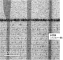
第3の原料溶液を原料溶液4aとして用いて、超音波振動子6を2.4MHzで振動させ、その振動を、水5aを通じて原料溶液4aに伝播させることによって、原料溶液4aを微粒子化させて原料微粒子4bを生成した。この原料微粒子4bが、キャリアガスによって成膜室7内に導入され、そして、大気圧下、500℃にて、成膜室7内でミストが反応して、バッファ層上に薄膜が形成された。なお、成膜時間は180分であり、膜厚は8μmであった。得られた薄膜について、X線回折装置(リガク社製、Smartlab)を用いて測定したところ、α-Ga2O3であり、回転ドメインの含有率は0%であった。なお、得られた結晶性酸化物半導体膜のTEM像を図4に示し、バッファ層のTEM像を図5に示す。また、XRDデータを図6に示す。
5. Formation of Crystallized Oxide Semiconductor Film Using the third raw material solution as the
(比較例1)
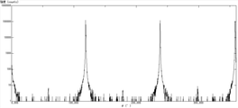
原料溶液として下記の比較例用原料溶液を用いて、成膜温度を600℃とし、成膜時間を60分としたこと以外は、上記5.と同様にして成膜することによりバッファ層を形成した。バッファ層の形成後、上記5.と同様にして、バッファ層上に成膜することにより、α-Ga2O3膜を形成した。相の同定は、X線回折装置を用いた。XRDデータを図7に示す。
(Comparative Example 1)
The above 5. The above 5. The buffer layer was formed by forming a film in the same manner as in the above. After forming the buffer layer, the above 5. In the same manner as above, an α-Ga 2 O 3 film was formed by forming a film on the buffer layer. An X-ray diffractometer was used to identify the phase. The XRD data is shown in FIG.
(比較例1用原料溶液)
アルミニウムアセチルアセトナート14mol/Lに対し、ガリウムアセチルアセトナート2mol/Lの割合となるように水溶液を調整し、この際、さらに塩酸を体積比で2%となるように含有させ、これを比較例用原料溶液とした。
(Raw material solution for Comparative Example 1)
The aqueous solution was adjusted so that the ratio of gallium acetylacetonate was 2 mol / L to 14 mol / L of aluminum acetylacetonate, and at this time, hydrochloric acid was further contained so as to be 2% by volume, and this was used as a comparative example. It was used as a raw material solution.
(比較例2)
バッファ層を形成しなかったこと以外、上記実施例と同様にしてα-Ga2O3膜を形成した。XRDデータを図8に示す。
(Comparative Example 2)
The α-Ga 2 O 3 film was formed in the same manner as in the above embodiment except that the buffer layer was not formed. The XRD data is shown in FIG.
6.評価
上記5.で得られた結晶性酸化物半導体膜および比較例で得られたα-Ga2O3膜について、各物性を評価した。結果を下記表1に示す。なお、反りは、5mm間の両端の点を通る最短の直線と、凹または凸の頂点との最短の距離を測定した。また、表1中、「1010異相ピークの有無」は、1 0 10面の逆格子マッピングを測定し、基板と膜以外のピークの有無を確認した。また、回転ドメインの含有率等は、X線回折装置(リガク社製、Smartlab)を用いて測定した。なお、測定の条件は次の通りである。
6. Evaluation Above 5. The physical characteristics of the crystalline oxide semiconductor film obtained in 1 and the α-Ga 2 O 3 film obtained in Comparative Example were evaluated. The results are shown in Table 1 below. For the warp, the shortest distance between the shortest straight line passing through the points at both ends between 5 mm and the concave or convex apex was measured. In addition, in Table 1, “presence / absence of 1010 heterogeneous peaks” was measured by measuring the reciprocal lattice mapping of 1010 planes, and the presence / absence of peaks other than the substrate and the membrane was confirmed. In addition, the content of the rotating domain and the like were measured using an X-ray diffractometer (Smartlab manufactured by Rigaku Co., Ltd.). The measurement conditions are as follows.
(X線測定条件)
104面Φスキャンを実施
XG_CURRENT 200mA
XG_VOLTAGE 45kV
X線源 CuKα1
検出器 モノクロメータ SC-70
SCAN_SPEED 200 deg/min
SCAN_STEP 0.200 deg
Φスキャン 0~360deg
CBO選択スリット PB
入射光学素子 Ge(220)x2
入射平行スリット Soller_slit_open
長手制限スリット 5.0mm
受光平行スリット Soller_slit_5.0deg
受光光学素子 PSA_open
受光平行スリット Soller_slit_5.0deg
HV 660V
PHA 561.25mV
(X-ray measurement conditions)
Performed 104-sided Φ scan
XG_CURRENT 200mA
XG_VOLTAGE 45kV
X-ray source CuKα1
Detector Monochromator SC-70
SCAN_SPEED 200 deg / min
SCAN_STEP 0.200 deg
Φ scan 0-360deg
CBO selection slit PB
Incident optical element Ge (220) x2
Incident parallel slit Slider_slit_open
Longitudinal limiting slit 5.0 mm
Light receiving parallel slit Slider_slit_5.0deg
Light receiving optical element PSA_open
Light receiving parallel slit Slider_slit_5.0deg
HV 660V
PHA 561.25mV

表1の結果から、実施例のα-Ga2O3膜は、回転ドメインがなく、結晶性等の成膜品質に優れており、反りも低減されていることがわかる。 From the results in Table 1, it can be seen that the α-Ga 2 O 3 film of the example has no rotation domain, is excellent in film formation quality such as crystallinity, and has reduced warpage.
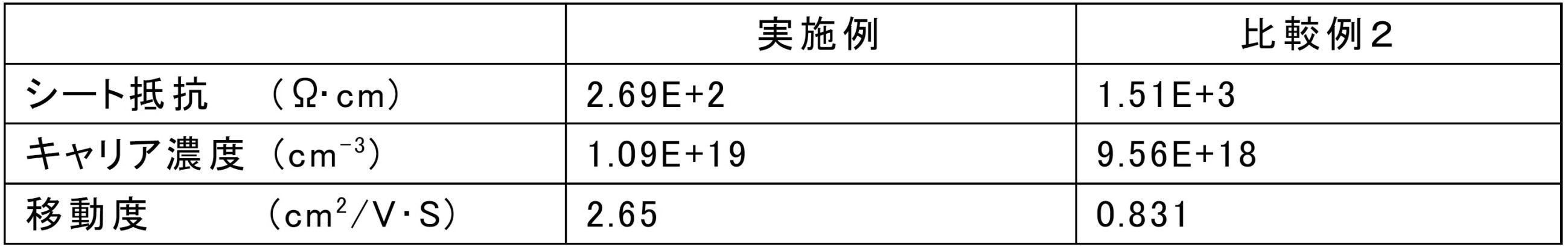
また、実施例および比較例2のα-Ga2O3膜につき、ホール効果測定を実施した。結果を下記表2に示す。表2の結果から、本発明の結晶性酸化物半導体膜は、電気特性も優れていることがわかる。 In addition, Hall effect measurements were performed on the α - Ga 2 O3 films of Examples and Comparative Examples 2. The results are shown in Table 2 below. From the results in Table 2, it can be seen that the crystalline oxide semiconductor film of the present invention is also excellent in electrical characteristics.
本発明の結晶性酸化物半導体膜は、半導体(例えば化合物半導体電子デバイス等)、電子部品・電気機器部品、光学・電子写真関連装置、工業部材などあらゆる分野に用いることができるが、特に、半導体装置に有用である。 The crystalline oxide semiconductor film of the present invention can be used in all fields such as semiconductors (for example, compound semiconductor electronic devices, etc.), electronic parts / electrical equipment parts, optical / electrophotographic-related equipment, industrial parts, etc., but in particular, semiconductors. Useful for equipment.
1 成膜装置
2a キャリアガス源
2b キャリアガス(希釈)源
3a 流量調節弁
3b 流量調節弁
4 ミスト発生源
4a 原料溶液
4b 原料微粒子
5 容器
5a 水
6 超音波振動子
6a 電極
6b 圧電体素子
6c 電極
6d 弾性体
6e 支持体
7 成膜室
8 ホットプレート
9 供給管
10 基板
16 発振器
1
Claims (10)
Priority Applications (1)
| Application Number | Priority Date | Filing Date | Title |
|---|---|---|---|
| JP2019226565A JP7016489B2 (en) | 2019-12-16 | 2019-12-16 | Crystalline oxide semiconductor film, semiconductor device |
Applications Claiming Priority (1)
| Application Number | Priority Date | Filing Date | Title |
|---|---|---|---|
| JP2019226565A JP7016489B2 (en) | 2019-12-16 | 2019-12-16 | Crystalline oxide semiconductor film, semiconductor device |
Related Parent Applications (1)
| Application Number | Title | Priority Date | Filing Date |
|---|---|---|---|
| JP2015035938A Division JP6876895B2 (en) | 2015-02-25 | 2015-02-25 | Crystalline oxide semiconductor film, semiconductor device |
Publications (2)
| Publication Number | Publication Date |
|---|---|
| JP2020057805A JP2020057805A (en) | 2020-04-09 |
| JP7016489B2 true JP7016489B2 (en) | 2022-02-07 |
Family
ID=70107737
Family Applications (1)
| Application Number | Title | Priority Date | Filing Date |
|---|---|---|---|
| JP2019226565A Active JP7016489B2 (en) | 2019-12-16 | 2019-12-16 | Crystalline oxide semiconductor film, semiconductor device |
Country Status (1)
| Country | Link |
|---|---|
| JP (1) | JP7016489B2 (en) |
Citations (4)
| Publication number | Priority date | Publication date | Assignee | Title |
|---|---|---|---|---|
| JP2013021124A (en) | 2011-07-11 | 2013-01-31 | Dowa Electronics Materials Co Ltd | Group iii nitride epitaxial substrate and manufacturing method thereof |
| WO2013035843A1 (en) | 2011-09-08 | 2013-03-14 | 株式会社タムラ製作所 | Ga2O3 SEMICONDUCTOR ELEMENT |
| JP2014072517A (en) | 2013-06-21 | 2014-04-21 | Roca Kk | Semiconductor device and manufacturing method of the same, and crystal and manufacturing method of the same |
| JP2014072463A (en) | 2012-09-28 | 2014-04-21 | Roca Kk | Semiconductor device and crystal |
-
2019
- 2019-12-16 JP JP2019226565A patent/JP7016489B2/en active Active
Patent Citations (4)
| Publication number | Priority date | Publication date | Assignee | Title |
|---|---|---|---|---|
| JP2013021124A (en) | 2011-07-11 | 2013-01-31 | Dowa Electronics Materials Co Ltd | Group iii nitride epitaxial substrate and manufacturing method thereof |
| WO2013035843A1 (en) | 2011-09-08 | 2013-03-14 | 株式会社タムラ製作所 | Ga2O3 SEMICONDUCTOR ELEMENT |
| JP2014072463A (en) | 2012-09-28 | 2014-04-21 | Roca Kk | Semiconductor device and crystal |
| JP2014072517A (en) | 2013-06-21 | 2014-04-21 | Roca Kk | Semiconductor device and manufacturing method of the same, and crystal and manufacturing method of the same |
Non-Patent Citations (3)
| Title |
|---|
| Kazuaki Akaiwa and Shizuo Fujita,Electrical Conductive Corundum-Structured α-Ga2O3 Thin Films on Sapphire with Tin-Doping Grown by S,Japanese Journal of Applied Physics,2012年06月14日,51,070203 |
| Raveen Kumaran et al.,Epitaxial Nd-doped α-(Al1-xGax)2O3 films on sapphire for solid-state waveguide lasers,Optics Letters,Vol. 35, No. 22,米国,Optical Society of America,2010年11月15日,pp. 3793-3795 |
| 金子健太郎,コランダム構造酸化ガリウム系混晶薄膜の成長と物性(Dissertation_全文),京都大学博士論文,日本,京都大学,2014年01月31日,第50~54、60頁 |
Also Published As
| Publication number | Publication date |
|---|---|
| JP2020057805A (en) | 2020-04-09 |
Similar Documents
| Publication | Publication Date | Title |
|---|---|---|
| JP6876895B2 (en) | Crystalline oxide semiconductor film, semiconductor device | |
| JP2016100592A (en) | Crystalline laminate structure and method for manufacturing the same | |
| JP7404594B2 (en) | Semiconductor devices and semiconductor systems including semiconductor devices | |
| JP6701472B2 (en) | Crystalline oxide semiconductor film and semiconductor device | |
| JP6945121B2 (en) | Crystalline semiconductor membranes and semiconductor devices | |
| JP7457366B2 (en) | Semiconductor devices and semiconductor systems including semiconductor devices | |
| JP2018060992A (en) | Semiconductor device | |
| JP2019163200A (en) | Method of manufacturing crystal film | |
| JP7016489B2 (en) | Crystalline oxide semiconductor film, semiconductor device | |
| JP6533982B2 (en) | Quantum well structure, laminated structure and semiconductor device | |
| JP2017005147A (en) | Crystalline semiconductor film, lamination structure, and semiconductor device | |
| JP2016157879A (en) | Crystalline oxide semiconductor film and semiconductor device | |
| TWI804527B (en) | Semiconductor device and semiconductor system | |
| JP6980183B2 (en) | Crystalline oxide semiconductor film, semiconductor device | |
| WO2020004250A1 (en) | Crystalline oxide film | |
| JPWO2020004249A1 (en) | Film formation method and crystalline laminated structure | |
| JPWO2020013260A1 (en) | Semiconductor devices and semiconductor systems including semiconductor devices | |
| JP2017010966A (en) | Crystalline semiconductor film, laminate structure and semiconductor device | |
| JPWO2020013261A1 (en) | Laminated structures, semiconductor devices and semiconductor systems including laminated structures | |
| JP2017010967A (en) | Deposition method | |
| JPWO2019098296A1 (en) | Semiconductor device | |
| WO2023149180A1 (en) | Crystalline oxide film, multilayer structure, semiconductor device, and method for producing crystalline oxide film | |
| JP6770674B2 (en) | Laminated structures and semiconductor devices | |
| JP2023156732A (en) | Crystalline laminated structure, semiconductor device and method for manufacturing crystalline laminated structure | |
| JP6774593B2 (en) | Crystalline oxide film |
Legal Events
| Date | Code | Title | Description |
|---|---|---|---|
| A621 | Written request for application examination |
Free format text: JAPANESE INTERMEDIATE CODE: A621 Effective date: 20191226 |
|
| A977 | Report on retrieval |
Free format text: JAPANESE INTERMEDIATE CODE: A971007 Effective date: 20201130 |
|
| A131 | Notification of reasons for refusal |
Free format text: JAPANESE INTERMEDIATE CODE: A131 Effective date: 20201215 |
|
| A601 | Written request for extension of time |
Free format text: JAPANESE INTERMEDIATE CODE: A601 Effective date: 20210215 |
|
| A521 | Request for written amendment filed |
Free format text: JAPANESE INTERMEDIATE CODE: A523 Effective date: 20210413 |
|
| A521 | Request for written amendment filed |
Free format text: JAPANESE INTERMEDIATE CODE: A523 Effective date: 20210428 |
|
| A02 | Decision of refusal |
Free format text: JAPANESE INTERMEDIATE CODE: A02 Effective date: 20210622 |
|
| A521 | Request for written amendment filed |
Free format text: JAPANESE INTERMEDIATE CODE: A523 Effective date: 20210917 |
|
| C60 | Trial request (containing other claim documents, opposition documents) |
Free format text: JAPANESE INTERMEDIATE CODE: C60 Effective date: 20210917 |
|
| C11 | Written invitation by the commissioner to file amendments |
Free format text: JAPANESE INTERMEDIATE CODE: C11 Effective date: 20211026 |
|
| A911 | Transfer to examiner for re-examination before appeal (zenchi) |
Free format text: JAPANESE INTERMEDIATE CODE: A911 Effective date: 20211122 |
|
| C21 | Notice of transfer of a case for reconsideration by examiners before appeal proceedings |
Free format text: JAPANESE INTERMEDIATE CODE: C21 Effective date: 20211124 |
|
| TRDD | Decision of grant or rejection written | ||
| A01 | Written decision to grant a patent or to grant a registration (utility model) |
Free format text: JAPANESE INTERMEDIATE CODE: A01 Effective date: 20211214 |
|
| A61 | First payment of annual fees (during grant procedure) |
Free format text: JAPANESE INTERMEDIATE CODE: A61 Effective date: 20220112 |