EP4472382A1 - Display panel and display device - Google Patents
Display panel and display device Download PDFInfo
- Publication number
- EP4472382A1 EP4472382A1 EP22923209.5A EP22923209A EP4472382A1 EP 4472382 A1 EP4472382 A1 EP 4472382A1 EP 22923209 A EP22923209 A EP 22923209A EP 4472382 A1 EP4472382 A1 EP 4472382A1
- Authority
- EP
- European Patent Office
- Prior art keywords
- sub
- circuits
- pixels
- display area
- pixel
- Prior art date
- Legal status (The legal status is an assumption and is not a legal conclusion. Google has not performed a legal analysis and makes no representation as to the accuracy of the status listed.)
- Pending
Links
Images








Classifications
-
- H—ELECTRICITY
- H10—SEMICONDUCTOR DEVICES; ELECTRIC SOLID-STATE DEVICES NOT OTHERWISE PROVIDED FOR
- H10K—ORGANIC ELECTRIC SOLID-STATE DEVICES
- H10K59/00—Integrated devices, or assemblies of multiple devices, comprising at least one organic light-emitting element covered by group H10K50/00
- H10K59/10—OLED displays
- H10K59/12—Active-matrix OLED [AMOLED] displays
- H10K59/121—Active-matrix OLED [AMOLED] displays characterised by the geometry or disposition of pixel elements
-
- G—PHYSICS
- G09—EDUCATION; CRYPTOGRAPHY; DISPLAY; ADVERTISING; SEALS
- G09G—ARRANGEMENTS OR CIRCUITS FOR CONTROL OF INDICATING DEVICES USING STATIC MEANS TO PRESENT VARIABLE INFORMATION
- G09G3/00—Control arrangements or circuits, of interest only in connection with visual indicators other than cathode-ray tubes
- G09G3/20—Control arrangements or circuits, of interest only in connection with visual indicators other than cathode-ray tubes for presentation of an assembly of a number of characters, e.g. a page, by composing the assembly by combination of individual elements arranged in a matrix no fixed position being assigned to or needed to be assigned to the individual characters or partial characters
- G09G3/22—Control arrangements or circuits, of interest only in connection with visual indicators other than cathode-ray tubes for presentation of an assembly of a number of characters, e.g. a page, by composing the assembly by combination of individual elements arranged in a matrix no fixed position being assigned to or needed to be assigned to the individual characters or partial characters using controlled light sources
- G09G3/30—Control arrangements or circuits, of interest only in connection with visual indicators other than cathode-ray tubes for presentation of an assembly of a number of characters, e.g. a page, by composing the assembly by combination of individual elements arranged in a matrix no fixed position being assigned to or needed to be assigned to the individual characters or partial characters using controlled light sources using electroluminescent panels
- G09G3/32—Control arrangements or circuits, of interest only in connection with visual indicators other than cathode-ray tubes for presentation of an assembly of a number of characters, e.g. a page, by composing the assembly by combination of individual elements arranged in a matrix no fixed position being assigned to or needed to be assigned to the individual characters or partial characters using controlled light sources using electroluminescent panels semiconductive, e.g. using light-emitting diodes [LED]
- G09G3/3208—Control arrangements or circuits, of interest only in connection with visual indicators other than cathode-ray tubes for presentation of an assembly of a number of characters, e.g. a page, by composing the assembly by combination of individual elements arranged in a matrix no fixed position being assigned to or needed to be assigned to the individual characters or partial characters using controlled light sources using electroluminescent panels semiconductive, e.g. using light-emitting diodes [LED] organic, e.g. using organic light-emitting diodes [OLED]
- G09G3/3225—Control arrangements or circuits, of interest only in connection with visual indicators other than cathode-ray tubes for presentation of an assembly of a number of characters, e.g. a page, by composing the assembly by combination of individual elements arranged in a matrix no fixed position being assigned to or needed to be assigned to the individual characters or partial characters using controlled light sources using electroluminescent panels semiconductive, e.g. using light-emitting diodes [LED] organic, e.g. using organic light-emitting diodes [OLED] using an active matrix
- G09G3/3233—Control arrangements or circuits, of interest only in connection with visual indicators other than cathode-ray tubes for presentation of an assembly of a number of characters, e.g. a page, by composing the assembly by combination of individual elements arranged in a matrix no fixed position being assigned to or needed to be assigned to the individual characters or partial characters using controlled light sources using electroluminescent panels semiconductive, e.g. using light-emitting diodes [LED] organic, e.g. using organic light-emitting diodes [OLED] using an active matrix with pixel circuitry controlling the current through the light-emitting element
-
- H—ELECTRICITY
- H10—SEMICONDUCTOR DEVICES; ELECTRIC SOLID-STATE DEVICES NOT OTHERWISE PROVIDED FOR
- H10K—ORGANIC ELECTRIC SOLID-STATE DEVICES
- H10K59/00—Integrated devices, or assemblies of multiple devices, comprising at least one organic light-emitting element covered by group H10K50/00
- H10K59/10—OLED displays
- H10K59/12—Active-matrix OLED [AMOLED] displays
- H10K59/131—Interconnections, e.g. wiring lines or terminals
-
- H—ELECTRICITY
- H10—SEMICONDUCTOR DEVICES; ELECTRIC SOLID-STATE DEVICES NOT OTHERWISE PROVIDED FOR
- H10K—ORGANIC ELECTRIC SOLID-STATE DEVICES
- H10K59/00—Integrated devices, or assemblies of multiple devices, comprising at least one organic light-emitting element covered by group H10K50/00
- H10K59/30—Devices specially adapted for multicolour light emission
- H10K59/35—Devices specially adapted for multicolour light emission comprising red-green-blue [RGB] subpixels
- H10K59/353—Devices specially adapted for multicolour light emission comprising red-green-blue [RGB] subpixels characterised by the geometrical arrangement of the RGB subpixels
-
- G—PHYSICS
- G09—EDUCATION; CRYPTOGRAPHY; DISPLAY; ADVERTISING; SEALS
- G09G—ARRANGEMENTS OR CIRCUITS FOR CONTROL OF INDICATING DEVICES USING STATIC MEANS TO PRESENT VARIABLE INFORMATION
- G09G2300/00—Aspects of the constitution of display devices
- G09G2300/04—Structural and physical details of display devices
- G09G2300/0404—Matrix technologies
- G09G2300/0408—Integration of the drivers onto the display substrate
-
- G—PHYSICS
- G09—EDUCATION; CRYPTOGRAPHY; DISPLAY; ADVERTISING; SEALS
- G09G—ARRANGEMENTS OR CIRCUITS FOR CONTROL OF INDICATING DEVICES USING STATIC MEANS TO PRESENT VARIABLE INFORMATION
- G09G2300/00—Aspects of the constitution of display devices
- G09G2300/04—Structural and physical details of display devices
- G09G2300/0421—Structural details of the set of electrodes
- G09G2300/0426—Layout of electrodes and connections
-
- G—PHYSICS
- G09—EDUCATION; CRYPTOGRAPHY; DISPLAY; ADVERTISING; SEALS
- G09G—ARRANGEMENTS OR CIRCUITS FOR CONTROL OF INDICATING DEVICES USING STATIC MEANS TO PRESENT VARIABLE INFORMATION
- G09G2300/00—Aspects of the constitution of display devices
- G09G2300/04—Structural and physical details of display devices
- G09G2300/0439—Pixel structures
- G09G2300/0465—Improved aperture ratio, e.g. by size reduction of the pixel circuit, e.g. for improving the pixel density or the maximum displayable luminance or brightness
-
- G—PHYSICS
- G09—EDUCATION; CRYPTOGRAPHY; DISPLAY; ADVERTISING; SEALS
- G09G—ARRANGEMENTS OR CIRCUITS FOR CONTROL OF INDICATING DEVICES USING STATIC MEANS TO PRESENT VARIABLE INFORMATION
- G09G2300/00—Aspects of the constitution of display devices
- G09G2300/08—Active matrix structure, i.e. with use of active elements, inclusive of non-linear two terminal elements, in the pixels together with light emitting or modulating elements
- G09G2300/0804—Sub-multiplexed active matrix panel, i.e. wherein one active driving circuit is used at pixel level for multiple image producing elements
-
- H—ELECTRICITY
- H10—SEMICONDUCTOR DEVICES; ELECTRIC SOLID-STATE DEVICES NOT OTHERWISE PROVIDED FOR
- H10K—ORGANIC ELECTRIC SOLID-STATE DEVICES
- H10K59/00—Integrated devices, or assemblies of multiple devices, comprising at least one organic light-emitting element covered by group H10K50/00
- H10K59/60—OLEDs integrated with inorganic light-sensitive elements, e.g. with inorganic solar cells or inorganic photodiodes
- H10K59/65—OLEDs integrated with inorganic image sensors
Definitions
- the present application relates to the field of display, and particularly to a display panel and a display apparatus.
- sub-pixels may be arranged in a photosensitive area where a photosensitive component such as a camera is located, and pixel circuits corresponding to the sub-pixels may be arranged at other positions in a display area.
- pixel circuits originally close to a frame display area will be placed at other positions. All the above results in non-uniform arrangement density of the pixel circuits in the display area, which causes display difference in the display panel.
- Embodiments of the present application provide a display panel and a display apparatus, which are intended to improve the display effect of the display panel.
- Embodiments of a first aspect of the present application provide a display panel including a first display area and a second display area, the display panel including: a plurality of pixel blocks including a plurality of sub-pixels, each of the pixel blocks including a sub-pixels of the plurality of sub-pixels, the plurality of sub-pixels including a plurality of first sub-pixels located in the first display area and a plurality of second sub-pixels located in the second display area; and a plurality of circuit blocks located in the second display area, each of the circuit blocks including b pixel circuits, the b pixel circuits including first circuits and second circuits, at least part of the first circuits being configured to drive the first sub-pixels, and the second circuits being configured to drive the second sub-pixels; herein both a and b are positive integers greater than 0, and a is less than b , in the second display area, an orthographic projection of the circuit block in a thickness direction of the display panel is located within an orthographic
- Embodiments of a second aspect of the present application provide a display apparatus including the display panel according to the embodiments of the first aspect.
- the circuit blocks are located in the second display area, that is, the pixel circuits for driving the first sub-pixels and the second sub-pixels are all located in the second display area, so that the light transmittance of the first display area can be greater than the light transmittance of the second display area.
- Photosensitive components may be integrated at the back of the first display area of the display panel to achieve under-screen integration for the photosensitive components such as a camera.
- driving circuits such as a shift register of the display panel may be arranged in the first display area to achieve a narrow frame design for the display panel.
- the circuit blocks are located in the second display area, each of the circuit blocks includes b pixel circuits, the pixel block in the second display area includes a second sub-pixels, and b is greater than a , so that the spare first circuits in at least part of the circuit blocks can be used to drive the first sub-pixels in the first display area.
- An orthographic projection of the circuit block in a thickness direction of the display panel is located within an orthographic projection of the pixel block in the thickness direction.
- the arrangement of the circuit blocks is the same as the arrangement of the pixel blocks, the arrangement of the circuit blocks is more uniform, the display effect of the second display area is improved, and further the display effect of the display panel is improved.
- the distance between the second circuit in at least part of the circuit blocks and the second sub-pixel driven by the second circuit can be reduced, the length of the wrings between at least part of the second circuits and the second sub-pixels can be reduced, and the signal transmission stability is guaranteed.
- photosensitive components such as a front camera, an infrared light sensor, and a proximity light sensor need to be integrated at a side of the display panel.
- a light-transmitting display area may be arranged on the electronic device and the photosensitive components may be arranged at the back of the light-transmitting display area, so that a full-screen display can be achieved for the electronic device while ensuring that the photosensitive components operate normally.
- the driving circuits for the light-transmitting area are usually arranged in a non-light-transmitting area, which causes non-uniform display in the non-light-transmitting area of the display panel.
- the embodiments of the present application provide a display panel 100, which may be an organic light emitting diode (OLED) display panel 100.
- a display panel 100 which may be an organic light emitting diode (OLED) display panel 100.
- OLED organic light emitting diode
- FIG. 1 shows a schematic top view of a display panel 100 according to the embodiments of the present application
- Fig. 2 shows a partial enlarged schematic structural diagram of area Q in Fig. 1
- Fig. 3 shows a partial enlarged schematic structural diagram of area Q in Fig. 1 in another example.
- Fig. 2 and Fig. 3 illustrate different layer structures.
- Fig. 2 illustrates an arrangement structure diagram of sub-pixels 110a in Q in Fig. 1
- Fig. 3 differs from Fig. 2 in that Fig. 3 illustrates an arrangement structure diagram of pixel circuits 120a in a second display area AA2 in Q, and further illustrates a schematic arrangement structure diagram of the sub-pixels 110a in a first display area AA1.
- the embodiments of the first aspect of the present application provide a display panel 100 including the first display area AA1 and the second display area AA2, and the display panel 100 includes: a plurality of sub-pixels including a plurality of first sub-pixels 111 located in the first display area AA1 and a plurality of second sub-pixels 112 located in the second display area AA2; a plurality of pixel blocks 110 including the plurality of sub-pixels, each of the pixel blocks 110 including a sub-pixels 110a of the plurality of sub-pixels, the plurality of sub-pixels 110a including a plurality of first sub-pixels 111 located in the first display area AA1 and a plurality of second sub-pixels 112 located in the second display area AA2; and a plurality of circuit blocks 120 located in the second display area AA2, each of the circuit blocks 120 including b pixel circuits 120a, the b pixel circuits 120a including first circuits
- the structures of the pixel block 110 and the circuit block 120 are defined by rectangular boxes in Fig. 2 and Fig. 3 , but the structure of the display panel 100 in the present application is not limited by the rectangular boxes.
- the rectangular box includes a small portion of a sub-pixel 110a which does not belong to a same pixel block 110, and a sub-pixel 100a with an area within the rectangular box greater than 50% of a total area of the sub-pixel 100a is the sub-pixel 110a within the pixel block 110 represented by the rectangular box.
- All of the a sub-pixels 110a in each pixel block 110 located in the first display area AA1 are the first sub-pixels 111, and all of the a sub-pixel 110a in each pixel block 110 located in the second display area AA2 are the second sub-pixel 112.
- the circuit blocks 120 are located in the second display area AA2, that is, the pixel circuits 120a for driving the first sub-pixels 111 and the second sub-pixels 112 are all located in the second display area AA2, so that the light transmittance of the first display area AA1 can be greater than the light transmittance of the second display area AA2.
- Photosensitive components may be integrated at the back of the first display area AA1 of the display panel 100 to achieve under-screen integration for the photosensitive components such as cameras.
- driving circuits such as a shift register of the display panel 100 may be arranged in the first display area AA1 to achieve a narrow frame design for the display panel 100.
- the circuit blocks 120 are located in the second display area AA2, each of the circuit blocks 120 includes b pixel circuits 120a, the pixel block 110 includes a second sub-pixels 112 located in the second display area AA2, b is greater than a, a second circuits 122 are arranged in the circuit block 120 so as to drive the a second sub-pixels 112 in the pixel block 110, ( b-a ) first circuits 120 may be arranged in the circuit block 120, and at least part of the first circuits 121 in the circuit block 120 can be used to drive the first sub-pixels 111 in the first display area AA1.
- An orthographic projection of the circuit block 120 in a thickness direction of the display panel 100 is located within an orthographic projection of the pixel block 110 in the thickness direction.
- the arrangement of a plurality of second circuits 122 in the circuit block 120 is the same as the arrangement of a plurality of second sub-pixels 112 in the pixel block 110, the arrangement of the circuit blocks 120 is more uniform, and the display effect of the second display area AA2 is improved.
- the distance between the second circuit 122 in at least part of the circuit blocks 120 and the second sub-pixel 112 driven by the second circuit 122 can be reduced, the length of the wirings between at least part of the second circuits 122 and the second sub-pixels 112 can be reduced, and the signal transmission stability is guaranteed.
- the pixel block 110 in the second display area AA2 includes a second sub-pixels 112 and the pixel block 110 in the first display area AA1 includes a first sub-pixels 111. If a part of display area is located between the first display area AA1 and the second display area AA2, the pixel block 110 between the first display area AA1 and the second display area AA2 may further include the first sub-pixels 111 and the second sub-pixel 112, and a sum of the number of the first sub-pixels 111 and the number of the second sub-pixels 112 is a.
- the circuit block 120 may include b first circuits 121 or b second circuits 122.
- the pixel circuit 120a may include both the first circuit 121 and the second circuit 122, and a sum of the number of the first circuits 121 and the number of the second circuits 122 is b.
- an area of the orthographic projection of the pixel block 110 in the thickness direction overlaps the orthographic projection of the circuit block 120 in the thickness direction, so that the area of the pixel circuits 120a in the pixel block 110 is relatively great.
- a distribution area of the first circuit 121 is equal to a distribution area of the second circuit 122, so that the display effect of the second display area AA2 can be further improved, and display difference due to different distribution areas of the first circuit 121 and the second circuit 122 can be avoided.
- a circuit structure of the first circuit 121 is the same as a circuit structure of the second circuit 122, but the first circuit 121 is configured to drive the first sub-pixel 111, while the second circuit 122 is configured to drive the second sub-pixel 112.
- the orthographic projection of the circuit block 120 in the thickness direction of the display panel 100 is the orthographic projection of the circuit block 120 on a display surface of the display panel 100.
- the orthographic projection of the pixel block 110 in the thickness direction is the orthographic projection of the pixel block 110 on the display surface of the display panel 100.
- the orthographic projection of the pixel block 110 in the thickness direction of the display panel 100 is an area where the orthographic projections of the a sub-pixels 110a in the pixel block 110 in the thickness direction of the display panel 100 are located.
- the area where the pixel block 110 is located is the arrangement area occupied by the a sub-pixels 110a in the pixel arrangement structure.
- the arrangement size of a single sub-pixel 110a is 1cm ⁇ 1cm, that is, the size of the orthographic projection of a single sub-pixel 110a in the thickness direction of the display panel 100 is 1cm ⁇ 1cm, and the area where the pixel block 110 is located is an area formed by a areas of 1cm ⁇ 1cm. This is merely for illustration and does not mean that the actual arrangement size of the sub-pixel 110a is 1cm ⁇ 1cm.
- the a sub-pixels 110a in the pixel block 110 are arranged adjacently. For example, as shown in Fig. 2 and Fig. 3 , if a is equal to 16 and the pixel block 110 includes 16 sub-pixels 110a, the 16 sub-pixels 110a in pixel block 110 are arranged adjacently. The 16 sub-pixels 110a may be located in a same row or two or more adjacent rows.
- the area where the orthographic projection of the a sub-pixels 110a in the thickness direction of the display panel 100 is located is of an average arrangement size of the a sub-pixels 110a.
- the row direction may be a first direction X
- the column direction may be a second direction Y
- the row direction may be the second direction Y
- the column direction may be the first direction X.
- the sub-pixels 110a of the display panel 100 are arranged to form a pixel arrangement structure which includes a plurality of repeating units, the repeating unit includes a plurality of sub-pixels 110a, and the repeating units are arranged repeatedly in the row direction and the column direction to form the pixel arrangement structure.
- the number of the sub-pixels 110a included in the pixel block 110 may be related to the number of the sub-pixels 110a included in the repeating unit, for example, the number of the sub-pixels 110a included in the pixel block 110 is an integral multiple of the number of the sub-pixels 110a included in the repeating unit. For example, as shown in Fig.
- the pixel block 110 includes sixteen sub-pixels 110a, the number of the sub-pixels 110a included in the pixel block 110 is four times as many as the number of the sub-pixels 110a included in the repeating unit, that is, the pixel block 110 includes four repeating units, and the orthographic projection of the pixel block 110 in the thickness direction is the arrangement size occupied by the four repeating units.
- the orthographic projection of the circuit block 120 in the thickness direction of the display panel 100 is an area where the orthographic projection of the b sub-pixels 110a in the circuit block 120 in the thickness direction is located.
- the b pixel circuits 120a in the circuit block 120 are arranged adjacently.
- the 25 pixel circuits 120a may be located in a same row or two or more rows.
- the b pixel circuits 120a in the circuit block 120 are arranged in a same row.
- the pixel circuits 120a in circuit block 120 are compressed in the row direction, so that the orthographic projection of the b pixel circuits 120a in the thickness direction is located within the orthographic projection of the a sub-pixels 110a in the thickness direction.
- the pixel block 110 includes a plurality of the sub-pixels 110a distributed in p rows and q columns, and a product of p and q is a ;
- the circuit block 120 includes a plurality of the pixel circuits 120a distributed in e rows and f columns, and a product of e and f is b , in which p , q , e and f are all positive integers greater than 1, e ⁇ p and f ⁇ q.
- p , q , e and f are all positive integers greater than 1, and thus the pixel block 110 includes the sub-pixels 110a arranged in a plurality of rows and a plurality of columns, and the circuit block 120 includes the pixel circuits 120a arranged in a plurality of rows and a plurality of columns, so that the pixel circuits 120a are compressed in both the row direction and the column direction, thereby avoiding the technical difficulty due to the compression of the pixel circuits 120a in a same direction.
- P , q , e and f may be set in a variety of ways, and in some optional embodiments, p is equal to q , e is equal to f , and e is greater than p. That is, the pixel block 110 includes p rows and p columns of the sub-pixels 1 10a, and the circuit block 120 includes e rows and e columns of the pixel circuits 120a, so that the plurality of sub-pixels 110a in the pixel block 110 are arranged more regularly and the plurality of pixel circuits 120a in the circuit block 120 are arranged more regularly, and the size of the pixel circuits 120a can be adjusted more easily.
- the pixel block 110 includes 4 rows and 4 columns of the sub-pixels 110a.
- the circuit block 120 includes 5 rows and 5 columns of the pixel circuits 120a.
- the display panel 100 in the second display area AA2, five rows and five columns of the pixel circuits 120 are arranged in an area where four rows and four columns of the sub-pixels 110a are located.
- the number of the pixel circuits 120a arranged in the area where the four rows and four columns of the sub-pixels 110a are located is greater than the number of the sub-pixels 110a, and at least part of one row and one column of the pixel circuits 120a that are spare in the area where the four rows and four columns of the sub-pixels 110a are located may be configured to drive the first sub-pixels 111 in the first display area AA1.
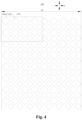
- Fig. 4 shows a schematic arrangement structure diagram of the sub-pixels 110a in W in Fig. 1
- Fig. 5 shows a schematic arrangement structure diagram of the pixel circuits 120a in W in Fig. 1 .
- the second display area AA2 includes a main display area ZA and a transition display area TA located between the main display area ZA and the first display area AA1, and at least part of the first circuits 121 located in the transition display area TA are configured to drive the first sub-pixels 111. That is, the first circuits 121 for driving the first sub-pixels 111 are located in the transition display area TA, and the first circuits 121 which are not configured to drive the first sub-pixels 111 are located in the main display area ZA.
- the first circuits 121 for driving the first sub-pixels 111 are arranged in the transition display area TA which is closer to the first display area AA1, so that the distance between the first circuit 121 and the first sub-pixel 111 which are electrically connected with each other can be reduced, the length of the connecting line between the first circuit 121 and the first sub-pixel 111 can be reduced, and the signal transmission stability is guaranteed.
- the circuit block 120 in the main display area ZA is located within the orthographic projection of the pixel block 110 driven by the circuit block 120, and the circuit block 120 in the main display area ZA includes p rows and q columns of the second circuits 122 and ( e-p ) rows and ( f-q ) columns of the first circuits 121.
- ( e-p ) rows and ( f-q ) columns of the first circuits 121 refers to the ( e-p ) rows and ( f-q ) columns from the e rows and f columns of the circuit block 120.
- each circuit block 120 in the main display area ZA includes four rows and four columns of the second circuits 122 and one row and one column of the first circuits 121, which refer to one row and one column of the first circuits 121 from the five rows and five columns of the pixel circuits 120a.
- each circuit block 120 in the main display area ZA includes 16 second circuits 122 and 9 first circuits 121.
- the number of the second circuits 122 included in the circuit block 120 in the main display area ZA is the same as the number of the second sub-pixels 112 included in the pixel block 110, so that the second circuits 122 in each circuit block 120 can be configured to drive the second sub-pixels 112 in each pixel block 110.
- the circuit block 120 in the main display area ZA is located within the orthographic projection of the pixel block 110 driven by the circuit block 120, so that the distance between the second circuit 122 and the second sub-pixel 112 driven by the second circuit 122 can be reduced, and the length of the connecting line between the second circuit 122 and the second sub-pixel 112 driven by the second circuit 122 can be reduced.
- a relative position relationship of the plurality of second circuits 122 in the circuit block 120 is the same as a relative position relationship of the plurality of second sub-pixels 112 in the pixel block 110, so that the distance between the second circuit 122 and the second sub-pixel 112 driven by the second circuit 122 can be further reduced, and the length of the connecting line between the second circuit 122 and the second sub-pixel 112 driven by the second circuit 122 can be reduced.
- the relative position relationship of the second circuits 122 in the main display area ZA and the second sub-pixels 112 driven by the second circuits 122 may be arranged in a variety of ways.
- the orthographic projection of the second circuit 122 in the thickness direction at least partially overlaps the orthographic projection of the second sub-pixel 112 driven by the second circuit 122 in the thickness direction, so that the distance between the second circuit 122 and the second sub-pixel 112 driven by the second circuit 122 can be further reduced, and the length of the connecting line between the second circuit 122 and the second sub-pixel 112 driven by the second circuit 122 can be reduced.
- the orthographic projection of the second circuit 122 in the thickness direction is staggered with the orthographic projection of the second sub-pixel 112 driven by the second circuit 122 in the thickness direction, as long as the orthographic projection in the thickness direction of the circuit block 120 where the second circuit 122 is located is located within the orthographic projection in the thickness direction of the pixel block 110 where the second sub-pixel 112 driven by the second circuit 122 is located.
- the first circuit 121 in the circuit block 120 is located at a side of the second circuit 122 in the row direction, or the first circuit 121 is located at a side of the plurality of second circuits 122 in the column direction.
- the first circuit 121 is located in the middle of the plurality of second circuits 122 in the row direction and/or column direction, so that the staggered size between the second circuit 122 and the second sub-pixel 112 driven by the second circuit 122 is reduce, and the wiring length between the second circuit 122 and the second sub-pixel 112 driven by the second circuit 122 is reduced.
- the first circuits 121 and the second circuits 122 may be arranged in a variety of ways.
- the arrangement of the first circuits 121 and the second circuits 122 in the transition display area TA is the same as the arrangement of the first circuits 121 and the second circuits 122 in the main display area ZA. That is, the circuit block 120 in the transition display area TA is located within the orthographic projection of the pixel block 110 driven by the circuit block 120, and the circuit block 120 in the transition display area TA includes p rows and q columns of the second circuits 122 and ( e-p ) rows and ( f-q ) columns of the first circuits 121.
- the display difference between the transition display area TA and the main display area ZA can be further reduced, the distance between the second circuit 122 in the transition display area TA and the second sub-pixel 112 driven by the second circuit 122 can be reduced, and the length of the connecting line between the second circuit 122 and the second sub-pixel 112 driven by the second circuit 122 can be reduced.
- a further relative position relationship of the plurality of second circuits 122 in the circuit block 120 is the same as a further relative position relationship of the plurality of second sub-pixels 112 in the pixel block 110, so that the distance between the second circuit 122 in the transition display area TA and the second sub-pixel 112 driven by the second circuit 122 is reduced, and the length of the connecting line between the second circuit 122 and the second sub-pixel 112 driven by the second circuit 122 is reduced.
- the first circuits 121 may be arranged in a variety of ways.
- the first circuits 121 include a plurality of row circuits 121a arranged side by side in a row direction and column circuits 121b arranged side by side in a column direction, and at least part of the row circuits 121a and/or the column circuits 121b are configured to drive the first sub-pixels 111.
- the row circuits 121a refer to a plurality of the first circuits 121 arranged in the row direction
- the column circuits 121b refer to a plurality of the first circuits 121 arranged in the column direction.
- the row direction and the column direction intersect, so the first circuit 121 at the intersection position may be either the row circuit 121a or the column circuit 121b.
- no second circuit 122 is arranged in the row where the row circuits 121a are located, and no second circuit 122 is arranged in the column where the column circuits 121b are located.
- the crosstalk between the connecting line between the first sub-pixel 111 and the second circuit 122 and the connecting line between the second sub-pixel 112 and the second circuit 122 can be avoided.
- the distribution pattern of the first circuits 121 is grid shaped and includes a hollow area in which a plurality of second circuits 122 are located, that is, at least two of the first circuits 121 are arranged at intervals, at least part of the second circuits 122 are located between two adjacent first circuits 121, and the first circuits 121 are arranged around the plurality of the second circuits 122. That is, in the circuit block 120, the first circuits 121 are concentrated in a same row and a same column, so that the arrangement of the plurality of second circuits 122 in the circuit block 120 is more concentrated.
- the first display area AA1 may be arranged in a variety of ways.
- the first display area AA1 includes a regularly shaped area and an irregularly shaped area located at at least one side of the regularly shaped area in the row direction, and at least part of the first sub-pixels 111 in the irregularly shaped area and at least part of the first sub-pixels 111 in the regularly shaped area are arranged in a same row.
- the irregularly shaped area may be arranged in a variety of ways. Still referring to Fig. 1 , for example, the irregularly shaped area may include a corner area RA arranged around the second display area AA2 and being bent. Under a condition that the first display area AA1 includes the corner area RA, the pixel circuit 120a corresponding to the first sub-pixel 111 in the corner area RA is located in the second display area AA2, so that driving circuits such as a shift register and driving signal lines may be further arranged in the corner area RA, the frame size of the display panel 100 can be reduced.
- driving circuits such as a shift register and driving signal lines
- the irregularly shaped area may further include a photosensitive area UDC, and the second display area AA2 is arranged around at least part of the photosensitive area UDC.
- the pixel circuit 120a corresponding to the first sub-pixel 111 in the photosensitive area UDC is located in the second display area AA2, so that the light transmittance of the photosensitive area UDC can be increased, which facilitates the under-screen integration of the photosensitive components in the photosensitive area UDC.
- the photosensitive area UDC can display images, the display area of the display panel is increased, and a full-screen design is achieved for the display apparatus.
- the first display area AA1 includes a frame display area BA arranged around the second display area AA2 and including an end frame display area BA1 located at at least one side of the second display area AA2 in a column direction and a side frame display area BA2 located at at least one side of the second display area AA2 in a row direction.
- the pixel circuit 120a corresponding to the first sub-pixel 111 in the frame display area BA is located in the second display area AA2, so that driving circuits such as a shift register and driving signal lines may be further arranged in the frame display area BA, the frame size of the display panel 100 can be reduced, and a narrow frame design or even a frame-free design can be achieved for the display panel 100.
- the regularly shaped area may include the above frame display area BA, and the regularly shaped area may further include a part of the first display area AA1 located at at least one side of the photosensitive area UDC in the row direction.
- the corner area RA may be connected between the end frame display area BA1 and the side frame display area BA2 that are adjacent.
- the first sub-pixels 111 located in different areas may be driven by different first circuits 121.
- at least part of the row circuits 121a are configured to drive the first sub-pixels 111 located in the irregularly shaped area. Therefore, the first sub-pixels 111 in a same row in the irregularly shaped area may be driven by the row circuits 121a in a same row, which can simplify the wiring between the first sub-pixels 111 and the row circuits 121a.
- the first sub-pixels 111 in the irregularly shaped area are driven by the row circuits 121a, only a row signal line for transmitting driving signals to the row circuits 121a needs be to added, and no additional column signal line is necessary, so that the number of signal lines in the second display area AA2 can be reduced.
- the first sub-pixels 111 in the photosensitive area UDC may be driven by the row circuits 121a.
- various rows of the first sub-pixels 111 in the first display area AA1 may be driven by the row circuits 121a in different rows, that is, the first sub-pixels 111 in different rows are driven by the row circuits 121a in different rows.
- a plurality of rows of the first sub-pixels 111 in the first display area AA1 may be driven by the row circuits 121a in a same row, that is, two or more rows of the first sub-pixels 111 may be driven by the row circuits 121a in a same row.
- a row signal line may be added in the transition display area TA to transmit driving signals to the row circuits 121a.
- the display panel 100 further includes first row signal lines 131 and second row signal lines 132, the first row signal lines 131 are connected with the row circuits 121a for driving the first sub-pixels 111 and configured to transmit signals to the row circuits 121a, and the second row signal lines 132 are connected with the second circuits 122 and configured to transmit signals to the second circuits 122.
- the first row signal lines 131 are added to transmit driving signals to the row circuits 121a, thereby enabling the row circuits 121a to drive the first sub-pixels 111 to display.
- Fig. 7 shows a schematic arrangement structure diagram of the sub-pixels 110a in P in Fig. 1
- Fig. 8 shows a schematic structural diagram of the pixel circuits 120a in P in Fig. 1
- the first sub-pixels 111 in the corner area RA are illustrated in Fig. 8 .
- the first sub-pixels 111 in the corner area RA may be driven by the row circuits 121a in the second display area AA2.
- a plurality of rows of the first sub-pixels 111 in the corner area RA may be driven by a plurality of rows of the row circuits 121a.
- a plurality of rows of the first sub-pixels 111 in the corner area RA may be driven by the row circuits 121a in a same row.
- the display panel 100 further includes column signal lines (not shown) extending in the column direction and configured to transmit driving signals to the first circuits 121 and/or the second circuits 122 arranged in a same column.
- first row signal lines 131 and the second row signal lines 132 may be scanning signal lines, and the column signal lines may be data signal lines.
- first row signal lines 131 and the second row signal lines 132 may be data signal lines, and the column signal lines may be scanning signal lines.
- the display panel 100 further includes a row buffer (not shown) for storing driving signals for the first sub-pixels 111 in the irregularly shaped area and transmitting driving signals to the first row signal lines 131 according to the driving signals for the first sub-pixels 111 in the irregularly shaped area.
- a row buffer (not shown) for storing driving signals for the first sub-pixels 111 in the irregularly shaped area and transmitting driving signals to the first row signal lines 131 according to the driving signals for the first sub-pixels 111 in the irregularly shaped area.
- the display panel 100 includes a pixel jump reduction (PJR) processing module, which can copy and move images.
- PTR pixel jump reduction
- PTR pixel jump reduction
- the PJR processing module is connected with a digital to analog conversion module, so as to convert the image data to an analog voltage signal through the digital to analog conversion module.
- this first sub-pixel 111 may be driven to emit light through the first circuits 121 located in the second display area AA2 according to the light emitting requirements of the display unit.
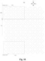
- Fig. 10 shows a schematic arrangement structure diagram of the sub-pixels 110a in I in Fig. 1
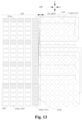
- Fig. 11 shows a schematic arrangement structure diagram of the pixel circuits 120a in I in Fig. 1 , in which the first sub-pixels 111 located in the end frame display area BA1 are also illustrated
- Fig. 12 shows a schematic arrangement structure diagram of the sub-pixels 110a in II in Fig. 1
- Fig. 13 shows a schematic arrangement structure diagram of the pixel circuits 120a in II in Fig. 1 , in which the first sub-pixels 111 located in the side frame display area BA2 are also illustrated.
- the first sub-pixels 111 in the frame display area BA are arranged in rows and columns.
- the first sub-pixels 111 in the end frame display area BA1 are arranged in a plurality of rows, and the number of the first sub-pixels 111 arranged in a same row in the end frame display area BA1 is less than or equal to the number of the row circuits 121a arranged in a same row in the transition display area TA.
- the first sub-pixels 111 in a same row in the end frame display area BA1 can be driven by the row circuits 121a arranged in a same row in the transition display area TA, and the row signal lines originally for driving the first sub-pixels 111 in a same row in the end frame display area BA1 can be moved to the transition display area TA and connected with the row circuits 121a for driving the first sub-pixels 111.
- the first sub-pixels 111 in the side frame display area BA2 are arranged in a plurality of columns, and the number of the first sub-pixels 111 arranged in a same column in the side frame display area BA2 is less than or equal to the number of the column circuits 121b arranged in a same column in the transition display area TA.
- the first sub-pixels 111 in a same column in the side frame display area BA2 can be driven by the row circuits 121a arranged in a same column in the transition display area TA, and the column signal lines originally for driving the first sub-pixels 111 in a same column in the side frame display area BA2 can be moved to the transition display area TA and connected with the column circuits 121b for driving the first sub-pixels 111.
- At least part of the row circuits 121a are configured to drive the first sub-pixels 111 located in the end frame display area BA1
- at least part of the column circuits 121b are configured to drive the first sub-pixels 111 located in the side frame display area BA2.
- No additional row signal line or column signal line is necessary, and the wiring of the signal lines of the display panel 100 can be further simplified.
- the above describes how to use the first circuits 121 in the transition display area TA to drive the first sub-pixels 111 under a condition that the arrangement of the circuit blocks 120 in the transition display area TA is the same as the arrangement of the circuit blocks 120 in the main display area ZA.
- the arrangement of the circuit blocks 120 in the transition display area TA may be different from the arrangement of the circuit blocks 120 in the main display area ZA.
- Fig. 14 shows a schematic arrangement structure diagram of pixel circuits in area I in Fig. 1 in another example.
- the first circuits 121 in the transition display area TA are all located at a side of the second circuits 122 close to the first sub-pixels 111.
- the first circuits 121 in the transition display area TA are arranged closer to the first display area AA1, which can reduce the distance between the first circuit 121 and the first sub-pixel 111 driven by the first circuit 121.
- a position relationship of the second circuit 122 for driving the second sub-pixel 112 in the transition display area TA and the first circuits 121 in the transition display area TA for driving the first sub-pixels 111 is the same as a position relationship of the second sub-pixels 112 in the transition display area TA and the first sub-pixels 111 in the first display area AA1.
- the distance between the second circuit 122 in the transition display area TA and the second sub-pixel 112 driven by the second circuit 122 and the distance between the first circuit 121 and the first sub-pixel 111 driven by the first circuit 121 can be reduced, and the intersection between the signal line for connecting the first circuit 121 and the first sub-pixel 111 and the signal line for connecting the second circuit 122 and the second sub-pixel 112 can be avoided, which simplifies the wiring of the signal lines.
- no additional row signal line or column signal line is necessary, it is only needed that the signal line for driving the first sub-pixel 111 is connected with the first circuit 121 for driving the first sub-pixel 111.
- the plurality of first circuits 121 in the transition display area TA are arranged according to the arrangement of the plurality of first sub-pixels 111 driven by the plurality of first circuits 121, and the plurality of first circuits 121 are connected with the first sub-pixels 111 in sequence, so that the lengths of a plurality of signal lines for connecting the first circuits 121 and the first sub-pixels 111 tend to be the same, and the plurality of signal lines can be prevented from intersecting with each other.
- the first display area AA1 may further include a corner area RA, a photosensitive area UDC and a side frame display area BA2, and the first circuits 121 for driving the first sub-pixels 111 in the corner area RA, the photosensitive area UDC and the side frame display area BA2 are located at a side of the second circuits 122 close to the corner area RA, the photosensitive area UDC and the side frame display area BA2.
- the first sub-pixels 111 in the corner area RA, the photosensitive area UDC and the side frame display area BA2 may also be connected with the first circuits 121 in the transition display area TA in sequence, and a relative position relationship of the first sub-pixels 111 in the corner area RA, the photosensitive area UDC and the side frame display area BA2 and the second sub-pixels 112 in the transition display area TA is the same as a relative position relationship of the first circuits 121 for driving the first sub-pixels 111 in the corner area RA, the photosensitive area UDC and the side frame display area BA2 and the second circuits 122 in the transition display area TA.
- Fig. 15 shows a cross-sectional view at C-C in Fig. 3 .
- the crosstalk between the first connection signal line 133 and other signal lines can be avoided by arranging the signal line layer 103.
- the display panel 100 further includes a substrate 101, an array base plate arranged on the substrate 101, and a pixel definition layer 102, in which the pixel circuits 120a are arranged in the array base plate.
- the pixel definition layer 102 includes a first pixel opening K1 located in the first display area AA1 and a second pixel opening K2 located in the second display area AA2.
- the first sub-pixel 111 includes a first light-emitting structure 111b located in the first pixel opening K1, a first electrode 111a located at a side of the first light-emitting structure 111b facing the array base plate, and a second electrode 111c located at a side of the first light-emitting structure 111b away from the array base plate.
- the second sub-pixel 112 includes a second light-emitting structure 121b located in the second pixel opening K2, a third electrode 121a located at a side of the second light-emitting structure 121b facing the array base plate, and a fourth electrode 121c located at a side of the second light-emitting structure 121b away from the array base plate.
- the first electrode 111a and the third electrode 121a are, for example, pixel electrodes, and the second electrode 111c and the fourth electrode 121c may be interconnected as a common electrode.
- the signal line layer 103 may be located between the array base plate and a light-emitting layer.
- the array base plate may include a first metal layer, a second metal layer and a third metal layer
- the pixel circuit 120a includes a thin film transistor (TFT), which may be a switching thin film transistor and a driving thin film transistor.
- the thin film transistor (TFT) includes a semiconductor layer, a gate, a source electrode, and a drain electrode, in which the gate may be located in the first metal layer, and the source electrode and the drain electrode may be located in the third metal layer.
- One electrode plate of a capacitor may be arranged in the second metal layer, and the other electrode plate of the capacitor may be located in the first metal layer or the third metal layer.
- the row signal line is a scanning line and may be located in the first metal layer and interconnected with the gate of the switching thin film transistor.
- the display panel 100 further includes a column signal line which is a data line and located in the third metal layer, and the column signal line may be interconnected with one of the source electrode and the drain electrode of the switching thin film transistor.
- the source electrode and the drain electrode of the driving thin film transistor of part of the first circuits 121 are connected with the first electrode 111a of the first sub-pixel 111 through the first connection signal line 133.
- At least part of the first connection signal line 133 extends in the second direction Y, and the part of the first connection signal line 133 extending in the second direction Y is located in a same film layer.
- An arrangement size of the first connection signal line 133 in the first direction X is m ⁇ m
- an arrangement size in the first direction X of the first sub-pixel 111 adjacent to the second display area AA2 along the second direction Y is n ⁇ m
- 2k first sub-pixels 111 are arranged in the second direction Y in the first display area AA1
- One of the first direction X and the second direction Y is the row direction, and the other one is the column direction. Referring to Fig. 14 , in the embodiments of the present application, for example, the first direction X is the row direction, and the second direction Y is the column direction.
- the arrangement size of the first connection signal line 133 in the first direction X includes both an extension size of the first connection signal line 133 in the first direction X and a spacing size between two first connection signal lines 133 adjacent in the first direction X.
- the arrangement size of the first sub-pixel 111 in the first direction X is an average arrangement size of the first sub-pixel 111 in the first direction X. For example, i first sub-pixels 111 are arranged in the first direction X, and the size occupied by the i first sub-pixels 111 in the first direction X is j , then the arrangement size n of the first sub-pixels 111 is equal to j / i.
- the first sub-pixel 111 adjacent to the second display area AA2 in the second direction Y is an adjoining first sub-pixel 111'.
- the first display area AA1 includes the end frame display area BA1
- two end frame display areas BA1 are respectively arranged at two sides of the second display area AA2
- k first sub-pixels 111 are arranged in the second direction Y in one end frame display area BA1.
- the extension size of the end frame display area BA1 in the second direction Y is less than or equal to the arrangement size of the k first sub-pixels 111 in the second direction Y
- the first direction X is the column direction
- the second direction Y is the row direction
- two side frame display areas BA2 are respectively arranged at two sides of the second display area AA2.
- k first sub-pixels 111 are arranged in the first direction X in one side frame display area BA2, and the extension size of the side frame display area BA2 in the first direction X is less than or equal to the arrangement size of the k first sub-pixels 111 in the first direction X.
- the radius of the photosensitive area UDC is less than or equal to the arrangement size of the k first sub-pixels 111 in the row direction.
- the arrangement size of the first connection signal line 133 in the column direction is 5 ⁇ m
- the arrangement size of the adjoining first sub-pixel 111' in the column direction is 61.7 ⁇ m
- the number of the first connection signal lines 133 that can be arranged on the adjoining first sub-pixel 111' is 11 at most
- the extension size of the first display area AA1 in the row direction is less than or equal to the arrangement size of the 11 first sub-pixels 111 in the row direction.
- the first connection signal line 133 includes a first segment 133a and a second segment 133b extending along different directions and located in different film layers, so as to reduce the risk of short circuit between different first connection signal lines 133.
- the signal line layer 103 further includes second connection signal lines 134 for connecting the second circuits 122 and the second sub-pixels 112.
- the first connection signal line 133 and the second connection signal line 134 are arranged in a same layer, which can reduce the thickness of the display panel 100.
- the plurality of first circuits 121 for driving the first sub-pixels 111 in a same row are located in a same row, so that the plurality of first circuits 121 for driving the first sub-pixels 111 in a same row may be connected with a same first row signal line 131.
- the first circuits 121 in a same row are configured to drive two or more rows of the first sub-pixels 111.
- the row circuits 121a in the transition display area TA closer to the irregularly shaped area may be configured to drive two or more rows of the first sub-pixels 111 in the irregularly shaped area, so as to reduce the distance between the first circuit 121 and the first sub-pixel 111 driven by the first circuit 121.
- the embodiments of the present application further provide two arrangements of the pixel circuits 120a and the manner in which the pixel circuits 120a drive the first sub-pixels 111 to display.
- the arrangement of the circuit blocks 120 in the transition display area TA is the same as the arrangement of the circuit blocks 120 in the main display area ZA, the row circuits 121a in the transition display area TA are configured to drive the first sub-pixels 111 in the irregularly shaped area, and the first row signal lines 131 and the row buffer are added to transmit driving signals to the row circuits 121a in the transition display area TA.
- this embodiment can ensure that, in the transition display area TA and the main display area ZA, the second circuit 122 is close to the second sub-pixel 112 driven by the second circuit 122, and on the other hand, the row signal line alone is sufficient to drive the first sub-pixels 111, so that the wiring of the display panel 100 can be simplified.
- the pixel block 110 and the circuit block 120 in the main display area ZA are arranged correspondingly in the thickness direction, the distance between the second circuit 122 and the second sub-pixel 112 driven by the second circuit 122 in the main display area ZA can be reduced.
- the arrangement of the first circuits 121 and the second circuits 122 in the transition display area TA is the same as the arrangement of the second sub-pixels 112 in the transition display area TA and the first sub-pixels 111 in the first display area AA1, the circuit block 120 where the second circuit 122 in the transition display area TA is located is staggered with the pixel block 110 where the second sub-pixel 112 driven by the second circuit 122 is located, and the plurality of first circuits 121 are connected with the first sub-pixels 111 in sequence, which can not only make the lengths of a plurality of signal lines for connecting the first circuits 121 and the first sub-pixels 111 tend to be the same, but also can prevent the plurality of signal lines from intersecting with each other.
- the number of the pixel circuits 120a is greater than the number of the sub-pixels 110a arranged in a same area, and the pixel circuits 120a for driving the first sub-pixels 111 can be arranged in the second display area AA2.
- the circuit structure of the first circuit 121 is any of a 2T1C circuit, a 7T1C circuit, a 7T2C circuit, or a 9T1C circuit.
- the "2T1C circuit” refers to the pixel driving circuit including two thin film transistors (T) and one capacitor (C), and the same applies to the "7T1C circuit", “7T2C circuit”, “9T1C circuit”, and so on.
- the circuit structure of the second circuit 122 is any one of the 2T1C circuit, the 7T1C circuit, the 7T2C circuit, or the 9T1C circuit.
- the size of the first sub-pixel 111 is less than the size of the second sub-pixel 112 of a same color, which can reduce the space occupied by the first sub-pixels 111 in the first display area AA1, so that the non-light-emitting area in the first display area AA1 is larger, which is beneficial for increasing the light transmittance of the first display area AA1.
- the first sub-pixels 111 and the first circuits 121 are arranged in one-to-one correspondence. Each first sub-pixel 111 is driven by a corresponding first circuit 121, which can improve the display effect of the display panel 100.
- two or more adjacent first sub-pixels 111 of a same color are connected with a same first circuit 121 to facilitate the wiring of the display panel 100.
- the first sub-pixel 111 includes the first light-emitting structure 111b, the first electrode 111a, and the second electrode 111c.
- the second sub-pixel 112 includes the second light-emitting structure 121b, the third electrode 121a, and the fourth electrode 121c.
- the first electrode 111a and the third electrode 121a are anodes
- the second electrode 111c and the fourth electrode 121c are cathodes.
- the first light-emitting structure 111b and the second light-emitting structure 121b may each include an OLED light-emitting layer, and according to design requirements, the first light-emitting structure 111b and the second light-emitting structure 121b may further each include at least one of a hole inject layer, a hole transport layer, an electron inject layer, or an electron transport layer.
- the first electrode 111a is a light-transmitting electrode.
- the first electrode 111a includes an indium tin oxide (ITO) layer or an indium zinc oxide layer.
- the first electrode 111a is a reflective electrode including a first light-transmitting conductive layer, a reflective layer located on the first light-transmitting conductive layer, and a second light-transmitting conductive layer located on the reflective layer.
- the first light-transmitting conductive layer and the second light-transmitting conductive layer may be ITO, indium zinc oxide, and the like, and the reflective layer may be a metal layer made of, for example, silver.
- the third electrode 121a may be made of the same material as the first electrode 111a.
- the second electrode 111c includes a magnesium-silver alloy layer.
- the fourth electrode 121c may be made of the same material as the second electrode 111c.
- an orthographic projection of each first light-emitting structure 111b on the substrate 101 is consist of one first graphic unit or two or more first graphic units jointed together, and the first graphic unit includes at least one selected from a group including a round shape, an oval shape, a dumb-bell shape, a gourd shape and a rectangle shape.
- an orthographic projection of each first electrode 111a on the substrate 101 is consist of one second graphic unit or two or more second graphic units jointed together, and the second graphic unit includes at least one selected from a group including a round shape, an oval shape, a dumb-bell shape, a gourd shape and a rectangle shape.
- an orthographic projection of each second light-emitting structure 121b on the substrate 101 is consist of one third graphic unit or two or more third graphic units jointed together, and the third graphic unit includes at least one selected from a group including a round shape, an oval shape, a dumb-bell shape, a gourd shape and a rectangle shape.
- an orthographic projection of each third electrode 121a on the substrate 101 is consist of one fourth graphic unit or two or more fourth graphic units jointed together, and the fourth graphic unit includes at least one selected from a group including a round shape, an oval shape, a dumb-bell shape, a gourd shape and a rectangle shape.
- the display panel 100 may further include an encapsulation layer, and a polarizer and a cover plate located on the encapsulation layer.
- the cover plate may be directly arranged on the encapsulation layer without the polarizer, or at least the cover plate may be directly arranged on the encapsulation layer in the first display area AA1 without the polarizer, so as to prevent the polarizer from affecting the light collection amount of the photosensitive component correspondingly arranged under the first display area AA1.
- the polarizer may also be arranged on the encapsulation layer in the first display area AA1.
- Embodiments of a second aspect of the present application provide a display apparatus including the display panel 100 according to any of the embodiments of the first aspect. Since the display apparatus according to the embodiments of the second aspect of the present application includes the display panel 100 according to any of the embodiments of the first aspect, the display apparatus according to the embodiments of the second aspect of the present application has the beneficial effects of the display panel 100 according to any of the embodiments of the first aspect, which are not repeated herein.
- the display apparatus includes, but is not limited to, a mobile phone, a personal digital assistant (PDA), a tablet computer, e-book, a television, an entrance guard, a smart fixed phone, a console and other devices with a display function.
- PDA personal digital assistant
- e-book a television, an entrance guard, a smart fixed phone, a console and other devices with a display function.
Landscapes
- Engineering & Computer Science (AREA)
- Microelectronics & Electronic Packaging (AREA)
- Physics & Mathematics (AREA)
- Geometry (AREA)
- Computer Hardware Design (AREA)
- General Physics & Mathematics (AREA)
- Theoretical Computer Science (AREA)
- Devices For Indicating Variable Information By Combining Individual Elements (AREA)
- Electroluminescent Light Sources (AREA)
- Control Of Indicators Other Than Cathode Ray Tubes (AREA)
Abstract
Description
- The present application claims priority to
Chinese Patent Application No. 202210111313.9 filed on January 29, 2022 - The present application relates to the field of display, and particularly to a display panel and a display apparatus.
- With the rapid development of electronic devices, demands of users for the screen-to-body ratio are higher and higher, resulting in that the full-screen display of electronic devices attracts more and more attention in the industry.
- Traditional electronic devices such as a cell phone and a tablet computer need to integrate a front camera, a telephone receiver, an infrared sensing component and the like. In the prior art, sub-pixels may be arranged in a photosensitive area where a photosensitive component such as a camera is located, and pixel circuits corresponding to the sub-pixels may be arranged at other positions in a display area. In addition, in order to achieve a narrow frame design in some display panels, pixel circuits originally close to a frame display area will be placed at other positions. All the above results in non-uniform arrangement density of the pixel circuits in the display area, which causes display difference in the display panel.
- Embodiments of the present application provide a display panel and a display apparatus, which are intended to improve the display effect of the display panel.
- Embodiments of a first aspect of the present application provide a display panel including a first display area and a second display area, the display panel including: a plurality of pixel blocks including a plurality of sub-pixels, each of the pixel blocks including a sub-pixels of the plurality of sub-pixels, the plurality of sub-pixels including a plurality of first sub-pixels located in the first display area and a plurality of second sub-pixels located in the second display area; and a plurality of circuit blocks located in the second display area, each of the circuit blocks including b pixel circuits, the b pixel circuits including first circuits and second circuits, at least part of the first circuits being configured to drive the first sub-pixels, and the second circuits being configured to drive the second sub-pixels; herein both a and b are positive integers greater than 0, and a is less than b, in the second display area, an orthographic projection of the circuit block in a thickness direction of the display panel is located within an orthographic projection of the pixel block in the thickness direction.
- Embodiments of a second aspect of the present application provide a display apparatus including the display panel according to the embodiments of the first aspect.
- In the display panel according to the embodiments of the first aspect of the present application, the circuit blocks are located in the second display area, that is, the pixel circuits for driving the first sub-pixels and the second sub-pixels are all located in the second display area, so that the light transmittance of the first display area can be greater than the light transmittance of the second display area. Photosensitive components may be integrated at the back of the first display area of the display panel to achieve under-screen integration for the photosensitive components such as a camera. Alternatively, driving circuits such as a shift register of the display panel may be arranged in the first display area to achieve a narrow frame design for the display panel.
- In the display panel according to the embodiments of the first aspect of the present application, the circuit blocks are located in the second display area, each of the circuit blocks includes b pixel circuits, the pixel block in the second display area includes a second sub-pixels, and b is greater than a, so that the spare first circuits in at least part of the circuit blocks can be used to drive the first sub-pixels in the first display area. An orthographic projection of the circuit block in a thickness direction of the display panel is located within an orthographic projection of the pixel block in the thickness direction. On the one hand, it can be guaranteed that in the second display area, the arrangement of the circuit blocks is the same as the arrangement of the pixel blocks, the arrangement of the circuit blocks is more uniform, the display effect of the second display area is improved, and further the display effect of the display panel is improved. On the other hand, the distance between the second circuit in at least part of the circuit blocks and the second sub-pixel driven by the second circuit can be reduced, the length of the wrings between at least part of the second circuits and the second sub-pixels can be reduced, and the signal transmission stability is guaranteed.
-
-
Fig. 1 shows a schematic structural diagram of a display panel according to the embodiments of the first aspect of the present application; -
Fig. 2 shows a schematic arrangement structure diagram of sub-pixels in area Q inFig. 1 in an example; -
Fig. 3 shows a schematic arrangement structure diagram of pixel circuits in area Q inFig. 1 in an example; -
Fig. 4 shows a schematic arrangement structure diagram of sub-pixels in area W inFig. 1 in an example; -
Fig. 5 shows a schematic arrangement structure diagram of pixel circuits in area W inFig. 1 in an example; -
Fig. 6 shows a schematic arrangement structure diagram of pixel circuits in area Q inFig. 1 in another example; -
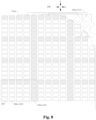
Fig. 7 shows a schematic arrangement structure diagram of sub-pixels in area P inFig. 1 in an example; -
Fig. 8 shows a schematic arrangement structure diagram of pixel circuits in area P inFig. 1 in an example; -
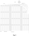
Fig. 9 shows a schematic arrangement structure diagram of pixel circuits in area P inFig. 1 in another example; -
Fig. 10 shows a schematic arrangement structure diagram of sub-pixels in area I inFig. 1 in an example; -
Fig. 11 shows a schematic arrangement structure diagram of pixel circuits in area I inFig. 1 in an example; -
Fig. 12 shows a schematic arrangement structure diagram of sub-pixels in area II inFig. 1 in an example; -
Fig. 13 shows a schematic arrangement structure diagram of pixel circuits in area II inFig. 1 in an example; -
Fig. 14 shows a schematic arrangement structure diagram of pixel circuits in area I inFig. 1 in another example; -
Fig. 15 shows a partial cross-sectional view at C-C inFig. 2 . - In an electronic device such as a mobile phone and a tablet computer, photosensitive components such as a front camera, an infrared light sensor, and a proximity light sensor need to be integrated at a side of the display panel. In some embodiments, a light-transmitting display area may be arranged on the electronic device and the photosensitive components may be arranged at the back of the light-transmitting display area, so that a full-screen display can be achieved for the electronic device while ensuring that the photosensitive components operate normally.
- In order to increase the light transmittance of the light-transmitting display area, the driving circuits for the light-transmitting area are usually arranged in a non-light-transmitting area, which causes non-uniform display in the non-light-transmitting area of the display panel.
- In order to solve the problems described above, the embodiments of the present application provide a display panel and a display apparatus, which will be described below with reference to the accompanying drawings.
- The embodiments of the present application provide a
display panel 100, which may be an organic light emitting diode (OLED)display panel 100. - Reference is made to
Fig. 1 to Fig. 3 together, in whichFig. 1 shows a schematic top view of adisplay panel 100 according to the embodiments of the present application,Fig. 2 shows a partial enlarged schematic structural diagram of area Q inFig. 1 , andFig. 3 shows a partial enlarged schematic structural diagram of area Q inFig. 1 in another example.Fig. 2 andFig. 3 illustrate different layer structures.Fig. 2 illustrates an arrangement structure diagram ofsub-pixels 110a in Q inFig. 1 , andFig. 3 differs fromFig. 2 in thatFig. 3 illustrates an arrangement structure diagram ofpixel circuits 120a in a second display area AA2 in Q, and further illustrates a schematic arrangement structure diagram of thesub-pixels 110a in a first display area AA1. - As shown in
Fig. 1 to Fig. 3 , the embodiments of the first aspect of the present application provide adisplay panel 100 including the first display area AA1 and the second display area AA2, and thedisplay panel 100 includes: a plurality of sub-pixels including a plurality offirst sub-pixels 111 located in the first display area AA1 and a plurality ofsecond sub-pixels 112 located in the second display area AA2; a plurality ofpixel blocks 110 including the plurality of sub-pixels, each of thepixel blocks 110 including asub-pixels 110a of the plurality of sub-pixels, the plurality ofsub-pixels 110a including a plurality offirst sub-pixels 111 located in the first display area AA1 and a plurality ofsecond sub-pixels 112 located in the second display area AA2; and a plurality ofcircuit blocks 120 located in the second display area AA2, each of thecircuit blocks 120 includingb pixel circuits 120a, theb pixel circuits 120a includingfirst circuits 121 andsecond circuits 122, at least part of thefirst circuits 121 being configured to drive thefirst sub-pixels 111, and thesecond circuits 122 being configured to drive thesecond sub-pixels 112; herein both a and b are positive integers greater than 0, and a is less than b, in the second display area AA2, an orthographic projection of thecircuit block 120 in a thickness direction of thedisplay panel 100 is located within an orthographic projection of thepixel block 110 in the thickness direction. The structures of thepixel block 110 and thecircuit block 120 are defined by rectangular boxes inFig. 2 andFig. 3 , but the structure of thedisplay panel 100 in the present application is not limited by the rectangular boxes. The rectangular box includes a small portion of asub-pixel 110a which does not belong to asame pixel block 110, and a sub-pixel 100a with an area within the rectangular box greater than 50% of a total area of the sub-pixel 100a is thesub-pixel 110a within thepixel block 110 represented by the rectangular box. - All of the a
sub-pixels 110a in eachpixel block 110 located in the first display area AA1 are thefirst sub-pixels 111, and all of the asub-pixel 110a in eachpixel block 110 located in the second display area AA2 are thesecond sub-pixel 112. - In the
display panel 100 according to the embodiments of the first aspect of the present application, thecircuit blocks 120 are located in the second display area AA2, that is, thepixel circuits 120a for driving thefirst sub-pixels 111 and thesecond sub-pixels 112 are all located in the second display area AA2, so that the light transmittance of the first display area AA1 can be greater than the light transmittance of the second display area AA2. Photosensitive components may be integrated at the back of the first display area AA1 of thedisplay panel 100 to achieve under-screen integration for the photosensitive components such as cameras. Alternatively, driving circuits such as a shift register of thedisplay panel 100 may be arranged in the first display area AA1 to achieve a narrow frame design for thedisplay panel 100. - In the
display panel 100 according to the embodiments of the first aspect of the present application, thecircuit blocks 120 are located in the second display area AA2, each of thecircuit blocks 120 includesb pixel circuits 120a, thepixel block 110 includes asecond sub-pixels 112 located in the second display area AA2, b is greater than a, asecond circuits 122 are arranged in thecircuit block 120 so as to drive the asecond sub-pixels 112 in thepixel block 110, (b-a)first circuits 120 may be arranged in thecircuit block 120, and at least part of thefirst circuits 121 in thecircuit block 120 can be used to drive thefirst sub-pixels 111 in the first display area AA1. An orthographic projection of thecircuit block 120 in a thickness direction of thedisplay panel 100 is located within an orthographic projection of thepixel block 110 in the thickness direction. On the one hand, it can be guaranteed that in the second display area AA2, the arrangement of a plurality ofsecond circuits 122 in thecircuit block 120 is the same as the arrangement of a plurality ofsecond sub-pixels 112 in thepixel block 110, the arrangement of thecircuit blocks 120 is more uniform, and the display effect of the second display area AA2 is improved. On the other hand, the distance between thesecond circuit 122 in at least part of thecircuit blocks 120 and thesecond sub-pixel 112 driven by thesecond circuit 122 can be reduced, the length of the wirings between at least part of thesecond circuits 122 and thesecond sub-pixels 112 can be reduced, and the signal transmission stability is guaranteed. - Optionally, the
pixel block 110 in the second display area AA2 includes asecond sub-pixels 112, and thepixel block 110 in the first display area AA1 includes afirst sub-pixels 111. If a part of display area is located between the first display area AA1 and the second display area AA2, thepixel block 110 between the first display area AA1 and the second display area AA2 may further include thefirst sub-pixels 111 and thesecond sub-pixel 112, and a sum of the number of thefirst sub-pixels 111 and the number of thesecond sub-pixels 112 is a. - Optionally, the
circuit block 120 may include bfirst circuits 121 or bsecond circuits 122. In some other embodiments, thepixel circuit 120a may include both thefirst circuit 121 and thesecond circuit 122, and a sum of the number of thefirst circuits 121 and the number of thesecond circuits 122 is b. - In some optional embodiments, in the second display area AA2, an area of the orthographic projection of the
pixel block 110 in the thickness direction overlaps the orthographic projection of thecircuit block 120 in the thickness direction, so that the area of thepixel circuits 120a in thepixel block 110 is relatively great. - Optionally, still referring to
Fig. 3 , a distribution area of thefirst circuit 121 is equal to a distribution area of thesecond circuit 122, so that the display effect of the second display area AA2 can be further improved, and display difference due to different distribution areas of thefirst circuit 121 and thesecond circuit 122 can be avoided. Optionally, a circuit structure of thefirst circuit 121 is the same as a circuit structure of thesecond circuit 122, but thefirst circuit 121 is configured to drive thefirst sub-pixel 111, while thesecond circuit 122 is configured to drive thesecond sub-pixel 112. - The orthographic projection of the
circuit block 120 in the thickness direction of thedisplay panel 100 is the orthographic projection of thecircuit block 120 on a display surface of thedisplay panel 100. The orthographic projection of thepixel block 110 in the thickness direction is the orthographic projection of thepixel block 110 on the display surface of thedisplay panel 100. - Optionally, the orthographic projection of the
pixel block 110 in the thickness direction of thedisplay panel 100 is an area where the orthographic projections of the a sub-pixels 110a in thepixel block 110 in the thickness direction of thedisplay panel 100 are located. For example, under a condition that thesub-pixels 110a are arranged to form a pixel arrangement structure, the area where thepixel block 110 is located is the arrangement area occupied by the a sub-pixels 110a in the pixel arrangement structure. For example, under a condition that the size of the pixel arrangement structure is 10cm×10cm and the sub-pixels 110a in the pixel arrangement structure are distributed in 10 rows and 10 columns, the arrangement size of asingle sub-pixel 110a is 1cm×1cm, that is, the size of the orthographic projection of asingle sub-pixel 110a in the thickness direction of thedisplay panel 100 is 1cm×1cm, and the area where thepixel block 110 is located is an area formed by a areas of 1cm×1cm. This is merely for illustration and does not mean that the actual arrangement size of the sub-pixel 110a is 1cm×1cm. - The a sub-pixels 110a in the
pixel block 110 are arranged adjacently. For example, as shown inFig. 2 andFig. 3 , if a is equal to 16 and thepixel block 110 includes 16 sub-pixels 110a, the 16 sub-pixels 110a inpixel block 110 are arranged adjacently. The 16sub-pixels 110a may be located in a same row or two or more adjacent rows. - Optionally, as shown in
Fig. 2 andFig. 3 , under a condition that twosub-pixels 110a adjacent in a row direction and/or a column direction overlap, the area where the orthographic projection of the a sub-pixels 110a in the thickness direction of thedisplay panel 100 is located is of an average arrangement size of the a sub-pixels 110a. The row direction may be a first direction X, and the column direction may be a second direction Y In some other embodiments, the row direction may be the second direction Y, and the column direction may be the first direction X. - Optionally, as shown in
Fig. 2 , the sub-pixels 110a of thedisplay panel 100 are arranged to form a pixel arrangement structure which includes a plurality of repeating units, the repeating unit includes a plurality of sub-pixels 110a, and the repeating units are arranged repeatedly in the row direction and the column direction to form the pixel arrangement structure. The number of the sub-pixels 110a included in thepixel block 110 may be related to the number of the sub-pixels 110a included in the repeating unit, for example, the number of the sub-pixels 110a included in thepixel block 110 is an integral multiple of the number of the sub-pixels 110a included in the repeating unit. For example, as shown inFig. 2 , under a condition that the repeating unit includes four sub-pixels 110a, thepixel block 110 includes sixteen sub-pixels 110a, the number of the sub-pixels 110a included in thepixel block 110 is four times as many as the number of the sub-pixels 110a included in the repeating unit, that is, thepixel block 110 includes four repeating units, and the orthographic projection of thepixel block 110 in the thickness direction is the arrangement size occupied by the four repeating units. - Optionally, the orthographic projection of the
circuit block 120 in the thickness direction of thedisplay panel 100 is an area where the orthographic projection of the b sub-pixels 110a in thecircuit block 120 in the thickness direction is located. Theb pixel circuits 120a in thecircuit block 120 are arranged adjacently. For example, under a condition that b is equal to 25 and thecircuit block 120 includes 25pixel circuits 120a, the 25pixel circuits 120a are arranged adjacently. The 25pixel circuits 120a may be located in a same row or two or more rows. - Optionally, under a condition that the a sub-pixels 110a in the
pixel block 110 are arranged in a same row, theb pixel circuits 120a in thecircuit block 120 are arranged in a same row. Thepixel circuits 120a incircuit block 120 are compressed in the row direction, so that the orthographic projection of theb pixel circuits 120a in the thickness direction is located within the orthographic projection of the a sub-pixels 110a in the thickness direction. - In some optional embodiments, the
pixel block 110 includes a plurality of the sub-pixels 110a distributed in p rows and q columns, and a product of p and q is a; thecircuit block 120 includes a plurality of thepixel circuits 120a distributed in e rows and f columns, and a product of e and f is b, in which p, q, e and f are all positive integers greater than 1, e ≥ p andf ≥ q. - In these optional embodiments, p, q, e and f are all positive integers greater than 1, and thus the
pixel block 110 includes the sub-pixels 110a arranged in a plurality of rows and a plurality of columns, and thecircuit block 120 includes thepixel circuits 120a arranged in a plurality of rows and a plurality of columns, so that thepixel circuits 120a are compressed in both the row direction and the column direction, thereby avoiding the technical difficulty due to the compression of thepixel circuits 120a in a same direction. - P, q, e and f may be set in a variety of ways, and in some optional embodiments, p is equal to q, e is equal to f, and e is greater than p. That is, the
pixel block 110 includes p rows and p columns of the sub-pixels 1 10a, and thecircuit block 120 includes e rows and e columns of thepixel circuits 120a, so that the plurality of sub-pixels 110a in thepixel block 110 are arranged more regularly and the plurality ofpixel circuits 120a in thecircuit block 120 are arranged more regularly, and the size of thepixel circuits 120a can be adjusted more easily. - As described above, as shown in
Fig. 2 andFig. 3 , for example, under a condition that a is equal to 16 and thepixel block 110 includes 16 sub-pixels 110a, thepixel block 110 includes 4 rows and 4 columns of the sub-pixels 110a. Under a condition that b is equal to 25 and thecircuit block 120 includes 25pixel circuits 120a, thecircuit block 120 includes 5 rows and 5 columns of thepixel circuits 120a. - In the
display panel 100 according to the embodiments of the present application, in the second display area AA2, five rows and five columns of thepixel circuits 120 are arranged in an area where four rows and four columns of thesub-pixels 110a are located. The number of thepixel circuits 120a arranged in the area where the four rows and four columns of thesub-pixels 110a are located is greater than the number of the sub-pixels 110a, and at least part of one row and one column of thepixel circuits 120a that are spare in the area where the four rows and four columns of thesub-pixels 110a are located may be configured to drive the first sub-pixels 111 in the first display area AA1. - Reference is made to
Fig. 1 to Fig. 5 together, in whichFig. 4 shows a schematic arrangement structure diagram of the sub-pixels 110a in W inFig. 1 , andFig. 5 shows a schematic arrangement structure diagram of thepixel circuits 120a in W inFig. 1 . - In some optional embodiments, as shown in
Fig. 1 to Fig. 5 , the second display area AA2 includes a main display area ZA and a transition display area TA located between the main display area ZA and the first display area AA1, and at least part of thefirst circuits 121 located in the transition display area TA are configured to drive thefirst sub-pixels 111. That is, thefirst circuits 121 for driving the first sub-pixels 111 are located in the transition display area TA, and thefirst circuits 121 which are not configured to drive the first sub-pixels 111 are located in the main display area ZA. - In these optional embodiments, the
first circuits 121 for driving the first sub-pixels 111 are arranged in the transition display area TA which is closer to the first display area AA1, so that the distance between thefirst circuit 121 and thefirst sub-pixel 111 which are electrically connected with each other can be reduced, the length of the connecting line between thefirst circuit 121 and thefirst sub-pixel 111 can be reduced, and the signal transmission stability is guaranteed. - Optionally, the
circuit block 120 in the main display area ZA is located within the orthographic projection of thepixel block 110 driven by thecircuit block 120, and thecircuit block 120 in the main display area ZA includes p rows and q columns of thesecond circuits 122 and (e-p) rows and (f-q) columns of thefirst circuits 121. Herein, (e-p) rows and (f-q) columns of thefirst circuits 121 refers to the (e-p) rows and (f-q) columns from the e rows and f columns of thecircuit block 120. - For example, still referring to
Fig. 4 andFig. 5 , under a condition that thepixel block 110 includes four rows and four columns of the sub-pixels 110a, each row includes four sub-pixels 110a and each column includes four sub-pixels 110a, and thecircuit block 120 includes five rows and five columns of thepixel circuits 120a, eachcircuit block 120 in the main display area ZA includes four rows and four columns of thesecond circuits 122 and one row and one column of thefirst circuits 121, which refer to one row and one column of thefirst circuits 121 from the five rows and five columns of thepixel circuits 120a. In the one row and one column of thefirst circuits 121, the one row of thefirst circuits 121 include fivefirst circuits 121, the one column of thefirst circuits 121 also include fivefirst circuits 121, and onefirst circuit 121 is repeated at the intersection position of the one row and one column of thefirst circuits 121. Therefore, eachcircuit block 120 in the main display area ZA includes 16second circuits 122 and 9first circuits 121. - In these optional embodiments, the number of the
second circuits 122 included in thecircuit block 120 in the main display area ZA is the same as the number of the second sub-pixels 112 included in thepixel block 110, so that thesecond circuits 122 in each circuit block 120 can be configured to drive the second sub-pixels 112 in eachpixel block 110. Thecircuit block 120 in the main display area ZA is located within the orthographic projection of thepixel block 110 driven by thecircuit block 120, so that the distance between thesecond circuit 122 and thesecond sub-pixel 112 driven by thesecond circuit 122 can be reduced, and the length of the connecting line between thesecond circuit 122 and thesecond sub-pixel 112 driven by thesecond circuit 122 can be reduced. - Optionally, in the main display area ZA, a relative position relationship of the plurality of
second circuits 122 in thecircuit block 120 is the same as a relative position relationship of the plurality of second sub-pixels 112 in thepixel block 110, so that the distance between thesecond circuit 122 and thesecond sub-pixel 112 driven by thesecond circuit 122 can be further reduced, and the length of the connecting line between thesecond circuit 122 and thesecond sub-pixel 112 driven by thesecond circuit 122 can be reduced. - Optionally, the relative position relationship of the
second circuits 122 in the main display area ZA and the second sub-pixels 112 driven by thesecond circuits 122 may be arranged in a variety of ways. - For example, the orthographic projection of the
second circuit 122 in the thickness direction at least partially overlaps the orthographic projection of thesecond sub-pixel 112 driven by thesecond circuit 122 in the thickness direction, so that the distance between thesecond circuit 122 and thesecond sub-pixel 112 driven by thesecond circuit 122 can be further reduced, and the length of the connecting line between thesecond circuit 122 and thesecond sub-pixel 112 driven by thesecond circuit 122 can be reduced. - Alternatively, the orthographic projection of the
second circuit 122 in the thickness direction is staggered with the orthographic projection of thesecond sub-pixel 112 driven by thesecond circuit 122 in the thickness direction, as long as the orthographic projection in the thickness direction of thecircuit block 120 where thesecond circuit 122 is located is located within the orthographic projection in the thickness direction of thepixel block 110 where thesecond sub-pixel 112 driven by thesecond circuit 122 is located. - Optionally, as shown in
Fig. 5 , thefirst circuit 121 in thecircuit block 120 is located at a side of thesecond circuit 122 in the row direction, or thefirst circuit 121 is located at a side of the plurality ofsecond circuits 122 in the column direction. - In some other embodiments, in the main display area ZA, the
first circuit 121 is located in the middle of the plurality ofsecond circuits 122 in the row direction and/or column direction, so that the staggered size between thesecond circuit 122 and thesecond sub-pixel 112 driven by thesecond circuit 122 is reduce, and the wiring length between thesecond circuit 122 and thesecond sub-pixel 112 driven by thesecond circuit 122 is reduced. - In the transition display area TA, the
first circuits 121 and thesecond circuits 122 may be arranged in a variety of ways. In some optional embodiments, still referring toFig. 3 to Fig. 5 , the arrangement of thefirst circuits 121 and thesecond circuits 122 in the transition display area TA is the same as the arrangement of thefirst circuits 121 and thesecond circuits 122 in the main display area ZA. That is, thecircuit block 120 in the transition display area TA is located within the orthographic projection of thepixel block 110 driven by thecircuit block 120, and thecircuit block 120 in the transition display area TA includes p rows and q columns of thesecond circuits 122 and (e-p) rows and (f-q) columns of thefirst circuits 121. Therefore, the display difference between the transition display area TA and the main display area ZA can be further reduced, the distance between thesecond circuit 122 in the transition display area TA and thesecond sub-pixel 112 driven by thesecond circuit 122 can be reduced, and the length of the connecting line between thesecond circuit 122 and thesecond sub-pixel 112 driven by thesecond circuit 122 can be reduced. - Optionally, in the transition display area TA, a further relative position relationship of the plurality of
second circuits 122 in thecircuit block 120 is the same as a further relative position relationship of the plurality of second sub-pixels 112 in thepixel block 110, so that the distance between thesecond circuit 122 in the transition display area TA and thesecond sub-pixel 112 driven by thesecond circuit 122 is reduced, and the length of the connecting line between thesecond circuit 122 and thesecond sub-pixel 112 driven by thesecond circuit 122 is reduced. - In the transition display area TA, the
first circuits 121 may be arranged in a variety of ways. In some optional embodiments, thefirst circuits 121 include a plurality ofrow circuits 121a arranged side by side in a row direction andcolumn circuits 121b arranged side by side in a column direction, and at least part of therow circuits 121a and/or thecolumn circuits 121b are configured to drive thefirst sub-pixels 111. Therow circuits 121a refer to a plurality of thefirst circuits 121 arranged in the row direction, and thecolumn circuits 121b refer to a plurality of thefirst circuits 121 arranged in the column direction. The row direction and the column direction intersect, so thefirst circuit 121 at the intersection position may be either therow circuit 121a or thecolumn circuit 121b. - In these optional embodiments, no
second circuit 122 is arranged in the row where therow circuits 121a are located, and nosecond circuit 122 is arranged in the column where thecolumn circuits 121b are located. When the first sub-pixels 111 are driven by therow circuits 121a and/or thecolumn circuits 121b, the crosstalk between the connecting line between thefirst sub-pixel 111 and thesecond circuit 122 and the connecting line between thesecond sub-pixel 112 and thesecond circuit 122 can be avoided. - For example, the distribution pattern of the
first circuits 121 is grid shaped and includes a hollow area in which a plurality ofsecond circuits 122 are located, that is, at least two of thefirst circuits 121 are arranged at intervals, at least part of thesecond circuits 122 are located between two adjacentfirst circuits 121, and thefirst circuits 121 are arranged around the plurality of thesecond circuits 122. That is, in thecircuit block 120, thefirst circuits 121 are concentrated in a same row and a same column, so that the arrangement of the plurality ofsecond circuits 122 in thecircuit block 120 is more concentrated. - The first display area AA1 may be arranged in a variety of ways. For example, still referring to
Fig. 1 , the first display area AA1 includes a regularly shaped area and an irregularly shaped area located at at least one side of the regularly shaped area in the row direction, and at least part of the first sub-pixels 111 in the irregularly shaped area and at least part of the first sub-pixels 111 in the regularly shaped area are arranged in a same row. - The irregularly shaped area may be arranged in a variety of ways. Still referring to
Fig. 1 , for example, the irregularly shaped area may include a corner area RA arranged around the second display area AA2 and being bent. Under a condition that the first display area AA1 includes the corner area RA, thepixel circuit 120a corresponding to thefirst sub-pixel 111 in the corner area RA is located in the second display area AA2, so that driving circuits such as a shift register and driving signal lines may be further arranged in the corner area RA, the frame size of thedisplay panel 100 can be reduced. - Optionally, still referring to
Fig. 1 , the irregularly shaped area may further include a photosensitive area UDC, and the second display area AA2 is arranged around at least part of the photosensitive area UDC. Under a condition that the first display area AA1 includes the photosensitive area UDC, thepixel circuit 120a corresponding to thefirst sub-pixel 111 in the photosensitive area UDC is located in the second display area AA2, so that the light transmittance of the photosensitive area UDC can be increased, which facilitates the under-screen integration of the photosensitive components in the photosensitive area UDC. Moreover, the photosensitive area UDC can display images, the display area of the display panel is increased, and a full-screen design is achieved for the display apparatus. - Optionally, still referring to
Fig. 1 , the first display area AA1 includes a frame display area BA arranged around the second display area AA2 and including an end frame display area BA1 located at at least one side of the second display area AA2 in a column direction and a side frame display area BA2 located at at least one side of the second display area AA2 in a row direction. Under a condition that the first display area AA1 includes the frame display area BA, thepixel circuit 120a corresponding to thefirst sub-pixel 111 in the frame display area BA is located in the second display area AA2, so that driving circuits such as a shift register and driving signal lines may be further arranged in the frame display area BA, the frame size of thedisplay panel 100 can be reduced, and a narrow frame design or even a frame-free design can be achieved for thedisplay panel 100. - Optionally, the regularly shaped area may include the above frame display area BA, and the regularly shaped area may further include a part of the first display area AA1 located at at least one side of the photosensitive area UDC in the row direction. Under a condition that the irregularly shaped area includes the corner area RA, the corner area RA may be connected between the end frame display area BA1 and the side frame display area BA2 that are adjacent.
- The first sub-pixels 111 located in different areas may be driven by different
first circuits 121. In some optional embodiments, still referring toFig. 3 , at least part of therow circuits 121a are configured to drive the first sub-pixels 111 located in the irregularly shaped area. Therefore, the first sub-pixels 111 in a same row in the irregularly shaped area may be driven by therow circuits 121a in a same row, which can simplify the wiring between thefirst sub-pixels 111 and therow circuits 121a. In addition, the first sub-pixels 111 in the irregularly shaped area are driven by therow circuits 121a, only a row signal line for transmitting driving signals to therow circuits 121a needs be to added, and no additional column signal line is necessary, so that the number of signal lines in the second display area AA2 can be reduced. - As shown in
Fig. 2 andFig. 3 , under a condition that the first display area AA1 includes the photosensitive area UDC, the first sub-pixels 111 in the photosensitive area UDC may be driven by therow circuits 121a. Optionally, as shown inFig. 3 , various rows of the first sub-pixels 111 in the first display area AA1 may be driven by therow circuits 121a in different rows, that is, the first sub-pixels 111 in different rows are driven by therow circuits 121a in different rows. In some other embodiments, referring toFig. 6 , a plurality of rows of the first sub-pixels 111 in the first display area AA1 may be driven by therow circuits 121a in a same row, that is, two or more rows of the first sub-pixels 111 may be driven by therow circuits 121a in a same row. - Optionally, under a condition that the first sub-pixels 111 in the irregularly shaped area are driven by the
row circuits 121a in the transition display area TA, a row signal line may be added in the transition display area TA to transmit driving signals to therow circuits 121a. - In some optional embodiments, still referring to
Fig. 6 , thedisplay panel 100 further includes firstrow signal lines 131 and secondrow signal lines 132, the firstrow signal lines 131 are connected with therow circuits 121a for driving thefirst sub-pixels 111 and configured to transmit signals to therow circuits 121a, and the secondrow signal lines 132 are connected with thesecond circuits 122 and configured to transmit signals to thesecond circuits 122. In these optional embodiments, the firstrow signal lines 131 are added to transmit driving signals to therow circuits 121a, thereby enabling therow circuits 121a to drive the first sub-pixels 111 to display. - Reference is made to
Fig. 1 ,Fig. 7 andFig. 8 , in whichFig. 7 shows a schematic arrangement structure diagram of the sub-pixels 110a in P inFig. 1 , andFig. 8 shows a schematic structural diagram of thepixel circuits 120a in P inFig. 1 . Herein, the first sub-pixels 111 in the corner area RA are illustrated inFig. 8 . - As shown in
Fig. 7 andFig. 8 , under a condition that the first display area AA1 includes the corner area RA, the first sub-pixels 111 in the corner area RA may be driven by therow circuits 121a in the second display area AA2. As shown inFig. 8 , a plurality of rows of the first sub-pixels 111 in the corner area RA may be driven by a plurality of rows of therow circuits 121a. Alternatively, as shown inFig. 9 , a plurality of rows of the first sub-pixels 111 in the corner area RA may be driven by therow circuits 121a in a same row. - Optionally, the
display panel 100 further includes column signal lines (not shown) extending in the column direction and configured to transmit driving signals to thefirst circuits 121 and/or thesecond circuits 122 arranged in a same column. - Optionally, the first
row signal lines 131 and the secondrow signal lines 132 may be scanning signal lines, and the column signal lines may be data signal lines. In some other optional embodiments, the firstrow signal lines 131 and the secondrow signal lines 132 may be data signal lines, and the column signal lines may be scanning signal lines. - In some optional embodiments, the
display panel 100 further includes a row buffer (not shown) for storing driving signals for the first sub-pixels 111 in the irregularly shaped area and transmitting driving signals to the firstrow signal lines 131 according to the driving signals for the first sub-pixels 111 in the irregularly shaped area. By adding the row buffer which stores driving signals for the first sub-pixels 111 in the irregularly shaped area, the row buffer can transmit driving signals to the firstrow signal lines 131, thereby driving therow circuits 121a through the first row signal lines 131. - Optionally, the
display panel 100 includes a pixel jump reduction (PJR) processing module, which can copy and move images. On the basis that the image data has been processed according to the arrangement of thefirst sub-pixel 111 and thesecond sub-pixel 112, data corresponding to thefirst sub-pixel 111 is added in the image data at the position where therow circuit 121a for driving thefirst sub-pixel 111 is located, and these data are stored in the row buffer. - Optionally, the PJR processing module is connected with a digital to analog conversion module, so as to convert the image data to an analog voltage signal through the digital to analog conversion module.
- Optionally, under a condition that a plurality of the first sub-pixels 111 form a display unit emitting white light and two adjacent display units share one
first sub-pixel 111, thisfirst sub-pixel 111 may be driven to emit light through thefirst circuits 121 located in the second display area AA2 according to the light emitting requirements of the display unit. - Reference is made to
Fig. 1 andFig. 10 toFig. 13 ,Fig. 10 shows a schematic arrangement structure diagram of the sub-pixels 110a in I inFig. 1 ,Fig. 11 shows a schematic arrangement structure diagram of thepixel circuits 120a in I inFig. 1 , in which the first sub-pixels 111 located in the end frame display area BA1 are also illustrated,Fig. 12 shows a schematic arrangement structure diagram of the sub-pixels 110a in II inFig. 1 , andFig. 13 shows a schematic arrangement structure diagram of thepixel circuits 120a in II inFig. 1 , in which the first sub-pixels 111 located in the side frame display area BA2 are also illustrated. - The first sub-pixels 111 in the frame display area BA are arranged in rows and columns. For example, as shown in
Fig. 10 , the first sub-pixels 111 in the end frame display area BA1 are arranged in a plurality of rows, and the number of the first sub-pixels 111 arranged in a same row in the end frame display area BA1 is less than or equal to the number of therow circuits 121a arranged in a same row in the transition display area TA. Therefore, the first sub-pixels 111 in a same row in the end frame display area BA1 can be driven by therow circuits 121a arranged in a same row in the transition display area TA, and the row signal lines originally for driving the first sub-pixels 111 in a same row in the end frame display area BA1 can be moved to the transition display area TA and connected with therow circuits 121a for driving thefirst sub-pixels 111. - For example, as shown in
Fig. 12 , the first sub-pixels 111 in the side frame display area BA2 are arranged in a plurality of columns, and the number of the first sub-pixels 111 arranged in a same column in the side frame display area BA2 is less than or equal to the number of thecolumn circuits 121b arranged in a same column in the transition display area TA. Therefore, the first sub-pixels 111 in a same column in the side frame display area BA2 can be driven by therow circuits 121a arranged in a same column in the transition display area TA, and the column signal lines originally for driving the first sub-pixels 111 in a same column in the side frame display area BA2 can be moved to the transition display area TA and connected with thecolumn circuits 121b for driving thefirst sub-pixels 111. - In some optional embodiments, as shown in
Fig. 10 to Fig. 13 , at least part of therow circuits 121a are configured to drive the first sub-pixels 111 located in the end frame display area BA1, and/or at least part of thecolumn circuits 121b are configured to drive the first sub-pixels 111 located in the side frame display area BA2. No additional row signal line or column signal line is necessary, and the wiring of the signal lines of thedisplay panel 100 can be further simplified. - The above describes how to use the
first circuits 121 in the transition display area TA to drive thefirst sub-pixels 111 under a condition that the arrangement of the circuit blocks 120 in the transition display area TA is the same as the arrangement of the circuit blocks 120 in the main display area ZA. - In some other optional embodiments, the arrangement of the circuit blocks 120 in the transition display area TA may be different from the arrangement of the circuit blocks 120 in the main display area ZA.
- Reference is made to
Fig. 14 , which shows a schematic arrangement structure diagram of pixel circuits in area I inFig. 1 in another example. - Optionally, as shown in
Fig. 14 , thefirst circuits 121 in the transition display area TA are all located at a side of thesecond circuits 122 close to thefirst sub-pixels 111. In these optional embodiments, thefirst circuits 121 in the transition display area TA are arranged closer to the first display area AA1, which can reduce the distance between thefirst circuit 121 and thefirst sub-pixel 111 driven by thefirst circuit 121. - Optionally, a position relationship of the
second circuit 122 for driving thesecond sub-pixel 112 in the transition display area TA and thefirst circuits 121 in the transition display area TA for driving thefirst sub-pixels 111 is the same as a position relationship of the second sub-pixels 112 in the transition display area TA and the first sub-pixels 111 in the first display area AA1. In this way, the distance between thesecond circuit 122 in the transition display area TA and thesecond sub-pixel 112 driven by thesecond circuit 122 and the distance between thefirst circuit 121 and thefirst sub-pixel 111 driven by thefirst circuit 121 can be reduced, and the intersection between the signal line for connecting thefirst circuit 121 and thefirst sub-pixel 111 and the signal line for connecting thesecond circuit 122 and thesecond sub-pixel 112 can be avoided, which simplifies the wiring of the signal lines. - Furthermore, in these optional embodiments, no additional row signal line or column signal line is necessary, it is only needed that the signal line for driving the
first sub-pixel 111 is connected with thefirst circuit 121 for driving thefirst sub-pixel 111. The plurality offirst circuits 121 in the transition display area TA are arranged according to the arrangement of the plurality of first sub-pixels 111 driven by the plurality offirst circuits 121, and the plurality offirst circuits 121 are connected with the first sub-pixels 111 in sequence, so that the lengths of a plurality of signal lines for connecting thefirst circuits 121 and the first sub-pixels 111 tend to be the same, and the plurality of signal lines can be prevented from intersecting with each other. - Only the connection relationship between the
first sub-pixels 111 and thefirst circuits 121 in the end frame display area BA1 is illustrated inFig. 14 . - In some other embodiments, the first display area AA1 may further include a corner area RA, a photosensitive area UDC and a side frame display area BA2, and the
first circuits 121 for driving the first sub-pixels 111 in the corner area RA, the photosensitive area UDC and the side frame display area BA2 are located at a side of thesecond circuits 122 close to the corner area RA, the photosensitive area UDC and the side frame display area BA2. That is, the first sub-pixels 111 in the corner area RA, the photosensitive area UDC and the side frame display area BA2 may also be connected with thefirst circuits 121 in the transition display area TA in sequence, and a relative position relationship of the first sub-pixels 111 in the corner area RA, the photosensitive area UDC and the side frame display area BA2 and the second sub-pixels 112 in the transition display area TA is the same as a relative position relationship of thefirst circuits 121 for driving the first sub-pixels 111 in the corner area RA, the photosensitive area UDC and the side frame display area BA2 and thesecond circuits 122 in the transition display area TA. - Reference is made to
Fig. 15 , which shows a cross-sectional view at C-C inFig. 3 . - In some optional embodiments, as shown in
Fig. 15 , thedisplay panel 100 further includes: asignal line layer 103 including firstconnection signal lines 133 for connecting thefirst circuits 121 and thefirst sub-pixels 111. - In these optional embodiments, the crosstalk between the first
connection signal line 133 and other signal lines can be avoided by arranging thesignal line layer 103. - Optionally, still referring to
Fig. 15 , thedisplay panel 100 further includes asubstrate 101, an array base plate arranged on thesubstrate 101, and apixel definition layer 102, in which thepixel circuits 120a are arranged in the array base plate. Thepixel definition layer 102 includes a first pixel opening K1 located in the first display area AA1 and a second pixel opening K2 located in the second display area AA2. Thefirst sub-pixel 111 includes a first light-emittingstructure 111b located in the first pixel opening K1, afirst electrode 111a located at a side of the first light-emittingstructure 111b facing the array base plate, and asecond electrode 111c located at a side of the first light-emittingstructure 111b away from the array base plate. Thesecond sub-pixel 112 includes a second light-emittingstructure 121b located in the second pixel opening K2, athird electrode 121a located at a side of the second light-emittingstructure 121b facing the array base plate, and afourth electrode 121c located at a side of the second light-emittingstructure 121b away from the array base plate. Thefirst electrode 111a and thethird electrode 121a are, for example, pixel electrodes, and thesecond electrode 111c and thefourth electrode 121c may be interconnected as a common electrode. - Optionally, the
signal line layer 103 may be located between the array base plate and a light-emitting layer. The array base plate may include a first metal layer, a second metal layer and a third metal layer, and thepixel circuit 120a includes a thin film transistor (TFT), which may be a switching thin film transistor and a driving thin film transistor. The thin film transistor (TFT) includes a semiconductor layer, a gate, a source electrode, and a drain electrode, in which the gate may be located in the first metal layer, and the source electrode and the drain electrode may be located in the third metal layer. One electrode plate of a capacitor may be arranged in the second metal layer, and the other electrode plate of the capacitor may be located in the first metal layer or the third metal layer. - Optionally, the row signal line is a scanning line and may be located in the first metal layer and interconnected with the gate of the switching thin film transistor. Optionally, the
display panel 100 further includes a column signal line which is a data line and located in the third metal layer, and the column signal line may be interconnected with one of the source electrode and the drain electrode of the switching thin film transistor. - Optionally, the source electrode and the drain electrode of the driving thin film transistor of part of the
first circuits 121 are connected with thefirst electrode 111a of thefirst sub-pixel 111 through the firstconnection signal line 133. - In some optional embodiments, still referring to
Fig. 14 , at least part of the firstconnection signal line 133 extends in the second direction Y, and the part of the firstconnection signal line 133 extending in the second direction Y is located in a same film layer. An arrangement size of the firstconnection signal line 133 in the first direction X is m µm, an arrangement size in the first direction X of thefirst sub-pixel 111 adjacent to the second display area AA2 along the second direction Y is n µm, 2k first sub-pixels 111 are arranged in the second direction Y in the first display area AA1, and m and n satisfy n = km + d, in which k is a positive integer, d is a positive number less than m, and d is redundancy of the signal line spacing. One of the first direction X and the second direction Y is the row direction, and the other one is the column direction. Referring toFig. 14 , in the embodiments of the present application, for example, the first direction X is the row direction, and the second direction Y is the column direction. - The arrangement size of the first
connection signal line 133 in the first direction X includes both an extension size of the firstconnection signal line 133 in the first direction X and a spacing size between two firstconnection signal lines 133 adjacent in the first direction X. The arrangement size of thefirst sub-pixel 111 in the first direction X is an average arrangement size of thefirst sub-pixel 111 in the first direction X. For example, i first sub-pixels 111 are arranged in the first direction X, and the size occupied by the i first sub-pixels 111 in the first direction X is j, then the arrangement size n of thefirst sub-pixels 111 is equal toj/i. - In these optional embodiments, as shown in
Fig. 14 , for example, thefirst sub-pixel 111 adjacent to the second display area AA2 in the second direction Y is an adjoining first sub-pixel 111'. The firstconnection signal lines 133 connected with the first sub-pixels 111 located at a side of the adjoining first sub-pixel 111' away from the second display area AA2 all pass through the adjoining first sub-pixel 111', but the extension size of the adjoining first sub-pixel 11 1' in the first direction X is limited. Therefore, the number of the first sub-pixels 111 arranged in the second direction Y in the first display area AA1 is related to the size of the adjoining first sub-pixel 111', that is, n = km + d. Under a condition that the number of the first sub-pixels 111 arranged in the second direction Y in the first display area AA1 satisfies the above equation, it can be avoided that the firstconnection signal lines 133 adjacent in the first direction X are too close or overlap to cause signal crosstalk. - Optionally, under a condition that the first display area AA1 includes the end frame display area BA1, two end frame display areas BA1 are respectively arranged at two sides of the second display area AA2, then k first sub-pixels 111 are arranged in the second direction Y in one end frame display area BA1. The extension size of the end frame display area BA1 in the second direction Y is less than or equal to the arrangement size of the k first sub-pixels 111 in the second direction Y
- Under a condition that the first display area AA1 is the side frame display area BA2, the first direction X is the column direction, the second direction Y is the row direction, and two side frame display areas BA2 are respectively arranged at two sides of the second display area AA2. Then k first sub-pixels 111 are arranged in the first direction X in one side frame display area BA2, and the extension size of the side frame display area BA2 in the first direction X is less than or equal to the arrangement size of the k first sub-pixels 111 in the first direction X.
- Optionally, under a condition that the first display area AA1 is the photosensitive area UDC and the photosensitive area UDC is circular, the radius of the photosensitive area UDC is less than or equal to the arrangement size of the k first sub-pixels 111 in the row direction.
- For example, the arrangement size of the first
connection signal line 133 in the column direction is 5 µm, the arrangement size of the adjoining first sub-pixel 111' in the column direction is 61.7 µm, then the number of the firstconnection signal lines 133 that can be arranged on the adjoining first sub-pixel 111' is 11 at most, and the extension size of the first display area AA1 in the row direction is less than or equal to the arrangement size of the 11first sub-pixels 111 in the row direction. - In some optional embodiments, still referring to
Fig. 14 , the firstconnection signal line 133 includes afirst segment 133a and asecond segment 133b extending along different directions and located in different film layers, so as to reduce the risk of short circuit between different first connection signal lines 133. - In some optional embodiments, the
signal line layer 103 further includes secondconnection signal lines 134 for connecting thesecond circuits 122 and thesecond sub-pixels 112. The firstconnection signal line 133 and the secondconnection signal line 134 are arranged in a same layer, which can reduce the thickness of thedisplay panel 100. - In some optional embodiments, the plurality of
first circuits 121 for driving the first sub-pixels 111 in a same row are located in a same row, so that the plurality offirst circuits 121 for driving the first sub-pixels 111 in a same row may be connected with a same firstrow signal line 131. - Optionally, the
first circuits 121 in a same row are configured to drive two or more rows of thefirst sub-pixels 111. For example, under a condition that the first display area AA1 includes the irregularly shaped area, therow circuits 121a in the transition display area TA closer to the irregularly shaped area may be configured to drive two or more rows of the first sub-pixels 111 in the irregularly shaped area, so as to reduce the distance between thefirst circuit 121 and thefirst sub-pixel 111 driven by thefirst circuit 121. - In the present application, without changing the original arrangement of the sub-pixels 110a, the first display area AA1 is reserved by arranging the
pixel circuits 120a in the second display area AA2, and the light transmittance of the first display area AA1 can be increased, or other driving circuits and driving signal lines can be arranged in the first display area AA1 so as to reduce the frame size of thedisplay panel 100. In the present application, the arrangement of the circuit blocks 120 is the same as the arrangement of the pixel blocks 110 in the second display area AA2, and display effect at different positions in the second display area AA2 is guaranteed to be uniform. - The embodiments of the present application further provide two arrangements of the
pixel circuits 120a and the manner in which thepixel circuits 120a drive the first sub-pixels 111 to display. - In a first implementation, the arrangement of the circuit blocks 120 in the transition display area TA is the same as the arrangement of the circuit blocks 120 in the main display area ZA, the
row circuits 121a in the transition display area TA are configured to drive the first sub-pixels 111 in the irregularly shaped area, and the firstrow signal lines 131 and the row buffer are added to transmit driving signals to therow circuits 121a in the transition display area TA. On the one hand, this embodiment can ensure that, in the transition display area TA and the main display area ZA, thesecond circuit 122 is close to thesecond sub-pixel 112 driven by thesecond circuit 122, and on the other hand, the row signal line alone is sufficient to drive thefirst sub-pixels 111, so that the wiring of thedisplay panel 100 can be simplified. - In a second implementation, the
pixel block 110 and thecircuit block 120 in the main display area ZA are arranged correspondingly in the thickness direction, the distance between thesecond circuit 122 and thesecond sub-pixel 112 driven by thesecond circuit 122 in the main display area ZA can be reduced. The arrangement of thefirst circuits 121 and thesecond circuits 122 in the transition display area TA is the same as the arrangement of the second sub-pixels 112 in the transition display area TA and the first sub-pixels 111 in the first display area AA1, thecircuit block 120 where thesecond circuit 122 in the transition display area TA is located is staggered with thepixel block 110 where thesecond sub-pixel 112 driven by thesecond circuit 122 is located, and the plurality offirst circuits 121 are connected with the first sub-pixels 111 in sequence, which can not only make the lengths of a plurality of signal lines for connecting thefirst circuits 121 and the first sub-pixels 111 tend to be the same, but also can prevent the plurality of signal lines from intersecting with each other. - Therefore, in the embodiments of the present application, by reducing the size of the
first circuit 121 and the size of thesecond circuit 122, the number of thepixel circuits 120a is greater than the number of the sub-pixels 110a arranged in a same area, and thepixel circuits 120a for driving the first sub-pixels 111 can be arranged in the second display area AA2. Moreover, the width of the first display area AA1 is related to the number of the firstconnection signal lines 133 that can be accommodated in the arrangement size of the adjoining first sub-pixel 111', that is, the number 2k of the first sub-pixels 111 arranged in a same row in the first display area AA1, the arrangement size n of the adjoining first sub-pixel 111' in the row direction, and the arrangement size m of the firstconnection signal line 133 in the row direction satisfy n = km + d. - In some embodiments, the circuit structure of the
first circuit 121 is any of a 2T1C circuit, a 7T1C circuit, a 7T2C circuit, or a 9T1C circuit. Herein, the "2T1C circuit" refers to the pixel driving circuit including two thin film transistors (T) and one capacitor (C), and the same applies to the "7T1C circuit", "7T2C circuit", "9T1C circuit", and so on. - Optionally, the circuit structure of the
second circuit 122 is any one of the 2T1C circuit, the 7T1C circuit, the 7T2C circuit, or the 9T1C circuit. - Optionally, the size of the
first sub-pixel 111 is less than the size of thesecond sub-pixel 112 of a same color, which can reduce the space occupied by the first sub-pixels 111 in the first display area AA1, so that the non-light-emitting area in the first display area AA1 is larger, which is beneficial for increasing the light transmittance of the first display area AA1. - In some optional embodiments, the
first sub-pixels 111 and thefirst circuits 121 are arranged in one-to-one correspondence. Eachfirst sub-pixel 111 is driven by a correspondingfirst circuit 121, which can improve the display effect of thedisplay panel 100. - Optionally, two or more adjacent
first sub-pixels 111 of a same color are connected with a samefirst circuit 121 to facilitate the wiring of thedisplay panel 100. - Optionally, as described above, the
first sub-pixel 111 includes the first light-emittingstructure 111b, thefirst electrode 111a, and thesecond electrode 111c. Thesecond sub-pixel 112 includes the second light-emittingstructure 121b, thethird electrode 121a, and thefourth electrode 121c. In the embodiment, for example, thefirst electrode 111a and thethird electrode 121a are anodes, and thesecond electrode 111c and thefourth electrode 121c are cathodes. - The first light-emitting
structure 111b and the second light-emittingstructure 121b may each include an OLED light-emitting layer, and according to design requirements, the first light-emittingstructure 111b and the second light-emittingstructure 121b may further each include at least one of a hole inject layer, a hole transport layer, an electron inject layer, or an electron transport layer. - In some embodiments, the
first electrode 111a is a light-transmitting electrode. In some embodiments, thefirst electrode 111a includes an indium tin oxide (ITO) layer or an indium zinc oxide layer. In some embodiments, thefirst electrode 111a is a reflective electrode including a first light-transmitting conductive layer, a reflective layer located on the first light-transmitting conductive layer, and a second light-transmitting conductive layer located on the reflective layer. The first light-transmitting conductive layer and the second light-transmitting conductive layer may be ITO, indium zinc oxide, and the like, and the reflective layer may be a metal layer made of, for example, silver. Thethird electrode 121a may be made of the same material as thefirst electrode 111a. - In some embodiments, the
second electrode 111c includes a magnesium-silver alloy layer. Thefourth electrode 121c may be made of the same material as thesecond electrode 111c. - In some embodiments, an orthographic projection of each first light-emitting
structure 111b on thesubstrate 101 is consist of one first graphic unit or two or more first graphic units jointed together, and the first graphic unit includes at least one selected from a group including a round shape, an oval shape, a dumb-bell shape, a gourd shape and a rectangle shape. - In some embodiments, an orthographic projection of each
first electrode 111a on thesubstrate 101 is consist of one second graphic unit or two or more second graphic units jointed together, and the second graphic unit includes at least one selected from a group including a round shape, an oval shape, a dumb-bell shape, a gourd shape and a rectangle shape. - In some embodiments, an orthographic projection of each second light-emitting
structure 121b on thesubstrate 101 is consist of one third graphic unit or two or more third graphic units jointed together, and the third graphic unit includes at least one selected from a group including a round shape, an oval shape, a dumb-bell shape, a gourd shape and a rectangle shape. - In some embodiments, an orthographic projection of each
third electrode 121a on thesubstrate 101 is consist of one fourth graphic unit or two or more fourth graphic units jointed together, and the fourth graphic unit includes at least one selected from a group including a round shape, an oval shape, a dumb-bell shape, a gourd shape and a rectangle shape. - Exemplarily, the
display panel 100 may further include an encapsulation layer, and a polarizer and a cover plate located on the encapsulation layer. Alternatively, the cover plate may be directly arranged on the encapsulation layer without the polarizer, or at least the cover plate may be directly arranged on the encapsulation layer in the first display area AA1 without the polarizer, so as to prevent the polarizer from affecting the light collection amount of the photosensitive component correspondingly arranged under the first display area AA1. Of course, the polarizer may also be arranged on the encapsulation layer in the first display area AA1. - Embodiments of a second aspect of the present application provide a display apparatus including the
display panel 100 according to any of the embodiments of the first aspect. Since the display apparatus according to the embodiments of the second aspect of the present application includes thedisplay panel 100 according to any of the embodiments of the first aspect, the display apparatus according to the embodiments of the second aspect of the present application has the beneficial effects of thedisplay panel 100 according to any of the embodiments of the first aspect, which are not repeated herein. - The display apparatus according to the embodiments of the present application includes, but is not limited to, a mobile phone, a personal digital assistant (PDA), a tablet computer, e-book, a television, an entrance guard, a smart fixed phone, a console and other devices with a display function.
Claims (20)
- A display panel comprising a first display area and a second display area, the display panel further comprising:a plurality of pixel blocks comprising a plurality of sub-pixels, each of the pixel blocks comprising a sub-pixels of the plurality of sub-pixels, the plurality of sub-pixels comprising a plurality of first sub-pixels located in the first display area and a plurality of second sub-pixels located in the second display area; anda plurality of circuit blocks located in the second display area, each of the circuit blocks comprising b pixel circuits, the b pixel circuits comprising first circuits and second circuits, at least part of the first circuits being configured to drive the first sub-pixels, and the second circuits being configured to drive the second sub-pixels,wherein both a and b are positive integers greater than 0, and a is less than b, in the second display area, an orthographic projection of the circuit block in a thickness direction of the display panel is located within an orthographic projection of the pixel block in the thickness direction.
- The display panel according to claim 1, wherein in the second display area, the orthographic projection of the circuit block in the thickness direction overlaps the orthographic projection of the pixel block in the thickness direction.
- The display panel according to claim 1, whereinthe pixel block comprises a plurality of the sub-pixels distributed in p rows and q columns, and a product of p and q is a; andthe circuit block comprises a plurality of the pixel circuits distributed in e rows and f columns, and a product of e and f is b, wherein p, q, e and f are all positive integers greater than 1, e ≥ p, and f ≥ q.
- The display panel according to claim 3, wherein p is equal to q, e is equal to f, and e is greater than p.
- The display panel according to claim 3, whereinthe second display area comprises a main display area and a transition display area located between the main display area and the first display area, and at least part of the first circuits located in the transition display area are configured to drive the first sub-pixels; andthe circuit block in the main display area is located within the orthographic projection of the pixel block driven by the circuit block, and the circuit block in the main display area comprises p rows and q columns of the second circuits and (e-p) rows and (f-q) columns of the first circuits.
- The display panel according to claim 5, wherein in the main display area, a relative position relationship of the plurality of second circuits in the circuit block is the same as a relative position relationship of the plurality of second sub-pixels in the pixel block.
- The display panel according to claim 5, wherein the circuit block in the transition display area is located within the orthographic projection of the pixel block driven by the circuit block, and the circuit block in the transition display area comprises p rows and q columns of the second circuits and (e-p) rows and (f-q) columns of the first circuits.
- The display panel according to claim 7, wherein in the transition display area, a further relative position relationship of the plurality of second circuits in the circuit block is the same as a further relative position relationship of the plurality of second sub-pixels in the pixel block.
- The display panel according to claim 7, wherein the first circuits comprise a plurality of row circuits arranged side by side in a row direction and column circuits arranged side by side in a column direction, and at least part of the row circuits and/or the column circuits are configured to drive the first sub-pixels.
- The display panel according to claim 9, wherein the first display area comprises a regularly shaped area and an irregularly shaped area located at at least one side of the regularly shaped area in the row direction, at least part of the first sub-pixels in the irregularly shaped area and at least part of the first sub-pixels in the regularly shaped area are arranged in a same row, and at least part of the row circuits are configured to drive the first sub-pixels located in the irregularly shaped area.
- The display panel according to claim 9, further comprising first row signal lines and second row signal lines, the first row signal lines being connected with the row circuits for driving the first sub-pixels and configured to transmit signals to the row circuits, and the second row signal lines being connected with the second circuits and configured to transmit signals to the second circuits.
- The display panel according to claim 11, further comprising a row buffer configured to store driving signals for the first sub-pixels in the irregularly shaped area and transmit driving signals to the first row signal lines according to the driving signals for the first sub-pixels in the irregularly shaped area.
- The display panel according to claim 7, wherein the first display area comprises a frame display area arranged around the second display area and comprising an end frame display area located at at least one side of the second display area in a column direction and a side frame display area located at at least one side of the second display area in a row direction;at least part of the row circuits are configured to drive the first sub-pixels located in the end frame display area; and/orat least part of the column circuits are configured to drive the first sub-pixels located in the side frame display area.
- The display panel according to claim 5, wherein
the first circuits in the transition display area are all located at a side of the second circuits close to the first sub-pixels. - The display panel according to claim 14, wherein a position relationship of the second circuits for driving the second sub-pixels in the transition display area and the first circuits in the transition display area for driving the first sub-pixels is the same as a position relationship of the second sub-pixels in the transition display area and the first sub-pixels in the first display area.
- The display panel according to claim 1, further comprising:
a signal line layer comprising first connection signal lines configured to connect the first circuits and the first sub-pixels. - The display panel according to claim 16, wherein at least part of the first connection signal line extends along a second direction, an arrangement size of the first connection signal line in a first direction is m, an arrangement size in the first direction of the first sub-pixel adjacent to the second display area along the second direction is n, 2k first sub-pixels are arranged in the second direction in the first display area, and m and n satisfy n = km + d, wherein k is a positive integer, and d is a positive number less than m.
- The display panel according to claim 16, wherein the first connection signal line comprises a first segment and a second segment extending along different directions and located in different film layers.
- The display panel according to claim 1, whereina plurality of the first circuits for driving the first sub-pixels in a same row are located in a same row, and/orthe first circuits in a same row are configured to drive two or more rows of the first sub-pixels.
- A display apparatus comprising the display panel according to any of claims 1 to 19.
Applications Claiming Priority (2)
| Application Number | Priority Date | Filing Date | Title |
|---|---|---|---|
| CN202210111313.9A CN114464658B (en) | 2022-01-29 | 2022-01-29 | Display panel and display device |
| PCT/CN2022/107279 WO2023142401A1 (en) | 2022-01-29 | 2022-07-22 | Display panel and display device |
Publications (2)
| Publication Number | Publication Date |
|---|---|
| EP4472382A1 true EP4472382A1 (en) | 2024-12-04 |
| EP4472382A4 EP4472382A4 (en) | 2025-08-27 |
Family
ID=81410570
Family Applications (1)
| Application Number | Title | Priority Date | Filing Date |
|---|---|---|---|
| EP22923209.5A Pending EP4472382A4 (en) | 2022-01-29 | 2022-07-22 | SCOREBOARD AND DISPLAY DEVICE |
Country Status (6)
| Country | Link |
|---|---|
| US (1) | US12120913B2 (en) |
| EP (1) | EP4472382A4 (en) |
| JP (1) | JP7676587B2 (en) |
| KR (1) | KR102835740B1 (en) |
| CN (1) | CN114464658B (en) |
| WO (1) | WO2023142401A1 (en) |
Families Citing this family (3)
| Publication number | Priority date | Publication date | Assignee | Title |
|---|---|---|---|---|
| CN114464658B (en) | 2022-01-29 | 2023-05-02 | 昆山国显光电有限公司 | Display panel and display device |
| CN115116332B (en) * | 2022-06-30 | 2023-09-01 | 武汉华星光电半导体显示技术有限公司 | Display panel and display device |
| CN116665539A (en) * | 2023-04-28 | 2023-08-29 | 武汉天马微电子有限公司 | Display panel and display device |
Family Cites Families (28)
| Publication number | Priority date | Publication date | Assignee | Title |
|---|---|---|---|---|
| KR101581368B1 (en) * | 2013-05-22 | 2015-12-31 | 삼성디스플레이 주식회사 | Organic light emitting display and method of repairing the same |
| CN105405865A (en) | 2015-12-31 | 2016-03-16 | 昆山工研院新型平板显示技术中心有限公司 | AMOLED display screen and pixel arrangement method |
| JP6707416B2 (en) * | 2016-07-29 | 2020-06-10 | 株式会社ジャパンディスプレイ | Display device |
| CN110943105B (en) * | 2018-09-21 | 2022-11-29 | 北京小米移动软件有限公司 | Display structure, display panel and display device |
| KR20200044245A (en) * | 2018-10-18 | 2020-04-29 | 삼성디스플레이 주식회사 | Display device |
| CN114783369B (en) * | 2019-01-25 | 2025-01-10 | 京东方科技集团股份有限公司 | Display panel and display device |
| CN111508337A (en) | 2019-01-31 | 2020-08-07 | 北京小米移动软件有限公司 | Display panel, method of making the same, and display device |
| CN110034132B (en) * | 2019-06-12 | 2019-10-29 | 成都京东方光电科技有限公司 | A kind of array substrate, display panel and display device |
| KR102845810B1 (en) * | 2019-07-17 | 2025-08-13 | 삼성디스플레이 주식회사 | Display device |
| CN110783487B (en) | 2019-10-31 | 2024-11-05 | Oppo广东移动通信有限公司 | Display device and electronic equipment |
| CN210516182U (en) * | 2019-10-31 | 2020-05-12 | Oppo广东移动通信有限公司 | Display devices and electronic equipment |
| EP4044162A4 (en) * | 2019-10-31 | 2023-01-18 | Guangdong Oppo Mobile Telecommunications Corp., Ltd. | DISPLAY DEVICE AND ELECTRONIC DEVICE |
| CN110808267B (en) * | 2019-11-07 | 2022-10-04 | 昆山国显光电有限公司 | Display substrate, display panel and display device |
| CN111180494B (en) * | 2020-01-03 | 2023-05-26 | 武汉天马微电子有限公司 | Display panel and display device |
| CN111048005B (en) * | 2020-01-06 | 2021-06-22 | 昆山国显光电有限公司 | Display panel and display device |
| CN111261677B (en) * | 2020-01-14 | 2022-09-13 | 昆山国显光电有限公司 | Display panel and display device |
| CN111508377A (en) * | 2020-05-29 | 2020-08-07 | 京东方科技集团股份有限公司 | A display panel and display device |
| CN112634809B (en) * | 2020-12-24 | 2022-10-11 | 昆山国显光电有限公司 | Display panel and display device |
| CN113160742B (en) * | 2021-02-24 | 2022-10-04 | 合肥维信诺科技有限公司 | Array substrate, display panel and display device |
| CN113066847B (en) * | 2021-03-25 | 2023-07-25 | 昆山国显光电有限公司 | Display panel and display device |
| CN113140609B (en) * | 2021-04-20 | 2022-10-04 | 合肥维信诺科技有限公司 | Display panel and display device |
| CN115425058B (en) * | 2021-06-03 | 2025-12-19 | 武汉天马微电子有限公司 | Display panel and display device |
| CN113506539B (en) | 2021-07-19 | 2022-09-09 | Oppo广东移动通信有限公司 | Display module and display device |
| CN113539130B (en) | 2021-07-19 | 2023-04-11 | Oppo广东移动通信有限公司 | Display module assembly and display device |
| CN119029008A (en) * | 2021-08-06 | 2024-11-26 | 武汉天马微电子有限公司 | Display panel and display device |
| CN113823214B (en) | 2021-10-27 | 2023-11-10 | Oppo广东移动通信有限公司 | Display modules and display devices |
| CN113937148B (en) * | 2021-11-24 | 2025-09-05 | 昆山国显光电有限公司 | Display panel, display device, and method for manufacturing display panel |
| CN114464658B (en) * | 2022-01-29 | 2023-05-02 | 昆山国显光电有限公司 | Display panel and display device |
-
2022
- 2022-01-29 CN CN202210111313.9A patent/CN114464658B/en active Active
- 2022-07-22 WO PCT/CN2022/107279 patent/WO2023142401A1/en not_active Ceased
- 2022-07-22 EP EP22923209.5A patent/EP4472382A4/en active Pending
- 2022-07-22 KR KR1020237039046A patent/KR102835740B1/en active Active
- 2022-07-22 JP JP2023571223A patent/JP7676587B2/en active Active
-
2023
- 2023-10-17 US US18/488,465 patent/US12120913B2/en active Active
Also Published As
| Publication number | Publication date |
|---|---|
| CN114464658B (en) | 2023-05-02 |
| JP2024519027A (en) | 2024-05-08 |
| WO2023142401A1 (en) | 2023-08-03 |
| US20240065029A1 (en) | 2024-02-22 |
| EP4472382A4 (en) | 2025-08-27 |
| CN114464658A (en) | 2022-05-10 |
| KR102835740B1 (en) | 2025-07-21 |
| US12120913B2 (en) | 2024-10-15 |
| KR20230163569A (en) | 2023-11-30 |
| JP7676587B2 (en) | 2025-05-14 |
Similar Documents
| Publication | Publication Date | Title |
|---|---|---|
| US11489007B2 (en) | Display panel and display device | |
| US12120913B2 (en) | Display panel and display apparatus | |
| US11227538B2 (en) | Display panel and display apparatus having a light-transmitting display area | |
| US11335744B2 (en) | Array substrate, display panel and display apparatus | |
| JP7652783B2 (en) | Display substrate and display device | |
| CN110751926B (en) | Display panel and display device | |
| KR20210138780A (en) | Display panel and display device | |
| US12020638B2 (en) | Display panel and display device | |
| CN110400535A (en) | Display panel and display device | |
| CN110854178A (en) | Display panel and display device | |
| CN110890026A (en) | Display panel and display device | |
| CN114725173A (en) | Display panels and display devices | |
| US20230413605A1 (en) | Display panel and display apparatus | |
| US20230329062A1 (en) | Display panel and display apparatus | |
| US20250031531A1 (en) | Display substrate and display device | |
| US20230337494A1 (en) | Display panel and display apparatus | |
| CN112997241B (en) | Array substrate and display panel | |
| US20240057421A1 (en) | Array base plate, display panel and display apparatus | |
| CN110164940B (en) | Organic light emitting display panel and display device | |
| CN119012827A (en) | Display panel and display device | |
| US12363824B2 (en) | Display panel | |
| US12469442B2 (en) | Display panel and display device | |
| US12520692B2 (en) | Display panel | |
| CN116134508B (en) | Display panel, display device and display driving method | |
| US20240161688A1 (en) | Display panel and display device |
Legal Events
| Date | Code | Title | Description |
|---|---|---|---|
| STAA | Information on the status of an ep patent application or granted ep patent |
Free format text: STATUS: THE INTERNATIONAL PUBLICATION HAS BEEN MADE |
|
| PUAI | Public reference made under article 153(3) epc to a published international application that has entered the european phase |
Free format text: ORIGINAL CODE: 0009012 |
|
| STAA | Information on the status of an ep patent application or granted ep patent |
Free format text: STATUS: REQUEST FOR EXAMINATION WAS MADE |
|
| 17P | Request for examination filed |
Effective date: 20231117 |
|
| AK | Designated contracting states |
Kind code of ref document: A1 Designated state(s): AL AT BE BG CH CY CZ DE DK EE ES FI FR GB GR HR HU IE IS IT LI LT LU LV MC MK MT NL NO PL PT RO RS SE SI SK SM TR |
|
| DAV | Request for validation of the european patent (deleted) | ||
| DAX | Request for extension of the european patent (deleted) | ||
| RIC1 | Information provided on ipc code assigned before grant |
Ipc: G09G 3/3233 20160101ALI20250430BHEP Ipc: H10K 59/00 20230101AFI20250430BHEP |
|
| A4 | Supplementary search report drawn up and despatched |
Effective date: 20250729 |
|
| RIC1 | Information provided on ipc code assigned before grant |
Ipc: H10K 59/00 20230101AFI20250723BHEP Ipc: G09G 3/3233 20160101ALI20250723BHEP |