EP4472053A1 - Leistungsfestkörpertransformatormodul und transformator damit - Google Patents
Leistungsfestkörpertransformatormodul und transformator damit Download PDFInfo
- Publication number
- EP4472053A1 EP4472053A1 EP23747323.6A EP23747323A EP4472053A1 EP 4472053 A1 EP4472053 A1 EP 4472053A1 EP 23747323 A EP23747323 A EP 23747323A EP 4472053 A1 EP4472053 A1 EP 4472053A1
- Authority
- EP
- European Patent Office
- Prior art keywords
- switch element
- output terminal
- turned
- switch elements
- level state
- Prior art date
- Legal status (The legal status is an assumption and is not a legal conclusion. Google has not performed a legal analysis and makes no representation as to the accuracy of the status listed.)
- Pending
Links
Images

Classifications
-
- H—ELECTRICITY
- H02—GENERATION; CONVERSION OR DISTRIBUTION OF ELECTRIC POWER
- H02M—APPARATUS FOR CONVERSION BETWEEN AC AND AC, BETWEEN AC AND DC, OR BETWEEN DC AND DC, AND FOR USE WITH MAINS OR SIMILAR POWER SUPPLY SYSTEMS; CONVERSION OF DC OR AC INPUT POWER INTO SURGE OUTPUT POWER; CONTROL OR REGULATION THEREOF
- H02M3/00—Conversion of DC power input into DC power output
- H02M3/22—Conversion of DC power input into DC power output with intermediate conversion into AC
- H02M3/24—Conversion of DC power input into DC power output with intermediate conversion into AC by static converters
- H02M3/28—Conversion of DC power input into DC power output with intermediate conversion into AC by static converters using discharge tubes with control electrode or semiconductor devices with control electrode to produce the intermediate AC
- H02M3/325—Conversion of DC power input into DC power output with intermediate conversion into AC by static converters using discharge tubes with control electrode or semiconductor devices with control electrode to produce the intermediate AC using devices of a triode or a transistor type requiring continuous application of a control signal
- H02M3/335—Conversion of DC power input into DC power output with intermediate conversion into AC by static converters using discharge tubes with control electrode or semiconductor devices with control electrode to produce the intermediate AC using devices of a triode or a transistor type requiring continuous application of a control signal using semiconductor devices only
- H02M3/33569—Conversion of DC power input into DC power output with intermediate conversion into AC by static converters using discharge tubes with control electrode or semiconductor devices with control electrode to produce the intermediate AC using devices of a triode or a transistor type requiring continuous application of a control signal using semiconductor devices only having several active switching elements
- H02M3/33571—Half-bridge at primary side of an isolation transformer
-
- H—ELECTRICITY
- H02—GENERATION; CONVERSION OR DISTRIBUTION OF ELECTRIC POWER
- H02M—APPARATUS FOR CONVERSION BETWEEN AC AND AC, BETWEEN AC AND DC, OR BETWEEN DC AND DC, AND FOR USE WITH MAINS OR SIMILAR POWER SUPPLY SYSTEMS; CONVERSION OF DC OR AC INPUT POWER INTO SURGE OUTPUT POWER; CONTROL OR REGULATION THEREOF
- H02M3/00—Conversion of DC power input into DC power output
- H02M3/22—Conversion of DC power input into DC power output with intermediate conversion into AC
- H02M3/24—Conversion of DC power input into DC power output with intermediate conversion into AC by static converters
- H02M3/28—Conversion of DC power input into DC power output with intermediate conversion into AC by static converters using discharge tubes with control electrode or semiconductor devices with control electrode to produce the intermediate AC
- H02M3/325—Conversion of DC power input into DC power output with intermediate conversion into AC by static converters using discharge tubes with control electrode or semiconductor devices with control electrode to produce the intermediate AC using devices of a triode or a transistor type requiring continuous application of a control signal
- H02M3/335—Conversion of DC power input into DC power output with intermediate conversion into AC by static converters using discharge tubes with control electrode or semiconductor devices with control electrode to produce the intermediate AC using devices of a triode or a transistor type requiring continuous application of a control signal using semiconductor devices only
- H02M3/33569—Conversion of DC power input into DC power output with intermediate conversion into AC by static converters using discharge tubes with control electrode or semiconductor devices with control electrode to produce the intermediate AC using devices of a triode or a transistor type requiring continuous application of a control signal using semiconductor devices only having several active switching elements
- H02M3/33573—Full-bridge at primary side of an isolation transformer
-
- H—ELECTRICITY
- H02—GENERATION; CONVERSION OR DISTRIBUTION OF ELECTRIC POWER
- H02M—APPARATUS FOR CONVERSION BETWEEN AC AND AC, BETWEEN AC AND DC, OR BETWEEN DC AND DC, AND FOR USE WITH MAINS OR SIMILAR POWER SUPPLY SYSTEMS; CONVERSION OF DC OR AC INPUT POWER INTO SURGE OUTPUT POWER; CONTROL OR REGULATION THEREOF
- H02M7/00—Conversion of AC power input into DC power output; Conversion of DC power input into AC power output
- H02M7/02—Conversion of AC power input into DC power output without possibility of reversal
- H02M7/04—Conversion of AC power input into DC power output without possibility of reversal by static converters
- H02M7/12—Conversion of AC power input into DC power output without possibility of reversal by static converters using discharge tubes with control electrode or semiconductor devices with control electrode
- H02M7/21—Conversion of AC power input into DC power output without possibility of reversal by static converters using discharge tubes with control electrode or semiconductor devices with control electrode using devices of a triode or transistor type requiring continuous application of a control signal
- H02M7/217—Conversion of AC power input into DC power output without possibility of reversal by static converters using discharge tubes with control electrode or semiconductor devices with control electrode using devices of a triode or transistor type requiring continuous application of a control signal using semiconductor devices only
- H02M7/219—Conversion of AC power input into DC power output without possibility of reversal by static converters using discharge tubes with control electrode or semiconductor devices with control electrode using devices of a triode or transistor type requiring continuous application of a control signal using semiconductor devices only in a bridge configuration
-
- H—ELECTRICITY
- H02—GENERATION; CONVERSION OR DISTRIBUTION OF ELECTRIC POWER
- H02M—APPARATUS FOR CONVERSION BETWEEN AC AND AC, BETWEEN AC AND DC, OR BETWEEN DC AND DC, AND FOR USE WITH MAINS OR SIMILAR POWER SUPPLY SYSTEMS; CONVERSION OF DC OR AC INPUT POWER INTO SURGE OUTPUT POWER; CONTROL OR REGULATION THEREOF
- H02M7/00—Conversion of AC power input into DC power output; Conversion of DC power input into AC power output
- H02M7/42—Conversion of DC power input into AC power output without possibility of reversal
- H02M7/44—Conversion of DC power input into AC power output without possibility of reversal by static converters
- H02M7/48—Conversion of DC power input into AC power output without possibility of reversal by static converters using discharge tubes with control electrode or semiconductor devices with control electrode
- H02M7/483—Converters with outputs that each can have more than two voltages levels
- H02M7/487—Neutral point clamped inverters
-
- H—ELECTRICITY
- H02—GENERATION; CONVERSION OR DISTRIBUTION OF ELECTRIC POWER
- H02M—APPARATUS FOR CONVERSION BETWEEN AC AND AC, BETWEEN AC AND DC, OR BETWEEN DC AND DC, AND FOR USE WITH MAINS OR SIMILAR POWER SUPPLY SYSTEMS; CONVERSION OF DC OR AC INPUT POWER INTO SURGE OUTPUT POWER; CONTROL OR REGULATION THEREOF
- H02M1/00—Details of apparatus for conversion
- H02M1/0067—Converter structures employing plural converter units, other than for parallel operation of the units on a single load
- H02M1/007—Plural converter units in cascade
-
- H—ELECTRICITY
- H02—GENERATION; CONVERSION OR DISTRIBUTION OF ELECTRIC POWER
- H02M—APPARATUS FOR CONVERSION BETWEEN AC AND AC, BETWEEN AC AND DC, OR BETWEEN DC AND DC, AND FOR USE WITH MAINS OR SIMILAR POWER SUPPLY SYSTEMS; CONVERSION OF DC OR AC INPUT POWER INTO SURGE OUTPUT POWER; CONTROL OR REGULATION THEREOF
- H02M1/00—Details of apparatus for conversion
- H02M1/0067—Converter structures employing plural converter units, other than for parallel operation of the units on a single load
- H02M1/0074—Plural converter units whose inputs are connected in series
Definitions
- the present invention relates to semiconductor transformer technology for power.
- Power transformers serve to divide power through a voltage variation function at branch points for power transmission, power distribution, and electrical distribution in systems.
- existing power transformers use a method of directly varying a low-frequency AC voltage, elements are large, and thus volume and mass thereof are large, and input and output control is impossible.
- SSD solid-state transformer
- semiconductor transformers use a method in which a configuration of a power conversion device has been changed in a more efficient manner as compared to the existing power transformers.
- Such semiconductor transformers can be applied to various technologies such as renewable energy, DC distribution, and electric vehicle charging through DC links.
- semiconductor transformers can implement various functions of converting AC/DC power and controlling power factors and harmonic waves as well as varying voltages.
- the semiconductor transformers by adopting high-frequency transformers, the volume and weight can be considerably reduced as compared to the existing power transformers.
- a high voltage cannot be input to a unit SST due to a limitation in semiconductor switch capacity, but a high voltage can be input to a modular SST including unit SSTs connected in series.
- the present invention is directed to providing a power semiconductor transformer module implemented in a topology in which the number of switch elements is minimized, thereby reducing manufacturing costs.
- the present invention is also directed to providing a power semiconductor transformer module implemented in a new type topology including a dual active bridge (DAB).
- DAB dual active bridge
- a power semiconductor transformer module includes an AC-DC active front end (AFE) rectifier configured to convert low-frequency and high-voltage AC into DC, and a dual active bridge (DAB) converter connected to the AFE rectifier to perform DC-to-DC conversion.
- AFE AC-DC active front end
- DAB dual active bridge
- the AFE rectifier may include a half bridge which has three levels and converts the DC converted by the AFE rectifier into high-frequency AC, a transformation portion in which a primary side receives the converted high-frequency AC, and a secondary side transforms the received high-frequency AC into low-voltage AC, and a full bridge which has two levels and converts the low-voltage AC into DC.
- the DAB converter may include a half bridge which has three levels and converts the DC converted by the AFE rectifier into high-frequency AC, a transformation portion in which a primary side receives the converted high-frequency AC, and a secondary side transforms the received high-frequency AC into low-voltage AC, and a full bridge which has two levels and converts the low-voltage AC into DC.
- the half bridge may include four switch elements (S 31 , S 32 , S 33 , S 34 ) connected in series and two diodes (D 31 , D 32 ) connected in series.
- One end of the switch element (S 31 ) and one end of the switch element (S 32 ) may be connected, the other end of the switch element (S 32 ) and one end of the switch element (S 33 ) may be connected to serve as a first output terminal of the half bridge, the other end of the switch element (S 33 ) and one end of the switch element (S 34 ) may be connected, the other end of the switch element (S 31 ) may be connected to a first output terminal of the AFE rectifier, and the other end of the switch element (S 34 ) may be connected to a second output terminal of the AFE rectifier
- the other end of the diode (D 31 ) and one end of the diode (D 32 ) may be connected to serve as a second output terminal of the half bridge, one end of the diode (D 31 ) may be connected to the one end of the switch element (S 31 ), and the other end of the diode (D 32 ) may be connected to the other end of the switch element (S33).
- the half bridge may have each of a first level state in which the switch elements (S 31 and S 32 ) are turned on and the switch elements (S 33 and S 34 ) are turned off, a second level state in which the switch elements (S 32 and S 33 ) are turned on and the switch elements (S 31 and S 34 ) are turned off, and a third level state in which the switch elements (S 31 and S 32 ) are turned off and the switch elements (S 33 and S 34 ) are turned on.
- V DC /2 may be applied in the first level state
- 0 V may be applied in the second level state
- -V DC /2 may be applied in the third level state, wherein V DC is a voltage between the first output terminal and the second output terminal of the AFE rectifier.
- the half bridge repeatedly may repeatedly perform a first process of sequentially changing states from the first level state to the third level state, and then a second process of sequentially changing states from the third level state to the first level state.
- the full bridge may include four switch elements (S 41 , S 42 , S 43 , S 44 ).
- One end of the switch element (S 41 ) and one end of the switch element (S 42 ) may be connected to be connected to a first output terminal of the transformation portion, and one end of the switch element (S 43 ) and one end of the switch element (S 44 ) may be connected to be connected to a second output terminal of the transformation portion.
- the other end of the switch element (S 41 ) and the other end of the switch element (S 43 ) may be connected to one end of a first DC link capacitor to serve as a first output terminal of the DAB converter, and the other end of the switch element (S 42 ) and the other end of the switch element (S 44 ) may be connected to the other end of the first DC link capacitor to serve as a second output terminal of the DAB converter.
- the full bridge may have each of a first level state in which the switch elements (S 41 and S 44 ) are turned on and the switch elements (S 42 and S 43 ) are turned off, and a second level state in which the switch elements (S 41 and S 44 ) are turned off and the switch elements (S 42 and S 43 ) are turned on.
- a power semiconductor transformer includes a plurality of semiconductor transformer modules connected in series with each other with respect to an AC power source, wherein each semiconductor transformer module includes an AFE rectifier configured to convert low-frequency and high-voltage AC power into DC, and a DAB converter connected to the AFE rectifier to perform DC-to-DC conversion, wherein the AFE rectifier include a half bridge which has three levels and converts the DC converted by the AFE rectifier into high-frequency AC, a transformation portion in which a primary side receives the converted high-frequency AC, and a secondary side transforms the received high-frequency AC into low-voltage AC, and a full bridge which has two levels and converts the low-voltage AC into DC.
- the DAB converter may include a half bridge which has three levels and converts the DC converted by the AFE rectifier into high-frequency AC, a transformation portion in which a primary side receives the converted high-frequency AC, and a secondary side transforms the received high-frequency AC into low-voltage AC, and a full bridge which has two levels and converts the low-voltage AC into DC.
- switch elements with the same rating can be used in all active front end (AFE) rectifiers to reduce manufacturing costs.
- terms such as “or,” “at least one,” and the like may represent one of the words listed together or may represent a combination of two or more.
- “A or B” and “at least one of A and B” may include only one of A or B, and may include both A and B.
- one component when it is described that one component is “connected” or “coupled” to another component, it should be understood that the one component may be directly connected or joined to another component but an additional component may be present therebetween.
- the additional component when one component is described as being “directly connected,” or “directly coupled” to another component, it should be understood that the additional component may be absent between the one component and another component.
- first and second may be used to describe various components, but the components should not be limited by the above terms.
- the above terms should not be interpreted as limiting the order of each component but may be used for the purpose of distinguishing one component from another.
- a “first component” could be termed a “second component”
- a “second component” could also be termed a "first component.”
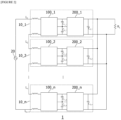
- FIG. 1 is a schematic view illustrating a configuration of a semiconductor transformer module 10 according to one embodiment of the present invention.
- FIG. 2 is a schematic view illustrating a configuration of a transformer 1 according to one embodiment of the present invention.
- the semiconductor transformer module 10 includes a semiconductor transformer circuit in which an AC-DC active front end (AFE) rectifier 100 and a dual active bridge (DAB) converter 200 are coupled.
- the semiconductor transformer module 10 may be one of a plurality of modules 10_1, 10_2,... and 10_n included in the transformer 1.
- the transformer 1 is a semiconductor transformer (solid state transformer (SST)) used for power.
- the semiconductor transformer 1 used for power may serve to divide power through a voltage variation function at branch points for power transmission, power distribution, and electrical distribution in a system.
- the semiconductor transformer 1 may have a reduced size and high efficiency as compared to existing power transformers which are heavy and bulky.
- a high frequency is a frequency higher than the commercial frequency (60Hz).
- a low frequency may be 60Hz or the like, and a high frequency may be 10 kHz or the like, but the present invention is not limited thereto.
- the semiconductor transformer 1 may be implemented as a series system and may include the semiconductor transformer modules 10_1, 10_2, ..., and 10_n which are a plurality of sub-systems connected in series with each other with respect to a power source 20, wherein n is a natural number of 2 or more.
- a first power line L 1 is provided between a first input terminal of the power source 20 and a first input terminal of a first semiconductor transformer module 10_1
- a second power line L 2 is provided between a second input terminal of the first semiconductor transformer module 10_1 and a first input terminal of a second semiconductor transformer module 10_2
- an n th power line L n is provided between a second input terminal of an (n-1) th semiconductor transformer module 10_n-1 and a first input terminal of an n th semiconductor transformer module 10_n
- an (n+1) th power line L n+1 is provided between a second input terminal of the n th semiconductor transformer module 10_n and a second input terminal of the power source 20.
- inductors are illustrated as being connected to the lines L 1 , L2, ..., Ln, and L n+1 , but the present invention is not limited thereto. That is, active elements (such as inductors) or passive elements (such as resistors) may be additionally connected to the lines L 1 , L2, ..., Ln, and L n+1 .
- first output terminals of the semiconductor transformer module 10_1, 10_2, ..., and 10_n are connected to a first terminal of a load R L
- second output terminals of the semiconductor transformer modules 10_1, 10_2, ..., and 10_n are connected to a second terminal of the load R L .
- each semiconductor transformer module 10_1, 10_2,... or 10_n performs a transforming function on the power distributed in series, and the transformed power is transmitted to the load R L .
- each of the semiconductor transformer modules 10_1, 10_2, ..., and 10_n may include the AFE rectifier 100 and the DAB converter 200 which are transformer circuits for a transforming function.
- a controller (not shown) for controlling such a transforming function may be included in the transformer 1.
- the semiconductor transformer 1 may include only one semiconductor transformer module 10.
- the second power line L 2 may be connected between a first input terminal of the semiconductor transformer module 10 and the second input terminal of the power source 20.
- the load R L shown in FIG. 2 may be a line such as a distribution line, a DC-AC converter, or various systems that perform specific functions using transformed DC power.
- the load R L may be a system including an inverter or a programmable logic controller (PLC) that controls the driving of an electric motor and may be a system for various functions related to measurement, communication, input, output, calculation, and the like, but the present invention is not limited thereto.
- PLC programmable logic controller
- an SST may be applied to a distribution system.
- Such SSTs may be classified into a non-modular SST, a semi-Modular SST, and a modular SST.
- the semiconductor transformer 1 according to the present invention may be a modular SST in which the semiconductor transformer modules 10_1, 10_2, ..., and 10_n are connected in series.
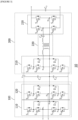
- FIG. 3 illustrates a detailed circuit (that is., a topology) of the semiconductor transformer module 10 according to one embodiment of the present invention.
- the AFE rectifier 100 and the DAB converter 200 may be connected in series, and DC link capacitors C 1 and C 2 may be connected in series therebetween.
- a first output terminal of the AFE rectifier 100 is connected to one end of a first DC link capacitor C 1 and a first input terminal of the DAB converter 200, and a second output terminal of the AFE rectifier 100 is connected to the other end of a second DC link capacitor C 2 and a second input terminal of the DAB converter 200.
- the other end of the first DC link capacitor C 1 and one end of the second DC link capacitor C 2 are connected, and a node N 2 is formed therebetween.
- a first input terminal of the AFE rectifier 100 to which any one line of the power source is connected is connected to a node N 1
- a second input terminal of the AFE rectifier 100 to which the other line of the power source is connected is connected to the node N 2 . That is, the node N 1 is connected to one of the lines L 1 , L2, ..., Ln, and L n+1
- the node N 2 is connected to another one of the lines L 1 , L2, ..., Ln, and L n+1 .
- the semiconductor transformer module 10 is a first module in the semiconductor transformer 1
- the node N 1 is connected to the line L 1
- the node N 2 is connected to the line L 2 .
- a DC link capacitor C 3 are connected to the first and second output terminals of the DAB converter 200, respectively.
- the first and second DC link capacitors C 1 and C 2 may be components included in the AFE rectifier 100, and the DC link capacitor C 3 may be a component included in the DAB converter 200.
- the AFE rectifier 100 actively controls low-frequency AC power output from the power source 20 and convert the low-frequency AC power into DC power.
- the AFE rectifier 100 has advantages of controlling a voltage of the DC link capacitors C 1 and C 2 (hereinafter referred to as "link voltage"), maintaining a constant DC link voltage, controlling a power factor of an input, and removing harmonic waves included in an input current.
- the AFE rectifier 100 may be a controllable rectifier in which an existing diode element is changed into a switch element such as an insulated gate bipolar transistor (IGBT) metal oxide silicon field effect transistor (MOSFET), may provide bidirectional power exchange between AC and DC, may regenerate reusable power to a main power source to reduce power costs, and may considerably lower a peak of a current using pulse width modulation (PWM) modulation.
- IGBT insulated gate bipolar transistor
- MOSFET metal oxide silicon field effect transistor
- the AFE rectifier 100 includes two full bridge legs 110 and 120 each having three levels, and first and second full bridge legs 110 and 120 form one full bridge.
- the first full bridge leg 110 includes four switch elements S 11 , S 12 , S 13 , and S 14 and two diodes D 11 and D 12 .
- the second full bridge 120 includes four switch elements S 21 , S 22 , S 23 , and S 24 and two diodes D 21 and D 22 .
- the AFE rectifier 100 has an advantage capable of minimizing the number of components such as switch elements at various rated voltages (for example, 13.2 kV in series).
- switch elements and passive elements with different ratings should be used, which causes a problem in an increase in manufacturing costs.
- switch elements having the same rating may be used, thereby lowering manufacturing costs.
- the switch elements S 11 , S 12 , S 13 , S 14 , S 21 , S 22 , S 23 , and S 24 of the first and second full bridge legs 110 and 120 is determined according to a control signal of the controller (not shown).
- the switch elements S 11 , S 12 , S 13 , S 14 , S 21 , S 22 , S 23 , and S 24 may be power switch elements such as IGBTs, MOSFETs, or gate turn-off thyristors (GTOs).
- Each of the switch elements S 11 , S 12 , S 13 , S 14 , S 21 , S 22 , S 23 , and S 24 includes three electrodes.
- one of the three electrodes is a gate G
- another one for example, one end
- still another one that is, the other end
- the switch elements S 11 , S 12 , S 13 , S 14 , S 21 , S 22 , S 23 , and S 24 are the MOSFETs
- one of the first electrode and the second electrode may be a source S
- the other one may be a drain D.
- a control signal line of the controller (not shown) may be connected to the gate G, and an additional diode may be connected between the first electrode and the second electrode.
- the switch element S 11 , S 12 , S 13 , and S 14 are connected in series. That is, the other end of the switch element S 11 and one end of the switch element S 12 are connected to form a node N 3 , the other end of the switch element S 12 and one end of the switch element S 13 are connected to form the node N 1 , and the other end of the switch element S 13 and one end of the switch element S 14 are connected to form a node N 4 .
- one end of the switch element S 11 may be connected to one end of the first DC link capacitor C 1 to serve as the first output terminal of the AFE rectifier 100, and the other end of the switch element S 14 may be connected to the other end of the second DC link capacitor C 2 to serve as the second output terminal of the AFE rectifier 100.
- the diodes D 11 and D 12 are also connected in series. That is, the other end of the diode D 11 and one end of the diode D 12 are connected to form a node N 5 . In this case, one end of the diode D 11 is connected to the node N 3 , and the other end of the diode D 12 is connected to the node N 4 .
- the switch elements S 21 , S 22 , S 23 , and S 24 are connected in series. That is, the other end of the switch element S 21 and one end of the switch element S 22 are connected to form a node N 6 , the other end of the switch element S 22 and one end of the switch element S 23 are connected to form the node N 2 , and the other end of the switch element S 23 and one end of the switch element S 24 are connected to form a node N 7 .
- one end of the switch element S 21 may be connected to one end of the first DC link capacitor C 1 to serve as the first output terminal of the AFE rectifier 100, and the other end of the switch element S 24 may be connected to one end of a capacitor C 4 to serve as the second output terminal of the AFE rectifier 100.
- the diodes D 21 and D 22 are also connected in series. That is, the other end of the diode D 21 and one end of the diode D 22 are connected to each other and connected to the node N 5 . In this case, one end of the diode D 21 is connected to the node N 6 , and the other end of the diode D 22 is connected to the node N 7 .
- the first and second full bridge legs 110 and 120 each have three levels. That is, in the first full bridge leg 110, a first level corresponds to a state in which the switch elements S 11 and S 12 are turned on and the switch elements S 13 and S 14 are turned off, a second level corresponds to a state in which the switch elements S 11 and S 12 are turned off and the switch elements S 13 and S 14 are turned on, and a third level corresponds to a state in which the switch elements S 11 and S 14 are turned on.
- a first level corresponds to a state in which the switch elements S 21 and S 22 are turned on and the switch elements S 23 and S 24 are turned off
- a second level corresponds to a state in which the switch elements S 21 and S 22 are turned off and the switch elements S 23 and S 24 are turned on
- a third level corresponds to a state in which the switch elements S 21 and S 24 are turned on. Accordingly, a total of five levels may be output by the first and second full bridge legs 110 and 120.
- a voltage between the first output terminal and the second output terminal of the AFE rectifier 100 (that is, a voltage between one end of the first DC link capacitor C 1 and the other end of the second DC link capacitor C 2 ) is assumed to be V DC
- a voltage between the node N 1 and the node N 2 may exhibit a total of five levels of V DC , V DC /2, 0 V, - V DC /2, and -V DC .
- the DAB converter 200 may operate as a DC-DC converter and may perform a first operation of converting a DC converted in the AFE rectifier 100 into a high-frequency AC, a second operation of transforming the converted high-frequency AC into a high-frequency and low-voltage AC, and a third operation of converting the high-frequency and low-voltage AC into low-voltage DC.
- the DAB converter 200 may be one of DC-DC converters. Unlike bidirectional resonant converters such as capacitor-inductor-inductor-capacitor (CLLC) converters, the DAB converter 200 has an advantage in that a direction change of a load current is smooth, and a power direction is easily controlled by a phase shift.
- CLLC capacitor-inductor-inductor-capacitor
- the DAB converter 200 includes a half bridge 210 that has three levels and performs the first operation, a transformation portion 220 (also referred to as a transformation unit) that performs the second operation, and a third full bridge 230 that has two levels and performs the third operation.
- the half bridge 210 includes four switch elements S 31 , S 32 , S 33 , and S 34 and two diodes D 31 and D 32 .
- the transformation portion 220 includes a primary side and a secondary side.
- the full bridge 230 includes four switch elements S 41 , S 42 , S 43 , and S 44 .
- Each of the switch elements S 31 , S 32 , S 33 , S 34 , S 41 , S 42 , S 43 , and S 44 includes three electrodes.
- one of the three electrodes is a gate G
- another one for example, one end
- still another one that is, the other end
- the switch elements S 31 , S 32 , S 33 , S 34 , S 41 , S 42 , S 43 , and S 44 are MOSFETs
- one of the first electrode and the second electrode may be a source S
- the other one may be a drain D.
- control signal line of the controller (not shown) may be connected to the gate G, and an additional diode may be connected between the first electrode and the second electrode.
- the switch element S 31 , S 32 , S 33 , and S 34 are connected in series. That is, the other end of the switch element S 31 and one end of the switch element S 32 are connected to form a node N 9 , the other end of the switch element S 32 and one end of the switch element S 33 are connected to form a node N 10 , and the other end of the switch element S 33 and one end of the switch element S 34 are connected to form a node N 11 .
- one end of the switch element S 31 may be connected to one end of the first DC link capacitor C 1 to serve as the first input terminal of the DAB converter 200, and the other end of the switch element S 34 may be connected to the other end of the second DC link capacitor C 2 to serve as the second input terminal of the AFE rectifier 100.
- the diodes D 31 and D 32 are also connected in series. That is, the other end of the diode D 31 and one end of the diode D 32 are connected to each other and connected to the node N 5 . In this case, one end of the diode D 31 is connected to the node N 9 , and the other end of the diode D 32 is connected to the node N 11 .
- a first output terminal of the half bridge 210 connected to a first input terminal of the transformation portion 220 is the node N 10
- a second output terminal of the half bridge 210 connected to a second input terminal of the transformation portion 220 is the node N 5 .
- the half bridge 210 has three levels. That is, in the half bridge 210, a first level corresponds to a state in which the switch elements S 31 and S 32 are turned on and the switch elements S 33 and S 34 are turned off, a second level corresponds to a state in which the switch elements S 32 and S 33 are turned on and the switch elements S 31 and S 34 are turned off, and a third level corresponds to a state in which the switch elements S 31 and S 32 are turned off and the switch elements S 33 and S 34 are turned on.
- V DC /2 may be applied at the first level
- 0 V may be applied at the second level
- -V DC /2 may be applied at the third level.
- a first process of sequentially changing levels from the first level to the third level, and then, a second process of sequentially changing levels from the third level to the first level may be repeatedly performed to perform a first operation of converting DC converted in the AFE rectifier 100 into high-frequency AC.
- the primary side and the secondary side of the transformation portion 220 may each include coils having various windings. In this case, it may be preferable that a number of turns of coils of the primary side be greater than a number of coil turns of coils of the secondary side. That is, a converted high-frequency AC input to the primary side is transformed into high-frequency and low-voltage AC according to a relationship between the number of turns in the primary side and the secondary side.
- a first input terminal of the primary side serves as the first input terminal of the transformation portion 220 and is connected to the node N 10 which is the first output terminal of the half bridge 210.
- a second input terminal of the primary side serves as the second input terminal of the transformation portion 220 and is connected to the node N 5 which is the second output terminal of the half bridge 210.
- an active element such as an inductor
- a passive element such as a resistor
- a first output terminal of the secondary side serves as a first output terminal of the transformation portion 220 and is connected to a node N 12 which is a first input terminal of the third full bridge 230.
- a second output terminal of the secondary side serves as a second output terminal of the transformation portion 220 and is connected to a node N 13 which is a second input terminal of the third full bridge 230.
- an active element such as an inductor
- a passive element such as a resistor
- the capacitor C 4 for a DC blocking function that is, a function of removing a DC component from transformed low-voltage AC
- the third full bridge 230 includes four switch elements S 41 , S 42 , S 43 , and S 44 . Whether to turn on or off the switch elements S 41 , S 42 , S 43 , and S 44 of the third full bridge 230 is determined according to a control signal of the controller (not shown).
- the switch elements S 41 , S 42 , S 43 , and S 44 may be power switch elements such as IGBTs, MOSFETs, or GTOs.
- Each of the switch elements S 41 , S 42 , S 43 , and S 44 includes three electrodes.
- one of the three electrodes is a gate G
- another one (for example, one end) is a first electrode
- still another one (that is, the other end) is a second electrode.
- the switch elements S 41 , S 42 , S 43 , and S 44 are the MOSFETs
- one of the first and second electrodes may be a source S
- the other may be a drain D.
- a control signal line of the controller (not shown) may be connected to the gate G, and an additional diode may be connected between the first electrode and the second electrode.
- the switch elements S 41 and S 42 connected to each other in series form one full bridge leg, and the switch elements S 43 and S 44 connected to each other in series form another full bridge leg. That is, the other end of the switch element S 41 and one end of the switch element S 42 are connected to form the node N 12 , and the other end of the switch element S 43 and one end of the switch element S 44 are connected to form the node N 13 .
- one end of the switch element S 41 and one end of the switch element S 43 may be connected to one end of the DC link capacitor C 3 to serve as the first output terminal of the DAB converter 200, and the other ends of the switch elements S 42 and S 44 may be connected to the other end of the DC link capacitor C 3 to serve as the second output terminal of the DAB converter 200.
- one end of the DC link capacitor C 3 may serve as a first output terminal of the semiconductor transformer module 10 to be connected to a first terminal of the load R L
- the other end of the DC link capacitor C 3 may serve as a second output terminal of the semiconductor transformer module 10 to be connected to a second terminal of the load R L .
- the third full bridge 230 has two levels. That is, in the third full bridge 230, a first level corresponds to a state in which the switch elements S 41 and S 44 are turned on and the switch elements S 42 and S 43 are turned off, and a second level corresponds to a state in which the switch elements S 41 and S 44 are turned off and the switch elements S 42 and S 43 are turned on. Processes of the first level and second level may be repeatedly performed to perform a third operation of converting high-frequency and low-voltage AC converted in the transformation portion 220 into DC, and according to the third operation, DC applied to the DC link capacitor C 3 may be transmitted to the load R L .
- the present invention configured as described above, there is an advantage in that the number of switch elements in a power semiconductor transformer can be reduced to reduce manufacturing costs.
- switch elements with the same rating can be used in all AFE rectifiers to reduce manufacturing costs.
- the present invention relates to a power semiconductor transformer module and a transformer using the same.
- a power semiconductor transformer module implemented in a topology capable of minimizing the number of switch elements to reduce manufacturing costs, and a transformer using the same.
- the present invention has industrial applicability.
Landscapes
- Engineering & Computer Science (AREA)
- Power Engineering (AREA)
- Dc-Dc Converters (AREA)
Applications Claiming Priority (2)
| Application Number | Priority Date | Filing Date | Title |
|---|---|---|---|
| KR1020220012203A KR102594689B1 (ko) | 2022-01-27 | 2022-01-27 | 전력용 반도체 변압기 모듈 및 이를 이용한 변압기 |
| PCT/KR2023/001157 WO2023146282A1 (ko) | 2022-01-27 | 2023-01-26 | 전력용 반도체 변압기 모듈 및 이를 이용한 변압기 |
Publications (2)
| Publication Number | Publication Date |
|---|---|
| EP4472053A1 true EP4472053A1 (de) | 2024-12-04 |
| EP4472053A4 EP4472053A4 (de) | 2025-11-19 |
Family
ID=87472074
Family Applications (1)
| Application Number | Title | Priority Date | Filing Date |
|---|---|---|---|
| EP23747323.6A Pending EP4472053A4 (de) | 2022-01-27 | 2023-01-26 | Leistungsfestkörpertransformatormodul und transformator damit |
Country Status (5)
| Country | Link |
|---|---|
| US (1) | US20250226754A1 (de) |
| EP (1) | EP4472053A4 (de) |
| KR (1) | KR102594689B1 (de) |
| CN (1) | CN118435510A (de) |
| WO (1) | WO2023146282A1 (de) |
Family Cites Families (9)
| Publication number | Priority date | Publication date | Assignee | Title |
|---|---|---|---|---|
| KR101303002B1 (ko) * | 2012-08-17 | 2013-09-03 | 한국전력공사 | 전력용 반도체를 이용한 직렬 연결형 전력 변환 장치와 그 방법 |
| KR101769335B1 (ko) * | 2015-10-22 | 2017-08-18 | 월드탑텍(주) | 멀티 토플러지를 이용한 dc/dc 컨버터 |
| JP6711449B2 (ja) * | 2017-03-14 | 2020-06-17 | 株式会社村田製作所 | Dc−dcコンバータ |
| KR101817903B1 (ko) * | 2017-07-19 | 2018-01-11 | 재단법인경북테크노파크 | 전기 자동차용 고강압 직류/직류 전력변환기 |
| CN109742968B (zh) * | 2019-01-31 | 2020-12-04 | 上海交通大学 | 二极管箝位混合三电平双有源全桥变流器及其控制方法 |
| KR102181321B1 (ko) * | 2019-11-27 | 2020-11-23 | 한국전기연구원 | 전력변환장치 |
| KR102500741B1 (ko) * | 2020-05-25 | 2023-02-20 | 한밭대학교 산학협력단 | 전기자동차용 obc 및 ldc 결합 일체형 전력 변환 회로 |
| CN115133761B (zh) * | 2021-03-26 | 2025-07-15 | 台达电子企业管理(上海)有限公司 | Pfc电路及其控制方法,功率变换装置 |
| CN115589139A (zh) * | 2021-07-05 | 2023-01-10 | 台达电子企业管理(上海)有限公司 | 电源转换装置 |
-
2022
- 2022-01-27 KR KR1020220012203A patent/KR102594689B1/ko active Active
-
2023
- 2023-01-26 WO PCT/KR2023/001157 patent/WO2023146282A1/ko not_active Ceased
- 2023-01-26 US US18/727,784 patent/US20250226754A1/en active Pending
- 2023-01-26 EP EP23747323.6A patent/EP4472053A4/de active Pending
- 2023-01-26 CN CN202380015504.8A patent/CN118435510A/zh active Pending
Also Published As
| Publication number | Publication date |
|---|---|
| CN118435510A (zh) | 2024-08-02 |
| US20250226754A1 (en) | 2025-07-10 |
| KR20230115576A (ko) | 2023-08-03 |
| WO2023146282A1 (ko) | 2023-08-03 |
| KR102594689B1 (ko) | 2023-10-25 |
| EP4472053A4 (de) | 2025-11-19 |
Similar Documents
| Publication | Publication Date | Title |
|---|---|---|
| US11088625B1 (en) | Three-phase CLLC bidirectional DC-DC converter and a method for controlling the same | |
| US8743575B2 (en) | Switch mode pulse width modulated DC-DC converter with multiple power transformers | |
| CN113261191A (zh) | 双向多端口功率转换系统及方法 | |
| US10432101B2 (en) | Power conversion apparatus | |
| KR102601772B1 (ko) | 차량-측면 충전 디바이스 | |
| US11296607B2 (en) | DC-DC converter | |
| US10873254B2 (en) | Electrical circuit for zero-voltage soft-switching in DC-DC converter under all load conditions | |
| EP4113813A1 (de) | Leistungselektronisches gerät zum umwandeln von wechselstrom in gleichstrom | |
| Tuan et al. | Output Power Characteristics of Unidirectional Secondary-Resonant Single-Active-Bridge DC-DC Converter using Pulse Width Control | |
| EP3610567B1 (de) | Effiziente umwandlung von elektrischem strom | |
| CN119519365A (zh) | 一种单桥臂电力电子变压器拓扑结构及方法 | |
| EP4472051A1 (de) | Halbleitertransformator und modulare hochspannungsleistungsvorrichtung | |
| US12246609B2 (en) | Charging device and method for operating the charging device | |
| Rehlaender et al. | Dual interleaved 3.6 kW LLC converter operating in half-bridge, full-bridge and phase-shift mode as a single-stage architecture of an automotive on-board DC-DC converter | |
| US20250167685A1 (en) | Power supply device using dc link voltage of high-voltage unit of semiconductor transformer | |
| EP4472053A1 (de) | Leistungsfestkörpertransformatormodul und transformator damit | |
| EP4300798A1 (de) | Resonanzleistungswandler | |
| KR20240021120A (ko) | Ac 배터리에 통합된 직류-직류 변환기를 위한 방법및 회로 | |
| CN117897883A (zh) | 用于感应式电力传输的无线电力传输设备和用于操作该电力传输设备以支持零电压切换的方法 | |
| CA3186203A1 (en) | Dc to dc boost converter | |
| KR20230130865A (ko) | 반도체 변압기 및 그 초기 기동 제어방법 | |
| KR102952579B1 (ko) | 출력 절체기능을 구비한 절연형 양방향 충전시스템 | |
| WO2024082211A1 (en) | Dc-to-dc power converter | |
| Mohseni et al. | Novel Concept of Universal AC/DC-DC Onboard Battery Charger for Electric Vehicles | |
| WO2025218882A1 (en) | Series-connected interleaved phase-shifted full-bridges with reduced number of output inductors and a method for performing dc-dc conversion |
Legal Events
| Date | Code | Title | Description |
|---|---|---|---|
| STAA | Information on the status of an ep patent application or granted ep patent |
Free format text: STATUS: THE INTERNATIONAL PUBLICATION HAS BEEN MADE |
|
| PUAI | Public reference made under article 153(3) epc to a published international application that has entered the european phase |
Free format text: ORIGINAL CODE: 0009012 |
|
| STAA | Information on the status of an ep patent application or granted ep patent |
Free format text: STATUS: REQUEST FOR EXAMINATION WAS MADE |
|
| 17P | Request for examination filed |
Effective date: 20240627 |
|
| AK | Designated contracting states |
Kind code of ref document: A1 Designated state(s): AL AT BE BG CH CY CZ DE DK EE ES FI FR GB GR HR HU IE IS IT LI LT LU LV MC ME MK MT NL NO PL PT RO RS SE SI SK SM TR |
|
| DAV | Request for validation of the european patent (deleted) | ||
| DAX | Request for extension of the european patent (deleted) | ||
| A4 | Supplementary search report drawn up and despatched |
Effective date: 20251021 |
|
| RIC1 | Information provided on ipc code assigned before grant |
Ipc: H02M 7/219 20060101AFI20251015BHEP Ipc: H02M 3/335 20060101ALI20251015BHEP Ipc: H02M 7/487 20070101ALI20251015BHEP |