EP4471858A1 - Display device and tiled display device comprising same - Google Patents
Display device and tiled display device comprising same Download PDFInfo
- Publication number
- EP4471858A1 EP4471858A1 EP23747246.9A EP23747246A EP4471858A1 EP 4471858 A1 EP4471858 A1 EP 4471858A1 EP 23747246 A EP23747246 A EP 23747246A EP 4471858 A1 EP4471858 A1 EP 4471858A1
- Authority
- EP
- European Patent Office
- Prior art keywords
- pad
- area
- substrate
- display device
- disposed
- Prior art date
- Legal status (The legal status is an assumption and is not a legal conclusion. Google has not performed a legal analysis and makes no representation as to the accuracy of the status listed.)
- Pending
Links
Images






Classifications
-
- H—ELECTRICITY
- H10—SEMICONDUCTOR DEVICES; ELECTRIC SOLID-STATE DEVICES NOT OTHERWISE PROVIDED FOR
- H10H—INORGANIC LIGHT-EMITTING SEMICONDUCTOR DEVICES HAVING POTENTIAL BARRIERS
- H10H20/00—Individual inorganic light-emitting semiconductor devices having potential barriers, e.g. light-emitting diodes [LED]
- H10H20/80—Constructional details
- H10H20/85—Packages
- H10H20/857—Interconnections, e.g. lead-frames, bond wires or solder balls
-
- G—PHYSICS
- G09—EDUCATION; CRYPTOGRAPHY; DISPLAY; ADVERTISING; SEALS
- G09F—DISPLAYING; ADVERTISING; SIGNS; LABELS OR NAME-PLATES; SEALS
- G09F9/00—Indicating arrangements for variable information in which the information is built-up on a support by selection or combination of individual elements
- G09F9/30—Indicating arrangements for variable information in which the information is built-up on a support by selection or combination of individual elements in which the desired character or characters are formed by combining individual elements
- G09F9/302—Indicating arrangements for variable information in which the information is built-up on a support by selection or combination of individual elements in which the desired character or characters are formed by combining individual elements characterised by the form or geometrical disposition of the individual elements
-
- G—PHYSICS
- G09—EDUCATION; CRYPTOGRAPHY; DISPLAY; ADVERTISING; SEALS
- G09F—DISPLAYING; ADVERTISING; SIGNS; LABELS OR NAME-PLATES; SEALS
- G09F9/00—Indicating arrangements for variable information in which the information is built-up on a support by selection or combination of individual elements
- G09F9/30—Indicating arrangements for variable information in which the information is built-up on a support by selection or combination of individual elements in which the desired character or characters are formed by combining individual elements
- G09F9/302—Indicating arrangements for variable information in which the information is built-up on a support by selection or combination of individual elements in which the desired character or characters are formed by combining individual elements characterised by the form or geometrical disposition of the individual elements
- G09F9/3026—Video wall, i.e. stackable semiconductor matrix display modules
-
- G—PHYSICS
- G09—EDUCATION; CRYPTOGRAPHY; DISPLAY; ADVERTISING; SEALS
- G09F—DISPLAYING; ADVERTISING; SIGNS; LABELS OR NAME-PLATES; SEALS
- G09F9/00—Indicating arrangements for variable information in which the information is built-up on a support by selection or combination of individual elements
- G09F9/30—Indicating arrangements for variable information in which the information is built-up on a support by selection or combination of individual elements in which the desired character or characters are formed by combining individual elements
- G09F9/33—Indicating arrangements for variable information in which the information is built-up on a support by selection or combination of individual elements in which the desired character or characters are formed by combining individual elements being semiconductor devices, e.g. diodes
-
- H—ELECTRICITY
- H05—ELECTRIC TECHNIQUES NOT OTHERWISE PROVIDED FOR
- H05K—PRINTED CIRCUITS; CASINGS OR CONSTRUCTIONAL DETAILS OF ELECTRIC APPARATUS; MANUFACTURE OF ASSEMBLAGES OF ELECTRICAL COMPONENTS
- H05K3/00—Apparatus or processes for manufacturing printed circuits
- H05K3/36—Assembling printed circuits with other printed circuits
- H05K3/361—Assembling flexible printed circuits with other printed circuits
-
- H—ELECTRICITY
- H10—SEMICONDUCTOR DEVICES; ELECTRIC SOLID-STATE DEVICES NOT OTHERWISE PROVIDED FOR
- H10D—INORGANIC ELECTRIC SEMICONDUCTOR DEVICES
- H10D86/00—Integrated devices formed in or on insulating or conducting substrates, e.g. formed in silicon-on-insulator [SOI] substrates or on stainless steel or glass substrates
- H10D86/40—Integrated devices formed in or on insulating or conducting substrates, e.g. formed in silicon-on-insulator [SOI] substrates or on stainless steel or glass substrates characterised by multiple TFTs
- H10D86/441—Interconnections, e.g. scanning lines
-
- H—ELECTRICITY
- H10—SEMICONDUCTOR DEVICES; ELECTRIC SOLID-STATE DEVICES NOT OTHERWISE PROVIDED FOR
- H10H—INORGANIC LIGHT-EMITTING SEMICONDUCTOR DEVICES HAVING POTENTIAL BARRIERS
- H10H29/00—Integrated devices, or assemblies of multiple devices, comprising at least one light-emitting semiconductor element covered by group H10H20/00
- H10H29/10—Integrated devices comprising at least one light-emitting semiconductor component covered by group H10H20/00
- H10H29/14—Integrated devices comprising at least one light-emitting semiconductor component covered by group H10H20/00 comprising multiple light-emitting semiconductor components
- H10H29/142—Two-dimensional arrangements, e.g. asymmetric LED layout
-
- H—ELECTRICITY
- H10—SEMICONDUCTOR DEVICES; ELECTRIC SOLID-STATE DEVICES NOT OTHERWISE PROVIDED FOR
- H10K—ORGANIC ELECTRIC SOLID-STATE DEVICES
- H10K59/00—Integrated devices, or assemblies of multiple devices, comprising at least one organic light-emitting element covered by group H10K50/00
- H10K59/10—OLED displays
- H10K59/18—Tiled displays
-
- H—ELECTRICITY
- H05—ELECTRIC TECHNIQUES NOT OTHERWISE PROVIDED FOR
- H05K—PRINTED CIRCUITS; CASINGS OR CONSTRUCTIONAL DETAILS OF ELECTRIC APPARATUS; MANUFACTURE OF ASSEMBLAGES OF ELECTRICAL COMPONENTS
- H05K1/00—Printed circuits
- H05K1/02—Details
- H05K1/11—Printed elements for providing electric connections to or between printed circuits
- H05K1/118—Printed elements for providing electric connections to or between printed circuits specially for flexible printed circuits, e.g. using folded portions
-
- H—ELECTRICITY
- H05—ELECTRIC TECHNIQUES NOT OTHERWISE PROVIDED FOR
- H05K—PRINTED CIRCUITS; CASINGS OR CONSTRUCTIONAL DETAILS OF ELECTRIC APPARATUS; MANUFACTURE OF ASSEMBLAGES OF ELECTRICAL COMPONENTS
- H05K2201/00—Indexing scheme relating to printed circuits covered by H05K1/00
- H05K2201/10—Details of components or other objects attached to or integrated in a printed circuit board
- H05K2201/10007—Types of components
- H05K2201/10128—Display
-
- H—ELECTRICITY
- H10—SEMICONDUCTOR DEVICES; ELECTRIC SOLID-STATE DEVICES NOT OTHERWISE PROVIDED FOR
- H10K—ORGANIC ELECTRIC SOLID-STATE DEVICES
- H10K59/00—Integrated devices, or assemblies of multiple devices, comprising at least one organic light-emitting element covered by group H10K50/00
- H10K59/10—OLED displays
-
- H—ELECTRICITY
- H10—SEMICONDUCTOR DEVICES; ELECTRIC SOLID-STATE DEVICES NOT OTHERWISE PROVIDED FOR
- H10W—GENERIC PACKAGES, INTERCONNECTIONS, CONNECTORS OR OTHER CONSTRUCTIONAL DETAILS OF DEVICES COVERED BY CLASS H10
- H10W90/00—Package configurations
Definitions
- the present disclosure relates to a display device and a tiled display device including the same.
- a display device is a device for displaying a moving image or a still image.
- the display device may be used as a display screen of various products such as televisions, laptop computers, monitors, billboards and the Internet of Things (IoT) as well as portable electronic devices such as mobile phones, smart phones, tablet personal computers (tablet PCs), smart watches, watch phones, mobile communication terminals, electronic notebooks, electronic books, portable multimedia players (PMPs), navigation systems, and ultra mobile personal computers (UMPCs).
- IoT Internet of Things
- portable electronic devices such as mobile phones, smart phones, tablet personal computers (tablet PCs), smart watches, watch phones, mobile communication terminals, electronic notebooks, electronic books, portable multimedia players (PMPs), navigation systems, and ultra mobile personal computers (UMPCs).
- a printed circuit board including a driver circuit, a plurality of signal wires electrically connecting the light emitting elements, and a plurality of lead wires connected to the signal wires.
- the display device includes a display area where an image is displayed and a portion (e.g., bezel) surrounding the display area, where an image is not displayed.
- the signal and lead wires may be bonded to the side surface of the display device e.g., by a side-bonding method.
- aspects of the present disclosure also provide a tiled display device in which delamination of a driving pad caused by a test pad is prevented.
- An embodiment of a display device comprises a first substrate comprising a display area comprising pixels, a pad area comprising a plurality of pads and a side wiring area located adjacent to the display area; and a printed circuit film attached to the pad area located on a back surface of the first substrate, wherein: a plurality of pads of the first substrate are disposed in the pad area, the plurality of pads comprise a plurality of first pads configured to connect the printed circuit film to the pixels and a second pad disposed between the adjacent first pads, the display device further comprises a connection portion that electrically connects the first pad and the second pad to each other, the first pad comprises a first-first pad located on a front surface of the first substrate and a first-second pad located on the back surface of the first substrate, and the display device further comprises side wirings disposed in the side wiring area and electrically connect the first-first pad and the first-second pad to each other.
- An embodiment of a display device comprises a first substrate comprising a display area comprising pixels, a pad area comprising a plurality of pads and located adjacent to the display area and a side wiring area located adjacent to the display area; a second substrate opposite to the first substrate; and a printed circuit film attached to the pad area located on a back surface of the first substrate, wherein: a plurality of pads of the first substrate are disposed in the pad area, the plurality of pads comprise a plurality of first pads that electrically connect the printed circuit film to the pixels, and a second pad disposed between the adjacent first pads and comprising a plurality of patterns, the display device further comprises a connection portion configured to connect the first pad and the plurality of patterns of the second pad to each other, the first pad comprises a first-first pad located on a front surface of the first substrate and a first-second pad located on the back surface of the first substrate, and the display device further comprises side wirings that are disposed in the side wiring area and that electrically connect the first-first pad and the first-second pad
- An embodiment of a tiled display device comprises a plurality of first substrates each comprising a display area comprising pixels, a pad area comprising a plurality of pads and located adjacent to the display area, and a side wiring area comprising side wirings and located adjacent to the display area; and a printed circuit film attached to the pad area located on a back surface of the first substrate, wherein: the first substrate comprises: a base substrate, a first conductive layer comprising a connection portion on the base substrate, an insulating layer on the first conductive layer, a second conductive layer comprising a first lower pad portion on the conductive layer and a second lower pad portion, and a third conductive layer comprising a first upper pad portion overlapping the first lower pad portion on the second conductive layer in a plan view and a second upper pad portion overlapping the second lower pad portion in a plan view, wherein: the pads comprise a plurality of first pads that electrically connect the printed circuit film to the pixels, and a second pad disposed between the adjacent first pads, the first pad comprises
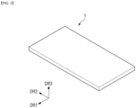
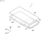
- FIG. 1 is a perspective view of a display device according to an embodiment of the present disclosure.
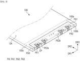
- FIG. 2 is a detailed perspective view of the display device shown in FIG. 1 .
- a display device 1 may be a subminiature light emitting diode display device (micro or nano light emitting diode display device) including a subminiature light emitting diode (micro or nano light emitting diode) as a light emitting element LE, but embodiments of the present disclosure are not limited thereto.
- a first direction DR1 refers to a horizontal direction of the display device 1
- a second direction DR2 refers to a vertical direction of the display device 1
- a third direction DR3 refers to a thickness direction of the display device 1.
- the term “right side” denotes one side in the first direction DR1
- the term “left side” denotes the other side in the first direction DR1
- the term “upper side” denotes one side in the second direction DR2
- the term “lower side” denotes the other side in the second direction DR2.
- the term “upper portion” denotes one side in the third direction DR3
- the term “lower portion” denotes the other side in the third direction DR3.
- the display device 1 may include a first substrate 100, a printed circuit film 400, and a main circuit board 500.
- the display device 1 may further include various elements disposed on the first substrate 100.
- a micro light emitting diode may be used as the display device 1.
- a micro LED may be used as the display device 1.
- the present disclosure is not limited thereto, and different types of display device, such as an organic light emitting display (OLED), a liquid crystal display (LCD), a quantum dot organic light emitting display, a quantum dot liquid crystal display, a quantum nano light emitting display, and the like, may be used as the display device.
- the various elements of the first substrate 100 may include a plurality of insulating layers, a plurality of conductive layers, at least one thin film transistor, and a light emitting element electrically connected to the at least one thin film transistor.
- the first substrate 100 may include a base substrate, a thin film transistor layer including the at least one thin film transistor, a wavelength conversion layer including at least one wavelength conversion pattern, and a color filter layer including at least one color filter.
- the first substrate 100 may include a base substrate.
- the base substrate of the first substrate 100 may include a rigid material, such as glass or quartz.
- the display device 1 may have a rectangular shape with right-angled corners in plan view.
- the display device 1 may have long sides and short sides in plan view.
- the short side of the display device 1 may be a side extending in the first direction DR1.
- the long side of the display device 1 may be a side extending in the second direction DR2.
- the first substrate 100 may include a display area DA.
- the display area DA of the first substrate 100 may include a plurality of pixels arranged thereon.
- Each of the pixels may include at least one thin film transistor and a light emitting element.
- the pad area PA may be attached to the printed circuit film 400.
- One end of the printed circuit film 400 may be attached to the pad area PA and the other end of the printed circuit film 400 may be attached to the main circuit board 500.
- the first pad PE1 may be disposed over the first to third pad areas PA1 to PA3.
- the second pad PE2 may be disposed in the first pad area PA1 and the third pad area PA3, but may not be disposed in the second pad area PA2.
- the connection portion CP may be disposed in the first pad area PA1 and the third pad area PA3, but may not be disposed in the second pad area PA2.
- the first pad PE1, the second pad PE2, and the connection portion CP will be described in further detail with reference to FIGS. 7 to 9 .
- Each of the display devices 1 is described above with reference to FIGS. 1 to 3 , and thus redundant descriptions thereof will be omitted.
- the sealing area may have a shape of a rectangle frame arranged to run along the edges of the first and second substrates 100 and 300.
- FIG. 14 is a perspective view illustrating a pad area and a side wiring area of a first substrate of a display device according to still another embodiment of the present disclosure.
- FIG. 15 is a side view of the first substrate shown in FIG. 14 .
- a first substrate 100_2 of a display device differs from the first substrate 100 of FIG. 3 in that the first substrate 100_2 does not include a second pad area PA2 and a side wiring area SPA is disposed in an area that corresponds to the second pad area PA2.
- the side wiring area SPA may be disposed between a first pad area PA1 and a third pad area PA3 and connect the first pad area PA1 to the third pad area PA3.
- the first pad PE1 is disposed in the first pad area PA1 and the third pad area PA3, and may not be disposed in the side wiring area SPA.
- a second pad PE2 may be disposed in the first pad area PA1 and the third pad area PA3, and may not be disposed in the side wiring area SPA.
- a connection portion CP may be disposed in the first pad area PA1 and the third pad area PA3, and may not be disposed in the side wiring area SPA.
- the first pad PE1 may include a first-first pad PE1a located in the first pad area PA1 and a first-third pad PE1c located in the third pad area PA3.
- a side wiring SPE may be disposed between the first-first pad PE1a and the first-third pad PE1c. An end of the side wiring SPE may be electrically connected to the first-first pad PE1a and another end of the side wiring SPE may be electrically connected to the first-third pad PE1c.
- the first-first pad PE1a and the side wiring SPE may be electrically connected (e.g., directly connected) to each other, and the side wiring SPE and the first-third pad PE1c may be electrically connected (e.g., directly connected) to each other.
- the second pad PE2 may include a second-first pad PE2a located in the first pad area PA1 and a second-second pad PE2b located in the third pad area PA3.
Landscapes
- Engineering & Computer Science (AREA)
- Physics & Mathematics (AREA)
- General Physics & Mathematics (AREA)
- Theoretical Computer Science (AREA)
- Multimedia (AREA)
- Manufacturing & Machinery (AREA)
- Microelectronics & Electronic Packaging (AREA)
- Devices For Indicating Variable Information By Combining Individual Elements (AREA)
- Liquid Crystal (AREA)
- Electroluminescent Light Sources (AREA)
- Led Device Packages (AREA)
Abstract
Description
- The present disclosure relates to a display device and a tiled display device including the same.
- A display device is a device for displaying a moving image or a still image. The display device may be used as a display screen of various products such as televisions, laptop computers, monitors, billboards and the Internet of Things (IoT) as well as portable electronic devices such as mobile phones, smart phones, tablet personal computers (tablet PCs), smart watches, watch phones, mobile communication terminals, electronic notebooks, electronic books, portable multimedia players (PMPs), navigation systems, and ultra mobile personal computers (UMPCs).
- In order to drive light emitting elements of the display device, there is a need of a printed circuit board including a driver circuit, a plurality of signal wires electrically connecting the light emitting elements, and a plurality of lead wires connected to the signal wires. The display device includes a display area where an image is displayed and a portion (e.g., bezel) surrounding the display area, where an image is not displayed. In order to implement a bezel-less design, the signal and lead wires may be bonded to the side surface of the display device e.g., by a side-bonding method.
- Aspects of the present disclosure provide a display device in which delamination of a driving pad caused by a test pad is prevented.
- Aspects of the present disclosure also provide a tiled display device in which delamination of a driving pad caused by a test pad is prevented.
- However, aspects of the present disclosure are not restricted to those set forth herein. The above and other aspects of the present disclosure will become more apparent to one of ordinary skill in the art to which the present disclosure pertains by referencing the detailed description of the present disclosure given below.
- An embodiment of a display device comprises a first substrate comprising a display area comprising pixels, a pad area comprising a plurality of pads and a side wiring area located adjacent to the display area; and a printed circuit film attached to the pad area located on a back surface of the first substrate, wherein: a plurality of pads of the first substrate are disposed in the pad area, the plurality of pads comprise a plurality of first pads configured to connect the printed circuit film to the pixels and a second pad disposed between the adjacent first pads, the display device further comprises a connection portion that electrically connects the first pad and the second pad to each other, the first pad comprises a first-first pad located on a front surface of the first substrate and a first-second pad located on the back surface of the first substrate, and the display device further comprises side wirings disposed in the side wiring area and electrically connect the first-first pad and the first-second pad to each other.
- An embodiment of a display device comprises a first substrate comprising a display area comprising pixels, a pad area comprising a plurality of pads and located adjacent to the display area and a side wiring area located adjacent to the display area; a second substrate opposite to the first substrate; and a printed circuit film attached to the pad area located on a back surface of the first substrate, wherein: a plurality of pads of the first substrate are disposed in the pad area, the plurality of pads comprise a plurality of first pads that electrically connect the printed circuit film to the pixels, and a second pad disposed between the adjacent first pads and comprising a plurality of patterns, the display device further comprises a connection portion configured to connect the first pad and the plurality of patterns of the second pad to each other, the first pad comprises a first-first pad located on a front surface of the first substrate and a first-second pad located on the back surface of the first substrate, and the display device further comprises side wirings that are disposed in the side wiring area and that electrically connect the first-first pad and the first-second pad to each other.
- An embodiment of a tiled display device comprises a plurality of first substrates each comprising a display area comprising pixels, a pad area comprising a plurality of pads and located adjacent to the display area, and a side wiring area comprising side wirings and located adjacent to the display area; and a printed circuit film attached to the pad area located on a back surface of the first substrate, wherein: the first substrate comprises: a base substrate, a first conductive layer comprising a connection portion on the base substrate, an insulating layer on the first conductive layer, a second conductive layer comprising a first lower pad portion on the conductive layer and a second lower pad portion, and a third conductive layer comprising a first upper pad portion overlapping the first lower pad portion on the second conductive layer in a plan view and a second upper pad portion overlapping the second lower pad portion in a plan view, wherein: the pads comprise a plurality of first pads that electrically connect the printed circuit film to the pixels, and a second pad disposed between the adjacent first pads, the first pad comprises a first-first pad located on a front surface of the first substrate and a first-second pad located on the back surface of the first substrate, the side wirings electrically connect the first-first pad and the first-second pad to each other, the first lower pad portion and the first upper pad portion form the first-first pad, and the second lower pad portion and the second upper pad portion form the second pad.
- Specific details of other embodiments are included in the detailed description and drawings.
- The display device and the tiled display device according to one embodiment may improve delamination of a driving pad caused by a test pad.
- It should be noted that the effects of the present disclosure are not limited to those described above, and other effects of the present disclosure will be apparent from the following description.
-
-
FIG. 1 is a perspective view of a display device according to an embodiment of the present disclosure; -
FIG. 2 is a detailed perspective view of the display device shown inFIG. 1 ; -
FIG. 3 is a perspective view illustrating a first pad area, a second pad area, and a third pad area of a first substrate of the display device shown inFIG. 2 ; -
FIG. 4 is a plan view of the first substrate shown inFIG. 3 ; -
FIG. 5 is a side view of the first substrate shown inFIG. 3 ; -
FIG. 6 is a rear view of the first substrate shown inFIG. 5 ; -
FIG. 7 is an enlarged plan view of area A ofFIG. 6 ; -
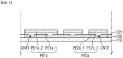
FIG. 8 is a cross-sectional view taken along line I-I' ofFIG. 7 ; -
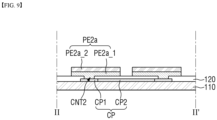
FIG. 9 is a cross-sectional view taken along line II-II' ofFIG. 7 ; -
FIG. 10 is an enlarged plan view of area A ofFIG. 4 according to another embodiment of the present disclosure; -
FIG. 11 is a plan view of a tiled display device according to an embodiment of the present disclosure; -
FIG. 12 is a perspective view illustrating a first pad area, a second pad area, a third pad area, a fourth pad area, and a fifth pad area of a first substrate according to another embodiment of the present disclosure; -
FIG. 13 is a detailed perspective view of a display device according to still another embodiment of the present disclosure; -
FIG. 14 is a perspective view illustrating a pad area and a side wiring area of a first substrate of a display device according to still another embodiment of the present disclosure; and -
FIG. 15 is a side view of the first substrate shown inFIG. 14 . - The advantages and features of the present invention, and methods of achieving them, will become clear upon reference to the embodiments described in detail below in conjunction with the accompanying drawings. However, the present invention is not limited to the embodiments disclosed below and may be implemented in other forms. In other words, the present invention is defined only by the scope of the claims.
- Elements or layers are referred to as "on" another element or layer, not just directly on top of the other element or layer, but also intervening with the other element or layer. Includes all cases. On the other hand, when an element is referred to as "directly on" or "directly on", it indicates that there is no intervening element or layer.
- The same reference numerals are used for identical or similar parts throughout the specification.
- Hereinafter, embodiments of the present disclosure will be described with reference to the attached drawings.
-
FIG. 1 is a perspective view of a display device according to an embodiment of the present disclosure.FIG. 2 is a detailed perspective view of the display device shown inFIG. 1 . - In
FIGS. 1 and2 , adisplay device 1 according to the embodiment of the present disclosure may be a subminiature light emitting diode display device (micro or nano light emitting diode display device) including a subminiature light emitting diode (micro or nano light emitting diode) as a light emitting element LE, but embodiments of the present disclosure are not limited thereto. - In addition, in
FIGS. 1 to 3 , a first direction DR1 refers to a horizontal direction of thedisplay device 1, a second direction DR2 refers to a vertical direction of thedisplay device 1, and a third direction DR3 refers to a thickness direction of thedisplay device 1. Also, the terms "left", "right", "upper", and "lower", as used herein, denote corresponding directions as viewed from above thedisplay device 1. For example, the term "right side" denotes one side in the first direction DR1, the term "left side" denotes the other side in the first direction DR1, the term "upper side" denotes one side in the second direction DR2, and the term "lower side" denotes the other side in the second direction DR2. Also, the term "upper portion" denotes one side in the third direction DR3, and the term "lower portion" denotes the other side in the third direction DR3. - Referring to
FIGS. 1 and2 , thedisplay device 1 may include afirst substrate 100, a printedcircuit film 400, and amain circuit board 500. - Although not illustrated in
FIGS. 1 and2 , thedisplay device 1 may further include various elements disposed on thefirst substrate 100. - For example, a micro light emitting diode (LED) may be used as the
display device 1. In the following embodiments, a micro LED may be used as thedisplay device 1. However, the present disclosure is not limited thereto, and different types of display device, such as an organic light emitting display (OLED), a liquid crystal display (LCD), a quantum dot organic light emitting display, a quantum dot liquid crystal display, a quantum nano light emitting display, and the like, may be used as the display device. - The various elements of the
first substrate 100 may include a plurality of insulating layers, a plurality of conductive layers, at least one thin film transistor, and a light emitting element electrically connected to the at least one thin film transistor. - For example, the
first substrate 100 may include a base substrate, a thin film transistor layer including the at least one thin film transistor, a wavelength conversion layer including at least one wavelength conversion pattern, and a color filter layer including at least one color filter. - The
first substrate 100 may include a base substrate. The base substrate of thefirst substrate 100 may include a rigid material, such as glass or quartz. - The
display device 1 may have a rectangular shape with right-angled corners in plan view. Thedisplay device 1 may have long sides and short sides in plan view. The short side of thedisplay device 1 may be a side extending in the first direction DR1. The long side of thedisplay device 1 may be a side extending in the second direction DR2. - The
first substrate 100 may include a display area DA. The display area DA of thefirst substrate 100 may include a plurality of pixels arranged thereon. Each of the pixels may include at least one thin film transistor and a light emitting element. - The display area DA may have a rectangular shape with right-angled or rounded corners in plan view. The display area DA may be substantially identical in shape with the
display device 1 in plan view. For example, the display area DA may have short sides and long sides. The long side of the display area DA may be a side extending in the second direction DR2. The short side of the display area DA may be a side extending in the first direction DR1. However, the planar shape of the display area DA is not limited to a rectangular shape, but may have a circular shape, an elliptical shape, or various other shapes. - The
display device 1 may further include a pad area PA. Thefirst substrate 100 of thedisplay device 1 may include the pad area PA. As shown inFIG. 2 , the pad area PA may be located on the other side of the display area DA in the second direction DR2. The pad area PA may be defined over a front surface (or one surface) of thefirst substrate 100, a back surface (or the other surface) opposite to the front surface, and a side surface between the front surface and the back surface. - The pad area PA may be attached to the printed
circuit film 400. One end of the printedcircuit film 400 may be attached to the pad area PA and the other end of the printedcircuit film 400 may be attached to themain circuit board 500. - As shown in
FIG. 2 , the printedcircuit film 400 may be attached to the back surface of thefirst substrate 100. -
FIG. 3 is a perspective view illustrating a first pad area, a second pad area, and a third pad area of the first substrate of the display device shown inFIG. 2 .FIG. 4 is a plan view of the first substrate shown inFIG. 3 .FIG. 5 is a side view of the first substrate shown inFIG. 3 .FIG. 6 is a rear view of the first substrate shown inFIG. 5 . - In
FIG. 3 , afront surface 100a, aside surface 100b, and aback surface 100c of thefirst substrate 100 are illustrated, and the other side portion in the second direction DR2 is enlarged to show the pad area PA of thefirst substrate 100 in more detail. - Referring to
FIGS. 3 to 6 , the pad area PA may include a first pad area PA1 located on thefront surface 100a of thefirst substrate 100, a second pad area PA2 located on theside surface 100b, and a third pad area PA3 located on theback surface 100c. - The
first substrate 100 may further include a first pad PE1, a second pad PE2, and a connection portion CP. The first pad PE1 may be a driving pad that electrically connects the printed circuit film 400 (seeFIG. 2 ) to the pixels of the display area DA, and the second pad PE2 may be a test pad for determining the disconnection of the first pad PE1. The connection portion CP may electrically connect the first pad PE1 to the second pad PE2. - As shown in
FIGS. 3 to 6 , the first pad PE1 may be disposed over the first to third pad areas PA1 to PA3. The second pad PE2 may be disposed in the first pad area PA1 and the third pad area PA3, but may not be disposed in the second pad area PA2. The connection portion CP may be disposed in the first pad area PA1 and the third pad area PA3, but may not be disposed in the second pad area PA2. - The first pad PE1, the second pad PE2, and the connection portion CP may each be provided in plural form. For example, the second pad PE2 and the connection portion CP may each be disposed between the adjacent first pads PE1, and one first pad PE1, one second pad PE2, and one connection portion CP may be grouped into a set.
- As shown in
FIGS. 3 and4 , the second pad PE2 may include separate patterns. For example, the second pad PE2 may include four separate patterns. The separate patterns of the second pad PE2 may be arranged in two columns in the first direction DR1 and two rows in the second direction DR2. For example, the separate patterns may be arranged in the form of a matrix arrangement. However, the disclosure is not limited thereto, and the separate patterns of the second pad PE2 may be five or more, or two to three, and may be randomly arranged, not in the form of a matrix arrangement. However, each of the separate patterns may be electrically connected (e.g., directly connected) to the connection portion CP and may be electrically connected to the first pad PE1 via the connection portion CP. For convenience of description, the following description will focus on the second pad PE2 including four separate patterns. - The first pad PE1 may include a first-first pad PE1a located in the first pad area PA1, a first-second pad PE1b located in the second pad area PA2, and a first-third pad PE1c located in the third pad area PA3. The first-first pad PE1a, the first-second pad PE1b, and the first-third pad PE1c may be electrically connected to one another. For example, the first-first pad PE1a and the first-second pad PE1b may be electrically connected (e.g., directly connected) to each other, and the first-second pad PE1b and the first-third pad PE1c may be electrically connected (e.g., directly connected) to each other. Further, the second pad PE2 may include a second-first pad PE2a located in the first pad area PA1 and a second-second pad PE2b located in the third pad area PA3.
- The first pad PE1, the second pad PE2, and the connection portion CP will be described in further detail with reference to
FIGS. 7 to 9 . -
FIG. 7 is an enlarged plan view of area A ofFIG. 6 .FIG. 8 is a cross-sectional view taken along line I-I' ofFIG. 7 .FIG. 9 is a cross-sectional view taken along line II-II' ofFIG. 7 . -
FIG. 7 shows the first-first pad PE1a of the first pad PE1, the connection portion CP, and the second-first pad PE2a. The stacked structure, the planar shape, or the like of the first-third pad PE1c, the connection portion CP, and the second-second pad PE2b that are located in the third pad area PA3 are substantially the same as those of the first-first pad PE1a, the connection portion CP, and the second-first pad PE2a, except the area where they are located is different from the area of the first-first pad PE1a, the connection portion CP, and the second-first pad PE2a. Therefore, descriptions of the first-third pad PE1c, the connection portion CP, and the second-second pad PE2b will be omitted. - Referring to
FIGS. 7 to 9 , the first-first pad PE1a may include a first lower pad portion PE1a_1 and a first upper pad portion PE1a_2 on the first lower pad portion PE1a_1, and the second-first pad PE2a may include a second lower pad portion PE2a_1 and a second upper pad portion PE2a_2 on the second lower pad portion PE2a_1. In addition, the connection portion CP may include a first connection portion CP1 extending along the first direction DR1 and a second connection portion CP2 extending along the second direction DR2. - The first lower pad portion PE1a_1 and the first upper pad portion PE1a_2 on the first lower pad portion PE1a_1 may overlap each other in a plan view. The second lower pad portion PE2a_1 and the second upper lower pad portion PE2a_2 on the second lower pad portion PE2a_1 may overlap each other in a plan view. The first lower pad portion PE1a_1 may have a rectangular shape in plan view. However, the planar shape of the first lower pad portion PE1a_1 is not limited to a rectangular shape, but may have a circular shape, an elliptical shape, or other polygonal shapes. The first upper pad portion PE1a_2 may have the same planar shape as that of the first lower pad portion PE1a_1, but is not limited thereto. The second lower pad portion PE2a_1 may have a rectangular shape in plan view. However, the planar shape of the second lower pad portion PE2a_1 is not limited to a rectangular shape, but may have a circular shape, an elliptical shape, or other polygonal shapes. The second upper pad portion PE2a_2 may have the same planar shape as that of the second lower pad portion PE2a_1, but is not limited thereto.
- As shown in
FIG. 7 , the area of the first-first pad PE1a may be greater than the area of the second-first pad PE2a in plan view. - The first connection portion CP1 may extend along the first direction DR1 as shown in
FIG. 7 , and may be provided in plural form. The first connection portion CP1 located on one side in the second direction DR2 in plan view and the first connection portion CP1 located on the other side in the second direction DR2 in plan view may be arranged in parallel to each other. Hereinafter, the first connection portion CP1 located on one side in the second direction DR2 will be referred to as an upper first connection portion CP1, and the first connection portion CP1 located on the other side in the second direction DR2 will be referred to as a lower first connection portion CP1. - The upper first connection portion CP1 may overlap one side portion of the first-first pad PE1a in the second direction DR2 and a row of the second-first pad PE2a on one side in the second direction DR2 in plan view, and the lower first connection portion CP1 may overlap the other side portion of the first-first pad PE1a in the second direction DR2 and a row of the second-first pad PE2a on the other side in the second direction DR2 in plan view.
- The second connection portion CP2 may extend along the first direction DR2 as shown in
FIG. 7 , and may be provided in plural form. The second connection portion CP2 located on one side in the first direction DR1 in plan view and the second connection portion CP2 located on the other side in the first direction DR1 in plan view may be arranged in parallel to each other. For example, adjacent ones of the second connection portions CP2 may be arranged in parallel to each other in the first direction DR1. Hereinafter, the second connection portion CP2 located on one side in the first direction DR1 will be referred to as a right second connection portion CP2, and the second connection portion CP2 located on the other side in the first direction DR1 will be referred to as a left second connection portion CP2. - The right second connection portion CP2 may overlap a row of the second-first pad PE2a on one side in the first direction DR1 in plan view, and the left second connection portion CP2 may overlap a row of the second-first pad PE2a on the other side in the first direction DR1 in plan view.
- The upper first connection portion CP1 may be electrically connected (e.g., directly connected) to an end of the left second connection portion CP2 in the second direction DR2 and an end of the right second connection portion CP2 in the second direction DR2. The lower first connection portion CP1 may be electrically connected (e.g., directly connected) to another end of the left second connection portion CP2 in the second direction DR2 and another end of the right second connection portion CP2 in the second direction DR2.
- Referring to
FIGS. 7 to 9 , thefirst substrate 100 may include afirst base member 110, a first conductive layer on thefirst base member 110, a first insulatinglayer 120 on the first conductive layer, a second conductive layer on the first insulatinglayer 120, and a third conductive layer on the second conductive layer. - The
first base member 110 may be made of a material having transparency. In some embodiments, thefirst base member 110 may be a glass substrate or a plastic substrate. In a case where thefirst base member 110 is a plastic substrate, thefirst base member 110 may have flexibility. - The first conductive layer may be disposed on the
first base member 110. In one embodiment, the first conductive layer may include the connection portion CP. Although not illustrated, the first conductive layer may further include a gate electrode of a thin film transistor, a first electrode of a reserve capacitor, a scan signal line that transmits a scan signal to the gate electrode. - The first conductive layer may include at least one metal selected from among molybdenum (Mo), aluminium (Al), platinum (Pt), palladium (Pd), silver (Ag), magnesium (Mg), gold (Au), nickel (Ni), neodymium (Nd), iridium (Ir), chromium (Cr), calcium (Ca), titanium (Ti), tantalum (Ta), tungsten (W), and copper (Cu). In addition, although the first conductive layer is a single film in the drawing, the first conductive layer may be a multilayer film. In this case, the multilayer film of the first conductive layer may be a stacked film made of different materials selected from the metals listed above.
- The first insulating
layer 120 may be disposed on the first conductive layer. The first insulatinglayer 120 may include an inorganic insulating material including at least one of silicon oxide, silicon nitride, silicon oxynitride, hafnium oxide, aluminium oxide, titanium oxide, tantalum oxide, and zirconium oxide, or an organic insulating material including at least one of a polyacrylate-based resin, an epoxy resin, a phenolic resin, a polyamide-based resin, a polyimide-based resin, an unsaturated polyester-based resin, a polyphenylene-ether-based resin, a polyphenylene sulfide-based resin, and benzocyclobutene (BCB). In the drawing, the first insulatinglayer 120 may be a single film, but is not limited thereto. The first insulatinglayer 120 may be a multilayer film consisting of a stacked film including different materials. - The second conductive layer may be disposed on the first insulating
layer 120. In one embodiment, the second conductive layer may include the first lower pad portion PE1a_1 and the second lower pad portion PE2a_1. In addition, although not illustrated, the second conductive layer may further include the source electrode, a drain electrode of the thin film transistor, and a supply voltage electrode of the thin film transistor. - The third conductive layer may be disposed on the second conductive layer. The third conductive layer may include the first upper pad portion PE1a_2 and the second upper pad portion PE2a_2. The third conductive layer may include a transparent conductive electrode. The transparent conductive electrode may include ITO or IZO. However, the third conductive layer may have the transparent conductive electrode or a metal layer containing at least one metal of Ag, Mg, Al, Pt, Pd, Au, Ni, Nd, Ir, and Cr. In an embodiment, the third conductive layer may have a multilayer structure, e.g., a double-layer structure of ITO/Ag, Ag/ITO, ITO/Mg and ITO/MgF, or a triple-layer structure of ITO/Ag/ITO, as well as the transparent conductive electrode.
- As shown in
FIGS. 8 and9 , the first lower pad portion PE1a_1 may be electrically connected to the first connection portion CP1 via a first contact hole CNT1. The second lower pad portion PE2a_1 may be electrically connected to the first connection portion CP1 via a second contact hole CNT2. InFIG. 9 , thefirst substrate 100 may include two first contact holes CNT1, but the disclosure is not limited thereto. Thefirst substrate 100 may include a first contact hole CNT1 or three or more first contact holes CNT1. Although inFIG. 9 thefirst substrate 100 may include the single second contact hole CNT2 connecting the first lower pad portion PE1a_1 to the first connection portion CP1, the disclosure is not limited thereto. Thefirst substrate 100 may include two or more second contact holes CNT2 that connect the first lower pad portion PE1a_1 to the first connection portion CP1. - The first upper pad portion PE1a_2 may be disposed on the first lower pad portion PE1a_1. The second upper pad portion PE2a_2 may be disposed on the second lower pad portion PE2a_1. The first upper pad portion PE1a_2 may be disposed (e.g., disposed directly) on the first lower pad portion PE1a_1. The second upper pad portion PE2a_2 may be disposed (e.g., disposed directly) on the second lower pad portion PE2a_1.
- The second-first pad PE2a according to an embodiment may include the separate patterns as described above. Further, the second-first pad PE2a may be a test pad for determining the disconnection of the first pad PE1. In the case that the test for the disconnection of the first pad PE1 is conducted using the second-first pad PE2a including only a pattern without the separate patterns, which is a test pad, delamination of the second-first pad PE2a may occur, and the probability of delamination of the first pad PE1 may be increased. In more detail, in the case that the test for determining the disconnection of the first pad PE1, which partially overlaps the second-first pad PE2a and the second-second pad PE2b in a plan view (e.g., in
FIG. 7 , the first-first pad PE1a overlaps the second-first pad PE2a and the first-third pad PE1c overlaps the second-second pad PE2b in the thickness direction), is performed by bringing a probe pin into contact with each of the second-first pad PE2a and the second-second pad PE2b, the contact with the probe pin may cause a physical impact to each of the second-first pad PE2a and the second-second pad PE2b, which may lead to the delamination of each of the second-first pad PE2a and the second-second pad PE2b. As a result, the first pad PE1 overlapping the second-first pad PE2a and the second-second pad PE2b in a plan view may be delaminated. - The first pad PE1 may be formed not to overlap each of the second-first pad PE2a and the second-second pad PE2b in a plan view. However, in the case that the probe pin is brought into contact with each of the second-first pad PE2a and the second-second pad PE2b, which is located very close to the first pad PE1, the probe pin may be in direct contact with the first pad PE1, and the direct contact may cause delamination of the first pad PE1.
- According to an embodiment, each of the second-first pad PE2a and the second-second pad PE2b may include separate patterns. Accordingly, even if the contact with the probe pin causes the physical impact to some separate patterns of the second-first pad PE2a and the second-second pad PE2b during the test for determining the disconnection of the first pad PE1 by bringing the probe pin into contact with each of the second-first pad PE2a and the second-second pad PE2b, the separate patterns of the second-first pad PE2a and the second-second pad PE2b may be less likely to be delaminated since the separate patterns are indirectly connected to other separate patterns of the second-first pad PE2a and the second-second pad PE2b via the connection portions CP.
- Even if some separate patterns of the second-first pad PE2a and the second-second pad PE2b are delaminated due to a physical impact caused by the contact with the probe pin, other separate patterns of the second-first pad PE2a and the second-second pad PE2b may be physically spaced apart from the separate patterns and thus delamination of other separate patterns of the second-first pad PE2a and the second-second pad PE2b may be prevented. Thus, the probability of delamination of the first pad PE1 may be significantly reduced.
- Hereinafter, other embodiments are described below.
-
FIG. 10 is an enlarged plan view of area A ofFIG. 4 according to another embodiment of the present disclosure. - Referring to
FIG. 10 , the embodiment is different from the display device ofFIG. 8 at least in that a second lower pad portion PE2a'_1 has a rectangular shape having long sides extending in the second direction DR2 and short sides extending in the first direction DR1 in a plan view and a second-first pad PE2a' includes two separate patterns. - However, the second lower pad portion PE2a'_1 is not limited to the rectangular shape, but may have a circular shape, an elliptical shape, or other polygonal shapes. A second upper pad portion PE2a'_2 and the second lower pad portion PE2a'_1 may have a same planar shape, but is not limited thereto.
- According to the embodiment, the second-first pad PE2a' includes a plurality of separate patterns. Accordingly, even if the contact with a probe pin causes a physical impact to some separate patterns of the second-first pad PE2a' during a test for determining the disconnection of a first pad PE1 by bringing the probe pin into contact with the second-first pad PE2a', the separate patterns of the second-first pad PE2a' may be less likely to be delaminated since the separate patterns are indirectly connected to the other separate patterns of the second-first pad PE2a' via a connection portion CP.
- Even if some separate patterns of the second-first pad PE2a' are delaminated due to the physical impact caused by the contact with the probe pin, other separate patterns of the second-first pad PE2a' may be physically spaced apart from the separate patterns. Thus, delamination of other separate patterns of the second-first pad PE2a' may be prevented. Therefore, the probability of delamination of the first pad PE1 may be significantly reduced.
-
FIG. 11 is a plan view of a tiled display device according to an embodiment of the present disclosure. - Referring to
FIG. 11 , a display device according to the embodiment differs from thedisplay device 1 ofFIG. 1 at least in thatmultiple display devices 1 are used as a tiled display device TD. - For example, in an embodiment, the
display devices 1 may be arranged in a grid shape, but the disclosure is not limited thereto. For example, thedisplay devices 1 may be arranged to be connected in a direction, connected in another direction that intersects the direction, and connected to have a shape. Thedisplay devices 1 may have a same size, but the disclosure is not limited thereto, and thedisplay devices 1 may be of different sizes. - Each of the
display devices 1 is described above with reference toFIGS. 1 to 3 , and thus redundant descriptions thereof will be omitted. - The
display devices 1 may be disposed such that the long sides or short sides are connected to each other. Some of thedisplay devices 1 may form a side of the tiled display device TD, and some of thedisplay devices 1 may be located at a corner of the tiled display device TD to form two adjacent sides of the tiled display device TD, and some of thedisplay devices 1 may form a structure in which somedisplay devices 1 are located inside the tiled display device TD to be surrounded byother display devices 1. Thedisplay devices 1 may have different bezel shapes according to their positions and may have the same bezel shape. - The
display devices 1 of the tiled display device TD may be aflat display device 1, but the present disclosure is not limited thereto. The tiled display device TD may have a three-dimensional shape so as to provide a three-dimensional effect. In a case where the tiled display device TD has a three-dimensional shape, each of thedisplay devices 1 included in the tiled display device TD may have a curved shape and may be connected to each other in a flat shape or at a predetermined angle to three-dimensionally form an entire shape of the tiled display device TD. -
FIG. 12 is a perspective view illustrating a first pad area, a second pad area, a third pad area, a fourth pad area, and a fifth pad area of a first substrate according to another embodiment of the present disclosure. - Referring to
FIG. 12 , a first substrate 100_1 according to the current embodiment differs from thefirst substrate 100 ofFIG. 3 in that the first substrate 100_1 further includes afirst surface 100d between afront surface 100a and aside surface 100b and asecond surface 100e between theside surface 100b and aback surface 100c and a pad area PA_1 further includes a fourth pad area PA4 on thefirst surface 100d and a fifth pad area PA5 on thesecond surface 100e. - The first substrate 100_1 of the current embodiment is different from the
first substrate 100 ofFIG. 3 in that a first pad PE1 is disposed over the first to fifth pad areas PA1 to PA5. - Other descriptions have been described above, and redundant descriptions will be omitted.
-
FIG. 13 is a detailed perspective view of a display device according to still another embodiment of the present disclosure. - Referring to
FIG. 13 , adisplay device 2 according to the embodiment differs from thedisplay device 1 ofFIGS. 1 and2 at least in that thedisplay device 2 may further include asecond substrate 300 opposite to thefirst substrate 100. - The
first substrate 100 and thesecond substrate 300 may have substantially the same shape in plan view. One side portion (lower short side portions in the second direction DR2) of thefirst substrate 100 and thesecond substrate 300 are polished so that one side surface of thefirst substrate 100 and one side surface of thesecond substrate 300 may be aligned along a thickness direction (third direction DR3). In the other side portions (upper short side portions in the second direction DR2, right long side portion in the first direction DR1, and left long side portions in the first direction DR1) of thefirst substrate 100 and thesecond substrate 300, the side surfaces of thefirst substrate 100 and thesecond substrate 300 may be aligned along the thickness direction, but the present disclosure is not limited thereto. - Each of the
first substrate 100 and thesecond substrate 300 may include a base substrate. The base substrates of thefirst substrate 100 and thesecond substrate 300 may each include a rigid material, such as glass or quartz. - In the current embodiment, the
first substrate 100 may be a thin film transistor substrate on which a thin film transistor layer including at least one thin film transistor is disposed. A wavelength conversion layer including at least one wavelength conversion pattern and a color filter layer including at least one color filter may be disposed on thesecond substrate 300. - A non-display area NDA of the
first substrate 100 may be disposed around a display area DA. The non-display area NDA may be disposed adjacent to both short sides and both long sides of the display area DA. In this case, the non-display area NDA may surround all sides of the display area DA to form an edge of the display area DA. However, the present disclosure is not limited thereto, and the non-display area NDA may be disposed adjacent to only both short sides or both long sides of the display area DA. - Although not illustrated, the non-display area NDA of the
first substrate 100 according to the current embodiment may further include a sealing area. The sealing area may be disposed in the non-display area NDA to run along the edges of the first andsecond substrates second substrates second substrates - The sealing area may have a shape of a rectangle frame arranged to run along the edges of the first and
second substrates - Other descriptions have been described above with reference to
FIGS. 2 and3 , and redundant descriptions will be omitted. -
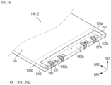
FIG. 14 is a perspective view illustrating a pad area and a side wiring area of a first substrate of a display device according to still another embodiment of the present disclosure.FIG. 15 is a side view of the first substrate shown inFIG. 14 . - Referring to
FIGS. 14 and15 , a first substrate 100_2 of a display device according to the current embodiment differs from thefirst substrate 100 ofFIG. 3 in that the first substrate 100_2 does not include a second pad area PA2 and a side wiring area SPA is disposed in an area that corresponds to the second pad area PA2. - For example, the side wiring area SPA may be disposed between a first pad area PA1 and a third pad area PA3 and connect the first pad area PA1 to the third pad area PA3.
- As shown in
FIGS. 3 to 6 , the first pad PE1 is disposed in the first pad area PA1 and the third pad area PA3, and may not be disposed in the side wiring area SPA. A second pad PE2 may be disposed in the first pad area PA1 and the third pad area PA3, and may not be disposed in the side wiring area SPA. A connection portion CP may be disposed in the first pad area PA1 and the third pad area PA3, and may not be disposed in the side wiring area SPA. - The first pad PE1 may include a first-first pad PE1a located in the first pad area PA1 and a first-third pad PE1c located in the third pad area PA3. A side wiring SPE may be disposed between the first-first pad PE1a and the first-third pad PE1c. An end of the side wiring SPE may be electrically connected to the first-first pad PE1a and another end of the side wiring SPE may be electrically connected to the first-third pad PE1c. For example, the first-first pad PE1a and the side wiring SPE may be electrically connected (e.g., directly connected) to each other, and the side wiring SPE and the first-third pad PE1c may be electrically connected (e.g., directly connected) to each other. Further, the second pad PE2 may include a second-first pad PE2a located in the first pad area PA1 and a second-second pad PE2b located in the third pad area PA3.
- Although some example embodiments of the present disclosure have been described above, these are merely examples and do not limit the present disclosure. Further, the present disclosure may be changed and modified in various ways, without departing from the features of the present disclosure, by those skilled in the art. For example, the components described in the example embodiments of the present disclosure may be modified. Differences related to these modifications and applications should be construed as being within the scope of the present disclosure defined by the claims.
Claims (20)
- A display device comprising:a substrate comprising:a display area comprising pixels;a pad area comprising a plurality of pads and located adjacent to the display area; anda side wiring area located adjacent to the display area; anda printed circuit film attached to the pad area located on a back surface of the substrate, whereinthe plurality of pads comprise:a plurality of first pads that electrically connect the printed circuit film to the pixels; anda second pad disposed between the adjacent first pads,the display device further comprises a connection portion that electrically connects the first pad and the second pad to each other,the first pad comprises a first-first pad located on a front surface of the substrate; anda first-second pad located on the back surface of the substrate, andthe display device further comprises side wirings that are disposed in the side wiring area and electrically connect the first-first pad and the first-second pad to each other.
- The display device of claim 1, wherein the pad area comprises a first pad area located on the front surface of the first substrate and a second pad area located on the back surface of the substrate and
wherein the side wiring area is disposed on a side surface between the front surface of the substrate and the back surface of the substrate. - The display device of claim 2, wherein the first-first pad is disposed in the first pad area, and
wherein the first-second pad is disposed in the second pad area. - The display device of claim 3, wherein the printed circuit film is attached onto the second pad area through an anisotropic conductive film.
- The display device of claim 3, wherein the second pad is disposed in the first pad area and the second pad area, and
wherein the second pad is not disposed in the side wiring area. - The display device of claim 5, wherein the connection portion is disposed in the first pad area and the second pad area, and
wherein the connection portion is not disposed in the side wiring area. - The display device of claim 6, wherein each of the second pad and the connection portion is provided in a plural.
- The display device of claim 7, wherein the second pad and the connection portion are respectively connected to an adjacent first pad of the plurality of first pads in a plan view.
- The display device of claim 6, wherein the second pad comprises a plurality of patterns separated from each other.
- The display device of claim 9, wherein the plurality of patterns of the second pad are electrically connected to the first pad via the connection portion.
- The display device of claim 10, wherein the first pad comprises a first lower pad portion and a first upper pad portion on the first lower pad portion, and
wherein the first lower pad portion is directly connected to the connection portion. - The display device of claim 11, wherein the plurality of patterns of the second pad comprises a second lower pad portion and a second upper pad portion on the second lower pad portion and
wherein the second lower pad portion is connected directly to the connection portion. - The display device of claim 12, wherein the first lower pad portion is disposed on the same layer as the second lower pad portion.
- The display device of claim 13, wherein the first upper pad portion is disposed on the same layer as the second upper pad portion.
- A display device comprising:a first substrate comprising a display area comprising pixels, a pad area comprising a plurality of pads and located adjacent to the display area and a side wiring area located adjacent to the display area;a second substrate opposite to the first substrate; anda printed circuit film attached to the pad area located on a back surface of the first substrate,wherein:a plurality of pads of the first substrate are disposed in the pad area,the plurality of pads comprise a plurality of first pads that electrically connect the printed circuit film to the pixels, and a second pad disposed between the adjacent first pads and comprising a plurality of patterns,the display device further comprises a connection portion configured to connect the first pad and the plurality of patterns of the second pad to each other,the first pad comprises a first-first pad located on a front surface of the first substrate and a first-second pad located on the back surface of the first substrate, andthe display device further comprises side wirings that are disposed in the side wiring area and electrically connect the first-first pad and the first-second pad to each other.
- The display device of claim 15, wherein the pad area comprises a first pad area located on the front surface of the first substrate and a second pad area located on the back surface of the first substrate, and
wherein the first pad is disposed in the first pad area and the second pad area. - The display device of claim 16, wherein the second pad is disposed in the first pad area and the second pad area, and
wherein the connection portion is disposed in the first pad area and the second pad area. - The display device of claim 17, wherein each of the second pad and the connection portion is provided in a plural, and
wherein the second pads and the connection portions are respectively connected to the first pads adjacent thereto. - A tiled display device comprising:first substrates each comprising a display area comprising pixels, a pad area comprising a plurality of pads and located adjacent to the display area, and a side wiring area comprising side wirings and located adjacent to the display area; anda printed circuit film attached to the pad area located on a back surface of the first substrate,wherein the first substrate comprises:a base substrate,a first conductive layer comprising a connection portion on the base substrate,an insulating layer on the first conductive layer,a second conductive layer comprising a first lower pad portion on the conductive layer and a second lower pad portion, anda third conductive layer comprising a first upper pad portion overlapping the first lower pad portion on the second conductive layer in a plan view and a second upper pad portion overlapping the second lower pad portion in a plan view,wherein:the pads comprise a plurality of first pads that electrically connect the printed circuit film to the pixels, and a second pad disposed between the adjacent first pads,the first pad comprises a first-first pad located on a front surface of the first substrate and a first-second pad located on the back surface of the first substrate,the side wirings electrically connect the first-first pad and the first-second pad to each other,the first lower pad portion and the first upper pad portion form the first-first pad, andthe second lower pad portion and the second upper pad portion form the second pad.
- The tiled display device of claim 19, wherein the pad area comprises a first pad area located on the front surface of the first substrate and a second pad area located on the back surface of the first substrate, and
wherein the side wiring area connects the first pad area and the second pad area to each other.
Applications Claiming Priority (2)
| Application Number | Priority Date | Filing Date | Title |
|---|---|---|---|
| KR1020220011527A KR20230115381A (en) | 2022-01-26 | 2022-01-26 | Display device and tile-type display device including same |
| PCT/KR2023/000860 WO2023146204A1 (en) | 2022-01-26 | 2023-01-18 | Display device and tiled display device comprising same |
Publications (2)
| Publication Number | Publication Date |
|---|---|
| EP4471858A1 true EP4471858A1 (en) | 2024-12-04 |
| EP4471858A4 EP4471858A4 (en) | 2025-11-19 |
Family
ID=87314667
Family Applications (1)
| Application Number | Title | Priority Date | Filing Date |
|---|---|---|---|
| EP23747246.9A Pending EP4471858A4 (en) | 2022-01-26 | 2023-01-18 | Display device and mosaic display device with which |
Country Status (7)
| Country | Link |
|---|---|
| US (2) | US12520642B2 (en) |
| EP (1) | EP4471858A4 (en) |
| JP (1) | JP2025503860A (en) |
| KR (1) | KR20230115381A (en) |
| CN (1) | CN116504767A (en) |
| TW (1) | TW202338767A (en) |
| WO (1) | WO2023146204A1 (en) |
Families Citing this family (1)
| Publication number | Priority date | Publication date | Assignee | Title |
|---|---|---|---|---|
| CN114975746B (en) * | 2022-05-20 | 2025-07-22 | Tcl华星光电技术有限公司 | Display panel, printing device and preparation method of display panel |
Family Cites Families (19)
| Publication number | Priority date | Publication date | Assignee | Title |
|---|---|---|---|---|
| KR101337167B1 (en) | 2008-12-24 | 2013-12-05 | 엘지디스플레이 주식회사 | Method of fabricating display device |
| US10896931B1 (en) | 2010-10-11 | 2021-01-19 | Monolithic 3D Inc. | 3D semiconductor device and structure |
| KR101301424B1 (en) | 2011-11-28 | 2013-08-28 | 삼성전기주식회사 | Printed circuit board and method of manufacturing the same |
| US10875145B2 (en) | 2014-10-17 | 2020-12-29 | Applied Materials, Inc. | Polishing pads produced by an additive manufacturing process |
| KR102518426B1 (en) | 2016-09-09 | 2023-04-05 | 삼성디스플레이 주식회사 | Display device |
| KR102613852B1 (en) | 2016-12-29 | 2023-12-15 | 엘지디스플레이 주식회사 | Flexible Display Device |
| KR102433358B1 (en) | 2017-12-05 | 2022-08-16 | 엘지디스플레이 주식회사 | Display device |
| KR102457907B1 (en) | 2017-12-29 | 2022-10-25 | 삼성디스플레이 주식회사 | Display device |
| KR102581839B1 (en) | 2018-10-02 | 2023-09-22 | 삼성디스플레이 주식회사 | Display device |
| KR102936695B1 (en) | 2018-12-19 | 2026-03-10 | 삼성전자주식회사 | Display module and manufacturing method of display module |
| CN110164901B (en) * | 2019-06-25 | 2021-10-22 | 京东方科技集团股份有限公司 | Array substrate and preparation method thereof, display panel and display device |
| CN112748816B (en) * | 2019-10-30 | 2022-10-21 | 群创光电股份有限公司 | display panel |
| KR102696659B1 (en) * | 2019-11-22 | 2024-08-19 | 엘지디스플레이 주식회사 | Light emitting display apparatus |
| CN113644181B (en) * | 2020-05-11 | 2024-04-16 | 京东方科技集团股份有限公司 | Light-emitting substrate and method for manufacturing the same, and display device |
| KR20220096922A (en) * | 2020-12-31 | 2022-07-07 | 엘지디스플레이 주식회사 | Light emitting display apparatus and multi screen display apparatus using the same |
| KR20220096921A (en) * | 2020-12-31 | 2022-07-07 | 엘지디스플레이 주식회사 | Light emitting display apparatus and multi screen display apparatus using the same |
| KR20220096887A (en) * | 2020-12-31 | 2022-07-07 | 엘지디스플레이 주식회사 | Display apparatus and multi screen display apparatus using the same |
| KR102945598B1 (en) * | 2020-12-31 | 2026-03-27 | 엘지디스플레이 주식회사 | Light emitting display apparatus and multi screen display apparatus using the same |
| CN117063221B (en) * | 2021-05-25 | 2026-02-24 | 京东方科技集团股份有限公司 | Display panel, manufacturing method thereof, display device and spliced display device |
-
2022
- 2022-01-26 KR KR1020220011527A patent/KR20230115381A/en active Pending
-
2023
- 2023-01-03 US US18/092,523 patent/US12520642B2/en active Active
- 2023-01-18 JP JP2024539078A patent/JP2025503860A/en active Pending
- 2023-01-18 TW TW112102315A patent/TW202338767A/en unknown
- 2023-01-18 CN CN202310073953.XA patent/CN116504767A/en active Pending
- 2023-01-18 EP EP23747246.9A patent/EP4471858A4/en active Pending
- 2023-01-18 WO PCT/KR2023/000860 patent/WO2023146204A1/en not_active Ceased
-
2025
- 2025-12-17 US US19/423,719 patent/US20260114095A1/en active Pending
Also Published As
| Publication number | Publication date |
|---|---|
| TW202338767A (en) | 2023-10-01 |
| US12520642B2 (en) | 2026-01-06 |
| CN116504767A (en) | 2023-07-28 |
| WO2023146204A1 (en) | 2023-08-03 |
| EP4471858A4 (en) | 2025-11-19 |
| US20230238498A1 (en) | 2023-07-27 |
| US20260114095A1 (en) | 2026-04-23 |
| JP2025503860A (en) | 2025-02-06 |
| KR20230115381A (en) | 2023-08-03 |
Similar Documents
| Publication | Publication Date | Title |
|---|---|---|
| CN110096170B (en) | Display Devices | |
| KR102903691B1 (en) | Display device | |
| US20260114095A1 (en) | Display device and tiled display device including the same | |
| US20250081696A1 (en) | Display device | |
| CN112449486B (en) | Display Devices | |
| KR20240040157A (en) | Display device | |
| US11409335B2 (en) | Display device | |
| KR20220142597A (en) | Display device and method of manufacturing the same | |
| US11540392B2 (en) | Display device and film package | |
| CN114388573A (en) | Display device and apparatus for manufacturing the same | |
| CN112563304A (en) | Display device | |
| CN112820754A (en) | display screen | |
| US20260087972A1 (en) | Display device | |
| US11917875B2 (en) | Display device | |
| CN112289261B (en) | Display Devices | |
| US20260052859A1 (en) | Display module and electronic device including the same | |
| US20220328439A1 (en) | Display device | |
| KR20250098054A (en) | Display device and method of manufacturing the same | |
| CN121419431A (en) | Display devices and display panels | |
| KR20220155512A (en) | Display device | |
| KR20140143605A (en) | Organic Light-Emitting Diode Display Device |
Legal Events
| Date | Code | Title | Description |
|---|---|---|---|
| STAA | Information on the status of an ep patent application or granted ep patent |
Free format text: STATUS: THE INTERNATIONAL PUBLICATION HAS BEEN MADE |
|
| PUAI | Public reference made under article 153(3) epc to a published international application that has entered the european phase |
Free format text: ORIGINAL CODE: 0009012 |
|
| STAA | Information on the status of an ep patent application or granted ep patent |
Free format text: STATUS: REQUEST FOR EXAMINATION WAS MADE |
|
| 17P | Request for examination filed |
Effective date: 20240719 |
|
| AK | Designated contracting states |
Kind code of ref document: A1 Designated state(s): AL AT BE BG CH CY CZ DE DK EE ES FI FR GB GR HR HU IE IS IT LI LT LU LV MC ME MK MT NL NO PL PT RO RS SE SI SK SM TR |
|
| DAV | Request for validation of the european patent (deleted) | ||
| DAX | Request for extension of the european patent (deleted) | ||
| REG | Reference to a national code |
Ref country code: DE Ref legal event code: R079 Free format text: PREVIOUS MAIN CLASS: H01L0025075000 Ipc: G09F0009302000 |
|
| A4 | Supplementary search report drawn up and despatched |
Effective date: 20251020 |
|
| RIC1 | Information provided on ipc code assigned before grant |
Ipc: G09F 9/302 20060101AFI20251014BHEP Ipc: G09F 9/33 20060101ALI20251014BHEP Ipc: H05K 3/36 20060101ALI20251014BHEP Ipc: H01L 25/16 20230101ALN20251014BHEP Ipc: H05K 1/11 20060101ALN20251014BHEP Ipc: H10K 59/10 20230101ALN20251014BHEP |
|
| P01 | Opt-out of the competence of the unified patent court (upc) registered |
Free format text: CASE NUMBER: UPC_APP_0007258_4471858/2026 Effective date: 20260226 |