EP4468519A1 - Electronic beam-steering reflectarray antenna system with varactor diode embedded comb-shaped unit cell - Google Patents
Electronic beam-steering reflectarray antenna system with varactor diode embedded comb-shaped unit cell Download PDFInfo
- Publication number
- EP4468519A1 EP4468519A1 EP24172467.3A EP24172467A EP4468519A1 EP 4468519 A1 EP4468519 A1 EP 4468519A1 EP 24172467 A EP24172467 A EP 24172467A EP 4468519 A1 EP4468519 A1 EP 4468519A1
- Authority
- EP
- European Patent Office
- Prior art keywords
- comb
- unit cell
- reflection phase
- length
- trunk
- Prior art date
- Legal status (The legal status is an assumption and is not a legal conclusion. Google has not performed a legal analysis and makes no representation as to the accuracy of the status listed.)
- Granted
Links
Images













Classifications
-
- H—ELECTRICITY
- H01—ELECTRIC ELEMENTS
- H01Q—ANTENNAS, i.e. RADIO AERIALS
- H01Q3/00—Arrangements for changing or varying the orientation or the shape of the directional pattern of the waves radiated from an antenna or antenna system
- H01Q3/44—Arrangements for changing or varying the orientation or the shape of the directional pattern of the waves radiated from an antenna or antenna system varying the electric or magnetic characteristics of reflecting, refracting, or diffracting devices associated with the radiating element
- H01Q3/46—Active lenses or reflecting arrays
-
- H—ELECTRICITY
- H01—ELECTRIC ELEMENTS
- H01Q—ANTENNAS, i.e. RADIO AERIALS
- H01Q15/00—Devices for reflection, refraction, diffraction or polarisation of waves radiated from an antenna, e.g. quasi-optical devices
- H01Q15/0006—Devices acting selectively as reflecting surface, as diffracting or as refracting device, e.g. frequency filtering or angular spatial filtering devices
- H01Q15/006—Selective devices having photonic band gap materials or materials of which the material properties are frequency dependent, e.g. perforated substrates, high-impedance surfaces
- H01Q15/0066—Selective devices having photonic band gap materials or materials of which the material properties are frequency dependent, e.g. perforated substrates, high-impedance surfaces said selective devices being reconfigurable, tunable or controllable, e.g. using switches
-
- H—ELECTRICITY
- H01—ELECTRIC ELEMENTS
- H01Q—ANTENNAS, i.e. RADIO AERIALS
- H01Q15/00—Devices for reflection, refraction, diffraction or polarisation of waves radiated from an antenna, e.g. quasi-optical devices
- H01Q15/14—Reflecting surfaces; Equivalent structures
- H01Q15/148—Reflecting surfaces; Equivalent structures with means for varying the reflecting properties
-
- H—ELECTRICITY
- H01—ELECTRIC ELEMENTS
- H01Q—ANTENNAS, i.e. RADIO AERIALS
- H01Q19/00—Combinations of primary active antenna elements and units with secondary devices, e.g. with quasi-optical devices, for giving the antenna a desired directional characteristic
- H01Q19/10—Combinations of primary active antenna elements and units with secondary devices, e.g. with quasi-optical devices, for giving the antenna a desired directional characteristic using reflecting surfaces
- H01Q19/108—Combination of a dipole with a plane reflecting surface
-
- H—ELECTRICITY
- H01—ELECTRIC ELEMENTS
- H01Q—ANTENNAS, i.e. RADIO AERIALS
- H01Q9/00—Electrically-short antennas having dimensions not more than twice the operating wavelength and consisting of conductive active radiating elements
- H01Q9/04—Resonant antennas
- H01Q9/16—Resonant antennas with feed intermediate between the extremities of the antenna, e.g. centre-fed dipole
Definitions
- the disclosure herein generally relates to the field of antenna based reflect array system, and, more particularly, to electronic beam-steering reflectarray antenna system with varactor diode embedded comb-shaped unit cell.
- phased antenna arrays consist of multiple antenna elements, wherein each antenna element is fed with different phase shifts to tilt the resultant beam in a desired direction.
- the main challenge in this type of architecture is that there must be a separate phase shifters network with many phase shifters. Further the phase shifters increase cost and complexity of the system.
- Metasurfaces are two-dimensional (2D) version of metamaterials with negligible thickness comprising several unit cells of sub-wavelength dimensions, arranged periodically over a substrate surface.
- the varactor diodes are placed in each of the unit cells in such a way to provide it with the direct current (DC) biasing network.
- DC direct current
- the metasurface can transmit, reflect, or absorb an electromagnetic beam.
- a tunable metasurface-based flat panel reflector with the integrated varactor diode or the PIN diode has been studied in recent times and different new designs of the same are explored.
- new designs which relate to a novel unit cell structures have continuously been explored for the purpose of higher frequency of operation, higher radiation efficiency, and higher frequency bandwidth, higher directivity, high efficiency, low profile, and ease of setting beam tilt angle with precision.
- a precise technique of synthesizing and evaluating new unit cells is needed.
- the reflection phase gradient required for a desired beam tilt angle is computed using generalized Snell's law. Theoretically it is possible to obtain the required inter-element refection phase gradient by changing capacitance values embedded in each unit cell. But the implementation becomes significantly challenging since the reflection phase gradient rapidly changes with small changes in the capacitance values. Moreover, for wide beam tilt angle the reflection phase gradient need to cover entire range of 0 degree to 360 degree. However, there isn't any standard way to achieve the wide beam tilt angle to cover entire range of 0 degree to 360 degree for better designing the metasurface based beam-steering antennas.
- Embodiments of the present disclosure present technological improvements as solutions to one or more of the above-mentioned technical problems recognized by the inventors in conventional systems.
- an electronic beam-steering reflectarray antenna system with varactor diode embedded comb-shaped unit cell comprising: a reflectarray metasurface positioned at a predetermined height below a standard half-wavelength dipole antenna; a plurality of comb-shaped unit cells arranged as a matrix over the reflectarray metasurface, wherein each of the plurality of comb-shaped unit cells is designed as one of (i) a first unit cell structure and (ii) a second unit cell structure, and wherein the first unit cell structure comprising: a comb shaped structure with a comb shaped first part and a comb shaped second part separated by a predefined gap to mount a varactor diode at a designated position, wherein the comb shaped first part comprising a first trunk, and a plurality of first arms comprising a first top arm, a first center arm and a first bottom arm, wherein the comb shaped second part comprising a second trunk, and a plurality of second arms comprising
- the design of the second unit cell structure comprising: a variation to the first unit cell structure with an additional copper layer positioned below the copper bottom layer reflector through a hole with the second cylindrical metal post from the first center arm, a second dielectric substrate separating the copper bottom layer reflector and the additional copper layer, and wherein length of the first trunk is less than length of the comb-shaped unit cell structure in the X-direction.
- the electronic beam-steering reflectarray antenna system is controlled by a control unit comprising one or more hardware processors, coupled to a memory via one or more communication interfaces.
- the one or more hardware processors are configured by the instructions to tilt the reflected beam in a desired direction, from the obtained plurality of reflection phase responses by: identifying, a reflection phase gradient of the reflectarray meta surface, from a plurality reflection phase responses corresponding to each of the plurality of unit cells for a desired angle received from a user; obtaining, a capacitance value of a plurality of capacitance values, for each of the plurality of unit cells, from the reflection phase gradient; mapping, the obtained plurality of capacitance values to the DC voltages corresponding to the varactor diodes using a predefined lookup table; and applying, suitable DC voltage to the varactor diode in each of the plurality of unit cells, to tilt the reflected beam over a desired direction.
- a method for optimizing design of a first unit cell structure and a second unit structure includes optimizing, via an optimization technique executed by one or more hardware processors of a control unit controlling an electronic beam-steering reflectarray antenna system, a design of one of (i) a first unit cell structure and (ii) a second unit cell structure of a comb shaped unit cell of the electronic beam-steering reflectarray antenna system.
- the optimization technique for optimizing the design of the first unit cell structure comprising: performing simulation comprising a mode1 simulation and a mode2 simulation on the first unit cell structure to (i) obtain an optimum comb arm length corresponding to the plurality of first arms, the second top arm, and the second bottom arm and (ii) estimate a plurality of reflection phase responses by: (a) setting a plurality of parameters of the first unit cell structure as constant values except comb arm length corresponding to the plurality of first arms, the second top arm, and the second bottom arm; (b) obtaining a plurality of frequency variations of an incident electromagnetic wave and a corresponding plurality of reflection phase responses of a reflected beam, without mounting the varactor diode on the first unit cell structure, for a plurality of comb arm length variations, wherein the comb arm length varies between first value and a second value by steps of a predefined value, wherein varying the comb arm length enables the plurality of frequency variations between a first frequency value and
- the optimization technique for optimizing the design of the second unit cell structure comprising: performing simulation comprising mode1 simulation and a mode2 simulation on the second unit cell structure, (i) to obtain the optimum comb arm length corresponding to the plurality of first arms, the second top arm, and the second bottom arm and an optimum comb trunk length corresponding to the first trunk, and (ii) to estimate the plurality of reflection phase responses by: (a) setting the plurality of parameters of the second unit cell structure as constant values except the comb arm length corresponding to the plurality of first arms, the second top arm, and the second bottom arm, and length of the first trunk; (b) obtaining the plurality of frequency variations of an incident electromagnetic wave and the corresponding plurality of reflection phase responses of the reflected beam, without mounting the varactor diode on the second unit cell structure, for the plurality of comb arm length variations, wherein the comb arm length varies between first value and a second value by steps of a predefined value, wherein initially the length of the first
- the one or more hardware processors are configured by the instructions to tilt the reflected beam in a desired direction, from the obtained plurality of reflection phase responses by: identifying, a reflection phase gradient of the reflectarray meta surface, from a plurality reflection phase responses corresponding to each of the plurality of unit cells for a desired angle received from a user; obtaining, a capacitance value of a plurality of capacitance values, for each of the plurality of unit cells, from the reflection phase gradient; mapping, the obtained plurality of capacitance values to the DC voltages corresponding to the varactor diodes using a predefined lookup table; and applying, suitable DC voltage to the varactor diode in each of the plurality of unit cells, to tilt the reflected beam over the desired direction.
- one or more non-transitory machine-readable information storage mediums comprising one or more instructions which when executed by one or more hardware processors cause a method for optimizing design of a first unit cell structure and a second unit structure.
- the method includes optimizing, via an optimization technique executed by one or more hardware processors of a control unit controlling an electronic beam-steering reflectarray antenna system, a design of one of (i) a first unit cell structure and (ii) a second unit cell structure of a comb shaped unit cell of the electronic beam-steering reflectarray antenna system.
- the present disclosure optimizes design of the plurality of comb-shaped unit cells arranged over a reflectarray metasurface.
- the plurality of comb-shaped unit cells is designed as one of (i) a first unit cell structure and (ii) a second unit cell structure.
- a standard half-wavelength dipole antenna is integrated with the proposed reflectarray metasurface to produce electronically steerable antenna.
- the reflectarray metasurface is positioned at a predetermined height below the standard half-wavelength dipole antenna.
- Each of the plurality of comb-shaped unit cell is embedded with a commercially available varactor diode. These varactor diodes, when driven by appropriate direct current (DC) biasing voltages offer different capacitance values.
- DC direct current
- each of the plurality of comb-shaped units cell gets different DC bias voltages, then the reflectarray metasurface gets transformed to a programmable structure whose reflection phase gradient can be adjusted which in turn helps in tilting a reflected beam over a desired direction.
- the DC bias voltage adjustment is controlled digitally where the user feeds the desired angle which leads to computing the necessary reflection phase gradient (Generalized Snell's law) followed by selecting necessary capacitance values and the corresponding DC bias voltages for each of the plurality of comb-shaped unit cells.
- the plurality of comb-shaped unit cells designed as the first unit cell structure helps in tilting the reflected beam over the desired direction in a single line.
- the plurality of comb-shaped unit cells designed as the second unit cell structure helps in tilting the reflected beam over the desired direction in a two-dimensional (2D) plane.
- ⁇ r reflection angle
- ⁇ i incidence angle
- n i reffractive index of the medium in which reflection is taking place
- n i wavelength of operation.
- FIG. 1 through FIG. 17B where similar reference characters denote corresponding features consistently throughout the figures, there are shown preferred embodiments and these embodiments are described in the context of the following exemplary system and/or method.
- FIG. 1 illustrates an exemplary block diagram of an electronic beam-steering reflectarray antenna system 100, in accordance with some embodiments of the present disclosure.
- the embodiment the electronic beam-steering reflectarray antenna system 100 comprises the reflectarray metasurface 106 positioned at the predetermined height 104 below the standard half-wavelength dipole antenna 102.
- the plurality of comb-shaped unit cells 106A arranged as a matrix over the reflectarray metasurface 106.
- the plurality of comb-shaped unit cells 106A is designed as one of (i) the first unit cell structure 300 and (ii) the second unit cell structure 400.
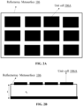
- FIGS. 2A and 2B illustrate an exemplary representation (not to scale) of a top view and a side view, respectively of the reflectarray metasurface 106A comprising arrangement of the plurality of comb-shaped unit cells 106A equally spaced as the matrix, in accordance with some embodiments of the present disclosure.
- the dimensions of the matrix illustrated are representative of an exemplary embodiment, t represents thickness of the first dielectric substrate 106B and ⁇ r represents dielectric constant. Shape and size of plurality of comb-shaped unit cells 106A together with the thickness and the dielectric constant of the first dielectric substrate 106B determine a frequency of operation.
- each of the plurality of comb-shaped unit cells 106A is square shaped with outer dimension being P ⁇ P where P is defined as periodicity, and the shape of the first dielectric substrate an second dielectric substrate are rectrangular.
- the electronic beam-steering reflectarray antenna system 100 further comprises a first dielectric substrate 106B separating a copper bottom layer reflector 106C and the plurality of comb-shaped unit cells 106A, a second dielectric substrate 106D separating the copper bottom layer reflector 106C and an additional copper layer 106E comprising a plurality of copper pads.
- the electronic beam-steering reflectarray antenna system 100 is controlled by a control unit 108.
- the control unit 108 comprises one or more data storage devices or memory 108C configured to store instructions, one or more communication interfaces 108B, and one or more hardware processors 108A operatively coupled to the one or more data storage devices 108C via the one or more communication interfaces 108C, wherein the one or more hardware processors 108A are configured by the instructions to perform beam steering.
- the one or more hardware processors 108A can be implemented as one or more microprocessors, microcomputers, microcontrollers, digital signal processors, central processing units, state machines, logic circuitries, and/or any devices that manipulate signals based on operational instructions.
- the processor(s) 108A is/are configured to fetch and execute computer-readable instructions stored in the memory.
- the expressions 'processors' and ⁇ hardware processors' may be used interchangeably.
- the electronic beam-steering reflectarray antenna system 100 can be implemented in a variety of computing systems, such as laptop computers, notebooks, hand-held devices (e.g., smartphones, tablet phones, mobile communication devices, and the like), workstations, mainframe computers, servers, a network cloud, and the like.
- laptop computers notebooks
- hand-held devices e.g., smartphones, tablet phones, mobile communication devices, and the like
- workstations e.g., smartphones, tablet phones, mobile communication devices, and the like
- mainframe computers e.g., mainframe computers, servers, a network cloud, and the like.
- the communication interface(s) or input/output (I/O) interface(s) 108B can include a variety of software and hardware interfaces, for example, a web interface, a graphical user interface, and the like and can facilitate multiple communications within a wide variety of networks N/W and protocol types, including wired networks, for example, LAN, cable, etc., and wireless networks, such as WLAN, cellular, or satellite.
- the I/O interface device(s) can include one or more ports for connecting a number of devices to one another or to another server.
- the one or more data storage devices or memory 108C may include any computer-readable medium known in the art including, for example, volatile memory, such as static random access memory (SRAM) and dynamic random access memory (DRAM), and/or non-volatile memory, such as read only memory (ROM), erasable programmable ROM, flash memories, hard disks, optical disks, and magnetic tapes.
- volatile memory such as static random access memory (SRAM) and dynamic random access memory (DRAM)
- DRAM dynamic random access memory
- non-volatile memory such as read only memory (ROM), erasable programmable ROM, flash memories, hard disks, optical disks, and magnetic tapes.
- the one or more hardware processors 108A of the control unit 108 configured by instructions to execute an optimization technique for optimizing the design of the first unit cell structure 300 and the second unit cell structure 400 to obtain a plurality of reflection phase responses.
- the one or more hardware processors 108A are configured by the instructions to tilt the reflected beam in the desired direction, from the obtained plurality of reflection phase responses.
- a database 108D is comprised in the memory 108C, wherein the database 108D comprises information on a plurality of parameters corresponding to the plurality of comb-shaped unit cells.
- the memory 108C further includes a plurality of modules (not shown), such modules for various technique(s) such as a Snell's law, a standard Floquet port analysis.
- the above-mentioned technique(s) are implemented as at least one of a logically self-contained part of a software program, a self-contained hardware component, and/or, a self-contained hardware component with a logically self-contained part of a software program embedded into each of the hardware component (e.g., hardware processor 108A or memory 108C) that when executed perform the method described herein.
- the memory 108C further comprises (or may further comprise) information pertaining to input(s)/output(s) of each step performed by the systems and methods of the present disclosure. In other words, input(s) fed at each step and output(s) generated at each step are comprised in the memory 108C and can be utilized in further processing and analysis.
- FIG. 3 illustrates an exemplary design of one type of comb-shaped unit cells referred as the first unit cell structure 300 of the electronic beam-steering reflectarray antenna system 100 with varactor diode embedded comb-shaped unit cell, in accordance with some embodiments of the present disclosure.
- the design of the first unit cell structure 300 comprises a comb-shaped structure with a comb-shaped first part 302 and a comb-shaped second part 304 separated by a predefined gap to mount the varactor diode 306 at a designated position.
- the comb-shaped first part 302 comprises a first trunk 302A, and a plurality of first arms comprises a first top arm 302B, a first center arm 302C and a first bottom arm 302D.
- the comb-shaped second part 304 comprises a second trunk 304A, and a plurality of second arms comprises a second top arm 304B, a second center arm 304C, and a second bottom arm 304D.
- a structural design of the first trunk 302A, the second trunk 304A, the plurality of first arms and the plurality of second arms comprises a copper bottom layer reflector 106C, a first dielectric substrate 106B separating the copper bottom layer reflector 106C and the comb-shaped structure.
- the first trunk 302A and the second trunk 304A have one or more X-directed copper patches, and the plurality of first arms and the plurality of second arms has a single Y-directed copper patche.
- the first trunk 302A spans across length of the comb-shaped unit cell along the X-direction 308.
- the second center arm 304C is of fixed length and connected to the copper bottom layer reflector 106C through the first cylindrical metal post 304, and wherein a DC voltage fed to the varactor diode 306 through the first trunk 302A.
- FIG. 4 illustrates an exemplary design of the second unit cell structure 400 of the electronic beam-steering reflectarray antenna system 100 with varactor diode embedded comb-shaped unit cell, in accordance with some embodiments of the present disclosure.
- the design of the second unit cell structure 400 is a variation to the first unit cell structure 300 with the additional copper layer 106E positioned below the copper bottom layer reflector 106C through a hole 408 with the second cylindrical metal post 406 from the first center arm 302C, a second dielectric substrate 106D separating the copper bottom layer reflector 106C and the additional copper layer 106E, and wherein length of the first trunk 302A is less than length of the comb-shaped unit cell in the X-direction 308.
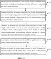
- FIG. 5A depicts flow diagram illustrating a method for optimizing the design of the first unit cell structure 300 and FIGS. 5B and 5C depict a flow diagram illustrating a method for optimizing the design of the second unit cell structure 400 of the electronic beam-steering reflectarray antenna system 100, in accordance with some embodiments of the present disclosure.
- the electronic beam-steering reflectarray antenna system 100 comprises one or more data storage devices or the memory 108C operatively coupled to the one or more hardware processors 108A and is configured to store instructions for execution of steps of the method depicted in FIG 5A and the method depicted in FIGS. 5B and 5C by the one or more processors 108A.
- the one or more hardware processors 108A set, the plurality of parameters of the first unit cell structure 300 as constant values except comb arm length corresponding to the plurality of first arms, the second top arm 304B, and the second bottom arm 304D. Initially the plurality of parameters of the first unit cell structure 300 are fixed to constant values by:
- the plurality of parameters of the first unit cell structure 300 are shown in Table 1.
- Table 1 Parameters Parameter name Dimension Value (mm) Periodicity of the first unit cell structure P 5.3 Width of the first trunk and the second trunk Wt 0.3 Comb arm length of the plurality of first arms, second top arm, second bottom arm La variable Width of plurality of first arms and plurality of second arms Wa 0.2 Comb arm span Ls 2 Gap between comb-shaped first part and Comb-shaped second part G 0.4 Pad for shorting cylindrical metal post pad 0.6 Diameter of shorting cylindrical metal post -- 0.5 first dielectric substrate thickness t 0.787 first dielectric substrate constant ⁇ r 2.2
- FIGS. 6A and 6B illustrates an exemplary representation of a top view and a side view, respectively of the first unit cell structure 300 of the electronic beam-steering reflectarray antenna system with varactor diode embedded comb shaped unit cell. More specifically dimension values in the top view and the side view, respectively of the first unit cell structure 300 are represented in FIGS. 6A and 6B , in accordance with some embodiments of the present disclosure.
- the one or more hardware processors 108A obtain, a plurality of frequency variations of an incident electromagnetic wave and a corresponding plurality of reflection phase responses of the reflected beam, without mounting the varactor diode 306 on the first unit cell structure 300, for a plurality of comb arm length variations, over a mode1 simulation and a mode2 simulation.
- the comb arm length varies between first value and a second value by steps of a predefined value. Varying the comb arm length enables the plurality of frequency variations between a first frequency value and a second frequency value of the electromagnetic wave incident on the first unit cell structure.
- a standard Floquet port analysis is conducted for the first unit cell structure 300 where the comb arm length is varied from 0.5mm to 1.5mm in steps of 0.05mm, in accordance with some embodiments of the present disclsoure. Further model simualtion and the mode2 simulation is perfrormed for each of the comb arm length.
- the mode1 simulation comprises field lines of the electromagnetic wave incident parallel to the first trunk 302A, and wherein the mode2 simulation comprises the field lines of the electromagnetic wave incident parallel to the plurality of first arms.
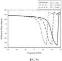
- FIGS. 7A and 7B illustrates mode1 simulation and mode2 simulation, respectively of the first unit cell structure, without mounting the varactor diode, for a plurality of comb arm length variations, in accordance with some embodiments of the present disclosure. More specifically FIGS. 7A , and 7B illustrate a graph plotted for the plurality of frequency variations against the plurality of reflection phase responses for the plurality of comb arm length variations in the model simulation and mode2 simulation. It is observed from FIG. 7A in the graph that as the comb arm length increases the plurality of reflection phase responses versus the frequency of operation curve in the mode1 simulation shifts towards left, that is towards lower frequency. The plurality of reflection phase responses is represented as reflection phase and the frequency of operation is represented as frequency in FIGS.
- Range of the plurality of reflection phase responses that can be attained in the mode1 simulation for a given value of the comb arm length is approximately 330 degrees.
- reflection phase responses change per unit frequency of operation change is high which signifies that the reflectarray metasurface 106 designed with the pluarlity of parameters will be narrowband in terms of the frequency of operation.
- FIG. 7B displays the plurality of reflection phase responses change linearly with the plurality of frequency variations over a smaller phase change of 80 degrees, in the mode2 simulation, for the plurality of comb arm length variations. Therefore, for the plurality of parameters given in the Table 1, mode2 simulation based reflectarray metasurface 106 provides wider bandwidth.
- the one or more hardware processors 108A Upon obtaining the plurality of frequency variations of the incident electromagnetic wave, at step 506 of the present disclosure, the one or more hardware processors 108A obtain, an optimum comb arm length among the plurality of comb arm length variations from one of the mode1 simulation and the mode2 simulation, where the reflection phase response of the plurality of reflection phase responses greater than a predefined reflection phase and for a desired frequency of operation of the plurality of frequency variations.
- the comb arm length 1.15mm is obtianed as the optimum comb arm length among the plurality of comb arm length variations, in accordance with some embodiments of the present disclosure.
- the one or more hardware processors 108A mount, the varactor diode 306 across the predefined gap between the comb-shaped first part 302 and the comb-shaped second part 304.
- the one or more hardware processors 108A Upon mounting the varactor diode 306, at step 510 of the present disclosure, the one or more hardware processors 108A obtain, the plurality of reflection phase responses, for each of the plurality of capacitance values of the DC voltage of the varactor diode 306, for the obtained optimum comb arm length and the desired frequency of operation.
- the first unit cell structure 300 is again simulated with the obtained optimum comb arm length 1.15mm at the desired frequecy of opeation 27GHz, for each of the plurality of capacitance values, by placing the varactor diode 306 at the designated position, in accordance with some embodiments of the present disclosure.
- FIGS. 8A , and 8B illustrates mode1 simulation and mode2 simulation, respectively of the first unit cell structure, by mounting a varactor diode 306, for an obtained optimum comb arm length and the desired frequency of operation, in accordance with some embodiments of the present disclosure. More specifically FIGS. 8A and 8B illustrate, the plurality of reflection phase responses for each of the plurality of capacitance values of the DC voltage of the varactor diode 306, for the optimum comb arm length 1.15mm at the desired frequecy of opeation 27GHz, in accordance with some embodiments of the present disclosure.
- the plurality of reflection phase responses is represented as reflection phase and the plurality of capacitance values is represented as capacity in FIGS. 8A , and 8B .
- the reflectarray metasurface 106 is build using the plurality of comb-shaped unit cells designed as the first unit cell structure 300 with the optimum comb arm length 1.15mm, the desired frequency of operation 27GHz, and the plurality of reflection phase responses obtianed form the mode2 simulation, in accordance with some embodiments of the present disclosure.
- the one or more hardware processors 108A set, the plurality of parameters of the second unit cell structure 400 as constant values except comb arm length corresponding to the plurality of first arms, the second top arm 304B, the second bottom arm 304D, and length of the first trunk 302A.
- the plurality of parameters of the second unit cell structure 400 are shown in Table 2.
- Table2 Parameter parameter name Dimension value (mm) Periodicity of the second unit cell P 5.3 Width of First trunk and the second trunk Wt 0.3 Length of the first trunk LtA variable Length of plurality of first arms, second top arm, second bottom arm La variable Width of the plurality of first arms and the plurality of second arms Wa 0.2 Comb arm span Ls 2 Gap between Comb-shaped First part and Comb-shaped second part G 0.4 Pad for shorting cylindrical metal post pad 0.6 Diameter of shorting cylindrical metal post -- 0.5 Hole diameter in Copper Bottom Layer Reflector - 1 first dielectric substrate thickness t 0.787 first dielectric substrate constant ⁇ r 2.2 Second dielectric Substrate thickness t 0.787 Second dielectric Substrate constant ⁇ r 2.2
- FIGS. 9A , and 9B illustrates an exemplary representation of a top view and a side view, respectively of the second unit cell structure of the electronic beam-steering reflectarray antenna system with varactor diode embedded comb-shaped unit cell, in accordance with some embodiments of the present disclosure. More specifically dimension values of the top view and the side view, respectively of the second unit cell structure 400 are represented in FIGS. 9A , and 9B , in accordance with some embodiments of the present disclosure.
- the one or more hardware processors 108A Upon setting the plurality of parameters of the second unit cell structure 400, at step 514 of the present disclosure, the one or more hardware processors 108A obtain, the plurality of frequency variations of the incident electromagnetic wave and the corresponding plurality of reflection phase responses of the reflected beam, without mounting the varactor diode 306 on the second unit cell structure 400, for the plurality of comb arm length variations.
- the comb arm length varies between the first value and the second value by steps of the predefined value. Initially length of the first trunk 302A is initialized with length of the comb-shaped unit cell.
- a standard Floquet port analysis is conducted for the second unit cell structure 400 where the comb arm length is varied from 0.5mm to 1.5mm in steps of 0.05mm, in accordance with some embodiments of the present disclsoure. Further the mode1 simualtion and the mode2 simulation is perfrormed for each of the plurality of comb arm length variations, and a plurality of comb trunk length variations.
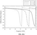
- FIGS. 10A , and 10B illustrates mode1 simulation and mode2 simulation, respectively of the second unit cell structure 400, without mounting the varactor diode, for the plurality of comb arm length variations, in accordance with some embodiments of the present disclosure. More specifically FIGS. 10A , and 10B illustrate a graph plotted for the plurality of frequency variations against the plurality of reflection phase responses for the plurality of comb arm length variations in the model simulation and mode2 simulation. FIGS. 10A , and 10B display results for the model simulation and the mode2 simulation, where the length of the first trunk 302A is kept fixed, and the comb arm length is varied from 0.5mm to 1.5mm in steps of 0.05mm. The plurality of reflection phase responses is represented as the reflection phase and the frequency of operation is represented as the frequency in FIGS. 10A and 10B .
- the one or more hardware processors 108A obtain, the optimum comb arm length among the plurality of comb arm length variations from one of the mode1 simulation and the mode2 simulation, where the reflection phase response of the plurality of reflection phase responses greater than the predefined reflection phase and for the desired frequency of operation of the plurality of frequency variations.
- the comb arm length 1.2mm is obtained as the optimum comb arm length among the plurality of comb arm length variations, in accordance with some embodiments of the present disclosure.
- the one or more hardware processors 108A obtain, the plurality of frequency variations of the incident electromagnetic wave and the corresponding plurality of reflection phase responses of the reflected beam, without mounting the varactor diode 306 on the second unit cell structure 400, for the plurality of comb trunk length variations, wherein the comb trunk length varies between a first trunk length value and a second trunk length value by steps of the predefined value.
- the comb arm length here is set to the optimum comb arm length, in accordance with some embodiments of the present disclosure.
- the one or more hardware processors 108A obtain, the optimum comb trunk length among the plurality of comb trunk length variations from one of the mode1 simulation and the mode2 simulation, where the reflection phase response of the plurality of reflection phase responses greater than the predefined reflection phase for the desired frequency of operation of the plurality of frequency variations.
- the one or more hardware processors 108A mount, the varactor diode 306 across the predefined gap between the comb-shaped first part 402 and the comb-shaped second part 404.
- the one or more hardware processors 108A obtain, the plurality of reflection phase responses, for each of the plurality of capacitance values of the DC voltage of the varactor diode, for the obtained optimum comb arm length, the optimum comb trunk length, and the desired frequency of operation.
- the second unit cell structure 400 is again simulated with the obtained optimum comb arm length 1.2mm, the optimum comb trunk length 3mm at the desired frequecy of opeation 27GHz, for each of the plurality of capacitance values, by placing the varactor diode 306 at the designated position, in accordance with some embodiments of the present disclosure.
- the reflectarray metasurface 106 is build using the plurality of comb-shaped unit cells designed as the second unit cell structure 400 with the optimum comb arm length 1.2mm, the optimum comb trunk length 3mm, the desired frequency of operation 27GHz, and the plurality of reflection phase responses obtianed form the mode1 simulation, in accordance with some embodiments of the present disclosure.
- FIG. 11 illustrates a mode1 simulation of the second unit cell structure, by mounting the varactor diode 306, for the optimum comb arm length and the optimum comb trunk length, the desired frequency of operation, in accordance with some embodiments of the present disclosure.
- the plurality of reflection phase responses is represented as reflection phase and the plurality of capacitance values is represented as capacity in FIG. 11 .
- the reflection phase undergoes approximately 330 degrees twice in selected capacity range between 200fF to 900fF. This signifies that any specific reflection phase response corresponds to two possible capacitance values which in turn relates to two DC bias options.
- the reflection phase gradient of the reflectarray meta surface 106 is obtained from the plurality reflection phase responses corresponding to each of the plurality of comb-shaped unit cells 106A, designed as one of the first unit cell structure 300 and the second unit cell structure 400, for a desired angle received from a user.
- the obtained plurality of capacitance values is mapped to the DC bias voltages corresponding to the varactor diodes 306 using a predefined lookup table. Suitable DC bias voltage is applied to the varactor diode in each of the plurality of comb-shaped unit cells 106A, to tilt the reflected beam over the desired direction.
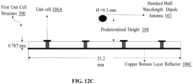
- FIGS. 12A , 12B , and 12C illustrates an exemplary representation of a top view and a side view, and a front view respectively of the reflectarray metasurface 106 comprising the plurality of comb-shaped unit cells of the first unit cell structure 300, in accordance with some embodiments of the present disclosure.
- Each of the plurality of comb-shaped unit cells 106A are mounted with the varactor diode 306 with a predefined capacitance value.
- the standard half-wavelength dipole antenna 102 is placed at the predetermined height 104 above the refelctarray metasurface 106. Dipole arms of the standard half-wavelength dipole antenna 102 are oriented accordingingly to the mode2 simulation. Specifically FIGS.
- FIG. 12A illustrates an exemplary representation of the plurality of comb-shaped unit cells 106A arranged as the matrix of 6 columns and 4 rows over the reflectarray metasurface 106.
- the plurality of the comb-shaped unit cells 106A in each of the column have same capacitance values. This is due to the reason reverse bias to the varactor diode 306 are fed through the first trunk 302A which is common for all the plurality of comb-shaped unit cells 106A in each of the column.
- different capacitance values are fed across the 6 columns resulting in a reflection phase gradient towards the +Y axis.
- the first row in the Table. 3 represents the different capacitance values fed across the 6 columns and the second row of Table 3 depicts the corresponding reflection phase responses.
- Table. 3 Capacitor (fF) 700 760 801 873 253 355 Reflection Phase (deg) 153.57 127.58 102.94 77.18 50.67 24.52
- Table. 4 illustrates beam tilt angles for different heights of the standard half-wavelength dipole antenna 102 over the reflectarray metasurface 106.
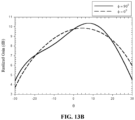
- the beam-steering angle is stable between 7.5° and 8.6° for the frequency of the operation between 26.8GHz and 27.2GHz.
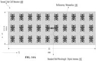
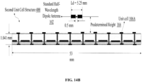
- FIGS. 14A , 14B , and 14C illustrates an exemplary representation of a top view and a side view, and a front view respectively of the reflectarray metasurface 106 comprising a plurality of comb-shaped unit cells of the second unit cell structure, in accordance with some embodiments of the present disclosure.
- Each of the plurality of comb-shaped unit cells are mounted with the varactor diode 306 with the predefined capacitance value.
- the standard half-wavelength dipole antenna 102 is placed at the predetermined height above the refelctarray metasurface 106 is used to excite the the refelctarray metasurface 106.
- the dipole arms of the standard half-wavelength dipole antenna are oriented accordingingly to the mode1 simulation. Specifically FIGS.
- FIG. 14A illustrates an exemplary representation of the plurality of comb-shaped unit cells 106A arranged as a matrix of 10 columns along X-axis and 3 rows along Y-axis over the reflectarray metasurface. It is assumed that the plurality of comb-shaped unit cells 106A for each of the coloumn have identical capacitance values whereas the plurlaity of comb-shaped unit cells 106A across the coloumns have the phase gradient. Thus the beam-steering will take place only in the X-Z plane. For evaluating the beam steeering, different capacitance values are fed across the 10 columns resulting in the refelction reflection phase gradient towards +X axis, shown in Table. 6.
- the first column in the Table. 6 represents the different capacitance values fed across the 10 columns and the corresponding reflection phase responses.
- Table. 6 Capacitor (fF) Reflection phase (deg) 150 162.77 252 142.84 269 123.01 276 103.04 280 81.23 282 65.55 284 34.37 286 17.12 286 3.56 289 -30.71
- FIGS. 15A , and 15B illustrates an exemplary representation (not to scale) of radiation gain pattern corresponding to the beam steering of the reflectarray metasurface created by using plurality of comb-shaped unit cells of second unit cell structure 400, in accordance with some embodiments of the present disclosure, in accordance with some embodiments of the present disclosure.
- FIG. 15A represents the radiation gain pattern for X-Z plane and Y-Z plane, for the standard half-wavelength dipole antenna 102 placed at the height 7.9mm above the reflectarray metasurface.
- Table. 7 illustrates beam tilt angles for different heights of the standard half-wavelength dipole antenna 102 over the reflectarray metasurface 106.
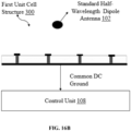
- FIGS. 16A , and 16B illustrates a schematic diagram of a top view and a side view, respectively for feeding the DC bias voltage to the varactor diode 306, for beam steering the reflectarrray metasurface 106 created by using the plurality of comb-shaped unit cells 106A of first unit cell structure 300, in accordance with some embodiments of the present disclosure.
- specific DC reverse bias voltages are fed to the varactor diode 306 embedded in each of the plurality of comb-shaped unit cells 106A.
- the DC revere bias voltages are fed from a microcontroller-based control unit to the columns through direct connect to the first trunk 302A.
- the DC return path from the microcontroller-based control unit is connected to the copper bottom layer reflector 106C.
- the DC reverse bias voltage setting is user configurable.
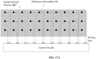
- FIGS. 17A , and 17B illustrates a schematic diagram of a top view and a side view, respectively for feeding the DC bias voltage to the varactor diode 306, for beam steering the reflectarrray metasurface 106 created by using the plurality of comb-shaped unit cells 106A of the second unit cell structure 400, in accordance with some embodiments of the present disclosure.
- specific DC reverse bias voltages are fed to the varactor diode 306 embedded in each of the plurality of comb-shaped unit cells 106A.
- the DC return path is connected to the copper bottom layer reflector 106C and each copper patch in the additional copper layer 106Eis individually fed with reconfigurable DC bias.
- the reflectarray metasurface 106 constructed with the plurality of comb-shaped unit cells of the first unit cell structure 300 can perform the beam steering only in one plane.
- the reflectarray metasurface 106 constructed with the plurality of comb-shaped unit cells of the second unit cell structure 400 can perform the beam steering simultaneously along both orthogonal planes.
- the present disclosure herein addresses design of the plurality of comb-shaped unit cells 106A arranged over the reflectarray metasurface 106.
- the plurality of comb-shaped unit cells 106A is designed as one of (i) the first unit cell structure 300 and (ii) the second unit cell structure 400 and further optimized by using the optimization technique. Further the standard half-wavelength dipole antenna 102 is integrated with the proposed reflectarray metasurface 106 to produce electronically steerable antenna in the desired direction.
- Such computer-readable storage means contain program-code means for implementation of one or more steps of the method, when the program runs on a server or mobile device or any suitable programmable device.
- the hardware device can be any kind of device which can be programmed including e.g., any kind of computer like a server or a personal computer, or the like, or any combination thereof.
- the device may also include means which could be e.g., hardware means like e.g., an application-specific integrated circuit (ASIC), a field-programmable gate array (FPGA), or a combination of hardware and software means, e.g., an ASIC and an FPGA, or at least one microprocessor and at least one memory with software processing components located therein.
- the means can include both hardware means and software means.
- the method embodiments described herein could be implemented in hardware and software.
- the device may also include software means. Alternatively, the embodiments may be implemented on different hardware devices, e.g., using a plurality of CPUs.
- the embodiments herein can comprise hardware and software elements.
- the embodiments that are implemented in software include but are not limited to, firmware, resident software, microcode, etc.
- the functions performed by various components described herein may be implemented in other components or combinations of other components.
- a computer-usable or computer readable medium can be any apparatus that can comprise, store, communicate, propagate, or transport the program for use by or in connection with the instruction execution system, apparatus, or device.
- a computer-readable storage medium refers to any type of physical memory on which information or data readable by a processor may be stored.
- a computer-readable storage medium may store instructions for execution by one or more processors, including instructions for causing the processor(s) to perform steps or stages consistent with the embodiments described herein.
- the term "computer-readable medium” should be understood to include tangible items and exclude carrier waves and transient signals, i.e., be non-transitory. Examples include random access memory (RAM), read-only memory (ROM), volatile memory, nonvolatile memory, hard drives, CD ROMs, DVDs, flash drives, disks, and any other known physical storage media.
Landscapes
- Physics & Mathematics (AREA)
- Electromagnetism (AREA)
- Optics & Photonics (AREA)
- Aerials With Secondary Devices (AREA)
- Variable-Direction Aerials And Aerial Arrays (AREA)
Abstract
Description
- The present application claims priority to
Indian provisional patent application no. 202321032134 filed on May 05, 2023 - The disclosure herein generally relates to the field of antenna based reflect array system, and, more particularly, to electronic beam-steering reflectarray antenna system with varactor diode embedded comb-shaped unit cell.
- Globally, major initiative is ongoing to build components, sub-systems and systems for 5th generation (5G) millimeter wave Frequency Range 2 (FR2) band which offers many advantages. Some of its advantages are high data rate, ultra-high throughput, low latency and thereof. The abundant spectrum available at (5G) millimeter wave FR2 band (24GHz+) make it an ideal candidate for various applications where electronically beam steered antenna is the critical component. Now-a-days a phased antenna array is the most prevalent technology used for beam steering antenna. Here the beam steering is achieved by establishing a reflection phase gradient across all antenna elements using digital phase shifters. For large, phased antenna arrays where large aperture size gives narrow beamwidth, the overall cost and the size for the beam steering may become too expensive. The phased antenna arrays consist of multiple antenna elements, wherein each antenna element is fed with different phase shifts to tilt the resultant beam in a desired direction. The main challenge in this type of architecture is that there must be a separate phase shifters network with many phase shifters. Further the phase shifters increase cost and complexity of the system.
- To eliminate the usage of phase shifters, reconfigurable metasurfaces of different designs are utilized either with varactor diode or Positive-Intrinsic-Negative (PIN) diodes as a potential alternative approach. Metasurfaces are two-dimensional (2D) version of metamaterials with negligible thickness comprising several unit cells of sub-wavelength dimensions, arranged periodically over a substrate surface. The varactor diodes are placed in each of the unit cells in such a way to provide it with the direct current (DC) biasing network. Depending on proper size, orientation, and arrangement of the unit cell, the metasurface can transmit, reflect, or absorb an electromagnetic beam.
- A tunable metasurface-based flat panel reflector with the integrated varactor diode or the PIN diode has been studied in recent times and different new designs of the same are explored. However, new designs which relate to a novel unit cell structures have continuously been explored for the purpose of higher frequency of operation, higher radiation efficiency, and higher frequency bandwidth, higher directivity, high efficiency, low profile, and ease of setting beam tilt angle with precision. Also, a precise technique of synthesizing and evaluating new unit cells is needed.
- In metasurface based beam-steering antennas, the reflection phase gradient required for a desired beam tilt angle is computed using generalized Snell's law. Theoretically it is possible to obtain the required inter-element refection phase gradient by changing capacitance values embedded in each unit cell. But the implementation becomes significantly challenging since the reflection phase gradient rapidly changes with small changes in the capacitance values. Moreover, for wide beam tilt angle the reflection phase gradient need to cover entire range of 0 degree to 360 degree. However, there isn't any standard way to achieve the wide beam tilt angle to cover entire range of 0 degree to 360 degree for better designing the metasurface based beam-steering antennas.
- Embodiments of the present disclosure present technological improvements as solutions to one or more of the above-mentioned technical problems recognized by the inventors in conventional systems.
- In an aspect, there is provided an electronic beam-steering reflectarray antenna system with varactor diode embedded comb-shaped unit cell comprising: a reflectarray metasurface positioned at a predetermined height below a standard half-wavelength dipole antenna; a plurality of comb-shaped unit cells arranged as a matrix over the reflectarray metasurface, wherein each of the plurality of comb-shaped unit cells is designed as one of (i) a first unit cell structure and (ii) a second unit cell structure, and wherein the first unit cell structure comprising: a comb shaped structure with a comb shaped first part and a comb shaped second part separated by a predefined gap to mount a varactor diode at a designated position, wherein the comb shaped first part comprising a first trunk, and a plurality of first arms comprising a first top arm, a first center arm and a first bottom arm, wherein the comb shaped second part comprising a second trunk, and a plurality of second arms comprising a second top arm, a second center arm, and a second bottom arm, and a structural design of the first trunk, the second trunk, the plurality of first arms and the plurality of second arms comprising a copper bottom layer reflector, a first dielectric substrate separating the copper bottom layer reflector and the comb shaped structure, wherein the first trunk and the second trunk has one or more X-directed copper patches, and the plurality of first arms and the plurality of second arms has a single Y-directed copper patches, wherein the first trunk spans across length of the comb-shaped unit cell along the X-direction, wherein the second center arm is of fixed length and connected to the copper bottom layer reflector through the first cylindrical metal post, and wherein a DC voltage fed to the varactor diode through the first trunk.
- In accordance with an embodiment of the present disclosure, the design of the second unit cell structure comprising: a variation to the first unit cell structure with an additional copper layer positioned below the copper bottom layer reflector through a hole with the second cylindrical metal post from the first center arm, a second dielectric substrate separating the copper bottom layer reflector and the additional copper layer, and wherein length of the first trunk is less than length of the comb-shaped unit cell structure in the X-direction.
- In accordance with an embodiment of the present disclosure, the electronic beam-steering reflectarray antenna system is controlled by a control unit comprising one or more hardware processors, coupled to a memory via one or more communication interfaces.
- In accordance with an embodiment of the present disclosure, the one or more hardware processors are configured by the instructions to tilt the reflected beam in a desired direction, from the obtained plurality of reflection phase responses by: identifying, a reflection phase gradient of the reflectarray meta surface, from a plurality reflection phase responses corresponding to each of the plurality of unit cells for a desired angle received from a user; obtaining, a capacitance value of a plurality of capacitance values, for each of the plurality of unit cells, from the reflection phase gradient; mapping, the obtained plurality of capacitance values to the DC voltages corresponding to the varactor diodes using a predefined lookup table; and applying, suitable DC voltage to the varactor diode in each of the plurality of unit cells, to tilt the reflected beam over a desired direction.
- In another aspect, a method for optimizing design of a first unit cell structure and a second unit structure is provided. The method includes optimizing, via an optimization technique executed by one or more hardware processors of a control unit controlling an electronic beam-steering reflectarray antenna system, a design of one of (i) a first unit cell structure and (ii) a second unit cell structure of a comb shaped unit cell of the electronic beam-steering reflectarray antenna system.
- In accordance with an embodiment of the present disclosure, the optimization technique for optimizing the design of the first unit cell structure comprising: performing simulation comprising a mode1 simulation and a mode2 simulation on the first unit cell structure to (i) obtain an optimum comb arm length corresponding to the plurality of first arms, the second top arm, and the second bottom arm and (ii) estimate a plurality of reflection phase responses by: (a) setting a plurality of parameters of the first unit cell structure as constant values except comb arm length corresponding to the plurality of first arms, the second top arm, and the second bottom arm; (b) obtaining a plurality of frequency variations of an incident electromagnetic wave and a corresponding plurality of reflection phase responses of a reflected beam, without mounting the varactor diode on the first unit cell structure, for a plurality of comb arm length variations, wherein the comb arm length varies between first value and a second value by steps of a predefined value, wherein varying the comb arm length enables the plurality of frequency variations between a first frequency value and a second frequency value of the electromagnetic wave incident on the first unit cell structure, wherein the mode1 simulation comprises field lines of an electromagnetic wave incident parallel to the first trunk, and wherein the mode2 simulation comprises the field lines of the electromagnetic wave incident parallel to the plurality of first arms; (c) obtaining, the optimum comb arm length among the plurality of comb arm length variations from one of (i) the mode1 simulation and (ii) the mode2 simulation with a reflection phase response of the plurality of reflection phase responses greater than a predefined reflection phase and for a desired frequency of operation of the plurality of frequency variations; (d) mounting the varactor diode across the predefined gap between the comb shaped first part and the comb shaped second part; and (e) obtaining, the plurality of reflection phase responses, for each of the plurality of capacitance values of the DC voltage of the varactor diode, for the obtained optimum comb arm length and the desired frequency of operation.
- In accordance with an embodiment of the present disclosure, the optimization technique for optimizing the design of the second unit cell structure comprising: performing simulation comprising mode1 simulation and a mode2 simulation on the second unit cell structure, (i) to obtain the optimum comb arm length corresponding to the plurality of first arms, the second top arm, and the second bottom arm and an optimum comb trunk length corresponding to the first trunk, and (ii) to estimate the plurality of reflection phase responses by: (a) setting the plurality of parameters of the second unit cell structure as constant values except the comb arm length corresponding to the plurality of first arms, the second top arm, and the second bottom arm, and length of the first trunk; (b) obtaining the plurality of frequency variations of an incident electromagnetic wave and the corresponding plurality of reflection phase responses of the reflected beam, without mounting the varactor diode on the second unit cell structure, for the plurality of comb arm length variations, wherein the comb arm length varies between first value and a second value by steps of a predefined value, wherein initially the length of the first trunk initialized with length of the comb-shaped unit cell; (c) obtaining, the optimum comb arm length among the plurality of comb arm length variations from one of (i) the mode1 simulation and (ii) the mode2 simulation, where the reflection phase response of the plurality of reflection phase responses greater than the predefined reflection phase and for the desired frequency of operation of the plurality of frequency variations; (d) obtaining the plurality of frequency variations of an incident electromagnetic wave and the corresponding plurality of reflection phase responses of the reflected beam, without mounting the varactor diode on the second unit cell structure, for the plurality of comb trunk length variations, wherein the comb trunk length varies between a first trunk length value and a second trunk length value by steps of the predefined value; (e) obtaining, the optimum comb trunk length among the plurality of comb trunk length variations from one of (i) the mode1 simulation and (ii) the mode2 simulation, where the reflection phase response of the plurality of reflection phase responses greater than the predefined reflection phase for the desired frequency of operation of the plurality of frequency variations; (f) mounting the varactor diode across the predefined gap between the comb shaped first part and the comb shaped second part; and (g) obtaining, the plurality of reflection phase responses, for each of the plurality of capacitance values of the DC voltage of the varactor diode, for the obtained optimum comb arm length, the optimum comb trunk length, and the desired frequency of operation.
- In accordance with an embodiment of the present disclosure, the one or more hardware processors are configured by the instructions to tilt the reflected beam in a desired direction, from the obtained plurality of reflection phase responses by: identifying, a reflection phase gradient of the reflectarray meta surface, from a plurality reflection phase responses corresponding to each of the plurality of unit cells for a desired angle received from a user; obtaining, a capacitance value of a plurality of capacitance values, for each of the plurality of unit cells, from the reflection phase gradient; mapping, the obtained plurality of capacitance values to the DC voltages corresponding to the varactor diodes using a predefined lookup table; and applying, suitable DC voltage to the varactor diode in each of the plurality of unit cells, to tilt the reflected beam over the desired direction.
- In yet another aspect, there are provided one or more non-transitory machine-readable information storage mediums comprising one or more instructions which when executed by one or more hardware processors cause a method for optimizing design of a first unit cell structure and a second unit structure is provided. The method includes optimizing, via an optimization technique executed by one or more hardware processors of a control unit controlling an electronic beam-steering reflectarray antenna system, a design of one of (i) a first unit cell structure and (ii) a second unit cell structure of a comb shaped unit cell of the electronic beam-steering reflectarray antenna system.
- It is to be understood that both the foregoing general description and the following detailed description are exemplary and explanatory only and are not restrictive of the invention, as claimed.
- The accompanying drawings, which are incorporated in and constitute a part of this disclosure, illustrate exemplary embodiments and, together with the description, serve to explain the disclosed principles:
-
FIG. 1 illustrates an exemplary block diagram of an electronic beam-steering reflectarray antenna system with varactor diode embedded comb-shaped unit cell, in accordance with some embodiments of the present disclosure. -
FIGS. 2A, and 2B illustrate an exemplary representation (not to scale) of a top view and a side view, respectively of a reflectarray metasurface comprising arrangement of a plurality of comb-shaped unit cells equally spaced as a matrix, in accordance with some embodiments of the present disclosure. -
FIG. 3 illustrates an exemplary design of one type of comb-shaped unit cells referred as a first unit cell structure of the electronic beam-steering reflectarray antenna system with varactor diode embedded comb-shaped unit cell, in accordance with some embodiments of the present disclosure. -
FIG. 4 illustrates an exemplary design of another type of comb-shaped unit cells referred as a second unit cell structure of the electronic beam-steering reflectarray antenna system with varactor diode embedded comb-shaped unit cell, in accordance with some embodiments of the present disclosure. -
FIG. 5A depicts flow diagram illustrating a method for optimizing the design of the first unit cell structure andFIGS. 5B , and5C depict a flow diagram illustrating a method for optimizing the design of the second unit cell structure of the electronic beam-steering reflectarray antenna system, in accordance with some embodiments of the present disclosure. -
FIGS. 6A , and6B illustrates an exemplary representation of a top view and a side view, respectively of the first unit cell structure of the electronic beam-steering reflectarray antenna system with varactor diode embedded comb-shaped unit cell, in accordance with some embodiments of the present disclosure. -
FIGS. 7A , and7B illustrates mode1 simulation and mode2 simulation, respectively of the first unit cell structure, without mounting a varactor diode, for a plurality of comb arm length variations, in accordance with some embodiments of the present disclosure. -
FIGS. 8A , and8B illustrates mode1 simulation and mode2 simulation, respectively of the first unit cell structure, by mounting the varactor diode, for an obtained optimum comb arm length and a desired frequency of operation, in accordance with some embodiments of the present disclosure. -
FIGS. 9A , and9B illustrates an exemplary representation (not to scale) of a top view and a side view, respectively of the second unit cell structure of the electronic beam-steering reflectarray antenna system with varactor diode embedded comb-shaped unit cell, in accordance with some embodiments of the present disclosure. -
FIGS. 10A , and10B illustrates mode1 simulation and mode2 simulation, respectively of the second unit cell structure, without mounting the varactor diode, for the plurality of comb arm length variations, in accordance with some embodiments of the present disclosure. -
FIG. 11 illustrates a mode1 simulation of the second unit cell structure, by mounting the varactor diode, for the optimum comb arm length and the optimum comb trunk length, the desired frequency of operation, in accordance with some embodiments of the present disclosure. -
FIGS. 12A ,12B , and12C illustrates an exemplary representation (not to scale) of a top view, a side view, and a front view respectively of the reflectarray metasurface comprising the plurality of comb-shaped unit cells of the first unit cell structure, in accordance with some embodiments of the present disclosure. -
FIGS. 13A , and13B illustrates an exemplary representation of radiation gain pattern corresponding to beam steering of the reflectarray metasurface created by using the plurality of comb-shaped unit cells of the first unit cell structure, in accordance with some embodiments of the present disclosure. -
FIGS. 14A ,14B , and14C illustrates an exemplary representation (not to scale) of a top view and a side view, and a front view respectively of the reflectarray metasurface comprising the plurality of comb-shaped unit cells of the second unit cell structure, in accordance with some embodiments of the present disclosure. -
FIGS. 15A , and15B illustrates an exemplary representation of radiation gain pattern corresponding to the beam steering of the reflectarray metasurface created by using the plurality of comb-shaped unit cells of second unit cell structure, in accordance with some embodiments of the present disclosure. -
FIGS. 16A , and16 B illustrates a schematic diagram of a top view and a side view, respectively for feeding the DC bias voltage to the varactor diode, for beam steering the reflectarrray metasurface created by using the plurality of comb-shaped unit cells of the first unit cell structure, in accordance with some embodiments of the present disclosure. -
FIGS. 17A , and17B illustrates a schematic diagram of a top view and a side view, respectively for feeding the DC bias voltage to the varactor diode, for beam steering the reflectarrray metasurface created by using the plurality of comb-shaped unit cells of the second unit cell structure, in accordance with some embodiments of the present disclosure. - Exemplary embodiments are described with reference to the accompanying drawings. In the figures, the left-most digit(s) of a reference number identifies the figure in which the reference number first appears. Wherever convenient, the same reference numbers are used throughout the drawings to refer to the same or like parts. While examples and features of disclosed principles are described herein, modifications, adaptations, and other implementations are possible without departing from the scope of the disclosed embodiments. It is intended that the following detailed description be considered as exemplary only, with the true scope being indicated by the following embodiments described herein.
- For better designing of metasurface based beam-steering antennas, size, shape, and periodicity of a plurality of comb-shaped unit cells and a corresponding plurality of refection phase responses of the plurality of comb-shaped unit cells need to be investigated.
- The present disclosure optimizes design of the plurality of comb-shaped unit cells arranged over a reflectarray metasurface. The plurality of comb-shaped unit cells is designed as one of (i) a first unit cell structure and (ii) a second unit cell structure. Moreover, a standard half-wavelength dipole antenna is integrated with the proposed reflectarray metasurface to produce electronically steerable antenna. The reflectarray metasurface is positioned at a predetermined height below the standard half-wavelength dipole antenna. Each of the plurality of comb-shaped unit cell is embedded with a commercially available varactor diode. These varactor diodes, when driven by appropriate direct current (DC) biasing voltages offer different capacitance values.
- If each of the plurality of comb-shaped units cell gets different DC bias voltages, then the reflectarray metasurface gets transformed to a programmable structure whose reflection phase gradient can be adjusted which in turn helps in tilting a reflected beam over a desired direction. The DC bias voltage adjustment is controlled digitally where the user feeds the desired angle which leads to computing the necessary reflection phase gradient (Generalized Snell's law) followed by selecting necessary capacitance values and the corresponding DC bias voltages for each of the plurality of comb-shaped unit cells. The plurality of comb-shaped unit cells designed as the first unit cell structure helps in tilting the reflected beam over the desired direction in a single line. The plurality of comb-shaped unit cells designed as the second unit cell structure helps in tilting the reflected beam over the desired direction in a two-dimensional (2D) plane.
- In the context of the subject disclosure, definitions of certain expressions and their usage are as explained herein below.
- Metamaterials are artificial structures consisting of periodic inclusions or unit cells that show exotic properties. The precise geometry, size and orientation of the unit cell structures render them capable of manipulating electromagnetic waves, like blocking, absorbing, enhancing, or bending the electromagnetic waves. Potential applications of the metamaterials include high efficiency absorbers/rasorbers, invisibility cloaks, medical devices and thereof.
- Metasurfaces are planar metamaterials with subwavelength thickness comprised of single-layer or multi-layer planar structures which can be readily fabricated using cost-effective methods like nano-printing. In recent times, metasurfaces, the two-dimensional counterpart of metamaterials, provide an alternative scheme to manipulate the electromagnetic waves by arranging the artificial structures on a flat interface to engineer the phase profile, polarization, amplitude, and trajectory of electromagnetic waves. The subwavelength thickness, low loss, and easy fabrication can be exhibited for the planar metasurfaces. Hence, it is important to develop novel metasurfaces for controlling the electromagnetic waves. The metasurfaces are ultra-thin, low-cost, easily fabricated structures that are used when low-profile structures are needed. The metasurfaces provide a planar surface with surface impedance which can be specially designed to be manipulated by electronic means and can control the phase and group velocities of plane waves for wave-front engineering, polarization control, cloaking, scatter reduction coating and thereof.
- Unit cell is the simplest repeating unit in the metamaterial or the metasurface array structure that embodies all the structural properties of the full array, and the periodic inclusion of this unit cell constitutes the entire structure. The properties of an individual unit cell are replicated across the entire array.
- Floquet port is used for simulating planar-periodic structures like metasurfaces and frequency selective surfaces (FSS) when these may be idealized as infinitely large. The analysis of the infinitely large structure is then accomplished by analysing a unit cell, and the reflection or transmission characteristics of the unit cell are assumed to be replicated infinitely in all directions in which the unit cell is repeated periodically to form the array. The Floquet port is designed for this purpose. Fundamentally, Floquet modes, i.e., the field modes assumed to be created at the port boundaries, are plane waves with propagation direction set by the frequency, phase, and geometry of the periodic structure.
- A reflectarray consists of an array of unit cells, illuminated by a feeding antenna. The unit cells are usually backed by a ground plane, and the incident wave reflects from the surface of the array of the unit cells towards the direction of the beam. A phase distribution is applied on the unit cells to focus the wavefronts from the feeding antenna into a plane wave (to account for the different path lengths from the feeding antenna to each unit cell). A progressive phase shift can be applied to the unit cells to steer the beam direction.
- Reflection phase at each unit cell determines the overall beamwidth and direction. Ideally, the total phase shift range would be 360°. A reconfigurable reflectarray has unit cells whose phase can be electronically controlled in real-time to steer the beam or change its shape. Several methods can be used to implement reconfigurable reflectarray unit cells, including Positive-Intrinsic-Negative (PIN) diodes and novel materials.
- Varactor diodes are diodes that can provide variable capacitance depending on the input DC voltage to the diode. The relation between capacitance (C) and input DC voltage (V) is given as C ∝ 1/V. This varactor diode property has been modeled in simulation by assuming just a simple capacitor connecting the two points in the unit cell geometry where the diode would be present, and then the different reflection phase properties of the unit cell at a particular frequency is found out by changing this capacitance value. In this way the phase curves at different frequencies and different capacitance values are recorded. The unit cells in the resulting metasurface array have been provided different reflection phases by varying this capacitance, in a way that subsequent unit cells in from one side of the array to the other have a progressive phase shift gradient. Thus, beam steering is achieved.
- Phased array is an electronically scanned array or a computer-controlled array of antenna which creates a beam of radio waves that can be electronically steered to point in different directions without moving the antennas. In a phased array antenna, the radio frequency current from the transmitter is fed to multiple individual antenna elements with the proper phase shift gradient so that the radio waves from the separate elements combine (superpose) to form beams, with increased radiated power in desired directions and suppressed radiation in undesired directions. In a phased array, the power from the transmitter is fed to the radiating elements through devices called phase shifters, controlled by a computer system, which can alter the phase or signal delay electronically, thus steering the beam to a different direction.
- The generalized Snell's law is applied in the case where there is an abrupt phase shift (also called phase discontinuity) at the interface between two media, e.g., at the surface of a metasurface array, where the subsequent unit cells have been provided a progressive phase shift by changing the capacitance values. It is derived from Fermat's principle. Assuming the phase shift gradient (


- Where θr is reflection angle, θi is incidence angle, ni isrefractive index of the medium in which reflection is taking place, and ni is wavelength of operation. From eqn. (1), it is observed that the reflection angle changes non-linearly with the change in incidence angle, i.e., the reflected beam can have an arbitrary direction provided a suitable reflection phase gradient is introduced at the interface. This is different from the Classical Snell's law of reflection. In fact, classical law is a special case of the generalized law, when the reflection phase gradient becomes equal to 0. This equation is the basis behind the design of phased array or reflectarray.
- Referring now to the drawings, and more particularly to
FIG. 1 through FIG. 17B , where similar reference characters denote corresponding features consistently throughout the figures, there are shown preferred embodiments and these embodiments are described in the context of the following exemplary system and/or method. -
FIG. 1 illustrates an exemplary block diagram of an electronic beam-steeringreflectarray antenna system 100, in accordance with some embodiments of the present disclosure. The embodiment the electronic beam-steeringreflectarray antenna system 100 comprises thereflectarray metasurface 106 positioned at thepredetermined height 104 below the standard half-wavelength dipole antenna 102. The plurality of comb-shapedunit cells 106A arranged as a matrix over thereflectarray metasurface 106. The plurality of comb-shapedunit cells 106A is designed as one of (i) the firstunit cell structure 300 and (ii) the secondunit cell structure 400. -
FIGS. 2A and 2B illustrate an exemplary representation (not to scale) of a top view and a side view, respectively of the reflectarray metasurface 106A comprising arrangement of the plurality of comb-shapedunit cells 106A equally spaced as the matrix, in accordance with some embodiments of the present disclosure. The dimensions of the matrix illustrated are representative of an exemplary embodiment, t represents thickness of the firstdielectric substrate 106B and ∈ r represents dielectric constant. Shape and size of plurality of comb-shapedunit cells 106A together with the thickness and the dielectric constant of the firstdielectric substrate 106B determine a frequency of operation. In an embodiment, each of the plurality of comb-shapedunit cells 106A is square shaped with outer dimension being P × P where P is defined as periodicity, and the shape of the first dielectric substrate an second dielectric substrate are rectrangular. - The electronic beam-steering
reflectarray antenna system 100 further comprises a firstdielectric substrate 106B separating a copperbottom layer reflector 106C and the plurality of comb-shapedunit cells 106A, a seconddielectric substrate 106D separating the copperbottom layer reflector 106C and anadditional copper layer 106E comprising a plurality of copper pads. - The electronic beam-steering
reflectarray antenna system 100 is controlled by acontrol unit 108. Thecontrol unit 108 comprises one or more data storage devices ormemory 108C configured to store instructions, one ormore communication interfaces 108B, and one or more hardware processors 108A operatively coupled to the one or moredata storage devices 108C via the one ormore communication interfaces 108C, wherein the one or more hardware processors 108A are configured by the instructions to perform beam steering. - In an embodiment, the one or more hardware processors 108A can be implemented as one or more microprocessors, microcomputers, microcontrollers, digital signal processors, central processing units, state machines, logic circuitries, and/or any devices that manipulate signals based on operational instructions. Among other capabilities, the processor(s) 108A is/are configured to fetch and execute computer-readable instructions stored in the memory. In the context of the present disclosure, the expressions 'processors' and `hardware processors' may be used interchangeably. In an embodiment, the electronic beam-steering
reflectarray antenna system 100 can be implemented in a variety of computing systems, such as laptop computers, notebooks, hand-held devices (e.g., smartphones, tablet phones, mobile communication devices, and the like), workstations, mainframe computers, servers, a network cloud, and the like. - In an embodiment, the communication interface(s) or input/output (I/O) interface(s) 108B can include a variety of software and hardware interfaces, for example, a web interface, a graphical user interface, and the like and can facilitate multiple communications within a wide variety of networks N/W and protocol types, including wired networks, for example, LAN, cable, etc., and wireless networks, such as WLAN, cellular, or satellite. In an embodiment, the I/O interface device(s) can include one or more ports for connecting a number of devices to one another or to another server.
- The one or more data storage devices or
memory 108C may include any computer-readable medium known in the art including, for example, volatile memory, such as static random access memory (SRAM) and dynamic random access memory (DRAM), and/or non-volatile memory, such as read only memory (ROM), erasable programmable ROM, flash memories, hard disks, optical disks, and magnetic tapes. - The one or more hardware processors 108A of the
control unit 108 configured by instructions to execute an optimization technique for optimizing the design of the firstunit cell structure 300 and the secondunit cell structure 400 to obtain a plurality of reflection phase responses. The one or more hardware processors 108A are configured by the instructions to tilt the reflected beam in the desired direction, from the obtained plurality of reflection phase responses. - In an embodiment, a database 108D is comprised in the
memory 108C, wherein the database 108D comprises information on a plurality of parameters corresponding to the plurality of comb-shaped unit cells. Thememory 108C further includes a plurality of modules (not shown), such modules for various technique(s) such as a Snell's law, a standard Floquet port analysis. - The above-mentioned technique(s) are implemented as at least one of a logically self-contained part of a software program, a self-contained hardware component, and/or, a self-contained hardware component with a logically self-contained part of a software program embedded into each of the hardware component (e.g., hardware processor 108A or
memory 108C) that when executed perform the method described herein. Thememory 108C further comprises (or may further comprise) information pertaining to input(s)/output(s) of each step performed by the systems and methods of the present disclosure. In other words, input(s) fed at each step and output(s) generated at each step are comprised in thememory 108C and can be utilized in further processing and analysis. -
FIG. 3 illustrates an exemplary design of one type of comb-shaped unit cells referred as the firstunit cell structure 300 of the electronic beam-steeringreflectarray antenna system 100 with varactor diode embedded comb-shaped unit cell, in accordance with some embodiments of the present disclosure. The design of the firstunit cell structure 300 comprises a comb-shaped structure with a comb-shapedfirst part 302 and a comb-shapedsecond part 304 separated by a predefined gap to mount thevaractor diode 306 at a designated position. The comb-shapedfirst part 302 comprises afirst trunk 302A, and a plurality of first arms comprises a firsttop arm 302B, afirst center arm 302C and a firstbottom arm 302D. The comb-shapedsecond part 304 comprises asecond trunk 304A, and a plurality of second arms comprises a secondtop arm 304B, a second center arm 304C, and a secondbottom arm 304D. A structural design of thefirst trunk 302A, thesecond trunk 304A, the plurality of first arms and the plurality of second arms comprises a copperbottom layer reflector 106C, a firstdielectric substrate 106B separating the copperbottom layer reflector 106C and the comb-shaped structure. Thefirst trunk 302A and thesecond trunk 304A have one or more X-directed copper patches, and the plurality of first arms and the plurality of second arms has a single Y-directed copper patche. Thefirst trunk 302A spans across length of the comb-shaped unit cell along the X-direction 308. The second center arm 304C is of fixed length and connected to the copperbottom layer reflector 106C through the firstcylindrical metal post 304, and wherein a DC voltage fed to thevaractor diode 306 through thefirst trunk 302A. -
FIG. 4 illustrates an exemplary design of the secondunit cell structure 400 of the electronic beam-steeringreflectarray antenna system 100 with varactor diode embedded comb-shaped unit cell, in accordance with some embodiments of the present disclosure. The design of the secondunit cell structure 400 is a variation to the firstunit cell structure 300 with theadditional copper layer 106E positioned below the copperbottom layer reflector 106C through ahole 408 with the secondcylindrical metal post 406 from thefirst center arm 302C, a seconddielectric substrate 106D separating the copperbottom layer reflector 106C and theadditional copper layer 106E, and wherein length of thefirst trunk 302A is less than length of the comb-shaped unit cell in the X-direction 308. -
FIG. 5A depicts flow diagram illustrating a method for optimizing the design of the firstunit cell structure 300 andFIGS. 5B and5C depict a flow diagram illustrating a method for optimizing the design of the secondunit cell structure 400 of the electronic beam-steeringreflectarray antenna system 100, in accordance with some embodiments of the present disclosure. In an embodiment, the electronic beam-steeringreflectarray antenna system 100 comprises one or more data storage devices or thememory 108C operatively coupled to the one or more hardware processors 108A and is configured to store instructions for execution of steps of the method depicted inFIG 5A and the method depicted inFIGS. 5B and5C by the one or more processors 108A. The steps of the method depicted using flow diagram ofFIG. 5A of the present disclosure will now be explained with reference to components of the electronic beam-steeringreflectarray antenna system 100 ofFIG. 1 andFIG. 3 . Although process steps, method steps, techniques or the like may be described in a sequential order, such processes, methods, and techniques may be configured to work in alternate orders. In other words, any sequence or order of steps that may be described does not necessarily indicate a requirement that the steps to be performed in that order. The steps of processes described herein may be performed in any order practical. Further, some steps may be performed simultaneously. - Referring to steps of
FIG. 5A , atstep 502 of the present disclosure, the one or more hardware processors 108A set, the plurality of parameters of the firstunit cell structure 300 as constant values except comb arm length corresponding to the plurality of first arms, the secondtop arm 304B, and the secondbottom arm 304D. Initially the plurality of parameters of the firstunit cell structure 300 are fixed to constant values by: - Defining the frequency of operation f (GHz), for example f = 27 GHz.
- Computing corresponding half-wavelength λ/2 (mm) = 300/f, for example, λ/2 = 5.55 mm.
- Assign periodicity P = λ/2 (approximately in the range 0.46λ to 0.5λ), for example, P =5.3 mm.
- Identifying the suitable varactor diode make from commercially available components, for example, MAVR-000120-1411 (https://www.macom.com/products/product-detail/MAVR-000120-14110P).
- Extracting total capacitance versus reverse bias values and the operating range from the Data Sheet, for example, MAVR-000120-1411 is shown to work between 150fF (at -10V) to 900fF (at -1V).
- Identifying from the datasheet minimum and maximum space required for mounting the varactor diode and define a suitable value in this range (that is between minimum and maximum) as gap between the comb-shaped
first part 302 and the comb-shapedsecond part 304, for example for mounting thevaractor diode 306 MAVR-000120-1411, the gap is defined as 0.4 mm (in the range 0.32mm to 0.49mm). - Defining the first dielectric substrate 1106B and the second
dielectric substrate 106D from the commercially available substrates, for example, εr = 2.2 and t = 0.787mm. - The plurality of parameters of the first
unit cell structure 300 are shown in Table 1.Table 1 Parameters Parameter name Dimension Value (mm) Periodicity of the first unit cell structure P 5.3 Width of the first trunk and the second trunk Wt 0.3 Comb arm length of the plurality of first arms, second top arm, second bottom arm La variable Width of plurality of first arms and plurality of second arms Wa 0.2 Comb arm span Ls 2 Gap between comb-shaped first part and Comb-shaped second part G 0.4 Pad for shorting cylindrical metal post pad 0.6 Diameter of shorting cylindrical metal post -- 0.5 first dielectric substrate thickness t 0.787 first dielectric substrate constant εr 2.2 -
FIGS. 6A and6B illustrates an exemplary representation of a top view and a side view, respectively of the firstunit cell structure 300 of the electronic beam-steering reflectarray antenna system with varactor diode embedded comb shaped unit cell. More specifically dimension values in the top view and the side view, respectively of the firstunit cell structure 300 are represented inFIGS. 6A and6B , in accordance with some embodiments of the present disclosure. - At
step 504 of the present disclosure, the one or more hardware processors 108A obtain, a plurality of frequency variations of an incident electromagnetic wave and a corresponding plurality of reflection phase responses of the reflected beam, without mounting thevaractor diode 306 on the firstunit cell structure 300, for a plurality of comb arm length variations, over a mode1 simulation and a mode2 simulation. The comb arm length varies between first value and a second value by steps of a predefined value. Varying the comb arm length enables the plurality of frequency variations between a first frequency value and a second frequency value of the electromagnetic wave incident on the first unit cell structure. A standard Floquet port analysis is conducted for the firstunit cell structure 300 where the comb arm length is varied from 0.5mm to 1.5mm in steps of 0.05mm, in accordance with some embodiments of the present disclsoure. Further model simualtion and the mode2 simulation is perfrormed for each of the comb arm length. The mode1 simulation comprises field lines of the electromagnetic wave incident parallel to thefirst trunk 302A, and wherein the mode2 simulation comprises the field lines of the electromagnetic wave incident parallel to the plurality of first arms. -
FIGS. 7A and7B illustrates mode1 simulation and mode2 simulation, respectively of the first unit cell structure, without mounting the varactor diode, for a plurality of comb arm length variations, in accordance with some embodiments of the present disclosure. More specificallyFIGS. 7A , and7B illustrate a graph plotted for the plurality of frequency variations against the plurality of reflection phase responses for the plurality of comb arm length variations in the model simulation and mode2 simulation. It is observed fromFIG. 7A in the graph that as the comb arm length increases the plurality of reflection phase responses versus the frequency of operation curve in the mode1 simulation shifts towards left, that is towards lower frequency. The plurality of reflection phase responses is represented as reflection phase and the frequency of operation is represented as frequency inFIGS. 7A , and7B . Range of the plurality of reflection phase responses that can be attained in the mode1 simulation for a given value of the comb arm length is approximately 330 degrees. However, reflection phase responses change per unit frequency of operation change is high which signifies that thereflectarray metasurface 106 designed with the pluarlity of parameters will be narrowband in terms of the frequency of operation. -
FIG. 7B displays the plurality of reflection phase responses change linearly with the plurality of frequency variations over a smaller phase change of 80 degrees, in the mode2 simulation, for the plurality of comb arm length variations. Therefore, for the plurality of parameters given in the Table 1, mode2 simulation basedreflectarray metasurface 106 provides wider bandwidth. - Upon obtaining the plurality of frequency variations of the incident electromagnetic wave, at
step 506 of the present disclosure, the one or more hardware processors 108A obtain, an optimum comb arm length among the plurality of comb arm length variations from one of the mode1 simulation and the mode2 simulation, where the reflection phase response of the plurality of reflection phase responses greater than a predefined reflection phase and for a desired frequency of operation of the plurality of frequency variations. The comb arm length 1.15mm is obtianed as the optimum comb arm length among the plurality of comb arm length variations, in accordance with some embodiments of the present disclosure. - At
step 508 of the present disclosure, the one or more hardware processors 108A mount, thevaractor diode 306 across the predefined gap between the comb-shapedfirst part 302 and the comb-shapedsecond part 304. - Upon mounting the
varactor diode 306, atstep 510 of the present disclosure, the one or more hardware processors 108A obtain, the plurality of reflection phase responses, for each of the plurality of capacitance values of the DC voltage of thevaractor diode 306, for the obtained optimum comb arm length and the desired frequency of operation. The firstunit cell structure 300 is again simulated with the obtained optimum comb arm length 1.15mm at the desired frequecy of opeation 27GHz, for each of the plurality of capacitance values, by placing thevaractor diode 306 at the designated position, in accordance with some embodiments of the present disclosure. -
FIGS. 8A , and8B illustrates mode1 simulation and mode2 simulation, respectively of the first unit cell structure, by mounting avaractor diode 306, for an obtained optimum comb arm length and the desired frequency of operation, in accordance with some embodiments of the present disclosure. More specificallyFIGS. 8A and8B illustrate, the plurality of reflection phase responses for each of the plurality of capacitance values of the DC voltage of thevaractor diode 306, for the optimum comb arm length 1.15mm at the desired frequecy of opeation 27GHz, in accordance with some embodiments of the present disclosure. The plurality of reflection phase responses is represented as reflection phase and the plurality of capacitance values is represented as capacity inFIGS. 8A , and8B . - In
FIG. 8A , for the mode1 simulation, it is observed that through the reflection phase changes over a range of approximately 300 degrees. The reflection phase changes from 30 degrees to -160 degrees is effected by only a 10fF capacitance change. Hence due to very high precision requirement on a reverse bias, it is challenging to set the intermediate reflection phase responses. - It is observed in
FIG. 8B , under the mode2 simulation covers 360 degrees refection phase responses by selecting suitable capacitance values in the range between 200fF to 900fF. Thereflectarray metasurface 106 is build using the plurality of comb-shaped unit cells designed as the firstunit cell structure 300 with the optimum comb arm length 1.15mm, the desired frequency of operation 27GHz, and the plurality of reflection phase responses obtianed form the mode2 simulation, in accordance with some embodiments of the present disclosure. - The steps of the method depicted using flow diagram of
FIGS. 5B , and5C of the present disclosure will now be explained with reference to components of the electronic beam-steeringreflectarray antenna system 100 ofFIG. 1 andFIG. 4 . Atstep 512 of the present disclosure, the one or more hardware processors 108A set, the plurality of parameters of the secondunit cell structure 400 as constant values except comb arm length corresponding to the plurality of first arms, the secondtop arm 304B, the secondbottom arm 304D, and length of thefirst trunk 302A. - The plurality of parameters of the second
unit cell structure 400 are shown in Table 2.Table2 Parameter parameter name Dimension value (mm) Periodicity of the second unit cell P 5.3 Width of First trunk and the second trunk Wt 0.3 Length of the first trunk LtA variable Length of plurality of first arms, second top arm, second bottom arm La variable Width of the plurality of first arms and the plurality of second arms Wa 0.2 Comb arm span Ls 2 Gap between Comb-shaped First part and Comb-shaped second part G 0.4 Pad for shorting cylindrical metal post pad 0.6 Diameter of shorting cylindrical metal post -- 0.5 Hole diameter in Copper Bottom Layer Reflector - 1 first dielectric substrate thickness t 0.787 first dielectric substrate constant εr 2.2 Second dielectric Substrate thickness t 0.787 Second dielectric Substrate constant εr 2.2 -
FIGS. 9A , and9B illustrates an exemplary representation of a top view and a side view, respectively of the second unit cell structure of the electronic beam-steering reflectarray antenna system with varactor diode embedded comb-shaped unit cell, in accordance with some embodiments of the present disclosure. More specifically dimension values of the top view and the side view, respectively of the secondunit cell structure 400 are represented inFIGS. 9A , and9B , in accordance with some embodiments of the present disclosure. - Upon setting the plurality of parameters of the second
unit cell structure 400, atstep 514 of the present disclosure, the one or more hardware processors 108A obtain, the plurality of frequency variations of the incident electromagnetic wave and the corresponding plurality of reflection phase responses of the reflected beam, without mounting thevaractor diode 306 on the secondunit cell structure 400, for the plurality of comb arm length variations. The comb arm length varies between the first value and the second value by steps of the predefined value. Initially length of thefirst trunk 302A is initialized with length of the comb-shaped unit cell. A standard Floquet port analysis is conducted for the secondunit cell structure 400 where the comb arm length is varied from 0.5mm to 1.5mm in steps of 0.05mm, in accordance with some embodiments of the present disclsoure. Further the mode1 simualtion and the mode2 simulation is perfrormed for each of the plurality of comb arm length variations, and a plurality of comb trunk length variations. -
FIGS. 10A , and10B illustrates mode1 simulation and mode2 simulation, respectively of the secondunit cell structure 400, without mounting the varactor diode, for the plurality of comb arm length variations, in accordance with some embodiments of the present disclosure. More specificallyFIGS. 10A , and10B illustrate a graph plotted for the plurality of frequency variations against the plurality of reflection phase responses for the plurality of comb arm length variations in the model simulation and mode2 simulation.FIGS. 10A , and10B display results for the model simulation and the mode2 simulation, where the length of thefirst trunk 302A is kept fixed, and the comb arm length is varied from 0.5mm to 1.5mm in steps of 0.05mm. The plurality of reflection phase responses is represented as the reflection phase and the frequency of operation is represented as the frequency inFIGS. 10A and10B . - At
step 516 of the present disclosure, the one or more hardware processors 108A obtain, the optimum comb arm length among the plurality of comb arm length variations from one of the mode1 simulation and the mode2 simulation, where the reflection phase response of the plurality of reflection phase responses greater than the predefined reflection phase and for the desired frequency of operation of the plurality of frequency variations. The comb arm length 1.2mm is obtained as the optimum comb arm length among the plurality of comb arm length variations, in accordance with some embodiments of the present disclosure. - At
step 518 of the present disclosure, the one or more hardware processors 108A obtain, the plurality of frequency variations of the incident electromagnetic wave and the corresponding plurality of reflection phase responses of the reflected beam, without mounting thevaractor diode 306 on the secondunit cell structure 400, for the plurality of comb trunk length variations, wherein the comb trunk length varies between a first trunk length value and a second trunk length value by steps of the predefined value. The comb arm length here is set to the optimum comb arm length, in accordance with some embodiments of the present disclosure. - At
step 520 of the present disclosure, the one or more hardware processors 108A obtain, the optimum comb trunk length among the plurality of comb trunk length variations from one of the mode1 simulation and the mode2 simulation, where the reflection phase response of the plurality of reflection phase responses greater than the predefined reflection phase for the desired frequency of operation of the plurality of frequency variations. - At
step 522 of the present disclosure, the one or more hardware processors 108A mount, thevaractor diode 306 across the predefined gap between the comb-shapedfirst part 402 and the comb-shapedsecond part 404. - At
step 524 of the present disclosure, the one or more hardware processors 108A obtain, the plurality of reflection phase responses, for each of the plurality of capacitance values of the DC voltage of the varactor diode, for the obtained optimum comb arm length, the optimum comb trunk length, and the desired frequency of operation. The secondunit cell structure 400 is again simulated with the obtained optimum comb arm length 1.2mm, the optimum comb trunk length 3mm at the desired frequecy of opeation 27GHz, for each of the plurality of capacitance values, by placing thevaractor diode 306 at the designated position, in accordance with some embodiments of the present disclosure. Thereflectarray metasurface 106 is build using the plurality of comb-shaped unit cells designed as the secondunit cell structure 400 with the optimum comb arm length 1.2mm, the optimum comb trunk length 3mm, the desired frequency of operation 27GHz, and the plurality of reflection phase responses obtianed form the mode1 simulation, in accordance with some embodiments of the present disclosure. -
FIG. 11 illustrates a mode1 simulation of the second unit cell structure, by mounting thevaractor diode 306, for the optimum comb arm length and the optimum comb trunk length, the desired frequency of operation, in accordance with some embodiments of the present disclosure. The plurality of reflection phase responses is represented as reflection phase and the plurality of capacitance values is represented as capacity inFIG. 11 . - It is observed in the mode1 simulation for the optimum comb arm length 3mm, the reflection phase undergoes approximately 330 degrees twice in selected capacity range between 200fF to 900fF. This signifies that any specific reflection phase response corresponds to two possible capacitance values which in turn relates to two DC bias options.
- Further the reflection phase gradient of the reflectarray
meta surface 106 is obtained from the plurality reflection phase responses corresponding to each of the plurality of comb-shapedunit cells 106A, designed as one of the firstunit cell structure 300 and the secondunit cell structure 400, for a desired angle received from a user. The capacitance values of the plurality of capacitance values obtained for each of the plurality of comb-shapedunit cells 106A, from the reflection phase gradient. The obtained plurality of capacitance values is mapped to the DC bias voltages corresponding to thevaractor diodes 306 using a predefined lookup table. Suitable DC bias voltage is applied to the varactor diode in each of the plurality of comb-shapedunit cells 106A, to tilt the reflected beam over the desired direction. -
FIGS. 12A ,12B , and12C illustrates an exemplary representation of a top view and a side view, and a front view respectively of the reflectarray metasurface 106 comprising the plurality of comb-shaped unit cells of the firstunit cell structure 300, in accordance with some embodiments of the present disclosure. Each of the plurality of comb-shapedunit cells 106A are mounted with thevaractor diode 306 with a predefined capacitance value. The standard half-wavelength dipole antenna 102 is placed at thepredetermined height 104 above therefelctarray metasurface 106. Dipole arms of the standard half-wavelength dipole antenna 102 are oriented acordingly to the mode2 simulation. SpecificallyFIGS. 12A illustrates an exemplary representation of the plurality of comb-shapedunit cells 106A arranged as the matrix of 6 columns and 4 rows over thereflectarray metasurface 106. The plurality of the comb-shapedunit cells 106A in each of the column have same capacitance values. This is due to the reason reverse bias to thevaractor diode 306 are fed through thefirst trunk 302A which is common for all the plurality of comb-shapedunit cells 106A in each of the column. To evaluate the beam steering, different capacitance values are fed across the 6 columns resulting in a reflection phase gradient towards the +Y axis. The first row in the Table. 3 represents the different capacitance values fed across the 6 columns and the second row of Table 3 depicts the corresponding reflection phase responses.Table. 3 Capacitor (fF) 700 760 801 873 253 355 Reflection Phase (deg) 153.57 127.58 102.94 77.18 50.67 24.52 - From Table. 3 it is observed that there is an average reflection phase gradientof -25.8° between the two consecutive coloumns is towards +Yaxis. By applying Snells law, a theoretical beam-steering angle of 8.640 obtained from normal towards +Y axis.
-
FIGS. 13A ,13B illustrates an exemplary representation of radiation gain pattern corresponding to the beam steering of the reflectarray metasurface created by using the plurality of comb-shapedunit cells 106A of firstunit cell structure 300, in accordance with some embodiments of the present disclosure. More specificallyFIG. 13A represents the radiation gain pattern for X-Z plane and Y-Z plane, for the standard half-wavelength dipole antenna 102 placed at an height 6mm above the reflectarray metasurface. φ = 0° is an elevation pattern of the refelctarray metasurface in the X-Z plane and φ = 90° is the elevation pattern in Y-Z plane. It is observed from theFIG. 13B that the reflected beam is steered in the Y-Z plane by 7.7° at f=27GHz which is close to the theoretical estimate of 8.6°, for the standard half-wavelength dipole antenna 102 placed at the predetermined height 6mm above thereflectarray metasurface 106. - Table. 4 illustrates beam tilt angles for different heights of the standard half-
wavelength dipole antenna 102 over thereflectarray metasurface 106.Table. 4 Height of Dipole above reflectarray (mm) Beam Tilt Angle (deg) 5.9 -15.8 6 7.7 6.1 -0.2 6.2 3.1 6.4 3.1 6.5 10.6 6.9 11.3 7 6.7 7.1 12.7 7.2 13.1 - Further the beam tilt angle is evaluated against the frequency of operation, where the frequency of operation while design is done at a single frequency f=27GHz. Table 5 repesents the beam tilt angle for different frequencies.
Table. 5 Frequency (GHz) Beam Tilt Angle (deg) 26.6 2.4 26.7 5.7 26.8 8.1 26.9 8.6 27.0 7.7 27.1 7.5 27.2 8.6 27.3 10.1 27.4 11.8 - From Table. 5, it is observed that the beam-steering angle is stable between 7.5° and 8.6° for the frequency of the operation between 26.8GHz and 27.2GHz.
-
FIGS. 14A ,14B , and14C illustrates an exemplary representation of a top view and a side view, and a front view respectively of the reflectarray metasurface 106 comprising a plurality of comb-shaped unit cells of the second unit cell structure, in accordance with some embodiments of the present disclosure. Each of the plurality of comb-shaped unit cells are mounted with thevaractor diode 306 with the predefined capacitance value. The standard half-wavelength dipole antenna 102 is placed at the predetermined height above therefelctarray metasurface 106 is used to excite the therefelctarray metasurface 106. The dipole arms of the standard half-wavelength dipole antenna are oriented acordingly to the mode1 simulation. SpecificallyFIGS. 14A illustrates an exemplary representation of the plurality of comb-shapedunit cells 106A arranged as a matrix of 10 columns along X-axis and 3 rows along Y-axis over the reflectarray metasurface. It is assumed that the plurality of comb-shapedunit cells 106A for each of the coloumn have identical capacitance values whereas the plurlaity of comb-shapedunit cells 106A across the coloumns have the phase gradient. Thus the beam-steering will take place only in the X-Z plane. For evaluating the beam steeering, different capacitance values are fed across the 10 columns resulting in the refelction reflection phase gradient towards +X axis, shown in Table. 6. - The first column in the Table. 6 represents the different capacitance values fed across the 10 columns and the corresponding reflection phase responses.
Table. 6 Capacitor (fF) Reflection phase (deg) 150 162.77 252 142.84 269 123.01 276 103.04 280 81.23 282 65.55 284 34.37 286 17.12 286 3.56 289 -30.71 - From Table. 6 it is observed that the average reflection phase gradient of -21.50 towards + X-axis corresponding to 7.20 beam tilt is towards +X axis.
-
FIGS. 15A , and15B illustrates an exemplary representation (not to scale) of radiation gain pattern corresponding to the beam steering of the reflectarray metasurface created by using plurality of comb-shaped unit cells of secondunit cell structure 400, in accordance with some embodiments of the present disclosure, in accordance with some embodiments of the present disclosure. More specificallyFIG. 15A represents the radiation gain pattern for X-Z plane and Y-Z plane, for the standard half-wavelength dipole antenna 102 placed at the height 7.9mm above the reflectarray metasurface. φ = 0° is an elevation pattern of the refelctarray metasurface in the X-Z plane and φ = 90° is the elevation pattern in Y-Z plane. - It is observed from the
FIG. 15B that the reflected beam is steered in the Y-Z plane by 6.3° at f=27GHz, which is close to the theoretical estimate of 7.2° for the standard half-wavelength dipole antenna 102 placed at the predetemined height 7.9mm above thereflectarray metasurface 106. - Table. 7 illustrates beam tilt angles for different heights of the standard half-
wavelength dipole antenna 102 over thereflectarray metasurface 106.Table. 7 Height of Dipole above reflectarray (mm) Beam Tilt Angle (deg) 7 -1.1 7.5 -0.6 7.7 4 7.8 -5.9 7.9 6.3 8 5.8 8.1 12 8.2 6 8.3 -13.4 - Further the beam tilt angle is evaluated against the frequency of operation, where the frequency of operation while design is done at a single frequency f=27GHz. Table 8 repesents the beam tilt angle for different frequencies.
Table. 8 Frequency (GHz) Beam Tilt Angle (deg) 26.6 -8.5 26.7 -8 26.8 5.9 26.9 6.1 27.0 +6.3 27.1 +6.5 27.15 +6.7 27.2 +7.7 27.3 +7.8 27.4 -1.2 - From Table. 8 it is observed that the beam tilt angle is stable between 6.30 to 7.80 for the frequency range between 27 GHz and 27.3 GHz.
-
FIGS. 16A , and16B illustrates a schematic diagram of a top view and a side view, respectively for feeding the DC bias voltage to thevaractor diode 306, for beam steering thereflectarrray metasurface 106 created by using the plurality of comb-shapedunit cells 106A of firstunit cell structure 300, in accordance with some embodiments of the present disclosure. For beam steering thereflectarray metasurface 106 created using the plurality of comb-shaped unit cells, specific DC reverse bias voltages are fed to thevaractor diode 306 embedded in each of the plurality of comb-shapedunit cells 106A. The DC revere bias voltages are fed from a microcontroller-based control unit to the columns through direct connect to thefirst trunk 302A. The DC return path from the microcontroller-based control unit is connected to the copperbottom layer reflector 106C. The DC reverse bias voltage setting is user configurable. -
FIGS. 17A , and17B illustrates a schematic diagram of a top view and a side view, respectively for feeding the DC bias voltage to thevaractor diode 306, for beam steering thereflectarrray metasurface 106 created by using the plurality of comb-shapedunit cells 106A of the secondunit cell structure 400, in accordance with some embodiments of the present disclosure. For beam steering thereflectarray metasurface 106 created using the plurality of comb-shapedunit cells 106A, specific DC reverse bias voltages are fed to thevaractor diode 306 embedded in each of the plurality of comb-shapedunit cells 106A. Here the DC return path is connected to the copperbottom layer reflector 106C and each copper patch in the additional copper layer 106Eis individually fed with reconfigurable DC bias. - The
reflectarray metasurface 106 constructed with the plurality of comb-shaped unit cells of the firstunit cell structure 300 can perform the beam steering only in one plane. Thereflectarray metasurface 106 constructed with the plurality of comb-shaped unit cells of the secondunit cell structure 400 can perform the beam steering simultaneously along both orthogonal planes. - The written description describes the subject matter herein to enable any person skilled in the art to make and use the embodiments. The scope of the subject matter embodiments is defined by the claims and may include other modifications that occur to those skilled in the art. Such other modifications are intended to be within the scope of the claims if they have similar elements that do not differ from the literal language of the claims or if they include equivalent elements with insubstantial differences from the literal language of the claims.
- The present disclosure herein addresses design of the plurality of comb-shaped
unit cells 106A arranged over thereflectarray metasurface 106. The plurality of comb-shapedunit cells 106A is designed as one of (i) the firstunit cell structure 300 and (ii) the secondunit cell structure 400 and further optimized by using the optimization technique. Further the standard half-wavelength dipole antenna 102 is integrated with the proposedreflectarray metasurface 106 to produce electronically steerable antenna in the desired direction. - It is to be understood that the scope of the protection is extended to such a program and in addition to a computer-readable means having a message therein; such computer-readable storage means contain program-code means for implementation of one or more steps of the method, when the program runs on a server or mobile device or any suitable programmable device. The hardware device can be any kind of device which can be programmed including e.g., any kind of computer like a server or a personal computer, or the like, or any combination thereof. The device may also include means which could be e.g., hardware means like e.g., an application-specific integrated circuit (ASIC), a field-programmable gate array (FPGA), or a combination of hardware and software means, e.g., an ASIC and an FPGA, or at least one microprocessor and at least one memory with software processing components located therein. Thus, the means can include both hardware means and software means. The method embodiments described herein could be implemented in hardware and software. The device may also include software means. Alternatively, the embodiments may be implemented on different hardware devices, e.g., using a plurality of CPUs.
- The embodiments herein can comprise hardware and software elements. The embodiments that are implemented in software include but are not limited to, firmware, resident software, microcode, etc. The functions performed by various components described herein may be implemented in other components or combinations of other components. For the purposes of this description, a computer-usable or computer readable medium can be any apparatus that can comprise, store, communicate, propagate, or transport the program for use by or in connection with the instruction execution system, apparatus, or device.
- The illustrated steps are set out to explain the exemplary embodiments shown, and it should be anticipated that ongoing technological development will change the manner in which particular functions are performed. These examples are presented herein for purposes of illustration, and not limitation. Further, the boundaries of the functional building blocks have been arbitrarily defined herein for the convenience of the description. Alternative boundaries can be defined so long as the specified functions and relationships thereof are appropriately performed. Alternatives (including equivalents, extensions, variations, deviations, etc., of those described herein) will be apparent to persons skilled in the relevant art(s) based on the teachings contained herein. Such alternatives fall within the scope of the disclosed embodiments. Also, the words "comprising," "having," "containing," and "including," and other similar forms are intended to be equivalent in meaning and be open ended in that an item or items following any one of these words is not meant to be an exhaustive listing of such item or items, or meant to be limited to only the listed item or items. It must also be noted that as used herein and in the appended claims, the singular forms "a," "an," and "the" include plural references unless the context clearly dictates otherwise.
- Furthermore, one or more computer-readable storage media may be utilized in implementing embodiments consistent with the present disclosure. A computer-readable storage medium refers to any type of physical memory on which information or data readable by a processor may be stored. Thus, a computer-readable storage medium may store instructions for execution by one or more processors, including instructions for causing the processor(s) to perform steps or stages consistent with the embodiments described herein. The term "computer-readable medium" should be understood to include tangible items and exclude carrier waves and transient signals, i.e., be non-transitory. Examples include random access memory (RAM), read-only memory (ROM), volatile memory, nonvolatile memory, hard drives, CD ROMs, DVDs, flash drives, disks, and any other known physical storage media.
- It is intended that the disclosure and examples be considered as exemplary only, with a true scope of disclosed embodiments being indicated by the following claims.
Claims (12)
- An electronic beam-steering reflectarray antenna system (100) comprising:a reflectarray metasurface (106) positioned at a predetermined height (104) below a standard half-wavelength dipole antenna (102);a plurality of comb-shaped unit cells (106A) arranged as a matrix over the reflectarray metasurface (106), wherein each of the plurality of comb-shaped unit cells (106A) is designed as one of (i) a first unit cell structure (300), and (ii) a second unit cell structure (400), and wherein the first unit cell structure (300) comprising:
a comb shaped structure with a comb shaped first part (302) and a comb shaped second part (304) separated by a predefined gap to mount a varactor diode (306) at a designated position, wherein the comb shaped first part (302) comprising a first trunk (302A), and a plurality of first arms comprising a first top arm (302B), a first center arm (302C) and a first bottom arm (302D), wherein the comb shaped second part (304) comprising a second trunk (304A), and a plurality of second arms comprising a second top arm(304B), a second center arm (304C), and a second bottom arm(304D), and a structural design of the first trunk (302A), the second trunk (304A), the plurality of first arms and the plurality of second arms comprising a copper bottom layer reflector (106C), a first dielectric substrate (106B) separating the copper bottom layer reflector (106C) and the comb shaped structure, wherein the first trunk (302A) and the second trunk (304A) has one or more X-directed copper patches, and the plurality of first arms and the plurality of second arms has a single Y-directed copper patches, wherein the first trunk (302A) spans across length of the comb-shaped unit cell along the X-direction (308), wherein the second center arm (304C) is of fixed length and connected to the copper bottom layer reflector (106C) through the first cylindrical metal post (304), and wherein a DC voltage fed to the varactor diode (306)) through the first trunk (302A). - The electronic beam-steering reflectarray antenna system (100) of claim 1, wherein the design of the second unit cell structure 400 comprising:
a variation to the first unit cell structure 300 with an additional copper layer (106E) positioned below the copper bottom layer reflector (106C) through a hole (408) with the second cylindrical metal post (406) from the first center arm (302C), a second dielectric substrate (106D) separating the copper bottom layer reflector (106C) and the additional copper layer (106E), and wherein length of the first trunk (302A) is less than length of the comb-shaped unit cell structure in the X-direction. - The electronic beam-steering reflectarray antenna system of claim1 is controlled by a control unit (108) comprising one or more hardware processors (108A), coupled to a memory (108C) via one or more communication interfaces (108B).
- The electronic beam-steering reflectarray antenna system of claim 3, wherein the one or more hardware processors of the control unit (108) are configured by instructions to execute an optimization technique for optimizing the design of the first unit cell structure 300 by:
performing simulation comprising a mode1 simulation and a mode2 simulation on the first unit cell structure 300 to (i) obtain an optimum comb arm length corresponding to the plurality of first arms, the second top arm (304B), and the second bottom arm(304D), and (ii) estimate a plurality of reflection phase responses by:(a) setting a plurality of parameters of the first unit cell structure 300 as constant values except comb arm length corresponding to the plurality of first arms, the second top (304B) arm, and the second bottom arm (304D);(b) obtaining a plurality of frequency variations of an incident electromagnetic wave and a corresponding plurality of reflection phase responses of a reflected beam, without mounting the varactor diode (306) on the first unit cell structure 300 for a plurality of comb arm length variations, wherein the comb arm length varies between first value and a second value by steps of a predefined value, wherein varying the comb arm length enables the plurality of frequency variations between a first frequency value and a second frequency value of the electromagnetic wave incident on the first unit cell structure (300), wherein the mode1 simulation comprises field lines of an electromagnetic wave incident parallel to the first trunk (302A), and wherein the mode2 simulation comprises the field lines of the electromagnetic wave incident parallel to the plurality of first arms;(c) obtaining the optimum comb arm length among the plurality of comb arm length variations from one of (i) the mode1 simulation and (ii) the mode2 simulation, where a reflection phase response of the plurality of reflection phase responses greater than a predefined reflection phase and for a desired frequency of operation of the plurality of frequency variations;(d) mounting the varactor diode (306) across the predefined gap between the comb shaped first part (302) and the comb shaped second part (302); and(e) obtaining, the plurality of reflection phase responses, for each of the plurality of capacitance values of the DC voltage of the varactor diode (306), for the obtained optimum comb arm length and the desired frequency of operation. - The electronic beam-steering reflectarray antenna system of claim 3, wherein the one or more hardware processors (108A) of the control unit (108) are configured by instructions to execute the optimization technique for optimizing the design of the second unit cell structure (400) by:
performing simulation comprising mode1 simulation and a mode2 simulation on the second unit cell structure 400 to (i) obtain the optimum comb arm length corresponding to the plurality of first arms, the second top arm (304B), and the second bottom arm (304D) and an optimum comb trunk length corresponding to first trunk (302A), and (ii) estimate the plurality of reflection phase responses by:(a) setting the plurality of parameters of the second unit cell structure 400 as constant values except the comb arm length corresponding to the plurality of first arms, the second top arm(304B), and the second bottom arm (304D), and length of the first trunk (302A);(b) obtaining the plurality of frequency variations of an incident electromagnetic wave and the corresponding plurality of reflection phase responses of the reflected beam, without mounting the varactor diode (306) on the second unit cell structure 400, for the plurality of comb arm length variations, wherein the comb arm length varies between the first value and the second value by steps of the predefined value, wherein initially the length of the first trunk (302A) initialized with length of the comb-shaped unit cell;(c) obtaining the optimum comb arm length among the plurality of comb arm length variations from one of (i) the mode1 simulation and (ii) the mode2 simulation, where the reflection phase response of the plurality of reflection phase responses greater than the predefined reflection phase response and for the desired frequency of operation of the plurality of frequency variations;(d) obtaining the plurality of frequency variations of an incident electromagnetic wave and a corresponding plurality of reflection phase responses of the reflected beam, without mounting the varactor diode306 on the second unit cell structure 400, for the plurality of comb trunk length variations, wherein the comb trunk length varies between a first trunk length value and a second trunk length value by steps of a predefined trunk length value;(e) obtaining the optimum comb trunk length among the plurality of comb trunk length variations from one of (i) the mode1 simulation and (ii) the mode2 simulation, where the reflection phase response of the plurality of reflection phase responses greater than the predefined reflection phase for the desired frequency of operation of the plurality of frequency variations;(f) mounting the varactor diode 306 across the predefined gap between the comb shaped first part (402) and the comb shaped second part (404); and(g) obtaining the plurality of reflection phase responses, for each of the plurality of capacitance values of the DC voltage of the varactor diode (306), for the obtained optimum comb arm length, the optimum comb trunk length, and the desired frequency of operation. - An electronic beam-steering reflectarray antenna system of claim 1, wherein the one or more hardware processors (108A) are configured by the instructions to tilt the reflected beam in a desired direction, from the obtained plurality of reflection phase responses by:identifying a reflection phase gradient of the reflectarray meta surface, from a plurality reflection phase responses corresponding to each of the plurality of unit cells for a desired angle received from a user;obtaining a capacitance value of a plurality of capacitance values, for each of the plurality of unit cells, from the reflection phase gradient;mapping the obtained plurality of capacitance values to the DC voltages corresponding to the varactor diodes using a predefined lookup table; andapplying suitable DC voltage to the varactor diode (306) in each of the plurality of unit cells, to tilt the reflected beam over the desired direction.
- A processor implemented method comprising:
optimizing, via an optimization technique executed by one or more hardware processors of a control unit (108) controlling an electronic beam-steering reflectarray antenna system (100), a design of one of (i) a first unit cell structure (300) and (ii) a second unit cell structure (400) of a comb shaped unit cell of the electronic beam-steering reflectarray antenna system (100), wherein the optimization technique of the first unit cell structure 300 comprising:
performing simulation comprising a mode1 simulation and a mode2 simulation on the first unit cell structure 300 to (i) obtain an optimum comb arm length corresponding to the plurality of first arms, a second top arm (304B), and a second bottom arm (304D) and (ii) estimate a plurality of reflection phase responses by:(a) setting (502) a plurality of parameters of the first unit cell structure 300 as constant values except comb arm length corresponding to the plurality of first arms, the second top arm (304B), and the second bottom arm (304D);(b) obtaining (504) a plurality of frequency variations of an incident electromagnetic wave and a corresponding plurality of reflection phase responses of a reflected beam, without mounting the varactor diode (306) on the first unit cell structure (300), for a plurality of comb arm length variations, wherein the comb arm length varies between first value and a second value by steps of a predefined value, wherein varying the comb arm length enables the plurality of frequency variations between a first frequency value and a second frequency value of the electromagnetic wave incident on the first unit cell structure (300), wherein the mode1 simulation comprises field lines of an electromagnetic wave incident parallel to a first trunk (302A), and wherein the mode2 simulation comprises the field lines of the electromagnetic wave incident parallel to the plurality of first arms;(c) obtaining (506) the optimum comb arm length among the plurality of comb arm length variations from one of (i) the mode1 simulation and (ii) the mode2 simulation with a reflection phase response of the plurality of reflection phase responses greater than a predefined reflection phase and for a desired frequency of operation of the plurality of frequency variations;(d) mounting (508) the varactor diode (306) across the predefined gap between the comb shaped first part (302) and the comb shaped second part (304); and(e) obtaining (510)) the plurality of reflection phase responses, for each of the plurality of capacitance values of the DC voltage of the varactor diode (306), for the obtained optimum comb arm length and the desired frequency of operation. - The processor implemented method of claim 7 comprising optimizing the design of the second unit cell structure (400) using the optimization technique comprises:
performing simulation comprising mode1 simulation and a mode2 simulation on the second unit cell structure (400) (i) to obtain the optimum comb arm length corresponding to the plurality of first arms, the second top arm (304B), and the second bottom arm (304D) and an optimum comb trunk length corresponding to the first trunk (302A), and (ii) to estimate the plurality of reflection phase responses by:(a) setting (512) the plurality of parameters of the second unit cell structure (400) as constant values except the comb arm length corresponding to the plurality of first arms, the second top arm (304B), and the second bottom arm (304D), and length of the first trunk (302A);(b) obtaining (514) the plurality of frequency variations of an incident electromagnetic wave and the corresponding plurality of reflection phase responses of the reflected beam, without mounting the varactor diode (306) on the second unit cell structure (400), for the plurality of comb arm length variations, wherein the comb arm length varies between first value and a second value by steps of a predefined value, wherein initially the length of the first trunk (302A) initialized with length of the comb-shaped unit cell;(c) obtaining (516) the optimum comb arm length among the plurality of comb arm length variations from one of (i) the mode1 simulation and (ii) the mode2 simulation, wherein the reflection phase response of the plurality of reflection phase responses greater than the predefined reflection phase and for the desired frequency of operation of the plurality of frequency variations;(d) obtaining (518) the plurality of frequency variations of an incident electromagnetic wave and the corresponding plurality of reflection phase responses of the reflected beam, without mounting the varactor diode (306) on the second unit cell structure (400), for the plurality of comb trunk length variations, wherein the comb trunk length varies between a first trunk length value and a second trunk length value by steps of the predefined value;(e) obtaining (520) the optimum comb trunk length among the plurality of comb trunk length variations from one of (i) the mode1 simulation and (ii) the mode2 simulation with the reflection phase response of the plurality of reflection phase responses greater than the predefined reflection phase for the desired frequency of operation of the plurality of frequency variations;(f) mounting (522) the varactor diode (306) across the predefined gap between the comb shaped first part (402) and the comb shaped second part (404); and(g) obtaining (524) the plurality of reflection phase responses, for each of the plurality of capacitance values of the DC voltage of the varactor diode (306), for the obtained optimum comb arm length, the optimum comb trunk length, and the desired frequency of operation. - The processor implemented method of claim 7 comprising tilting the reflected beam in a desired direction, from the obtained plurality of reflection phase responses by:identifying a reflection phase gradient of the reflectarray meta surface, from a plurality reflection phase responses corresponding to each of the plurality of unit cells for a desired angle received from a user;obtaining a capacitance value of a plurality of capacitance values, for each of the plurality of unit cells, from the reflection phase gradient;mapping the obtained plurality of capacitance values to the DC voltages corresponding to the varactor diodes using a predefined lookup table; andapplying suitable DC voltage to the varactor diode (306) in each of the plurality of unit cells, to tilt the reflected beam over the desired direction.
- One or more non-transitory machine-readable information storage mediums comprising one or more instructions which when executed by one or more hardware processors cause:
optimizing, via an optimization technique executed by a control unit controlling an electronic beam-steering reflectarray antenna system, a design of one of (i) a first unit cell structure and (ii) a second unit cell structure of a comb shaped unit cell of the electronic beam-steering reflectarray antenna system, wherein the optimization technique of the first unit cell structure 300 comprising:
performing simulation comprising a mode1 simulation and a mode2 simulation on the first unit cell structure 300 to (i) obtain an optimum comb arm length corresponding to the plurality of first arms, a second top arm, and a second bottom arm and (ii) estimate a plurality of reflection phase responses by:(a) setting a plurality of parameters of the first unit cell structure 300 as constant values except comb arm length corresponding to the plurality of first arms, the second top arm, and the second bottom arm;(b) obtaining a plurality of frequency variations of an incident electromagnetic wave and a corresponding plurality of reflection phase responses of a reflected beam, without mounting the varactor diode on the first unit cell structure , for a plurality of comb arm length variations, wherein the comb arm length varies between first value and a second value by steps of a predefined value, wherein varying the comb arm length enables the plurality of frequency variations between a first frequency value and a second frequency value of the electromagnetic wave incident on the first unit cell structure , wherein the mode1 simulation comprises field lines of an electromagnetic wave incident parallel to a first trunk , and wherein the mode2 simulation comprises the field lines of the electromagnetic wave incident parallel to the plurality of first arms;(c) obtaining the optimum comb arm length among the plurality of comb arm length variations from one of (i) the mode1 simulation and (ii) the mode2 simulation with a reflection phase response of the plurality of reflection phase responses greater than a predefined reflection phase and for a desired frequency of operation of the plurality of frequency variations;(d) mounting the varactor diode across the predefined gap between the comb shaped first part and the comb shaped second part; and(e) obtaining the plurality of reflection phase responses, for each of the plurality of capacitance values of the DC voltage of the varactor diode, for the obtained optimum comb arm length and the desired frequency of operation. - The one or more non-transitory machine-readable information storage mediums of claim 10 comprising optimizing the design of the second unit cell structure using the optimization technique comprises:
performing simulation comprising mode1 simulation and a mode2 simulation on the second unit cell structure, (i) to obtain the optimum comb arm length corresponding to the plurality of first arms, the second top arm, and the second bottom arm and an optimum comb trunk length corresponding to the first trunk, and (ii) to estimate the plurality of reflection phase responses by:(a) setting the plurality of parameters of the second unit cell structure as constant values except the comb arm length corresponding to the plurality of first arms, the second top arm, and the second bottom arm, and length of the first trunk;(b) obtaining the plurality of frequency variations of an incident electromagnetic wave and the corresponding plurality of reflection phase responses of the reflected beam, without mounting the varactor diode on the second unit cell structure, for the plurality of comb arm length variations, wherein the comb arm length varies between first value and a second value by steps of a predefined value, wherein initially the length of the first trunk initialized with length of the comb-shaped unit cell;(c) obtaining the optimum comb arm length among the plurality of comb arm length variations from one of (i) the mode1 simulation and (ii) the mode2 simulation, wherein the reflection phase response of the plurality of reflection phase responses greater than the predefined reflection phase and for the desired frequency of operation of the plurality of frequency variations;(d) obtaining the plurality of frequency variations of an incident electromagnetic wave and the corresponding plurality of reflection phase responses of the reflected beam, without mounting the varactor diode on the second unit cell structure, for the plurality of comb trunk length variations, wherein the comb trunk length varies between a first trunk length value and a second trunk length value by steps of the predefined value;(e) obtaining the optimum comb trunk length among the plurality of comb trunk length variations from one of (i) the mode1 simulation and (ii) the mode2 simulation with the reflection phase response of the plurality of reflection phase responses greater than the predefined reflection phase for the desired frequency of operation of the plurality of frequency variations;(f) mounting the varactor diode across the predefined gap between the comb shaped first part and the comb shaped second part; and(g) obtaining the plurality of reflection phase responses, for each of the plurality of capacitance values of the DC voltage of the varactor diode, for the obtained optimum comb arm length, the optimum comb trunk length, and the desired frequency of operation. - The one or more non-transitory machine-readable information storage mediums of claim 10 comprising tilting the reflected beam in a desired direction, from the obtained plurality of reflection phase responses by:identifying a reflection phase gradient of the reflectarray meta surface, from a plurality reflection phase responses corresponding to each of the plurality of unit cells for a desired angle received from a user;obtaining a capacitance value of a plurality of capacitance values, for each of the plurality of unit cells, from the reflection phase gradient;mapping the obtained plurality of capacitance values to the DC voltages corresponding to the varactor diodes using a predefined lookup table; andapplying suitable DC voltage to the varactor diode in each of the plurality of unit cells, to tilt the reflected beam over the desired direction.
Applications Claiming Priority (1)
| Application Number | Priority Date | Filing Date | Title |
|---|---|---|---|
| IN202321032134 | 2023-05-05 |
Publications (3)
| Publication Number | Publication Date |
|---|---|
| EP4468519A1 true EP4468519A1 (en) | 2024-11-27 |
| EP4468519C0 EP4468519C0 (en) | 2025-08-20 |
| EP4468519B1 EP4468519B1 (en) | 2025-08-20 |
Family
ID=90904992
Family Applications (1)
| Application Number | Title | Priority Date | Filing Date |
|---|---|---|---|
| EP24172467.3A Active EP4468519B1 (en) | 2023-05-05 | 2024-04-25 | Electronic beam-steering reflectarray antenna system with varactor diode embedded comb-shaped unit cell |
Country Status (2)
| Country | Link |
|---|---|
| US (1) | US20240372255A1 (en) |
| EP (1) | EP4468519B1 (en) |
Citations (1)
| Publication number | Priority date | Publication date | Assignee | Title |
|---|---|---|---|---|
| EP4246724A1 (en) * | 2022-03-14 | 2023-09-20 | Tata Consultancy Services Limited | Metasurface beam steering antenna and method of setting antenna beam angle |
-
2024
- 2024-04-25 EP EP24172467.3A patent/EP4468519B1/en active Active
- 2024-04-30 US US18/651,432 patent/US20240372255A1/en active Pending
Patent Citations (1)
| Publication number | Priority date | Publication date | Assignee | Title |
|---|---|---|---|---|
| EP4246724A1 (en) * | 2022-03-14 | 2023-09-20 | Tata Consultancy Services Limited | Metasurface beam steering antenna and method of setting antenna beam angle |
Non-Patent Citations (1)
| Title |
|---|
| JORDAN BUDHU ET AL: "Unit Cell Design for Aperiodic Metasurfaces", ARXIV.ORG, CORNELL UNIVERSITY LIBRARY, 201 OLIN LIBRARY CORNELL UNIVERSITY ITHACA, NY 14853, 21 November 2022 (2022-11-21), XP091374846 * |
Also Published As
| Publication number | Publication date |
|---|---|
| US20240372255A1 (en) | 2024-11-07 |
| EP4468519C0 (en) | 2025-08-20 |
| EP4468519B1 (en) | 2025-08-20 |
Similar Documents
| Publication | Publication Date | Title |
|---|---|---|
| Jiang et al. | Integrated broadband circularly polarized multibeam antennas using berry-phase transmit-arrays for $ Ka $-band applications | |
| Abadi et al. | Ultra-wideband, true-time-delay reflectarray antennas using ground-plane-backed, miniaturized-element frequency selective surfaces | |
| CN109088174B (en) | Single-layer reflection and transmission bidirectional radiation beam scanning antenna | |
| Kesavan et al. | A dual-plane beam-sweeping millimeter-wave antenna using reconfigurable frequency selective surfaces | |
| US20090146907A1 (en) | Multiple Frequency Reflect Array | |
| US7429962B2 (en) | Millimeter-wave transreflector and system for generating a collimated coherent wavefront | |
| CN107645070B (en) | Multi-beam antenna based on one-dimensional microwave planar lens and double-gradient-groove antenna linear array | |
| Bouslama et al. | Reconfigurable frequency selective surface for beam‐switching applications | |
| Wang et al. | A low-profile wide-angle reconfigurable transmitarray antenna using phase transforming lens with virtual focal source | |
| Goudarzi et al. | A high-gain leaky-wave antenna using resonant cavity structure with unidirectional frequency scanning capability for 5G applications | |
| Malik et al. | Beam steerable MIMO antenna based on conformal passive reflective metasurface for 5G millimeter wave applications | |
| Hongnara et al. | Dual-polarized reflective metasurface based on cross-shaped resonator for 5G wireless communication systems at 28 GHz | |
| EP4468519B1 (en) | Electronic beam-steering reflectarray antenna system with varactor diode embedded comb-shaped unit cell | |
| Das et al. | Gain enhancement of millimeter wave antenna by ultra-thin radial phase gradient metasurface for 5G applications | |
| CN111180903A (en) | Antenna Components and Electronics | |
| CN113206393B (en) | Reflection type multifunctional beam scanning satellite communication panel array antenna and control method | |
| EP4564603A1 (en) | Composite reconfigurable intelligent surface system for real time beam steering and method thereof | |
| Henderson et al. | Steerable reflectarray using tunable height dielectric for high-power applications | |
| Shah et al. | Pattern reconfigurable quasi Yagi antenna with Origami inspired magic spiral cubes for dynamic indoor IoT applications | |
| Kausar et al. | Comparative analysis of smart beam-steering antennas for mm-wave communication systems & 5G | |
| US9966647B1 (en) | Optically defined antenna | |
| CN116404428A (en) | A multifunctional electromagnetic metasurface with multiplexing in all spatial directions and its design method | |
| Chaharmir et al. | Single-band and dual-band multilayer transmitarray antennas | |
| US11394111B1 (en) | Electronically reconfigurable antenna | |
| Singh et al. | A survey on free-standing phase correcting gain enhancement devices |
Legal Events
| Date | Code | Title | Description |
|---|---|---|---|
| PUAI | Public reference made under article 153(3) epc to a published international application that has entered the european phase |
Free format text: ORIGINAL CODE: 0009012 |
|
| STAA | Information on the status of an ep patent application or granted ep patent |
Free format text: STATUS: THE APPLICATION HAS BEEN PUBLISHED |
|
| AK | Designated contracting states |
Kind code of ref document: A1 Designated state(s): AL AT BE BG CH CY CZ DE DK EE ES FI FR GB GR HR HU IE IS IT LI LT LU LV MC ME MK MT NL NO PL PT RO RS SE SI SK SM TR |
|
| STAA | Information on the status of an ep patent application or granted ep patent |
Free format text: STATUS: REQUEST FOR EXAMINATION WAS MADE |
|
| 17P | Request for examination filed |
Effective date: 20250131 |
|
| GRAP | Despatch of communication of intention to grant a patent |
Free format text: ORIGINAL CODE: EPIDOSNIGR1 |
|
| STAA | Information on the status of an ep patent application or granted ep patent |
Free format text: STATUS: GRANT OF PATENT IS INTENDED |
|
| INTG | Intention to grant announced |
Effective date: 20250527 |
|
| GRAS | Grant fee paid |
Free format text: ORIGINAL CODE: EPIDOSNIGR3 |
|
| GRAA | (expected) grant |
Free format text: ORIGINAL CODE: 0009210 |
|
| STAA | Information on the status of an ep patent application or granted ep patent |
Free format text: STATUS: THE PATENT HAS BEEN GRANTED |
|
| AK | Designated contracting states |
Kind code of ref document: B1 Designated state(s): AL AT BE BG CH CY CZ DE DK EE ES FI FR GB GR HR HU IE IS IT LI LT LU LV MC ME MK MT NL NO PL PT RO RS SE SI SK SM TR |
|
| REG | Reference to a national code |
Ref country code: GB Ref legal event code: FG4D |
|
| REG | Reference to a national code |
Ref country code: CH Ref legal event code: EP |
|
| REG | Reference to a national code |
Ref country code: DE Ref legal event code: R096 Ref document number: 602024000490 Country of ref document: DE |
|
| REG | Reference to a national code |
Ref country code: IE Ref legal event code: FG4D |
|
| U01 | Request for unitary effect filed |
Effective date: 20250909 |
|
| U07 | Unitary effect registered |
Designated state(s): AT BE BG DE DK EE FI FR IT LT LU LV MT NL PT RO SE SI Effective date: 20250915 |
|
| PG25 | Lapsed in a contracting state [announced via postgrant information from national office to epo] |
Ref country code: IS Free format text: LAPSE BECAUSE OF FAILURE TO SUBMIT A TRANSLATION OF THE DESCRIPTION OR TO PAY THE FEE WITHIN THE PRESCRIBED TIME-LIMIT Effective date: 20251220 |
|
| PG25 | Lapsed in a contracting state [announced via postgrant information from national office to epo] |
Ref country code: NO Free format text: LAPSE BECAUSE OF FAILURE TO SUBMIT A TRANSLATION OF THE DESCRIPTION OR TO PAY THE FEE WITHIN THE PRESCRIBED TIME-LIMIT Effective date: 20251120 |
|
| PG25 | Lapsed in a contracting state [announced via postgrant information from national office to epo] |
Ref country code: HR Free format text: LAPSE BECAUSE OF FAILURE TO SUBMIT A TRANSLATION OF THE DESCRIPTION OR TO PAY THE FEE WITHIN THE PRESCRIBED TIME-LIMIT Effective date: 20250820 |
|
| PG25 | Lapsed in a contracting state [announced via postgrant information from national office to epo] |
Ref country code: GR Free format text: LAPSE BECAUSE OF FAILURE TO SUBMIT A TRANSLATION OF THE DESCRIPTION OR TO PAY THE FEE WITHIN THE PRESCRIBED TIME-LIMIT Effective date: 20251121 |
|
| PG25 | Lapsed in a contracting state [announced via postgrant information from national office to epo] |
Ref country code: PL Free format text: LAPSE BECAUSE OF FAILURE TO SUBMIT A TRANSLATION OF THE DESCRIPTION OR TO PAY THE FEE WITHIN THE PRESCRIBED TIME-LIMIT Effective date: 20250820 |
|
| PG25 | Lapsed in a contracting state [announced via postgrant information from national office to epo] |
Ref country code: RS Free format text: LAPSE BECAUSE OF FAILURE TO SUBMIT A TRANSLATION OF THE DESCRIPTION OR TO PAY THE FEE WITHIN THE PRESCRIBED TIME-LIMIT Effective date: 20251120 |
|
| PG25 | Lapsed in a contracting state [announced via postgrant information from national office to epo] |
Ref country code: ES Free format text: LAPSE BECAUSE OF FAILURE TO SUBMIT A TRANSLATION OF THE DESCRIPTION OR TO PAY THE FEE WITHIN THE PRESCRIBED TIME-LIMIT Effective date: 20250820 |
|
| PG25 | Lapsed in a contracting state [announced via postgrant information from national office to epo] |
Ref country code: SM Free format text: LAPSE BECAUSE OF FAILURE TO SUBMIT A TRANSLATION OF THE DESCRIPTION OR TO PAY THE FEE WITHIN THE PRESCRIBED TIME-LIMIT Effective date: 20250820 |
|
| PG25 | Lapsed in a contracting state [announced via postgrant information from national office to epo] |
Ref country code: CZ Free format text: LAPSE BECAUSE OF FAILURE TO SUBMIT A TRANSLATION OF THE DESCRIPTION OR TO PAY THE FEE WITHIN THE PRESCRIBED TIME-LIMIT Effective date: 20250820 |
|
| PG25 | Lapsed in a contracting state [announced via postgrant information from national office to epo] |
Ref country code: SK Free format text: LAPSE BECAUSE OF FAILURE TO SUBMIT A TRANSLATION OF THE DESCRIPTION OR TO PAY THE FEE WITHIN THE PRESCRIBED TIME-LIMIT Effective date: 20250820 |