EP4467987A1 - Microelectromechanical accelerometer with force feedback loop - Google Patents
Microelectromechanical accelerometer with force feedback loop Download PDFInfo
- Publication number
- EP4467987A1 EP4467987A1 EP24176349.9A EP24176349A EP4467987A1 EP 4467987 A1 EP4467987 A1 EP 4467987A1 EP 24176349 A EP24176349 A EP 24176349A EP 4467987 A1 EP4467987 A1 EP 4467987A1
- Authority
- EP
- European Patent Office
- Prior art keywords
- sensing
- mass
- driving
- coupled
- fixed
- Prior art date
- Legal status (The legal status is an assumption and is not a legal conclusion. Google has not performed a legal analysis and makes no representation as to the accuracy of the status listed.)
- Granted
Links
Images


Classifications
-
- G—PHYSICS
- G01—MEASURING; TESTING
- G01P—MEASURING LINEAR OR ANGULAR SPEED, ACCELERATION, DECELERATION, OR SHOCK; INDICATING PRESENCE, ABSENCE, OR DIRECTION, OF MOVEMENT
- G01P15/00—Measuring acceleration; Measuring deceleration; Measuring shock, i.e. sudden change of acceleration
- G01P15/02—Measuring acceleration; Measuring deceleration; Measuring shock, i.e. sudden change of acceleration by making use of inertia forces using solid seismic masses
- G01P15/08—Measuring acceleration; Measuring deceleration; Measuring shock, i.e. sudden change of acceleration by making use of inertia forces using solid seismic masses with conversion into electric or magnetic values
- G01P15/13—Measuring acceleration; Measuring deceleration; Measuring shock, i.e. sudden change of acceleration by making use of inertia forces using solid seismic masses with conversion into electric or magnetic values by measuring the force required to restore a proofmass subjected to inertial forces to a null position
- G01P15/131—Measuring acceleration; Measuring deceleration; Measuring shock, i.e. sudden change of acceleration by making use of inertia forces using solid seismic masses with conversion into electric or magnetic values by measuring the force required to restore a proofmass subjected to inertial forces to a null position with electrostatic counterbalancing means
-
- B—PERFORMING OPERATIONS; TRANSPORTING
- B81—MICROSTRUCTURAL TECHNOLOGY
- B81B—MICROSTRUCTURAL DEVICES OR SYSTEMS, e.g. MICROMECHANICAL DEVICES
- B81B3/00—Devices comprising flexible or deformable elements, e.g. comprising elastic tongues or membranes
- B81B3/0064—Constitution or structural means for improving or controlling the physical properties of a device
- B81B3/0086—Electrical characteristics, e.g. reducing driving voltage, improving resistance to peak voltage
-
- G—PHYSICS
- G01—MEASURING; TESTING
- G01P—MEASURING LINEAR OR ANGULAR SPEED, ACCELERATION, DECELERATION, OR SHOCK; INDICATING PRESENCE, ABSENCE, OR DIRECTION, OF MOVEMENT
- G01P15/00—Measuring acceleration; Measuring deceleration; Measuring shock, i.e. sudden change of acceleration
- G01P15/02—Measuring acceleration; Measuring deceleration; Measuring shock, i.e. sudden change of acceleration by making use of inertia forces using solid seismic masses
- G01P15/08—Measuring acceleration; Measuring deceleration; Measuring shock, i.e. sudden change of acceleration by making use of inertia forces using solid seismic masses with conversion into electric or magnetic values
- G01P15/125—Measuring acceleration; Measuring deceleration; Measuring shock, i.e. sudden change of acceleration by making use of inertia forces using solid seismic masses with conversion into electric or magnetic values by capacitive pick-up
-
- B—PERFORMING OPERATIONS; TRANSPORTING
- B81—MICROSTRUCTURAL TECHNOLOGY
- B81B—MICROSTRUCTURAL DEVICES OR SYSTEMS, e.g. MICROMECHANICAL DEVICES
- B81B2201/00—Specific applications of microelectromechanical systems
- B81B2201/02—Sensors
- B81B2201/0228—Inertial sensors
- B81B2201/0235—Accelerometers
-
- B—PERFORMING OPERATIONS; TRANSPORTING
- B81—MICROSTRUCTURAL TECHNOLOGY
- B81B—MICROSTRUCTURAL DEVICES OR SYSTEMS, e.g. MICROMECHANICAL DEVICES
- B81B2203/00—Basic microelectromechanical structures
- B81B2203/01—Suspended structures, i.e. structures allowing a movement
- B81B2203/0145—Flexible holders
- B81B2203/0172—Flexible holders not provided for in B81B2203/0154 - B81B2203/0163
-
- B—PERFORMING OPERATIONS; TRANSPORTING
- B81—MICROSTRUCTURAL TECHNOLOGY
- B81B—MICROSTRUCTURAL DEVICES OR SYSTEMS, e.g. MICROMECHANICAL DEVICES
- B81B2203/00—Basic microelectromechanical structures
- B81B2203/03—Static structures
- B81B2203/0307—Anchors
-
- B—PERFORMING OPERATIONS; TRANSPORTING
- B81—MICROSTRUCTURAL TECHNOLOGY
- B81B—MICROSTRUCTURAL DEVICES OR SYSTEMS, e.g. MICROMECHANICAL DEVICES
- B81B2203/00—Basic microelectromechanical structures
- B81B2203/03—Static structures
- B81B2203/0315—Cavities
-
- B—PERFORMING OPERATIONS; TRANSPORTING
- B81—MICROSTRUCTURAL TECHNOLOGY
- B81B—MICROSTRUCTURAL DEVICES OR SYSTEMS, e.g. MICROMECHANICAL DEVICES
- B81B2203/00—Basic microelectromechanical structures
- B81B2203/04—Electrodes
-
- B—PERFORMING OPERATIONS; TRANSPORTING
- B81—MICROSTRUCTURAL TECHNOLOGY
- B81B—MICROSTRUCTURAL DEVICES OR SYSTEMS, e.g. MICROMECHANICAL DEVICES
- B81B2203/00—Basic microelectromechanical structures
- B81B2203/05—Type of movement
- B81B2203/055—Translation in a plane parallel to the substrate, i.e. enabling movement along any direction in the plane
-
- G—PHYSICS
- G01—MEASURING; TESTING
- G01P—MEASURING LINEAR OR ANGULAR SPEED, ACCELERATION, DECELERATION, OR SHOCK; INDICATING PRESENCE, ABSENCE, OR DIRECTION, OF MOVEMENT
- G01P15/00—Measuring acceleration; Measuring deceleration; Measuring shock, i.e. sudden change of acceleration
- G01P15/02—Measuring acceleration; Measuring deceleration; Measuring shock, i.e. sudden change of acceleration by making use of inertia forces using solid seismic masses
- G01P15/08—Measuring acceleration; Measuring deceleration; Measuring shock, i.e. sudden change of acceleration by making use of inertia forces using solid seismic masses with conversion into electric or magnetic values
- G01P2015/0805—Measuring acceleration; Measuring deceleration; Measuring shock, i.e. sudden change of acceleration by making use of inertia forces using solid seismic masses with conversion into electric or magnetic values being provided with a particular type of spring-mass-system for defining the displacement of a seismic mass due to an external acceleration
- G01P2015/0808—Measuring acceleration; Measuring deceleration; Measuring shock, i.e. sudden change of acceleration by making use of inertia forces using solid seismic masses with conversion into electric or magnetic values being provided with a particular type of spring-mass-system for defining the displacement of a seismic mass due to an external acceleration for defining in-plane movement of the mass, i.e. movement of the mass in the plane of the substrate
- G01P2015/0811—Measuring acceleration; Measuring deceleration; Measuring shock, i.e. sudden change of acceleration by making use of inertia forces using solid seismic masses with conversion into electric or magnetic values being provided with a particular type of spring-mass-system for defining the displacement of a seismic mass due to an external acceleration for defining in-plane movement of the mass, i.e. movement of the mass in the plane of the substrate for one single degree of freedom of movement of the mass
- G01P2015/0814—Measuring acceleration; Measuring deceleration; Measuring shock, i.e. sudden change of acceleration by making use of inertia forces using solid seismic masses with conversion into electric or magnetic values being provided with a particular type of spring-mass-system for defining the displacement of a seismic mass due to an external acceleration for defining in-plane movement of the mass, i.e. movement of the mass in the plane of the substrate for one single degree of freedom of movement of the mass for translational movement of the mass, e.g. shuttle type
Definitions
- the present invention relates to a microelectromechanical accelerometer with force feedback loop.
- microelectromechanical accelerometers which differ in terms of structure and operating modes.
- the accelerometers with force feedback loop are advantageous due to their high linearity.
- an accelerometer with force feedback loop comprises a movable mass, a charge-to-voltage converter, a feedback stage, and a driver stage.
- the movable mass of semiconductor material, is capacitively coupled to sensing electrodes and to driving electrodes with a variable sensing capacitance and driving capacitance, which are determined by the position of the movable mass with respect to a rest position.
- the charge-to-voltage converter is coupled to the sensing electrodes and transduces the displacements of the movable mass due to accelerations into electrical quantities (normally voltages). More precisely, the instant value of the sensing capacitance may be read by applying a reading signal, generally a square-wave voltage, to the movable mass. The reading signal moves charge packets which depend on the sensing capacitance and therefore on the position of the movable mass.
- the charge-to-voltage converter receives charge packets and converts them into sensing signals (voltages) .
- the feedback stage determines feedback forces to be applied to bring the movable mass back to the rest position when the movable mass tends to displace due to accelerations.
- the driver stage applies the feedback forces to the movable mass by supplying feedback voltages to the driving electrodes.
- the intensity of the control action exerted by the feedback stage to maintain the movable mass in the rest position is indicative of the accelerations acting on the same movable mass.
- an effective manner to increase the sensitivity of devices is to increase the amplitude of the reading signals. Since, for structural reasons, it is generally much simpler and preferred to use unipolar reading signals, generally positive voltages, an increase in amplitude translates into an increase in the average voltage applied to the movable mass. On the other hand, the request for reducing consumptions leads in the exact opposite direction. In fact, the feedback forces applied to the movable mass by the feedback stage through the driver stage depend on the difference between the common mode of the feedback voltages and the average value of the voltage on the movable mass, which coincides with the average value of the reading signal. Therefore, there is an interest in reducing the average value of the reading signal which conflicts with the interest in increasing the same value to improve sensitivity.
- the current of the driver stage which is variable with a wider bandwidth than the feedback loop bandwidth to be able to apply the suitable feedback forces, is generally supplied thanks to charge pump circuits (especially in the case of large full scale devices). While the static consumption of the charge pump circuits is not critical, the dynamic consumption is very high and heavily affects the overall consumption of the devices.
- US 2018/031601 A1 discloses a microelectromechanical accelerometer comprising a control unit and a microstructure, provided with sensing terminals and driving terminals distinct from the sensing terminals and including a supporting body and a movable mass, coupled to the supporting body so as to be able to oscillate according to a sensing axis with respect to a rest position.
- the movable mass comprises a sensing structure coupled to the sensing terminals through a sensing capacitive coupling variable as a function of displacements of the movable mass from the rest position; and a driving structure coupled to the driving terminals through a driving capacitive coupling variable as a function of displacements of the movable mass from the rest position.
- microelectromechanical accelerometers are disclosed in US 2008/190198 , in EP 1 832 841 A1 and in US 2011/197675 A1 .
- a microelectromechanical accelerometer is provided as defined in claim 1.
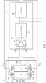
- FIG. 1 shows a block diagram of a MEMS accelerometer 1, here of uniaxial type, comprising a microstructure 2 and a control unit 3, mutually coupled.
- a MEMS accelerometer here of uniaxial type, comprising a microstructure 2 and a control unit 3, mutually coupled.
- the invention is not limited to the sole uniaxial accelerometers.
- the microstructure 2 comprises a supporting body 4 and a movable mass 5, here illustrated only schematically.
- the movable mass 5 is coupled to the supporting body 4 so as to be able to oscillate along a sensing axis and comprises a sensing structure 7 and a driving structure 10, electrically insulated from each other and mechanically coupled to each other.
- the sensing structure 7 and the driving structure 10 are rigidly coupled to each other.
- the movable mass 5 is capacitively coupled to the supporting body 4 in a differential manner. More precisely, the supporting body 4 is provided with a first sensing terminal 11a, a second sensing terminal 11b, a first driving terminal 12a and a second driving terminal 12b.
- the sensing structure 7 is capacitively coupled to the first sensing terminal 11a and the second sensing terminal 11b. Furthermore, the sensing structure 7 is provided with a reading terminal 7a, receiving a reading signal S R , for example a square-wave signal with a frequency between 10 kHz and 1 MHz.
- a first sensing capacitance C S1 and a second sensing capacitance C S2 are present between the sensing structure 7 and the first sensing terminal 11a and between the sensing structure 7 and the second sensing terminal 11b.
- the first sensing capacitance C S1 and the second sensing capacitance C S2 vary in a differential manner as a function of the movements of the movable mass 5.
- the first sensing capacitance C S1 increases (decreases) by an amount and the second sensing capacitance C S2 decreases (increases) by the same amount.
- the driving structure 10 is coupled in a differential manner to the first driving terminal 12a and the second driving terminal 12b. Furthermore, the driving structure 10 is provided with a biasing terminal 10a, receiving a direct biasing voltage V D .
- a first driving capacitance C D1 and a second driving capacitance C D2 varying in a differential manner as a function of the movements of the movable mass 5, are present between the driving structure 10 and the first driving terminal 12a and the second driving terminal 12b.
- the control unit 3 comprises a charge-to-voltage converter 15, a controller 17 and a driver stage 18, which, with the microstructure 2, form a force feedback loop configured to maintain the movable mass 5 in a rest position.
- the charge-to-voltage converter 15 is for example a fully-differential operational amplifier in charge integrator configuration and has a first reading input 15a and a second reading input 15b respectively coupled to the first sensing terminal 11a and the second sensing terminal 11b of the microstructure 2 to receive charge packets in response to switchings of the reading signal S R .
- the charge-to-voltage converter 15 converts the received charge packets into a sensing signal Ss which is supplied to the controller 17.
- the sensing signal Ss is indicative of the position of the movable mass 5 with respect to the rest position.
- the controller 17 determines a control signal S C (normally a control voltage) indicative of the feedback forces to be applied to the movable mass 5 to bring the same movable mass 5 back to a rest position.
- the amplitude of the control signal S C which is made available on the output of the accelerometer 1, is also indicative of the acceleration acting on the accelerometer 1.
- the driver stage 18 converts the control signal S C into a first feedback voltage V FB1 and into a second feedback voltage V FB2 which are applied respectively to the first driving terminal 12a and the second driving terminal 12b to bring the movable mass 5 back to the rest position.
- the movable mass 5 allows to remove the constraints between the signals which are applied for reading and for cancelling the displacements from the rest position.
- the movable mass 5 is a single rigid body, but the driving structure 10 of the movable mass 5 is electrically insulated from the sensing structure 7.
- This measure allows in particular the reading signal S R and the feedback voltages V FB1 , V FB2 (which determine the feedback forces applied to the movable mass 5) to be selected in an independent manner according to the design preferences.
- the amplitude of the reading signal S R may be selected to obtain a high sensitivity, which leads to correspondingly high average values.
- the direct voltage of the driving structure may be selected in an independent manner and, in particular, may be maintained at a value such as to limit consumptions, especially those linked to the charge pump circuits to generate the variable components of the feedback voltages V FB1 , V FB2 even at high frequency. Overall consumptions may be drastically reduced, from the order of milliamperes to the order of hundreds of microamperes.
- the insulation of the sensing structure 7 from the driving structure therefore allows greater freedom of design and sensitivity and consumptions to be defined separately and without conflicting aspects.
- the amplitude of the reading signal S R may be chosen to obtain a desired sensitivity, without this affecting the level of the feedback voltages V FB1 , V FB2 and therefore consumptions.
- the direct voltage of the driving structure 10 is in fact not bound to the average value of the reading signal S R , thanks to the electrical insulation from the sensing structure 7, and may be chosen to obtain the desired feedback forces with the least energy expenditure. For example, it is possible to supply a high biasing voltage (that is static, therefore with low consumptions) and apply low, rapidly variable, feedback voltages V FB1 , V FB2 to the driving terminals 12a, 12b.
- the insulation between the sensing structure 7 and the driving structure 10 of the movable mass 5 also allows to remove spurious contributions linked to the reading signal S R from the transfer function between the driving quantities and the forces applied to the movable mass.
- a further advantage is that the spurious effect of the sensing signal on the driving chain is removed, again due to the insulation described.
- the forces applied to the driving structure 10 depend exclusively on the action of the feedback loop and are not influenced by the square-wave reading signal.
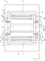
- Figures 2 and 3 show the microstructure 2 according to an embodiment of the invention in a Cartesian reference system XYZ comprising a first axis X, a second axis Y and a third axis Z.
- the microstructure 2 is formed by using MEMS technology, through micromachining techniques, starting from a body of semiconductor material, for example silicon.
- the supporting body 4 comprises a substrate 20 of semiconductor material, for example monocrystalline silicon, an insulating layer 21 extending on the substrate 20, and a supporting frame 22.
- the insulating layer 21 covers the substrate 20 and may include a single dielectric layer, for example silicon oxide, or a multilayer, for example a silicon oxide layer and a silicon nitride layer.
- the supporting frame 22 for example of polycrystalline silicon, is fixed to the insulating layer 21 through conductive contact pads 23 and dielectric anchoring regions 24.
- the supporting frame 22 and the insulating layer 21 laterally and downwardly delimit a cavity 25 where the movable mass 5 is accommodated, suspended at a distance from the insulating layer 21.
- the sensing structure 7 of the movable mass 5 is coupled through flexures 27 to sensing anchors 28.
- the sensing anchors 28 are defined by respective portions of the supporting frame 22 insulated from the remaining portions and are connected, in a manner not illustrated for the sake of simplicity, to the reading terminal 7a.
- the driving structure 10 of the movable mass 5 is coupled through flexures 30 to driving anchors 31.
- the sensing anchors 28 and the driving anchors 31 are defined by respective portions of the supporting frame 22 insulated from the remaining portions and are connected, in a manner not illustrated for the sake of simplicity, to the biasing terminal 10a.
- the flexures 27, 30 are configured so as to allow the movable mass 5 to oscillate along the sensing axis, here parallel to the axis X, with respect to a rest position.
- the electrical connection of the sensing anchors 28 to the reading terminal 7a and of the driving anchors 31 to the biasing terminal 10a may be obtained by buried connection lines (not shown) running on the insulating layer 21.
- the movable mass 5 also comprises a mechanical coupling structure 34, of dielectric material, which rigidly connects the sensing structure 7 and the driving structure 10 to each other, so as to form a single rigid body.
- the sensing structure 7 and the driving structure 10 are mutually spaced and are not in direct contact with each other.
- the sensing structure 7 and the driving structure 10 are separated by a gap 36 and rigidly coupled to each other by the mechanical coupling structure 34, which is placed in the gap 36.
- the sensing structure 7 and the driving structure 10 are therefore electrically insulated from each other.
- the sensing structure 7 and the driving structure 10 have respective mechanical coupling portions 7b, 10b and respective capacitive coupling portions 7c, 10c.
- the capacitive coupling portions 7c, 10c have a first thickness T 1 , equal to the thickness of the supporting frame 22, while the mechanical coupling portions 7b, 10b have a second thickness T 2 smaller than the first thickness T 1 .
- the second thickness T 2 is equal for the mechanical coupling portions 7b, 10b and lower than half of the first thickness T 1 .
- the mechanical coupling portion 10b of the driving structure 10 is superimposed on the mechanical coupling portion 7b of the sensing structure 7 in the direction of the axis Z.
- the mechanical coupling structure 34 rigidly connects the mechanical coupling portion 7b of the sensing structure 7 and the mechanical coupling portion 10b of the driving structure 10 to each other across the gap 36.
- the mechanical coupling structure 34 comprises inner regions 34a and coating regions 34b, which may be of materials selectively etchable by different chemical species.
- the inner regions 34a may be of silicon oxide and the coating regions 34b may be of silicon nitride.
- the inner regions 34a are formed on the mechanical coupling portion 7b of the sensing structure 7.
- the coating regions 34b conformally cover the inner regions 34a and are in contact with the mechanical coupling portion 10b of the driving structure 10. Spaces free from the coating region 34b between inner regions 34a may be occupied by indentations of the mechanical coupling portion 10b.
- the capacitive coupling portions 7c, 10c have respective through openings 38, 40 which extend in the direction of the axis Z throughout the first thickness T 1 and have in plan-view a rectangular shape.
- the openings 38, 40 are delimited by respective flat walls 50, 52 perpendicular to the same sensing axis (i.e. parallel to the coordinate plane YZ).
- the microstructure 2 comprises a first fixed sensing electrode 53a, a second fixed sensing electrode 53b, a first fixed driving electrode 55a and a second fixed driving electrode 55b, all rigidly connected to the supporting body 4.
- the first fixed sensing electrode 53a and the second fixed sensing electrode 53b are defined by flat plates of semiconductor material, for example polycrystalline silicon, which extend perpendicular to the sensing axis (parallel to the coordinate plane YZ).
- the first fixed sensing electrode 53a and the second fixed sensing electrode 53b are accommodated inside the opening 38 of the capacitive coupling portion 7a of the sensing structure 7 and face respective flat walls 50 delimiting the opening 38.
- Conductive lines 56a, 56b running on the dielectric layer 21 connect the first fixed sensing electrode 53a and the second fixed sensing electrode 53b to the first sensing terminal 11a and the second sensing terminal 11b, respectively.
- the sensing structure 7 is thus capacitively coupled to the first sensing terminal 11a and the second sensing terminal 11b with the first sensing capacitance C S1 and with the second sensing capacitance C S2 varying in a differential manner when the movable mass 5 oscillates along the sensing axis.
- the first fixed driving electrode 55a and the second fixed driving electrode 55b are defined by flat plates of semiconductor material, for example polycrystalline silicon, which extend perpendicular to the sensing axis (parallel to the coordinate plane YZ).
- the first fixed driving electrode 55a and the second fixed driving electrode 55b are accommodated inside the opening 40 of the capacitive coupling portion 10c of the driving structure 10 and face respective flat walls 52 of the opening 40.
- Conductive lines 58a, 58b running on the dielectric layer 21 connect the first fixed driving electrode 55a and the second fixed driving electrode 55b to the first driving terminal 12a and the second driving terminal 12b, respectively.
- the driving structure 10 is thus capacitively coupled to the first driving terminal 12a and the second driving terminal 12b with the first driving capacitance C D1 and with the second driving capacitance C D2 varying in a differential manner when the movable mass 5 oscillates along the sensing axis.
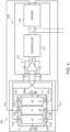
- a microelectromechanical accelerometer in accordance with a different embodiment of the present invention is indicated by 100 and comprises a microstructure 102 and a control unit 103.
- the microstructure 102 comprises a supporting body 104 and a movable mass 105, here illustrated only schematically.
- the movable mass 105 is coupled to the supporting body 104 so as to be able to oscillate along a sensing axis and comprises a first sensing mass 107, a second sensing mass 108, which form a sensing structure, and a driving structure 110.
- the first sensing mass 107, the second sensing mass 108 and the driving structure 110 are electrically insulated from each other and are all mechanically coupled, in particular rigidly coupled, to each other.
- the movable mass 105 is capacitively coupled to the supporting body 104 in a differential manner. More precisely, the supporting body 104 is provided with first sensing terminals 111a, second sensing terminals 111b, a first driving terminal 112a and a second driving terminal 112b.
- the first sensing mass 107 and the second sensing mass 108 are each capacitively coupled to a respective first sensing terminal 111a and a respective second sensing terminal 111b. Furthermore, the first sensing mass 107 and the second sensing mass 108 are respectively provided with a first reading terminal 107a, receiving a first reading signal S R1 , and a second reading terminal 108a, receiving a second reading signal S R2 .
- the first reading signal S R1 and the second reading signal S R2 are for example square-wave signals with a frequency between 10 khz and 1 Mhz and are phase-shifted by 180° with respect to each other.
- first sensing capacitances C S1 and second sensing capacitances Cs 2 varying in a differential manner as a function of the movements of the movable mass 105.
- the first sensing capacitances C S1 (second sensing capacitances C S2 ) vary from each other concordantly with and discordantly from the respective second sensing capacitances C S2 (first sensing capacitances Csi) .
- the first sensing capacitances C S1 increase (decrease) by a same amount and the second sensing capacitances C S2 decrease (increase) by the same amount.
- the driving structure 110 is coupled in a differential manner to the first driving terminal 112a and the second driving terminal 112b. Furthermore, the driving structure 110 is provided with a biasing terminal 110a, receiving a direct biasing voltage V D .
- a first driving capacitance C D1 and a second driving capacitance C D2 varying in a differential manner as a function the movements of the movable mass 105, are present between the driving structure 110 and the first driving terminal 112a and the second driving terminal 112b.
- the first driving capacitance C D1 and a second driving capacitance C D2 vary from each other discordantly. Due to a movement of the movable mass 105 along the sensing axis, the first driving capacitance C D1 increases (decreases) by an amount and the second driving capacitance C D2 decreases (increases) by the same amount.
- the control unit 103 comprises a charge-to-voltage converter 115, a controller 117 and a driver stage 118 which, with the microstructure 102, form a force feedback loop configured to maintain the movable mass 105 in a rest position, substantially as already described.
- the charge-to-voltage converter 115 is for example a fully-differential operational amplifier in charge integrator configuration and is coupled to the microstructure 102 to receive charge packets in response to switchings of the reading signals S R1 , S R2 .
- the charge-to-voltage converter 115 converts the received charge packets into a sensing signal Ss which is supplied to the controller 117.
- the sensing signal Ss is indicative of the position of the movable mass 105 with respect to the rest position.
- the first sensing mass 107 and the second sensing mass 108 each have respective first sensing terminals 111a and second sensing terminals one coupled to a first reading input 115a and the other to a second reading input 115b of the charge-to-voltage converter 115. Furthermore, of the first sensing terminals 111a and the second sensing terminals 111b, one is coupled to the first reading input 115a and the other is coupled to the second reading input 115b.
- the first sensing terminal 111a of the first sensing mass 107 and the second sensing terminal 111b of the second sensing mass 108 are coupled to the first reading input 115a, while the second sensing terminal 111b of the first sensing mass 107 and the first sensing terminal 111a of the second sensing mass 108 are coupled to the second reading input 115b.
- the movable mass 105 in addition to removing the constraints between the signals which are applied for reading and for canceling the displacements from the rest position as already described, enables correct continuous-time operation, which is difficult and complex to implement with the structure of the known accelerometers and would instead be advantageous for a better sensitivity with the same consumption with respect to the discrete-time operation.
- the reading of the accelerometer is based on capacitive coupling variable in a differential manner, modulation through the reading signals produces a common-mode component due to the capacitance at rest which predominates, but is not useful for the purposes of sensing and causes consumptions in particular by the charge-to-voltage converter.
- the compensation capacitances are integrated in the (ASIC, Application Specific Integrated Circuit) chip of the charge-to-voltage converter and receive compensation signals equal to the reading signal, but phase-shifted by 180°. Since the compensation capacitances and the movable mass, with the associated sensing capacitances, cannot be formed by using the same technology, mismatches may easily occur which, in continuous-time operation, worsen the noise and penalize the performances.
- ASIC Application Specific Integrated Circuit
- Another known solution consists in forming a microstructure with two identical movable masses, electrically and mechanically decoupled.
- the two movable masses have sensing terminals connected to the charge-to-voltage converter so as to cancel the common mode and amplify the differential contributions and receive respective reading signals mutually phase-shifted by 180°.
- the matching between the capacitances is much more accurate, but the control stage tends to cancel the overall displacement of the two movable masses and not the displacement of each of the two separately.
- the charge-to-voltage converter receives the sum of the charge contributions due to the displacements of the two movable masses and is not able to distinguish the origin.
- the masses may find themselves in oscillation with even wide displacements with respect to the respective rest positions, with results that may range from a lower linearity than expected up to unreliable readings (for example, if an acceleration triggers phase-opposition oscillations of the movable masses, the accelerometer output may be zero).
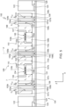
- Figures 5 and 6 show the microstructure 102 according to an embodiment of the invention in a Cartesian reference system XYZ comprising a first axis X, a second axis Y and a third axis Z.
- the supporting body 104 comprises a substrate 120 of semiconductor material, for example monocrystalline silicon, an insulating layer 121, extending on the substrate 120, and a supporting frame 122.
- the insulating layer 121 covers the substrate 120 and may include a single dielectric layer, for example silicon oxide, or a multilayer, for example a silicon oxide layer and a silicon nitride layer.
- the supporting frame 122 for example of polycrystalline silicon, is fixed to the insulating layer 121 through conductive contact pads 123 and dielectric anchoring regions 124.
- the supporting frame 122 and the insulating layer 121 laterally and downwardly delimit a cavity 125 where the movable mass 105 is accommodated, suspended at a distance from the insulating layer 121.
- first sensing mass 107 and the second sensing mass 108 of the movable mass 105 are coupled through flexures 127 to sensing anchors 128.
- the sensing anchors 128 are defined by respective portions of the supporting frame 122 insulated from the remaining portions and are connected, in a manner not illustrated for the sake of simplicity, to the reading terminal 107a (for the first sensing mass 107) and to the second reading terminal 108a (for the second sensing mass 108).
- the driving structure 110 of the movable mass 105 is coupled through flexures 130 to driving anchors 131.
- the sensing anchors 128 and the driving anchors 131 are defined by respective portions of the supporting frame 122 insulated from the remaining portions and are connected, in a manner not illustrated for the sake of simplicity, to the biasing terminal 110a.
- the flexures 127, 130 are configured so as to allow the movable mass 105 to oscillate along the sensing axis, here parallel to the axis X, with respect to a rest position.
- the movable mass 105 also comprises mechanical coupling structures 134, 135 of dielectric material, which rigidly connect the first sensing mass 107, the second sensing mass 108 and the driving structure 110 to each other, so as to form a single rigid body specular symmetrical with respect to a median plane P perpendicular to the sensing axis (and therefore to the axis X).
- the first sensing mass 107 and the second sensing mass 108 are arranged in a specular symmetrical manner on opposite sides of the driving structure 110 with respect to the median plane P of the movable mass 105.
- the driving structure 110 is itself specular symmetrical with respect to the median plane P.
- the first sensing mass 107, the second sensing mass 108 and the driving structure 110 are mutually spaced and are not in direct contact with each other.
- the first sensing mass 107 and the driving structure 110 are separated by a gap 136 and are rigidly coupled to each other by the mechanical coupling structure 134, which is placed in the gap 136.
- the second sensing mass 108 and the driving structure 110 are separated by a gap 137 and are rigidly coupled to each other by the mechanical coupling structure 135, which is placed in the gap 137.
- the first sensing mass 107, the second sensing mass 108 and the driving structure 110 are thus electrically insulated from each other.
- the first sensing mass 107, the second sensing mass 108 and the driving structure 110 have respective mechanical coupling portions 107b, 108b, 110b and respective capacitive coupling portions 107c, 108c, 110c.
- the capacitive coupling portions 107c, 108c, 110c have a first thickness T 1 , equal to the thickness of the supporting frame 122, while the mechanical coupling portions 107b, 108b, 110b have a second thickness T 2 smaller than the first thickness T 1 .
- the second thickness T 2 is equal for the mechanical coupling portions 107b, 108b, 110b and lower than half of the first thickness T 1 .
- the driving structure 110 has two mechanical coupling portions 110b which extend symmetrically in opposite directions with respect to the median plane P. In the direction of the axis Z, the mechanical coupling portions 110b of the driving structure 110 are superimposed one on the mechanical coupling portion 107b of the first sensing mass 107 and the other on the mechanical coupling portion 108b of the second sensing mass 108.
- the mechanical coupling structure 134 rigidly connects the mechanical coupling portion 107b of the first sensing mass 107 to the respective mechanical coupling portion 110b of the driving structure 110 across the gap 136.
- the mechanical coupling structure 135 rigidly connects the mechanical coupling portion 108b of the second sensing mass 108 to the respective mechanical coupling portion 110b of the driving structure 110 across the gap 137.
- the mechanical coupling structures 134, 135 comprise respective inner regions 134a, 135a and coating regions 134b, 135b of materials selectively etchable by different chemical species.
- the inner regions 134a, 135a are respectively formed on the mechanical coupling portion 107b of the first sensing mass 107.
- the coating regions 134b conformally cover the inner regions 134a and are in contact with the mechanical coupling portion 110b of the driving structure 110. Spaces free from the coating region 134b between inner regions 134a may be occupied by indentations of the mechanical coupling portions 110b.
- the capacitive coupling portions 107c, 108c, 110c have respective through openings 138, 139, 140 which extend in the direction of the axis Z throughout the first thickness T 1 and have in plan a rectangular shape.
- the openings 138, 139, 140 are delimited by respective flat walls 150, 151, 152 perpendicular to the same sensing axis (i.e. parallel to the coordinate plane YZ) .
- the microstructure 102 comprises first fixed sensing electrodes 153a, 154a, second fixed sensing electrodes 153b, 154b, a first fixed driving electrode 155a and a second fixed driving electrode 155b, all rigidly connected to the supporting body 104.
- the fixed sensing electrodes 153a, 154a, 153b, 154b and the fixed driving electrodes 155a, 155b are defined by flat plates of semiconductor material, for example polycrystalline silicon, which extend perpendicular to the sensing axis (parallel to the coordinate plane YZ).
- the first fixed sensing electrode 153a and the second fixed sensing electrode 153b are accommodated inside the opening 138 of the capacitive coupling portion 107c of the first sensing mass 107 and face respective flat walls 150 delimiting the opening 138.
- Conductive lines 156a, 156b running on the dielectric layer 121 connect the first fixed sensing electrode 153a and the second fixed sensing electrode 153b to the first sensing terminal 111a and the second sensing terminal 111b of the first sensing mass 107, respectively.
- the first sensing mass 107 is thus capacitively coupled to the first sensing terminal 111a and the second sensing terminal 111b with the first sensing capacitance C S1 and with the second sensing capacitance C S2 varying in a differential manner when the movable mass 105 oscillates along the sensing axis.
- the first fixed sensing electrode 154a and the second fixed sensing electrode 154b are accommodated inside the opening 139 of the capacitive coupling portion 108c of the second sensing mass 108 and face respective flat walls 151 delimiting the opening 139.
- Conductive lines 156a, 156b running on the dielectric layer 121 connect the first fixed sensing electrode 154a and the second fixed sensing electrode 154b to the first sensing terminal 111a and the second sensing terminal 111b of the second sensing mass 108, respectively.
- the second sensing mass 108 is thus capacitively coupled to the first sensing terminal 111a and the second sensing terminal 111b with the first sensing capacitance C S1 and with the second sensing capacitance C S2 varying in a differential manner when the movable mass 105 oscillates along the sensing axis.
- the first fixed driving electrode 155a and the second fixed driving electrode 155b are accommodated inside the opening 140 of the capacitive coupling portion 110c of the driving structure 110 and face respective flat walls 151 of the opening 140.
- Conductive lines 158a, 158b running on the dielectric layer 121 connect the first fixed driving electrode 155a and the second fixed driving electrode 155b to the first driving terminal 112a and the second driving terminal 112b, respectively.
- the driving structure 110 is thus capacitively coupled to the first driving terminal 112a and the second driving terminal 112b with the first driving capacitance C D1 and with the second driving capacitance C D2 varying in a differential manner when the movable mass 105 oscillates along the sensing axis.
Landscapes
- Physics & Mathematics (AREA)
- General Physics & Mathematics (AREA)
- Engineering & Computer Science (AREA)
- Computer Hardware Design (AREA)
- Microelectronics & Electronic Packaging (AREA)
- Pressure Sensors (AREA)
Abstract
Description
- The present invention relates to a microelectromechanical accelerometer with force feedback loop.
- As is known, there are different types of microelectromechanical accelerometers which differ in terms of structure and operating modes. Among these, in particular, the accelerometers with force feedback loop are advantageous due to their high linearity.
- Typically, an accelerometer with force feedback loop comprises a movable mass, a charge-to-voltage converter, a feedback stage, and a driver stage.
- The movable mass, of semiconductor material, is capacitively coupled to sensing electrodes and to driving electrodes with a variable sensing capacitance and driving capacitance, which are determined by the position of the movable mass with respect to a rest position. The charge-to-voltage converter is coupled to the sensing electrodes and transduces the displacements of the movable mass due to accelerations into electrical quantities (normally voltages). More precisely, the instant value of the sensing capacitance may be read by applying a reading signal, generally a square-wave voltage, to the movable mass. The reading signal moves charge packets which depend on the sensing capacitance and therefore on the position of the movable mass. The charge-to-voltage converter receives charge packets and converts them into sensing signals (voltages) . On the basis of the sensing signals, the feedback stage determines feedback forces to be applied to bring the movable mass back to the rest position when the movable mass tends to displace due to accelerations. The driver stage applies the feedback forces to the movable mass by supplying feedback voltages to the driving electrodes. The intensity of the control action exerted by the feedback stage to maintain the movable mass in the rest position is indicative of the accelerations acting on the same movable mass.
- However, the structure of known accelerometers has limitations which do not allow parameters of extreme interest for the market to be developed simultaneously. For various reasons, on the one hand performances, in particular accuracy and sensitivity, and on the other consumptions have conflicting aspects.
- For example, an effective manner to increase the sensitivity of devices is to increase the amplitude of the reading signals. Since, for structural reasons, it is generally much simpler and preferred to use unipolar reading signals, generally positive voltages, an increase in amplitude translates into an increase in the average voltage applied to the movable mass. On the other hand, the request for reducing consumptions leads in the exact opposite direction. In fact, the feedback forces applied to the movable mass by the feedback stage through the driver stage depend on the difference between the common mode of the feedback voltages and the average value of the voltage on the movable mass, which coincides with the average value of the reading signal. Therefore, there is an interest in reducing the average value of the reading signal which conflicts with the interest in increasing the same value to improve sensitivity.
- Another limitation is given by the fact that the noise of the driver stage influences the overall performances in terms of noise, due to the fact that the movable mass is conductive. To overcome this drawback, one solution is to increase the current of the driver stage. The current of the driver stage, which is variable with a wider bandwidth than the feedback loop bandwidth to be able to apply the suitable feedback forces, is generally supplied thanks to charge pump circuits (especially in the case of large full scale devices). While the static consumption of the charge pump circuits is not critical, the dynamic consumption is very high and heavily affects the overall consumption of the devices.
- Another factor which affects the performances of the devices is due to the fact that the transfer function between the driving quantities and the forces applied to the movable mass is not ideal but contains spurious contributions which depend on the reading frequency of the reading signal applied to the movable mass. Unwanted signals at the reading frequency, for example due to noise, are in practice demodulated and brought back to the base band, superimposing on the useful signal.
-
US 2018/031601 A1 discloses a microelectromechanical accelerometer comprising a control unit and a microstructure, provided with sensing terminals and driving terminals distinct from the sensing terminals and including a supporting body and a movable mass, coupled to the supporting body so as to be able to oscillate according to a sensing axis with respect to a rest position. The movable mass comprises a sensing structure coupled to the sensing terminals through a sensing capacitive coupling variable as a function of displacements of the movable mass from the rest position; and a driving structure coupled to the driving terminals through a driving capacitive coupling variable as a function of displacements of the movable mass from the rest position. - Other examples of known microelectromechanical accelerometers are disclosed in
US 2008/190198 , inEP 1 832 841 A1US 2011/197675 A1 . - It is therefore an aim of the present invention to provide a microelectromechanical accelerometer which allows the limitations described to be overcome or at least mitigated.
- According to the present invention, a microelectromechanical accelerometer is provided as defined in
claim 1. - For a better understanding of the present invention, preferred embodiments are presented, by way of non-limiting example, with reference to the attached drawings, wherein:
-
Figure 1 is a simplified block diagram of a microelectromechanical accelerometer according to an embodiment of the present invention; -
Figure 2 is a cross-section through a component of the accelerometer ofFigure 1 ; -
Figure 3 is a top-plan view of the component ofFigure 2 ; -
Figure 4 is a simplified block diagram of a microelectromechanical accelerometer according to a different embodiment of the present invention; -
Figure 5 is a cross-section through a component of the accelerometer ofFigure 4 ; -
Figure 6 is a top-plan view of the component ofFigure 5 . - The following description refers to the arrangement shown; consequently, expressions such as "above", "below", "top", "bottom", relate to the accompanying Figures and are not to be interpreted in a limiting manner.
-
Figure 1 shows a block diagram of aMEMS accelerometer 1, here of uniaxial type, comprising amicrostructure 2 and acontrol unit 3, mutually coupled. However, it is understood that the invention is not limited to the sole uniaxial accelerometers. - The
microstructure 2 comprises a supportingbody 4 and amovable mass 5, here illustrated only schematically. Themovable mass 5 is coupled to the supportingbody 4 so as to be able to oscillate along a sensing axis and comprises asensing structure 7 and adriving structure 10, electrically insulated from each other and mechanically coupled to each other. In particular, thesensing structure 7 and thedriving structure 10 are rigidly coupled to each other. - The
movable mass 5 is capacitively coupled to the supportingbody 4 in a differential manner. More precisely, the supportingbody 4 is provided with afirst sensing terminal 11a, asecond sensing terminal 11b, afirst driving terminal 12a and asecond driving terminal 12b. - The
sensing structure 7 is capacitively coupled to thefirst sensing terminal 11a and thesecond sensing terminal 11b. Furthermore, thesensing structure 7 is provided with areading terminal 7a, receiving a reading signal SR, for example a square-wave signal with a frequency between 10 kHz and 1 MHz. A first sensing capacitance CS1 and a second sensing capacitance CS2 are present between thesensing structure 7 and thefirst sensing terminal 11a and between thesensing structure 7 and thesecond sensing terminal 11b. The first sensing capacitance CS1 and the second sensing capacitance CS2 vary in a differential manner as a function of the movements of themovable mass 5. In practice, due to a movement of themovable mass 5 along the sensing axis, the first sensing capacitance CS1 increases (decreases) by an amount and the second sensing capacitance CS2 decreases (increases) by the same amount. - Similarly, the
driving structure 10 is coupled in a differential manner to thefirst driving terminal 12a and thesecond driving terminal 12b. Furthermore, thedriving structure 10 is provided with abiasing terminal 10a, receiving a direct biasing voltage VD. A first driving capacitance CD1 and a second driving capacitance CD2, varying in a differential manner as a function of the movements of themovable mass 5, are present between thedriving structure 10 and thefirst driving terminal 12a and thesecond driving terminal 12b. - The
control unit 3 comprises a charge-to-voltage converter 15, acontroller 17 and adriver stage 18, which, with themicrostructure 2, form a force feedback loop configured to maintain themovable mass 5 in a rest position. - The charge-to-
voltage converter 15 is for example a fully-differential operational amplifier in charge integrator configuration and has afirst reading input 15a and asecond reading input 15b respectively coupled to thefirst sensing terminal 11a and thesecond sensing terminal 11b of themicrostructure 2 to receive charge packets in response to switchings of the reading signal SR. The charge-to-voltage converter 15 converts the received charge packets into a sensing signal Ss which is supplied to thecontroller 17. The sensing signal Ss is indicative of the position of themovable mass 5 with respect to the rest position. - On the basis of the sensing signal Ss, the
controller 17 determines a control signal SC (normally a control voltage) indicative of the feedback forces to be applied to themovable mass 5 to bring the samemovable mass 5 back to a rest position. The amplitude of the control signal SC, which is made available on the output of theaccelerometer 1, is also indicative of the acceleration acting on theaccelerometer 1. - The
driver stage 18 converts the control signal SC into a first feedback voltage VFB1 and into a second feedback voltage VFB2 which are applied respectively to thefirst driving terminal 12a and thesecond driving terminal 12b to bring themovable mass 5 back to the rest position. - The
movable mass 5 allows to remove the constraints between the signals which are applied for reading and for cancelling the displacements from the rest position. In fact, themovable mass 5 is a single rigid body, but the drivingstructure 10 of themovable mass 5 is electrically insulated from thesensing structure 7. This measure allows in particular the reading signal SR and the feedback voltages VFB1, VFB2 (which determine the feedback forces applied to the movable mass 5) to be selected in an independent manner according to the design preferences. For example, the amplitude of the reading signal SR may be selected to obtain a high sensitivity, which leads to correspondingly high average values. The direct voltage of the driving structure may be selected in an independent manner and, in particular, may be maintained at a value such as to limit consumptions, especially those linked to the charge pump circuits to generate the variable components of the feedback voltages VFB1, VFB2 even at high frequency. Overall consumptions may be drastically reduced, from the order of milliamperes to the order of hundreds of microamperes. The insulation of thesensing structure 7 from the driving structure therefore allows greater freedom of design and sensitivity and consumptions to be defined separately and without conflicting aspects. - For example, the amplitude of the reading signal SR may be chosen to obtain a desired sensitivity, without this affecting the level of the feedback voltages VFB1, VFB2 and therefore consumptions. The direct voltage of the driving
structure 10 is in fact not bound to the average value of the reading signal SR, thanks to the electrical insulation from thesensing structure 7, and may be chosen to obtain the desired feedback forces with the least energy expenditure. For example, it is possible to supply a high biasing voltage (that is static, therefore with low consumptions) and apply low, rapidly variable, feedback voltages VFB1, VFB2 to thedriving terminals - The insulation between the
sensing structure 7 and the drivingstructure 10 of themovable mass 5 also allows to remove spurious contributions linked to the reading signal SR from the transfer function between the driving quantities and the forces applied to the movable mass. - A further advantage is that the spurious effect of the sensing signal on the driving chain is removed, again due to the insulation described. In practice, the forces applied to the driving
structure 10 depend exclusively on the action of the feedback loop and are not influenced by the square-wave reading signal. -
Figures 2 and3 show themicrostructure 2 according to an embodiment of the invention in a Cartesian reference system XYZ comprising a first axis X, a second axis Y and a third axis Z. - The
microstructure 2 is formed by using MEMS technology, through micromachining techniques, starting from a body of semiconductor material, for example silicon. - The supporting
body 4 comprises asubstrate 20 of semiconductor material, for example monocrystalline silicon, an insulatinglayer 21 extending on thesubstrate 20, and a supportingframe 22. - The insulating
layer 21 covers thesubstrate 20 and may include a single dielectric layer, for example silicon oxide, or a multilayer, for example a silicon oxide layer and a silicon nitride layer. - The supporting
frame 22, for example of polycrystalline silicon, is fixed to the insulatinglayer 21 throughconductive contact pads 23 anddielectric anchoring regions 24. The supportingframe 22 and the insulatinglayer 21 laterally and downwardly delimit acavity 25 where themovable mass 5 is accommodated, suspended at a distance from the insulatinglayer 21. - In more detail, the
sensing structure 7 of themovable mass 5 is coupled throughflexures 27 to sensing anchors 28. The sensing anchors 28 are defined by respective portions of the supportingframe 22 insulated from the remaining portions and are connected, in a manner not illustrated for the sake of simplicity, to the reading terminal 7a. - The driving
structure 10 of themovable mass 5 is coupled throughflexures 30 to driving anchors 31. The sensing anchors 28 and the driving anchors 31 are defined by respective portions of the supportingframe 22 insulated from the remaining portions and are connected, in a manner not illustrated for the sake of simplicity, to the biasing terminal 10a. - The
flexures movable mass 5 to oscillate along the sensing axis, here parallel to the axis X, with respect to a rest position. - The electrical connection of the sensing anchors 28 to the reading terminal 7a and of the driving anchors 31 to the biasing terminal 10a may be obtained by buried connection lines (not shown) running on the insulating
layer 21. - The
movable mass 5 also comprises amechanical coupling structure 34, of dielectric material, which rigidly connects thesensing structure 7 and the drivingstructure 10 to each other, so as to form a single rigid body. Thesensing structure 7 and the drivingstructure 10 are mutually spaced and are not in direct contact with each other. In particular, thesensing structure 7 and the drivingstructure 10 are separated by agap 36 and rigidly coupled to each other by themechanical coupling structure 34, which is placed in thegap 36. Thesensing structure 7 and the drivingstructure 10 are therefore electrically insulated from each other. - In more detail, the
sensing structure 7 and the drivingstructure 10 have respectivemechanical coupling portions capacitive coupling portions capacitive coupling portions frame 22, while themechanical coupling portions Figures 2 and3 , the second thickness T2 is equal for themechanical coupling portions - The
mechanical coupling portion 10b of the drivingstructure 10 is superimposed on themechanical coupling portion 7b of thesensing structure 7 in the direction of the axis Z. Themechanical coupling structure 34 rigidly connects themechanical coupling portion 7b of thesensing structure 7 and themechanical coupling portion 10b of the drivingstructure 10 to each other across thegap 36. - In one embodiment, the
mechanical coupling structure 34 comprisesinner regions 34a andcoating regions 34b, which may be of materials selectively etchable by different chemical species. For example, theinner regions 34a may be of silicon oxide and thecoating regions 34b may be of silicon nitride. Theinner regions 34a are formed on themechanical coupling portion 7b of thesensing structure 7. Thecoating regions 34b conformally cover theinner regions 34a and are in contact with themechanical coupling portion 10b of the drivingstructure 10. Spaces free from thecoating region 34b betweeninner regions 34a may be occupied by indentations of themechanical coupling portion 10b. - The
capacitive coupling portions openings openings flat walls - The
microstructure 2 comprises a firstfixed sensing electrode 53a, a secondfixed sensing electrode 53b, a firstfixed driving electrode 55a and a second fixed drivingelectrode 55b, all rigidly connected to the supportingbody 4. - The first
fixed sensing electrode 53a and the secondfixed sensing electrode 53b are defined by flat plates of semiconductor material, for example polycrystalline silicon, which extend perpendicular to the sensing axis (parallel to the coordinate plane YZ). The firstfixed sensing electrode 53a and the secondfixed sensing electrode 53b are accommodated inside theopening 38 of thecapacitive coupling portion 7a of thesensing structure 7 and face respectiveflat walls 50 delimiting theopening 38.Conductive lines dielectric layer 21 connect the firstfixed sensing electrode 53a and the secondfixed sensing electrode 53b to thefirst sensing terminal 11a and thesecond sensing terminal 11b, respectively. Thesensing structure 7 is thus capacitively coupled to thefirst sensing terminal 11a and thesecond sensing terminal 11b with the first sensing capacitance CS1 and with the second sensing capacitance CS2 varying in a differential manner when themovable mass 5 oscillates along the sensing axis. - The first
fixed driving electrode 55a and the second fixed drivingelectrode 55b are defined by flat plates of semiconductor material, for example polycrystalline silicon, which extend perpendicular to the sensing axis (parallel to the coordinate plane YZ). The firstfixed driving electrode 55a and the second fixed drivingelectrode 55b are accommodated inside theopening 40 of thecapacitive coupling portion 10c of the drivingstructure 10 and face respectiveflat walls 52 of theopening 40.Conductive lines dielectric layer 21 connect the firstfixed driving electrode 55a and the second fixed drivingelectrode 55b to thefirst driving terminal 12a and thesecond driving terminal 12b, respectively. The drivingstructure 10 is thus capacitively coupled to thefirst driving terminal 12a and thesecond driving terminal 12b with the first driving capacitance CD1 and with the second driving capacitance CD2 varying in a differential manner when themovable mass 5 oscillates along the sensing axis. - With reference to
Figures 4-6 , a microelectromechanical accelerometer in accordance with a different embodiment of the present invention is indicated by 100 and comprises amicrostructure 102 and acontrol unit 103. - The
microstructure 102 comprises a supportingbody 104 and amovable mass 105, here illustrated only schematically. Themovable mass 105 is coupled to the supportingbody 104 so as to be able to oscillate along a sensing axis and comprises afirst sensing mass 107, asecond sensing mass 108, which form a sensing structure, and a drivingstructure 110. Thefirst sensing mass 107, thesecond sensing mass 108 and the drivingstructure 110 are electrically insulated from each other and are all mechanically coupled, in particular rigidly coupled, to each other. - The
movable mass 105 is capacitively coupled to the supportingbody 104 in a differential manner. More precisely, the supportingbody 104 is provided withfirst sensing terminals 111a,second sensing terminals 111b, afirst driving terminal 112a and asecond driving terminal 112b. - The
first sensing mass 107 and thesecond sensing mass 108 are each capacitively coupled to a respectivefirst sensing terminal 111a and a respectivesecond sensing terminal 111b. Furthermore, thefirst sensing mass 107 and thesecond sensing mass 108 are respectively provided with afirst reading terminal 107a, receiving a first reading signal SR1, and asecond reading terminal 108a, receiving a second reading signal SR2. The first reading signal SR1 and the second reading signal SR2 are for example square-wave signals with a frequency between 10 khz and 1 Mhz and are phase-shifted by 180° with respect to each other. Between each of thefirst sensing mass 107 and thesecond sensing mass 108 and the respectivefirst sensing terminals 111a andsecond sensing terminals 111b there are present first sensing capacitances CS1 and second sensing capacitances Cs2, varying in a differential manner as a function of the movements of themovable mass 105. The first sensing capacitances CS1 (second sensing capacitances CS2) vary from each other concordantly with and discordantly from the respective second sensing capacitances CS2 (first sensing capacitances Csi) . Due to a movement of themovable mass 105 along the sensing axis, the first sensing capacitances CS1 increase (decrease) by a same amount and the second sensing capacitances CS2 decrease (increase) by the same amount. - Similarly, the driving
structure 110 is coupled in a differential manner to thefirst driving terminal 112a and thesecond driving terminal 112b. Furthermore, the drivingstructure 110 is provided with a biasing terminal 110a, receiving a direct biasing voltage VD. A first driving capacitance CD1 and a second driving capacitance CD2, varying in a differential manner as a function the movements of themovable mass 105, are present between the drivingstructure 110 and thefirst driving terminal 112a and thesecond driving terminal 112b. The first driving capacitance CD1 and a second driving capacitance CD2 vary from each other discordantly. Due to a movement of themovable mass 105 along the sensing axis, the first driving capacitance CD1 increases (decreases) by an amount and the second driving capacitance CD2 decreases (increases) by the same amount. - The
control unit 103 comprises a charge-to-voltage converter 115, acontroller 117 and adriver stage 118 which, with themicrostructure 102, form a force feedback loop configured to maintain themovable mass 105 in a rest position, substantially as already described. - The charge-to-
voltage converter 115 is for example a fully-differential operational amplifier in charge integrator configuration and is coupled to themicrostructure 102 to receive charge packets in response to switchings of the reading signals SR1, SR2. The charge-to-voltage converter 115 converts the received charge packets into a sensing signal Ss which is supplied to thecontroller 117. The sensing signal Ss is indicative of the position of themovable mass 105 with respect to the rest position. - In more detail, the
first sensing mass 107 and thesecond sensing mass 108 each have respectivefirst sensing terminals 111a and second sensing terminals one coupled to afirst reading input 115a and the other to asecond reading input 115b of the charge-to-voltage converter 115. Furthermore, of thefirst sensing terminals 111a and thesecond sensing terminals 111b, one is coupled to thefirst reading input 115a and the other is coupled to thesecond reading input 115b. In the embodiment ofFigures 4-6 , for example, thefirst sensing terminal 111a of thefirst sensing mass 107 and thesecond sensing terminal 111b of thesecond sensing mass 108 are coupled to thefirst reading input 115a, while thesecond sensing terminal 111b of thefirst sensing mass 107 and thefirst sensing terminal 111a of thesecond sensing mass 108 are coupled to thesecond reading input 115b. - On the basis of the sensing signal Ss, the
controller 117 determines a control signal SC (usually a control voltage) indicative of feedback forces to be applied to themovable mass 105 to bring the samemovable mass 105 back to a rest position. The amplitude of the control signal SC, which is made available on the output of the accelerometer 101, is also indicative of the acceleration acting on the accelerometer 101. - The
driver stage 118 converts the control signal SC into a first feedback voltage VFB1 and into a second feedback voltage VFB2 which are applied respectively to thefirst driving terminal 112a and thesecond driving terminal 112b to bring themovable mass 105 back to the rest position. - The
movable mass 105, in addition to removing the constraints between the signals which are applied for reading and for canceling the displacements from the rest position as already described, enables correct continuous-time operation, which is difficult and complex to implement with the structure of the known accelerometers and would instead be advantageous for a better sensitivity with the same consumption with respect to the discrete-time operation. Although the reading of the accelerometer is based on capacitive coupling variable in a differential manner, modulation through the reading signals produces a common-mode component due to the capacitance at rest which predominates, but is not useful for the purposes of sensing and causes consumptions in particular by the charge-to-voltage converter. The common-mode component should therefore be compensated and, in continuous-time operation, this may be done in two manners, again including compensation capacitances which are coupled to the inputs of the charge-to-voltage converter and replicate the capacitances between the supporting body and the movable mass in the rest position. - In a first solution, the compensation capacitances are integrated in the (ASIC, Application Specific Integrated Circuit) chip of the charge-to-voltage converter and receive compensation signals equal to the reading signal, but phase-shifted by 180°. Since the compensation capacitances and the movable mass, with the associated sensing capacitances, cannot be formed by using the same technology, mismatches may easily occur which, in continuous-time operation, worsen the noise and penalize the performances.
- Another known solution consists in forming a microstructure with two identical movable masses, electrically and mechanically decoupled. The two movable masses have sensing terminals connected to the charge-to-voltage converter so as to cancel the common mode and amplify the differential contributions and receive respective reading signals mutually phase-shifted by 180°. In this case, the matching between the capacitances is much more accurate, but the control stage tends to cancel the overall displacement of the two movable masses and not the displacement of each of the two separately. In fact, the charge-to-voltage converter receives the sum of the charge contributions due to the displacements of the two movable masses and is not able to distinguish the origin. Despite the action of the control stage, therefore, due to unavoidable imperfections, the masses may find themselves in oscillation with even wide displacements with respect to the respective rest positions, with results that may range from a lower linearity than expected up to unreliable readings (for example, if an acceleration triggers phase-opposition oscillations of the movable masses, the accelerometer output may be zero).
- In the
movable mass 105, on the other hand, thefirst sensing mass 107 and thesecond sensing mass 108 are both rigidly coupled to the drivingstructure 110 and, consequently, also to each other. In addition to the advantage of a very accurate matching between capacitances, the mechanical constraint ensures that thefirst sensing mass 107 and thesecond sensing mass 108 always move in-phase and without relative displacements. Therefore, the overall displacement of themovable mass 105 coincides with the displacements of each of thefirst sensing mass 107 and thesecond sensing mass 108, the action of the force feedback loop is effective and the readings are correct. -
Figures 5 and6 show themicrostructure 102 according to an embodiment of the invention in a Cartesian reference system XYZ comprising a first axis X, a second axis Y and a third axis Z. - The
microstructure 102 is formed in MEMS technology, through micromachining techniques, starting from a body of semiconductor material, for example silicon. - The supporting
body 104 comprises a substrate 120 of semiconductor material, for example monocrystalline silicon, an insulatinglayer 121, extending on the substrate 120, and a supportingframe 122. - The insulating
layer 121 covers the substrate 120 and may include a single dielectric layer, for example silicon oxide, or a multilayer, for example a silicon oxide layer and a silicon nitride layer. - The supporting
frame 122, for example of polycrystalline silicon, is fixed to the insulatinglayer 121 throughconductive contact pads 123 anddielectric anchoring regions 124. The supportingframe 122 and the insulatinglayer 121 laterally and downwardly delimit acavity 125 where themovable mass 105 is accommodated, suspended at a distance from the insulatinglayer 121. - In more detail, the
first sensing mass 107 and thesecond sensing mass 108 of themovable mass 105 are coupled throughflexures 127 to sensing anchors 128. The sensing anchors 128 are defined by respective portions of the supportingframe 122 insulated from the remaining portions and are connected, in a manner not illustrated for the sake of simplicity, to thereading terminal 107a (for the first sensing mass 107) and to thesecond reading terminal 108a (for the second sensing mass 108). - The driving
structure 110 of themovable mass 105 is coupled throughflexures 130 to driving anchors 131. The sensing anchors 128 and the driving anchors 131 are defined by respective portions of the supportingframe 122 insulated from the remaining portions and are connected, in a manner not illustrated for the sake of simplicity, to the biasing terminal 110a. - The
flexures movable mass 105 to oscillate along the sensing axis, here parallel to the axis X, with respect to a rest position. - The
movable mass 105 also comprisesmechanical coupling structures first sensing mass 107, thesecond sensing mass 108 and the drivingstructure 110 to each other, so as to form a single rigid body specular symmetrical with respect to a median plane P perpendicular to the sensing axis (and therefore to the axis X). - In more detail, the
first sensing mass 107 and thesecond sensing mass 108 are arranged in a specular symmetrical manner on opposite sides of the drivingstructure 110 with respect to the median plane P of themovable mass 105. The drivingstructure 110 is itself specular symmetrical with respect to the median plane P. - The
first sensing mass 107, thesecond sensing mass 108 and the drivingstructure 110 are mutually spaced and are not in direct contact with each other. Thefirst sensing mass 107 and the drivingstructure 110 are separated by agap 136 and are rigidly coupled to each other by themechanical coupling structure 134, which is placed in thegap 136. Thesecond sensing mass 108 and the drivingstructure 110 are separated by agap 137 and are rigidly coupled to each other by themechanical coupling structure 135, which is placed in thegap 137. - The
first sensing mass 107, thesecond sensing mass 108 and the drivingstructure 110 are thus electrically insulated from each other. - In more detail, the
first sensing mass 107, thesecond sensing mass 108 and the drivingstructure 110 have respectivemechanical coupling portions capacitive coupling portions capacitive coupling portions frame 122, while themechanical coupling portions Figures 4 and5 , the second thickness T2 is equal for themechanical coupling portions - The driving
structure 110 has twomechanical coupling portions 110b which extend symmetrically in opposite directions with respect to the median plane P. In the direction of the axis Z, themechanical coupling portions 110b of the drivingstructure 110 are superimposed one on themechanical coupling portion 107b of thefirst sensing mass 107 and the other on themechanical coupling portion 108b of thesecond sensing mass 108. Themechanical coupling structure 134 rigidly connects themechanical coupling portion 107b of thefirst sensing mass 107 to the respectivemechanical coupling portion 110b of the drivingstructure 110 across thegap 136. Themechanical coupling structure 135 rigidly connects themechanical coupling portion 108b of thesecond sensing mass 108 to the respectivemechanical coupling portion 110b of the drivingstructure 110 across thegap 137. - In one embodiment, the
mechanical coupling structures inner regions coating regions inner regions mechanical coupling portion 107b of thefirst sensing mass 107. Thecoating regions 134b conformally cover theinner regions 134a and are in contact with themechanical coupling portion 110b of the drivingstructure 110. Spaces free from thecoating region 134b betweeninner regions 134a may be occupied by indentations of themechanical coupling portions 110b. - The
capacitive coupling portions openings openings flat walls - The
microstructure 102 comprises first fixedsensing electrodes fixed sensing electrodes fixed driving electrode 155a and a second fixed drivingelectrode 155b, all rigidly connected to the supportingbody 104. - The fixed
sensing electrodes driving electrodes - The first
fixed sensing electrode 153a and the secondfixed sensing electrode 153b are accommodated inside theopening 138 of thecapacitive coupling portion 107c of thefirst sensing mass 107 and face respectiveflat walls 150 delimiting theopening 138.Conductive lines dielectric layer 121 connect the firstfixed sensing electrode 153a and the secondfixed sensing electrode 153b to thefirst sensing terminal 111a and thesecond sensing terminal 111b of thefirst sensing mass 107, respectively. Thefirst sensing mass 107 is thus capacitively coupled to thefirst sensing terminal 111a and thesecond sensing terminal 111b with the first sensing capacitance CS1 and with the second sensing capacitance CS2 varying in a differential manner when themovable mass 105 oscillates along the sensing axis. - The first
fixed sensing electrode 154a and the secondfixed sensing electrode 154b are accommodated inside theopening 139 of thecapacitive coupling portion 108c of thesecond sensing mass 108 and face respectiveflat walls 151 delimiting theopening 139.Conductive lines dielectric layer 121 connect the firstfixed sensing electrode 154a and the secondfixed sensing electrode 154b to thefirst sensing terminal 111a and thesecond sensing terminal 111b of thesecond sensing mass 108, respectively. Thesecond sensing mass 108 is thus capacitively coupled to thefirst sensing terminal 111a and thesecond sensing terminal 111b with the first sensing capacitance CS1 and with the second sensing capacitance CS2 varying in a differential manner when themovable mass 105 oscillates along the sensing axis. - The first
fixed driving electrode 155a and the second fixed drivingelectrode 155b are accommodated inside theopening 140 of thecapacitive coupling portion 110c of the drivingstructure 110 and face respectiveflat walls 151 of theopening 140.Conductive lines dielectric layer 121 connect the firstfixed driving electrode 155a and the second fixed drivingelectrode 155b to thefirst driving terminal 112a and thesecond driving terminal 112b, respectively. The drivingstructure 110 is thus capacitively coupled to thefirst driving terminal 112a and thesecond driving terminal 112b with the first driving capacitance CD1 and with the second driving capacitance CD2 varying in a differential manner when themovable mass 105 oscillates along the sensing axis. - Finally, it is clear that modifications and variations may be made to the microelectromechanical accelerometer described, without departing from the scope of the present invention, as defined in the attached claims.
- In particular, for the sake of simplicity, reference has been made in the preceding description to uniaxial accelerometers. However, it is understood that the invention may equally be applied to multi-axial accelerometers.
Claims (15)
- A microelectromechanical accelerometer comprising:a microstructure (2; 102), provided with sensing terminals (11a, 11b; 111a, 111b) and driving terminals (12a, 12b; 112a, 112b) distinct from the sensing terminals (11a, 11b; 111a, 111b) and including a supporting body (4; 104) and a movable mass (5; 105), coupled to the supporting body (4; 104) so as to be able to oscillate according to a sensing axis (X) with respect to a rest position; anda control unit (3; 103);wherein the movable mass (5; 105) comprises:a sensing structure (7; 107, 108) coupled to the sensing terminals (11a, 11b; 111a, 111b) through a sensing capacitive coupling (CS1, CS2) variable as a function of displacements of the movable mass (5; 105) from the rest position; anda driving structure (10; 110) coupled to the driving terminals (12a, 12b; 112a, 112b) through a driving capacitive coupling (CD1, CD2) variable as a function of displacements of the movable mass (5; 105) from the rest position;characterized in that the control unit (3; 103) is coupled to the microstructure (2; 102) so as to form a force feedback loop configured to maintain the movable mass (5; 105) in the rest position and in that the sensing structure (7; 107, 108) and the driving structure (10; 110) are electrically insulated from and rigidly coupled to each other.
- The accelerometer according to claim 1, wherein the control unit (3; 103) is coupled to the sensing terminals (11a, 11b; 111a, 111b) and the driving terminals (12a, 12b; 112a, 112b) of the movable mass (5; 105) and is configured to sense displacements of the movable mass (5; 105) from the rest position through the sensing terminals (11a, 11b; 111a, 111b) and to apply feedback forces to the movable mass (5 ; 105) through feedback signals (VFB1, VFB2) supplied to the driving terminals (12a, 12b; 112a, 112b).
- The accelerometer according to claim 2, wherein the control unit (3; 103) comprises:a sensing device (15; 115) coupled to the sensing terminals (11a, 11b; 111a, 111b) of the movable mass (5; 105) and configured to supply a sensing signal (Ss) as a function of the displacements of the movable mass (5; 105) from the rest position; anda control device (17, 18; 117, 118) coupled to the driving terminals (12a, 12b; 112a, 112b) of the movable mass (5; 105) and configured to supply the feedback signals (VFB1, VFB2) as a function of the sensing signal (Ss).
- The accelerometer according to any of the preceding claims, wherein the microstructure (2; 102) comprises:fixed driving electrodes (55a, 55b; 155a, 155b) rigidly connected to the supporting body (4; 104) and coupled to the driving terminals (12a, 12b; 112a, 112b); andfixed sensing electrodes (53a, 53b; 153a, 153b, 154a, 154b) rigidly connected to the supporting body (4; 104) and coupled to the sensing terminals (11a, 11b; 111a, 111b);wherein the driving structure (10; 110) is capacitively coupled to the fixed driving electrodes (55a, 55b; 155a, 155b) through the driving capacitive coupling (CD1, CD2) in a differential manner; andwherein the sensing structure (7; 107, 108) is capacitively coupled to the fixed sensing electrodes (53a, 53b; 153a, 153b, 154a, 154b) through the sensing capacitive coupling (CS1, CS2) in a differential manner.
- The accelerometer according to claim 4, wherein the fixed driving electrodes (55a, 55b; 155a, 155b) are defined by flat semiconductor plates perpendicular to the sensing axis (X), wherein the driving structure (10; 110) has a through opening (40; 140) and wherein the fixed driving electrodes (55a, 55b; 155a, 155b) are accommodated inside the through opening (40; 140) of the driving structure (10; 110) and are capacitively coupled to respective walls (52; 152) of the through opening (40; 140); and
wherein the fixed sensing electrodes (53a, 53b; 153a, 153b, 154a, 154b) are defined by flat semiconductor plates perpendicular to the sensing axis (X), wherein the sensing structure (7; 107, 108) has a through opening (38; 138, 139) and wherein the fixed sensing electrodes (53a, 53b; 153a, 153b, 154a, 154b) are accommodated inside the through opening (38; 138, 139) of the sensing structure (7; 107, 108) and are capacitively coupled to respective walls (50; 150, 151) delimiting the through opening (38; 138, 139) and perpendicular to the sensing axis (X). - The accelerometer according to any of the preceding claims, wherein the sensing structure (107, 108) comprises a first sensing mass (107) and a second sensing mass (108), both rigidly coupled to the driving structure (110) and electrically insulated from the driving structure (110) and from each other.
- The accelerometer according to claim 6, wherein:the sensing terminals (11a, 11b; 111a, 111b) comprise first sensing terminals (111a) and second sensing terminals (111b);the first sensing mass (107) is capacitively coupled to a respective one of the sensing terminals (111a) and a respective one of the second sensing terminals (111b);the second sensing mass (108) is capacitively coupled to a respective one of the first sensing terminals (111a), distinct from the first sensing terminal (111a) of the first sensing mass (107), and to a respective one of the second sensing terminals (111b), distinct from the second sensing terminal (111b) of the first sensing mass (107);the first sensing terminal (111a) of the first sensing mass (107) and the second sensing terminal (111b) of the second sensing mass (108) are coupled to a first reading input (115a) of the control unit (3; 103);the first sensing terminal (111a) of the second sensing mass (108) and the second sensing terminal (111b) of the first sensing mass (107) are coupled to a second reading input (115b) of the control unit (3; 103).
- The accelerometer according to claim 7 depending on claim 4, wherein:the fixed sensing electrodes (153a, 153b, 154a, 154b) comprise first fixed sensing electrodes (153a, 154a) and second fixed sensing electrodes (153b, 154b);the first sensing mass (107) is capacitively coupled to a respective one of the first fixed sensing electrodes (153a) and to a respective one of the second fixed sensing electrodes (153b);the second sensing mass (108) is capacitively coupled to a respective one of the first fixed sensing electrodes (154a), distinct from the first fixed sensing electrode (154a) coupled to the first sensing mass (107), and to a respective one of the second fixed sensing electrodes (153b, 154b), distinct from the second fixed sensing electrode (153b) coupled to the first sensing mass (107).
- The accelerometer according to claim 8, wherein:the first sensing mass (107) and the second sensing mass (108) each have a respective through opening (138, 139);the first fixed sensing electrode (153a) and the second fixed sensing electrode (153b) coupled to the first sensing mass (107) are accommodated inside the through opening (138) of the first sensing mass (107);the first fixed sensing electrode (154a) and the second fixed sensing electrode (154b) coupled to the second sensing mass (108) are accommodated inside the through opening (138) of the second sensing mass (108); andthe first fixed sensing electrodes (153a, 154a) and second fixed sensing electrodes (153b, 154b) are capacitively coupled to respective walls (150, 151) delimiting the through openings (138, 139) and perpendicular to the sensing axis (X) wherein the first fixed sensing electrodes (153a, 154a) and second fixed sensing electrodes (153b, 154b) are respectively accommodated.
- The accelerometer according to claim 8 or 9, wherein:the first fixed sensing electrode (153a) and the second fixed sensing electrode (153b) coupled to the first sensing mass (107) are respectively connected to the first sensing terminal (111a) and to the second sensing terminal (111b) of the first sensing mass (107); andthe first fixed sensing electrode (154a) and the second fixed sensing electrode (154b) coupled to the second sensing mass (108) are respectively connected to the first sensing terminal (111a) and to the second sensing terminal (111b) of the second sensing mass (108).
- The accelerometer according to any of claims 7 to 10, wherein:the sensing capacitive coupling (CS1, CS2) comprises first capacitances (CS1) between the first sensing mass (107) and the respective first sensing terminal (111a) and between the second sensing mass (108) and the respective first sensing terminal (111a) and second capacitances (CS2) between the first sensing mass (107) and the respective second sensing terminal (111b) and between the second sensing mass (108) and the respective second sensing terminal (111b);the first sensing mass (107) and the second sensing mass (108) are coupled to the respective first sensing terminals (111a) and second sensing terminals (111b) so that, due to displacements of the movable mass (5; 105) from the equilibrium position, the first capacitances (CS1) vary concordantly from each other, the second capacitances (CS2) vary concordantly from each other and the first capacitances (CS1) vary discordantly with respect to the second capacitances (CS2).
- The accelerometer according to any of claims 6 to 11, wherein the first sensing mass (107) and the second sensing mass (108) respectively have a first reading terminal (107a) and a second reading terminal (108a) and the control unit (103) is configured to supply a first reading signal (SR1) and a second reading signal (SR2) respectively to the first reading terminal (107a) and to the second reading terminal (108a), the first reading signal (SR1) and the second reading signal (SR2) being phase-shifted by 180° with each other.
- The accelerometer according to any of claims 6 to 12, wherein the sensing structure (107, 108) and the driving structure (110) are specular symmetrical with respect to a median plane (P) of the movable mass (5; 105) perpendicular to the sensing axis (X).
- The accelerometer according to any of the preceding claims, wherein:the sensing structure (7; 107, 108) is separated from the driving structure (10; 110) by at least one gap (36; 136, 137);the sensing structure (7; 107, 108) and the driving structure (10; 110) have respective mechanical coupling portions (7b, 10b; 107b, 108b, 110b);the mechanical coupling portions (7b, 10b; 107b, 108b, 110b) of the driving structure (10; 110) and of the sensing structure (7; 107, 108) are superimposed on each other;the movable mass (5; 105) comprises at least one mechanical coupling structure (34; 134, 135) rigidly connecting the mechanical coupling portions (7b, 10b; 107b, 108b, 110b) of the driving structure (10; 110b) and of the sensing structure (7; 107, 108) to each other across the at least one gap (36; 136, 137).
- The accelerometer according to any of the preceding claims, wherein the control unit (3; 103) is configured to apply reading signals (SR; SR1, SR2) to the sensing structure (7; 107, 108) and a direct voltage (VD) to the driving structure (10; 110), the direct voltage (VD) being independent of an average value of the reading signals (SR; SR1, SR2).
Applications Claiming Priority (1)
| Application Number | Priority Date | Filing Date | Title |
|---|---|---|---|
| IT102023000010326A IT202300010326A1 (en) | 2023-05-22 | 2023-05-22 | MICROELECTROMECHANICAL ACCELEROMETER WITH FORCE FEEDBACK RING |
Publications (2)
| Publication Number | Publication Date |
|---|---|
| EP4467987A1 true EP4467987A1 (en) | 2024-11-27 |
| EP4467987B1 EP4467987B1 (en) | 2026-04-15 |
Family
ID=87280370
Family Applications (1)
| Application Number | Title | Priority Date | Filing Date |
|---|---|---|---|
| EP24176349.9A Active EP4467987B1 (en) | 2023-05-22 | 2024-05-16 | Microelectromechanical accelerometer with force feedback loop |
Country Status (3)
| Country | Link |
|---|---|
| US (1) | US20240391757A1 (en) |
| EP (1) | EP4467987B1 (en) |
| IT (1) | IT202300010326A1 (en) |
Families Citing this family (1)
| Publication number | Priority date | Publication date | Assignee | Title |
|---|---|---|---|---|
| IT202200014548A1 (en) | 2022-07-11 | 2024-01-11 | St Microelectronics Srl | SENSING STRUCTURE FOR A MEMS ACCELEROMETER WITH IMPROVED PERFORMANCE AND RELATED MANUFACTURING PROCEDURE |
Citations (4)
| Publication number | Priority date | Publication date | Assignee | Title |
|---|---|---|---|---|
| EP1832841A1 (en) | 2006-03-10 | 2007-09-12 | STMicroelectronics S.r.l. | Microelectromechanical integrated sensor structure with rotary driving motion |
| US20080190198A1 (en) | 2007-02-13 | 2008-08-14 | Stmicroelectronics S.R.L. | Microelectromechanical gyroscope with suppression of capacitive coupling spurious signals and control method |
| US20110197675A1 (en) | 2010-02-16 | 2011-08-18 | Stmicroelectronics S.R.L. | Microelectromechanical gyroscope with inversion of actuation forces, and method for actuating a microelectromechanical gyroscope |
| US20180031601A1 (en) | 2016-07-27 | 2018-02-01 | Lumedyne Technologies Incorporated | Composite vibratory in-plane accelerometer |
Family Cites Families (2)
| Publication number | Priority date | Publication date | Assignee | Title |
|---|---|---|---|---|
| US8539834B2 (en) * | 2010-02-15 | 2013-09-24 | Stmicroelectronics S.R.L. | Microelectromechanical gyroscope with calibrated synchronization of actuation and method for actuating a microelectromechanical gyroscope |
| IT202200014548A1 (en) * | 2022-07-11 | 2024-01-11 | St Microelectronics Srl | SENSING STRUCTURE FOR A MEMS ACCELEROMETER WITH IMPROVED PERFORMANCE AND RELATED MANUFACTURING PROCEDURE |
-
2023
- 2023-05-22 IT IT102023000010326A patent/IT202300010326A1/en unknown
-
2024
- 2024-05-14 US US18/663,961 patent/US20240391757A1/en active Pending
- 2024-05-16 EP EP24176349.9A patent/EP4467987B1/en active Active
Patent Citations (4)
| Publication number | Priority date | Publication date | Assignee | Title |
|---|---|---|---|---|
| EP1832841A1 (en) | 2006-03-10 | 2007-09-12 | STMicroelectronics S.r.l. | Microelectromechanical integrated sensor structure with rotary driving motion |
| US20080190198A1 (en) | 2007-02-13 | 2008-08-14 | Stmicroelectronics S.R.L. | Microelectromechanical gyroscope with suppression of capacitive coupling spurious signals and control method |
| US20110197675A1 (en) | 2010-02-16 | 2011-08-18 | Stmicroelectronics S.R.L. | Microelectromechanical gyroscope with inversion of actuation forces, and method for actuating a microelectromechanical gyroscope |
| US20180031601A1 (en) | 2016-07-27 | 2018-02-01 | Lumedyne Technologies Incorporated | Composite vibratory in-plane accelerometer |
Also Published As
| Publication number | Publication date |
|---|---|
| IT202300010326A1 (en) | 2024-11-22 |
| US20240391757A1 (en) | 2024-11-28 |
| EP4467987B1 (en) | 2026-04-15 |
Similar Documents
| Publication | Publication Date | Title |
|---|---|---|
| US9535084B2 (en) | Method for the decoupled control of the quadrature and the resonance frequency of a micro-mechanical rotation rate sensor by means of sigma-delta-modulation | |
| JP3409565B2 (en) | Self-diagnosis method of angular velocity sensor | |
| US7051590B1 (en) | Structure for attenuation or cancellation of quadrature error | |
| US7316161B2 (en) | Rotation rate sensor | |
| CA2690454C (en) | Rotation rate sensor | |
| US9689676B2 (en) | Yaw-rate sensor | |
| US10444013B2 (en) | MEMS gyroscope with frequency regulation and electrostatic cancellation of the quadrature error | |
| JP3409520B2 (en) | Angular velocity sensor | |
| US8695425B2 (en) | Yaw rate sensor | |
| US11340069B2 (en) | MEMS gyroscope with calibration of the scale factor in real time and calibration method thereof | |
| JP2009530603A (en) | Biaxial vibratory gyroscope | |
| US20030183007A1 (en) | Rotational speed sensor | |
| EP1023607A2 (en) | Multi-element micro gyro | |
| EP4467987B1 (en) | Microelectromechanical accelerometer with force feedback loop | |
| JP2002040047A (en) | Capacitive physical quantity detection sensor | |
| US9688527B2 (en) | Micromechanical component and method for producing a micromechanical component | |
| CN103842778B (en) | Surface charge reduction technique for capacitive sensors | |
| US8424382B2 (en) | Microelectromechanical sensor and operating method for a microelectromechanical sensor | |
| JP2000009475A (en) | Angular velocity detector | |
| JP2000009470A (en) | Angular velocity sensor | |
| Marra et al. | Single-resonator, time-switched FM MEMS accelerometer with theoretical offset drift complete cancellation | |
| EP1152216B1 (en) | Vibrator | |
| CN106061889A (en) | Micromechanical component having a split, galvanically isolated active structure, and method for operating such a component | |
| CN119001147A (en) | Microelectromechanical accelerometer with force feedback loop | |
| JP3282360B2 (en) | Capacitive sensor |
Legal Events
| Date | Code | Title | Description |
|---|---|---|---|
| PUAI | Public reference made under article 153(3) epc to a published international application that has entered the european phase |
Free format text: ORIGINAL CODE: 0009012 |
|
| STAA | Information on the status of an ep patent application or granted ep patent |
Free format text: STATUS: THE APPLICATION HAS BEEN PUBLISHED |
|
| AK | Designated contracting states |
Kind code of ref document: A1 Designated state(s): AL AT BE BG CH CY CZ DE DK EE ES FI FR GB GR HR HU IE IS IT LI LT LU LV MC ME MK MT NL NO PL PT RO RS SE SI SK SM TR |
|
| STAA | Information on the status of an ep patent application or granted ep patent |
Free format text: STATUS: REQUEST FOR EXAMINATION WAS MADE |
|
| 17P | Request for examination filed |
Effective date: 20250523 |
|
| GRAJ | Information related to disapproval of communication of intention to grant by the applicant or resumption of examination proceedings by the epo deleted |
Free format text: ORIGINAL CODE: EPIDOSDIGR1 |
|
| GRAP | Despatch of communication of intention to grant a patent |
Free format text: ORIGINAL CODE: EPIDOSNIGR1 |
|
| RIC1 | Information provided on ipc code assigned before grant |
Ipc: G01P 15/125 20060101AFI20251015BHEP Ipc: G01P 15/13 20060101ALI20251015BHEP Ipc: G01P 15/08 20060101ALN20251015BHEP |
|
| GRAP | Despatch of communication of intention to grant a patent |
Free format text: ORIGINAL CODE: EPIDOSNIGR1 |
|
| STAA | Information on the status of an ep patent application or granted ep patent |
Free format text: STATUS: GRANT OF PATENT IS INTENDED |
|
| RIC1 | Information provided on ipc code assigned before grant |
Ipc: G01P 15/125 20060101AFI20251120BHEP Ipc: G01P 15/13 20060101ALI20251120BHEP Ipc: G01P 15/08 20060101ALN20251120BHEP |
|
| INTG | Intention to grant announced |
Effective date: 20251128 |
|
| GRAS | Grant fee paid |
Free format text: ORIGINAL CODE: EPIDOSNIGR3 |
|
| GRAA | (expected) grant |
Free format text: ORIGINAL CODE: 0009210 |
|
| STAA | Information on the status of an ep patent application or granted ep patent |
Free format text: STATUS: THE PATENT HAS BEEN GRANTED |
|
| AK | Designated contracting states |
Kind code of ref document: B1 Designated state(s): AL AT BE BG CH CY CZ DE DK EE ES FI FR GB GR HR HU IE IS IT LI LT LU LV MC ME MK MT NL NO PL PT RO RS SE SI SK SM TR |
|
| REG | Reference to a national code |
Ref country code: CH Ref legal event code: F10 Free format text: ST27 STATUS EVENT CODE: U-0-0-F10-F00 (AS PROVIDED BY THE NATIONAL OFFICE) Effective date: 20260415 |
|
| REG | Reference to a national code |
Ref country code: DE Ref legal event code: R096 Ref document number: 602024003911 Country of ref document: DE |