EP4462455A2 - Printed circuit board based winding structure for inductors - Google Patents
Printed circuit board based winding structure for inductors Download PDFInfo
- Publication number
- EP4462455A2 EP4462455A2 EP24173398.9A EP24173398A EP4462455A2 EP 4462455 A2 EP4462455 A2 EP 4462455A2 EP 24173398 A EP24173398 A EP 24173398A EP 4462455 A2 EP4462455 A2 EP 4462455A2
- Authority
- EP
- European Patent Office
- Prior art keywords
- conductive layers
- pcb
- medium voltage
- based medium
- inductor
- Prior art date
- Legal status (The legal status is an assumption and is not a legal conclusion. Google has not performed a legal analysis and makes no representation as to the accuracy of the status listed.)
- Pending
Links
Images






Classifications
-
- H—ELECTRICITY
- H01—ELECTRIC ELEMENTS
- H01F—MAGNETS; INDUCTANCES; TRANSFORMERS; SELECTION OF MATERIALS FOR THEIR MAGNETIC PROPERTIES
- H01F17/00—Fixed inductances of the signal type
- H01F17/0006—Printed inductances
- H01F17/0013—Printed inductances with stacked layers
-
- H—ELECTRICITY
- H01—ELECTRIC ELEMENTS
- H01F—MAGNETS; INDUCTANCES; TRANSFORMERS; SELECTION OF MATERIALS FOR THEIR MAGNETIC PROPERTIES
- H01F27/00—Details of transformers or inductances, in general
- H01F27/28—Coils; Windings; Conductive connections
- H01F27/2804—Printed windings
-
- H—ELECTRICITY
- H01—ELECTRIC ELEMENTS
- H01F—MAGNETS; INDUCTANCES; TRANSFORMERS; SELECTION OF MATERIALS FOR THEIR MAGNETIC PROPERTIES
- H01F17/00—Fixed inductances of the signal type
- H01F17/0006—Printed inductances
- H01F17/0033—Printed inductances with the coil helically wound around a magnetic core
-
- H—ELECTRICITY
- H01—ELECTRIC ELEMENTS
- H01F—MAGNETS; INDUCTANCES; TRANSFORMERS; SELECTION OF MATERIALS FOR THEIR MAGNETIC PROPERTIES
- H01F17/00—Fixed inductances of the signal type
- H01F17/04—Fixed inductances of the signal type with magnetic core
-
- H—ELECTRICITY
- H01—ELECTRIC ELEMENTS
- H01F—MAGNETS; INDUCTANCES; TRANSFORMERS; SELECTION OF MATERIALS FOR THEIR MAGNETIC PROPERTIES
- H01F27/00—Details of transformers or inductances, in general
- H01F27/28—Coils; Windings; Conductive connections
- H01F27/29—Terminals; Tapping arrangements for signal inductances
-
- H—ELECTRICITY
- H01—ELECTRIC ELEMENTS
- H01F—MAGNETS; INDUCTANCES; TRANSFORMERS; SELECTION OF MATERIALS FOR THEIR MAGNETIC PROPERTIES
- H01F27/00—Details of transformers or inductances, in general
- H01F27/34—Special means for preventing or reducing unwanted electric or magnetic effects, e.g. no-load losses, reactive currents, harmonics, oscillations, leakage fields
-
- H—ELECTRICITY
- H01—ELECTRIC ELEMENTS
- H01F—MAGNETS; INDUCTANCES; TRANSFORMERS; SELECTION OF MATERIALS FOR THEIR MAGNETIC PROPERTIES
- H01F17/00—Fixed inductances of the signal type
- H01F17/0006—Printed inductances
- H01F2017/0073—Printed inductances with a special conductive pattern, e.g. flat spiral
-
- H—ELECTRICITY
- H01—ELECTRIC ELEMENTS
- H01F—MAGNETS; INDUCTANCES; TRANSFORMERS; SELECTION OF MATERIALS FOR THEIR MAGNETIC PROPERTIES
- H01F27/00—Details of transformers or inductances, in general
- H01F27/28—Coils; Windings; Conductive connections
- H01F27/2804—Printed windings
- H01F2027/2809—Printed windings on stacked layers
-
- H—ELECTRICITY
- H01—ELECTRIC ELEMENTS
- H01F—MAGNETS; INDUCTANCES; TRANSFORMERS; SELECTION OF MATERIALS FOR THEIR MAGNETIC PROPERTIES
- H01F27/00—Details of transformers or inductances, in general
- H01F27/28—Coils; Windings; Conductive connections
- H01F27/2804—Printed windings
- H01F2027/2814—Printed windings with only part of the coil or of the winding in the printed circuit board, e.g. the remaining coil or winding sections can be made of wires or sheets
-
- H—ELECTRICITY
- H01—ELECTRIC ELEMENTS
- H01F—MAGNETS; INDUCTANCES; TRANSFORMERS; SELECTION OF MATERIALS FOR THEIR MAGNETIC PROPERTIES
- H01F27/00—Details of transformers or inductances, in general
- H01F27/24—Magnetic cores
- H01F27/26—Fastening parts of the core together; Fastening or mounting the core on casing or support
- H01F27/266—Fastening or mounting the core on casing or support
Definitions
- the present disclosure relates to a printed circuit board (PCB) based planar winding structure for use in an inductor. More particularly, the present disclosure relates to a PCB-based planar winding structure for use in inductors for medium voltage applications.
- PCB printed circuit board
- SSTs eliminate the requirement of bulky conventional low-frequency transformers, which are replaced by high frequency magnetics and a power electronics interface.
- a typical connection from the MVac grid to a power electronics converter system requires a medium voltage inductor interface.
- MV inductors have been used in the power system since its inception. Conventionally, these inductors are designed for high power applications, and most importantly are used extensively for low frequency applications. Because these inductors are used for low frequency currents, silicon steel material is used as the core material along with solid copper windings. With SiC devices, however, the converters are operated at high switching frequencies to minimize the size of the magnetic components. Not only does this result in a low frequency current in the inductor, but also a high switching frequency ripple. Conventional medium voltage inductors fail in this scenario.
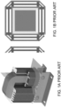
- FIG. 1A is a schematic perspective view of the medium voltage inductor of [Ref. 1]
- FIG. 1B is a schematic sectional view of the medium voltage inductor of FIG. 1 along plane AA'.
- the layer-to-layer insulation is achieved by providing spacers between the layers as shown in FIG. 1A and FIG. 1B .
- the voltage stress is handled by the air gap as well as the spacer.
- This method is simple and easy to implement but is not scalable to higher voltage. Also, it increases the volume of the inductor due to the large air gaps.
- an insulation material can also be used between the layers to reduce the spacing. However, such a structure does not offer a partial-discharge free operation to account for the air gaps between the windings.
- FIG. 2 shows an example of these structures.
- a medium voltage transformer is designed where the primary and secondary windings are separately dry cast to provide the required insulation.
- This concept can also be used for inductors where the inductor winding is dry cast and is placed at a certain distance from the core.
- a high frequency planar PCB transformer with medium voltage isolation is demonstrated.
- a dielectric material with a high breakdown voltage is used to withstand the medium voltage between primary and secondary windings.
- the core is encapsulated with an epoxy material, as well as moved away from the core to avoid partial discharge between the windings and the core. This structure, however, does not offer a partial discharge free operation at the interface of the low voltage and the medium voltage windings.
- these structures can be dipped into oil to achieve the required partial discharge ratings, but since dry type magnetics is preferred in the medium voltage applications, dipping the magnetics into oil does not provide the most effective and reliable solution.
- the present disclosure provides a reliable, potting free, partial discharge free at operating voltage, PCB-based solution, which can be manufactured easily with great repeatability and good performance.
- the present disclosure provides a PCB-based medium voltage inductor, including: a PCB having a through hole; a plurality of conductive layers embedded in the PCB and stacked on top of each other, the plurality of conductive layers being electrically connected with each other through one or more buried vias, each of the plurality of conductive layers being patterned to have a spiral shape around the central through hole and arranged in an annulus region having an annular radius; a first terminal electrically coupled to outermost ones of the plurality of conductive layers; and a second terminal electrically coupled to a centermost one of the plurality of conductive layers; wherein the plurality of conductive layers are arranged in a staggered pattern.
- the staggered pattern is a concave staggered pattern
- the concave staggered pattern is defined such that the annular radius of the plurality of conductive layers increases from the centermost one of the plurality of conductive layers to the outermost ones of the plurality of conductive layers.
- the plurality of conductive layers are spatially separated in a vertical direction.
- the PCB-based medium voltage inductor further includes a magnetic core magnetically coupled to the plurality of conductive layers, and the magnetic core has an air gap.
- the magnetic core is electrically connected to the first terminal or the second terminal.
- the PCB-based medium voltage inductor further includes a coating layer coated on a surface of the magnetic core, the coating layer is made of conducting or semiconducting material, and the magnetic core is electrically connected to the first terminal through the coating layer.
- each conductive layer is patterned to have a spiral shape around the through hole on a horizontal plane and to have plural revolutions, and corresponding revolutions of the plurality of conductive layers are aligned with each other, and sides of the corresponding revolutions of the plurality of conductive layers are arranged in the staggered pattern with a V-shape or a U-shape.
- the present disclosure provides a medium voltage inductor assembly, including: a plurality of the PCB-based medium voltage inductors discussed above; a bobbin structure that holds the PCB-based medium voltage inductors; and a magnetic core assembly magnetically coupled to the PCB-based medium voltage inductors.
- a window area is formed between the bobbin structure, the PCB-based medium voltage inductors and the magnetic core assembly, and the window area is configured to remove heat generated from plurality of conductive layers.
- the present disclosure provides a medium voltage inductor assembly, including a plurality of the PCB-based medium voltage inductor discussed above, wherein the first terminals of the PCB-based medium voltage inductors are electrically connected to each other, and wherein the second terminals of the PCB-based medium voltage inductors are electrically connected to each other.
- the present disclosure provides a PCB-based medium voltage inductor, including: a PCB having a through hole; a plurality of conductive layers embedded in the PCB and stacked on top of each other, the plurality of conductive layers being electrically connected with each other through one or more buried vias, each of the plurality of conductive layers being patterned to have a spiral shape around the through hole and arranged in an annulus region having an annular radius; a first terminal electrically coupled to outermost ones of the plurality of conductive layers; and a second terminal electrically coupled to a centermost one of the plurality of conductive layers; wherein the annular radius of the plurality of conductive layers increases from the centermost one of the plurality of conductive layers to the outermost ones of the plurality of conductive layers.
- the PCB-based medium voltage inductor further includes a winding extension protruding from an edge of the plurality of conductive layers, and the second terminal is electrically coupled to the centermost one of the plurality of conductive layers through the winding extension.
- the PCB-based medium voltage inductor further includes a winding extension protruding from an edge of the plurality of conductive layers, and lateral sides of the winding extension are arranged in a concave staggered pattern, and wherein a frontal side of the winding extension is arranged in a convex staggered pattern.
- the present disclosure provides a PCB-based medium voltage inductor, including: a PCB having a through hole; a plurality of conductive layers embedded in the PCB and stacked on top of each other, the plurality of conductive layers being electrically connected with each other through one or more buried vias, each of the plurality of conductive layers being patterned to have a spiral shape around the through hole and arranged in an annulus region having an annular radius; a winding extension protruding from an edge of the plurality of conductive layers; a first terminal electrically coupled to outermost ones of the plurality of conductive layers; and a second terminal electrically coupled to a centermost one of the plurality of conductive layers through the winding extension; wherein the annular radius of the plurality of conductive layers increases from the centermost one of the plurality of conductive layers to the outermost ones of the plurality of conductive layers.
- lateral sides of the winding extension are arranged in a concave staggered pattern, and a frontal side of the winding extension is arranged in a convex staggered pattern.
- the present disclosure is generally directed to a PCB-based medium voltage inductor, which offers a partial discharge free design without additional encapsulation.
- Embodiments of the present disclosure restrict the electric field on the surface of the PCB winding to less than the air breakdown voltage at operating voltage levels to create a partial discharge free operation.
- the magnetic core is tied to one of the terminals of the inductor to define the potential of the core, and thus shape the electric field at and/or near the surface of the PCB. It is to be understood that the PCB winding structure can be designed in any suitable manner to shape the electric field.
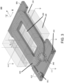
- FIG. 3 illustrates a PCB-based medium voltage inductor 300 in accordance with an embodiment of the present disclosure.
- Windings 310 of PCB-based medium voltage inductor 300 are embedded inside a PCB 305, while a magnetic core 320 provides a path for the magnetic field to flow.
- windings 310 may be made of copper or any other suitable conductive material including a plurality of conductive layers that are embedded in PCB 305 and stacked on top of each other. The conductive layers are electrically connected with each other using buried vias.
- a small air gap 330 is required in magnetic core 320 to achieve the required inductance.
- a through hole is provided in PCB 305 to accommodate magnetic core 320.
- the magnetic core 320 includes two E-shaped magnetic cores arranged in a mirror-image configuration vertically.
- the central magnetic pillars of the two E-shaped magnetic cores are accommodated within the through hole of PCB 305, and there are air gaps on the central magnetic pillars and side pillars of the two E-shaped magnetic cores.
- Each conductive layer of windings 310 may be patterned to have a spiral shape on a horizontal plane having several revolutions, such that it winds around the through hole of PCB 305 at a continuously increasing or decreasing distance.
- each spiral shaped conductive layer of windings 310 is confined within an oval or rectangular annulus region having an annulus radius.
- First and second terminals 301 and 302 are provided to direct electric current into and out of windings 310.
- first terminal 301 is electrically connected to the topmost and bottom most layers of windings 310
- second terminal 302 is electrically connected to the center most layer(s) of windings 310.
- PCB-based medium voltage inductor 300 includes two windings 310 connected with each other in parallel.
- PCB 305 can have any suitable shape and/or thickness. It should be noted that when a current/voltage is applied to PCB-based medium voltage inductor 300, the voltage will be distributed between windings 310, and thus forms a voltage gradient across the windings 310.
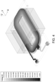
- FIG. 4 illustrates an exemplary voltage gradient in one conductive layer of PCB-based medium voltage inductor 300 when a 15 kV voltage is applied across first terminal 301 and second terminal 302.
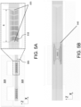
- FIGs. 5A, 5B , and 5C illustrate sectional views of PCB-based medium voltage inductor 300 along planes AA', BB', and CC' in FIG. 3 respectively.
- windings 310 of PCB-based medium voltage inductor 300 are arranged in a specific "staggered" pattern to limit or shape the electric field inside, on, and/or near PCB 305, thereby offering a partial discharge free operation of the PCB-based medium voltage inductor 300 without the need of any additional potting.
- windings 310 include twelve conductive layers (including the first to twelfth conductive layers from top to bottom), which are arranged in a "concave" staggered pattern.
- edges of the uppermost (e.g., the first conductive layer) and the lowermost (e.g., the twelfth conductive layer) layers of the conductive layers of windings 310 constitute a greater annulus radius R than that of the central layers (e.g., the sixth and seventh conductive layers).
- each revolution of the spiral shaped conductive layers is generally aligned with each other, except that when viewed in a sectional view from the sides (i.e., the sides of the revolutions), the first to twelfth conductive layers appear to form a concave (e.g., "V" or "U") shape. It is appreciated that any suitable quantity of conductive layers can be used depending on design choices.
- first to twelfth conductive layers of windings 310 are spatially separated in the vertical direction (or the Z direction) from each other using the PCB material and are electrically connected at specific points using buried vias (to provide a continuous current path).
- buried vias can be filled with an encapsulant material, such as epoxy, to avoid air bubbles inside the PCB material.
- the partial discharge free operation is made possible primarily because the voltage applied on first and second terminals 301 and 302 is distributed between windings 310, thereby forming a voltage gradient across windings 310.
- the staggered windings utilize this voltage gradient to shape the electric field inside and on the surface of PCB 305.
- the choice of the distance between the winding distances in the X direction is a design choice and can be changed depending on the requirement.
- FIGs. 5B and 5C focus on the region where an edge of the central conductive layers of windings 310 are protruded outward to form a winding extension 340 as shown in FIG. 3 for providing the necessary connection to a terminal (e.g., second terminal 302).
- a high electric field around this region may exceed the breakdown voltage of air and lead to partial discharges.
- an electric field limiting technique (such as staggering) is applied in this region of winding extension 340. Because different conductive layers of PCB-based medium voltage inductor 300 are at a different voltage due to the voltage gradient across windings 310 as shown in FIG.
- FIGs. 10A and 10B respectively illustrate computer simulated results of electric field distribution at a peak voltage of 15 kV for the conductive layers of a PCB-based medium voltage inductor arranged in "concave” and “convex” staggered patterns.
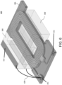
- FIG. 6 illustrates a PCB-based medium voltage inductor 600 in accordance with another embodiment of the present disclosure.
- PCB-based medium voltage inductor 600 in FIG. 6 is substantially identical to PCB-based medium voltage inductor 300 in FIG. 3 , except that magnetic core 320 is coated with a layer 610 of conductive or semiconductive material.
- electrical connection 620 is required between magnetic core 320 and one of the terminals (e.g., first terminal 301), because the staggered winding structure as shown in FIG. 6 can alleviate the electric field in the air to less than the air breakdown voltage only if magnetic core 320 is connected to one of the terminals.
- electrical connection 620 can be made using a conducting wire or a metal bar.
- the conducting/semiconducting coating (i.e., layer 610) on the surface of magnetic core 320 can provide a reliable connection for maintaining the potential of magnetic core 320.
- the electrical connection 620 should be made to both components of magnetic core 320.
- the choice of the terminal to which magnetic core 320 can be connected is not arbitrary. In one embodiment, magnetic core 320 should be connected to the terminal closest to the outer surface of PCB 305 (e.g., first terminal 301).
- FIG. 7 illustrates a cross-sectional view of a medium voltage inductor assembly 700 that uses a bobbin structure 730 to hold a plurality of PCB-based medium voltage inductors 711 and 712 and a magnetic core assembly 720 in accordance with an embodiment of the present disclosure.
- Bobbin structure 730 can be coated with a semi-conductive or conductive surface and can be electrically connected to magnetic core assembly 720 so that they share the same potential.
- the remaining window areas 740 can be used for forced air cooling solution to directly remove the heat generated from PCB-based medium voltage inductors 711 and 712.
- a thermally conductive material such as, aluminum nitride, can be coupled to PCB-based medium voltage inductors 711 and 712 with some thermal interface material to remove heat using heatsinks disposed on the thermally conductive material at a distance from medium voltage inductor assembly 700.
- FIG. 8 illustrates a medium voltage inductor assembly 800 including two identical PCB-based medium voltage inductors 810 and 820 connected in parallel in accordance with an embodiment of the present disclosure.
- first terminals 301 of PCB-based medium voltage inductors 810 and 820 are connected to each other, and second terminals 302 of PCB-based medium voltage inductors 810 and 820 are similarly connected.
- Paralleling two PCB-based medium voltage inductors reduces the current through each of the PCB-based medium voltage inductors, and thus can help to reduce the total winding losses.
- more PCB-based medium voltage inductors connected in parallel would require a larger window area, which increases the volume of the magnetic core as well as the overall size of the inductor. Optimization is required to establish the appropriate quantity of parallelly connected PCB-based medium voltage inductors for the desired medium voltage inductor assembly.
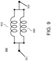
- FIG. 9 illustrates an equivalent circuit 900 for two parallelly connected PCB-based medium voltage inductors 910 and 920 in accordance with an embodiment of the present disclosure. More quantity of PCB-based medium voltage inductors can be connected in parallel depending on the window area available and/or required, which can help in reducing the total winding loss for the medium voltage inductor assembly.
Landscapes
- Engineering & Computer Science (AREA)
- Power Engineering (AREA)
- Microelectronics & Electronic Packaging (AREA)
- Coils Or Transformers For Communication (AREA)
- Coils Of Transformers For General Uses (AREA)
- Parts Printed On Printed Circuit Boards (AREA)
Abstract
Description
- The present disclosure relates to a printed circuit board (PCB) based planar winding structure for use in an inductor. More particularly, the present disclosure relates to a PCB-based planar winding structure for use in inductors for medium voltage applications.
- With the advancement of wide bandgap semiconductors, power electronic devices with high blocking voltages capable of switching at high frequencies have opened up new areas of applications and are becoming more common in the industry. These wide bandgap semiconductor-based converter systems find applications in power converters that includes but not limited to renewable energy integration, active filters, shore-to-ship power systems, and solid-state transformers. Solid-state transformers (SSTs) are considered the most lucrative solution to achieve all these requirements, because they can provide a direct power electronics interface from the medium voltage AC (MVac, 4.16 kV/13.8 kV grid) stage to the low voltage DC (LVdc, 400 V/800 V) stage. The major advantage of SSTs is that these SSTs eliminate the requirement of bulky conventional low-frequency transformers, which are replaced by high frequency magnetics and a power electronics interface. A typical connection from the MVac grid to a power electronics converter system requires a medium voltage inductor interface.
- MV inductors have been used in the power system since its inception. Conventionally, these inductors are designed for high power applications, and most importantly are used extensively for low frequency applications. Because these inductors are used for low frequency currents, silicon steel material is used as the core material along with solid copper windings. With SiC devices, however, the converters are operated at high switching frequencies to minimize the size of the magnetic components. Not only does this result in a low frequency current in the inductor, but also a high switching frequency ripple. Conventional medium voltage inductors fail in this scenario.
- A lot of research has been done predominantly in low voltage applications (i.e., < 2 kV) to account for these high frequency losses. The use of litz wires provides a good solution for decreasing the high frequency winding losses, and various core materials like ferrite or nanocrystalline can be used to reduce the high frequency core losses. However, medium voltage inductors require additional insulation, and necessitates a partial discharge free operation (reliable and continuous operation). Achieving a good efficiency and a reasonable power density along with the medium voltage insulation requirement remain as a big challenge. Also, considering the cost and ease of manufacturing, PCB based solutions are typically preferred over conventional winding-based solutions, because they offer reliable and repeatable designs.
- Various works have been done in the literature for medium voltage inductor design. Because high frequency medium voltage transformers have similar design criteria, they have also been included in the study. The major focus is on the insulation design of the inductors/transformers. The most basic method of achieving the required voltage insulation is by providing some distance between the windings and from layer-to-layer [Ref. 1]. In [Ref. 1], the medium voltage insulation between the winding and the core is achieved using a 3D printed bobbin.
FIG. 1A is a schematic perspective view of the medium voltage inductor of [Ref. 1], andFIG. 1B is a schematic sectional view of the medium voltage inductor ofFIG. 1 along plane AA'. The layer-to-layer insulation is achieved by providing spacers between the layers as shown inFIG. 1A and FIG. 1B . In this case, the voltage stress is handled by the air gap as well as the spacer. This method is simple and easy to implement but is not scalable to higher voltage. Also, it increases the volume of the inductor due to the large air gaps. It should be noted that instead of an air gap, an insulation material can also be used between the layers to reduce the spacing. However, such a structure does not offer a partial-discharge free operation to account for the air gaps between the windings. - Another method typically used for magnetics design is based on encapsulation or potting parts of the inductor using an encapsulating material. [Ref. 2] and [Ref. 3] provide a transformer/inductor design with this concept. A shielding layer may be added to the surface of this encapsulating structure to ensure that the electric field is limited within the encapsulant and thus the magnetic component can offer a partial discharge free behavior, as taught in [Ref. 4] and [Ref. 5]. However, in these structures, to achieve a partial discharge free operation, it is necessary to have an air-free space inside the encapsulating structure. This is rather difficult and unreliable to achieve especially when a multi-layer winding structure is used.
FIG. 2 shows an example of these structures. - In [Ref. 6], a medium voltage transformer is designed where the primary and secondary windings are separately dry cast to provide the required insulation. This concept can also be used for inductors where the inductor winding is dry cast and is placed at a certain distance from the core.
- Another method is showcased in [Ref. 7], where a medium voltage air core transformer is demonstrated. This concept can also be extended for air core inductors. In terms of insulation, this structure proves to be beneficial due to the absence of the core, which removes any restrictions for the winding to core insulation. While this is beneficial in terms of insulation design to a certain extent, it is not feasible to use air core-based inductors in various applications, due to its largely increased size and undirected magnetic fields, which is a consequence of the absence of core. Also, it is impractical to scale the concept for higher value of inductances. For these reasons, air core magnetics are typically not preferred in most applications.
- In [Ref. 8], a high frequency planar PCB transformer with medium voltage isolation is demonstrated. A dielectric material with a high breakdown voltage is used to withstand the medium voltage between primary and secondary windings. To avoid arcing from the edge of the windings to the core, the core is encapsulated with an epoxy material, as well as moved away from the core to avoid partial discharge between the windings and the core. This structure, however, does not offer a partial discharge free operation at the interface of the low voltage and the medium voltage windings.
- Typically, these structures can be dipped into oil to achieve the required partial discharge ratings, but since dry type magnetics is preferred in the medium voltage applications, dipping the magnetics into oil does not provide the most effective and reliable solution.
-
- [Ref. 1] H. Zhao et al., "Physics-Based Modeling of Parasitic Capacitance in Medium-Voltage Filter Inductors," IEEE Transactions on Power Electronics, vol. 36, no. 1, pp. 829-843, Jan. 2021, doi: 10.1109/TPEL.2020.3003157.
- [Ref. 2] D. Rothmund, T. Guillod, D. Bortis and J. W. Kolar, "99% Efficient 10 kV SiC-Based 7 kV/400 V DC Transformer for Future Data Centers," IEEE Journal of Emerging and Selected Topics in Power Electronics, vol. 7, no. 2, pp. 753-767, June 2019, doi: 10.1109/JESTPE.2018.2886139.
- [Ref. 3] D. Rothmund, T. Guillod, D. Bortis and J. W. Kolar, "99.1% Efficient 10 kV SiC-Based Medium-Voltage ZVS Bidirectional Single-Phase PFC AC/DC Stage," IEEE Journal of Emerging and Selected Topics in Power Electronics, vol. 7, no. 2, pp. 779-797, June 2019, doi: 10.1109/JESTPE.2018.2886140.
- [Ref. 4] H. Li, P. Yao, Z. Gao and F. Wang, "Medium Voltage Converter Inductor Insulation Design Considering Grid Requirements," IEEE Journal of Emerging and Selected Topics in Power Electronics, vol. 10, no. 2, pp. 2339-2350, April 2022, doi: 10.1109/JESTPE.2021.3131602.
- [Ref. 5] Q. Chen, R. Raju, D. Dong and M. Agamy, "High Frequency Transformer Insulation in Medium Voltage SiC enabled Air-cooled Solid-State Transformers," 2018 IEEE Energy Conversion Congress and Exposition (ECCE), 2018, pp. 2436-2443, doi: 10.1109/ECCE.2018.8557849.
- [Ref. 6] T. B. Gradinger, U. Drofenik and S. Alvarez, "Novel insulation concept for an MV dry-cast medium-frequency transformer," 2017 19th European Conference on Power Electronics and Applications (EPE'17 ECCE Europe), 2017, pp. P.1-P.10, doi: 10.23919/EPE17ECCEEurope.2017.8099006.
- [Ref. 7] P. Czyz, T. Guillod, F. Krismer, J. Huber and J. W. Kolar, "Design and Experimental Analysis of 166 kW Medium-Voltage Medium-Frequency Air-Core Transformer for 1:1-DCX Applications," IEEE Journal of Emerging and Selected Topics in Power Electronics, doi: 10.1109/JESTPE.2021.3060506.
- [Ref. 8] S. Mukherjee et al., "A High-Frequency Planar Transformer with Medium-Voltage Isolation," 2021 IEEE Applied Power Electronics Conference and Exposition (APEC), 2021, pp. 2065-2070, doi: 10.1109/APEC42165.2021.9487061.
- The present disclosure provides a reliable, potting free, partial discharge free at operating voltage, PCB-based solution, which can be manufactured easily with great repeatability and good performance.
- In one aspect, the present disclosure provides a PCB-based medium voltage inductor, including: a PCB having a through hole; a plurality of conductive layers embedded in the PCB and stacked on top of each other, the plurality of conductive layers being electrically connected with each other through one or more buried vias, each of the plurality of conductive layers being patterned to have a spiral shape around the central through hole and arranged in an annulus region having an annular radius; a first terminal electrically coupled to outermost ones of the plurality of conductive layers; and a second terminal electrically coupled to a centermost one of the plurality of conductive layers; wherein the plurality of conductive layers are arranged in a staggered pattern.
- In one embodiment, the staggered pattern is a concave staggered pattern, and the concave staggered pattern is defined such that the annular radius of the plurality of conductive layers increases from the centermost one of the plurality of conductive layers to the outermost ones of the plurality of conductive layers.
- In one embodiment, the plurality of conductive layers are spatially separated in a vertical direction.
- In one embodiment, the PCB-based medium voltage inductor further includes a magnetic core magnetically coupled to the plurality of conductive layers, and the magnetic core has an air gap.
- In one embodiment, the magnetic core is electrically connected to the first terminal or the second terminal.
- In one embodiment, the PCB-based medium voltage inductor further includes a coating layer coated on a surface of the magnetic core, the coating layer is made of conducting or semiconducting material, and the magnetic core is electrically connected to the first terminal through the coating layer.
- In one embodiment, each conductive layer is patterned to have a spiral shape around the through hole on a horizontal plane and to have plural revolutions, and corresponding revolutions of the plurality of conductive layers are aligned with each other, and sides of the corresponding revolutions of the plurality of conductive layers are arranged in the staggered pattern with a V-shape or a U-shape.
- In another aspect, the present disclosure provides a medium voltage inductor assembly, including: a plurality of the PCB-based medium voltage inductors discussed above; a bobbin structure that holds the PCB-based medium voltage inductors; and a magnetic core assembly magnetically coupled to the PCB-based medium voltage inductors.
- In one embodiment, a window area is formed between the bobbin structure, the PCB-based medium voltage inductors and the magnetic core assembly, and the window area is configured to remove heat generated from plurality of conductive layers.
- In still another aspect, the present disclosure provides a medium voltage inductor assembly, including a plurality of the PCB-based medium voltage inductor discussed above, wherein the first terminals of the PCB-based medium voltage inductors are electrically connected to each other, and wherein the second terminals of the PCB-based medium voltage inductors are electrically connected to each other.
- In yet another aspect, the present disclosure provides a PCB-based medium voltage inductor, including: a PCB having a through hole; a plurality of conductive layers embedded in the PCB and stacked on top of each other, the plurality of conductive layers being electrically connected with each other through one or more buried vias, each of the plurality of conductive layers being patterned to have a spiral shape around the through hole and arranged in an annulus region having an annular radius; a first terminal electrically coupled to outermost ones of the plurality of conductive layers; and a second terminal electrically coupled to a centermost one of the plurality of conductive layers; wherein the annular radius of the plurality of conductive layers increases from the centermost one of the plurality of conductive layers to the outermost ones of the plurality of conductive layers.
- In one embodiment, the PCB-based medium voltage inductor further includes a winding extension protruding from an edge of the plurality of conductive layers, and the second terminal is electrically coupled to the centermost one of the plurality of conductive layers through the winding extension.
- In one embodiment, the PCB-based medium voltage inductor further includes a winding extension protruding from an edge of the plurality of conductive layers, and lateral sides of the winding extension are arranged in a concave staggered pattern, and wherein a frontal side of the winding extension is arranged in a convex staggered pattern.
- In a further aspect, the present disclosure provides a PCB-based medium voltage inductor, including: a PCB having a through hole; a plurality of conductive layers embedded in the PCB and stacked on top of each other, the plurality of conductive layers being electrically connected with each other through one or more buried vias, each of the plurality of conductive layers being patterned to have a spiral shape around the through hole and arranged in an annulus region having an annular radius; a winding extension protruding from an edge of the plurality of conductive layers; a first terminal electrically coupled to outermost ones of the plurality of conductive layers; and a second terminal electrically coupled to a centermost one of the plurality of conductive layers through the winding extension; wherein the annular radius of the plurality of conductive layers increases from the centermost one of the plurality of conductive layers to the outermost ones of the plurality of conductive layers.
- In one embodiment, lateral sides of the winding extension are arranged in a concave staggered pattern, and a frontal side of the winding extension is arranged in a convex staggered pattern.
- The present disclosure is better understood upon consideration of the following detailed description and the accompanying figures.
-
FIG. 1A and FIG. 1B illustrate a conventional transformer solution that achieves insulation by providing space between the windings and between the winding and the core. -
FIG. 2 illustrates a conventional transformer solution with an encapsulant to seal the windings and a shielding layer on the encapsulant. -
FIG. 3 illustrates a PCB-based medium voltage inductor in accordance with an embodiment of the present disclosure. -
FIG. 4 illustrates an exemplary voltage gradient in one layer of the PCB-based medium voltage inductor ofFIG. 3 , when a 15 kV voltage is applied across electric terminals of the PCB-based medium voltage inductor. -
FIGs. 5A, 5B , and5C respectively illustrate a sectional view of the PCB-based medium voltage inductor ofFIG. 3 along planes AA', BB', and CC'. -
FIG. 6 illustrates a PCB-based medium voltage inductor in accordance with another embodiment of the present disclosure. -
FIG. 7 illustrates a cross-sectional view of a PCB-based medium voltage inductor that uses a bobbin structure to hold a plurality of PCB windings and a magnetic core assembly in accordance with an embodiment of the present disclosure. -
FIG. 8 illustrates a PCB-based medium voltage inductor assembly including two identical PCB-based inductors connected in parallel in accordance with an embodiment of the present disclosure. -
FIG. 9 illustrates an equivalent circuit for two parallelly connected PCB-based windings in accordance with an embodiment of the present disclosure. -
FIGs. 10A and10B respectively illustrate simulated results of electric field distribution for the conductive layers of a PCB-based medium voltage inductor arranged in "concave" and "convex" staggered patterns. - The present disclosure is generally directed to a PCB-based medium voltage inductor, which offers a partial discharge free design without additional encapsulation. Embodiments of the present disclosure restrict the electric field on the surface of the PCB winding to less than the air breakdown voltage at operating voltage levels to create a partial discharge free operation. The magnetic core is tied to one of the terminals of the inductor to define the potential of the core, and thus shape the electric field at and/or near the surface of the PCB. It is to be understood that the PCB winding structure can be designed in any suitable manner to shape the electric field.
-
FIG. 3 illustrates a PCB-basedmedium voltage inductor 300 in accordance with an embodiment of the present disclosure.Windings 310 of PCB-basedmedium voltage inductor 300 are embedded inside aPCB 305, while amagnetic core 320 provides a path for the magnetic field to flow. In certain embodiments,windings 310 may be made of copper or any other suitable conductive material including a plurality of conductive layers that are embedded inPCB 305 and stacked on top of each other. The conductive layers are electrically connected with each other using buried vias. Asmall air gap 330 is required inmagnetic core 320 to achieve the required inductance. A through hole is provided inPCB 305 to accommodatemagnetic core 320. Themagnetic core 320 includes two E-shaped magnetic cores arranged in a mirror-image configuration vertically. The central magnetic pillars of the two E-shaped magnetic cores are accommodated within the through hole ofPCB 305, and there are air gaps on the central magnetic pillars and side pillars of the two E-shaped magnetic cores. - Each conductive layer of
windings 310 may be patterned to have a spiral shape on a horizontal plane having several revolutions, such that it winds around the through hole ofPCB 305 at a continuously increasing or decreasing distance. In one embodiment, each spiral shaped conductive layer ofwindings 310 is confined within an oval or rectangular annulus region having an annulus radius. - First and
second terminals windings 310. In one embodiment,first terminal 301 is electrically connected to the topmost and bottom most layers ofwindings 310, whilesecond terminal 302 is electrically connected to the center most layer(s) ofwindings 310. Essentially, PCB-basedmedium voltage inductor 300 includes twowindings 310 connected with each other in parallel. - Depending on specific designs and/or requirements,
PCB 305 can have any suitable shape and/or thickness. It should be noted that when a current/voltage is applied to PCB-basedmedium voltage inductor 300, the voltage will be distributed betweenwindings 310, and thus forms a voltage gradient across thewindings 310.FIG. 4 illustrates an exemplary voltage gradient in one conductive layer of PCB-basedmedium voltage inductor 300 when a 15 kV voltage is applied acrossfirst terminal 301 andsecond terminal 302. -
FIGs. 5A, 5B , and5C illustrate sectional views of PCB-basedmedium voltage inductor 300 along planes AA', BB', and CC' inFIG. 3 respectively. As shown inFIG. 5A ,windings 310 of PCB-basedmedium voltage inductor 300 are arranged in a specific "staggered" pattern to limit or shape the electric field inside, on, and/or nearPCB 305, thereby offering a partial discharge free operation of the PCB-basedmedium voltage inductor 300 without the need of any additional potting. In this embodiment,windings 310 include twelve conductive layers (including the first to twelfth conductive layers from top to bottom), which are arranged in a "concave" staggered pattern. That is, edges of the uppermost (e.g., the first conductive layer) and the lowermost (e.g., the twelfth conductive layer) layers of the conductive layers ofwindings 310 constitute a greater annulus radius R than that of the central layers (e.g., the sixth and seventh conductive layers). In addition, each revolution of the spiral shaped conductive layers is generally aligned with each other, except that when viewed in a sectional view from the sides (i.e., the sides of the revolutions), the first to twelfth conductive layers appear to form a concave (e.g., "V" or "U") shape. It is appreciated that any suitable quantity of conductive layers can be used depending on design choices. In addition, the first to twelfth conductive layers ofwindings 310 are spatially separated in the vertical direction (or the Z direction) from each other using the PCB material and are electrically connected at specific points using buried vias (to provide a continuous current path). These buried vias can be filled with an encapsulant material, such as epoxy, to avoid air bubbles inside the PCB material. - It is appreciated that the partial discharge free operation is made possible primarily because the voltage applied on first and
second terminals windings 310, thereby forming a voltage gradient acrosswindings 310. The staggered windings utilize this voltage gradient to shape the electric field inside and on the surface ofPCB 305. The choice of the distance between the winding distances in the X direction is a design choice and can be changed depending on the requirement. -
FIGs. 5B and5C focus on the region where an edge of the central conductive layers ofwindings 310 are protruded outward to form a windingextension 340 as shown inFIG. 3 for providing the necessary connection to a terminal (e.g., second terminal 302). A high electric field around this region may exceed the breakdown voltage of air and lead to partial discharges. To prevent such a strong electric field, an electric field limiting technique (such as staggering) is applied in this region of windingextension 340. Because different conductive layers of PCB-basedmedium voltage inductor 300 are at a different voltage due to the voltage gradient acrosswindings 310 as shown inFIG. 4 , individual layers are extended to form an equipotential surface on each layer, and these extensions are designed in a certain way to limit the electric field in the region. In one embodiment, lateral sides of windingextension 340 are arranged in a "concave" staggered pattern as shown inFIG. 5B , while a frontal side of windingextension 340 is arranged in a "convex" staggered pattern as shown inFIG. 5C .FIGs. 10A and10B respectively illustrate computer simulated results of electric field distribution at a peak voltage of 15 kV for the conductive layers of a PCB-based medium voltage inductor arranged in "concave" and "convex" staggered patterns. -
FIG. 6 illustrates a PCB-basedmedium voltage inductor 600 in accordance with another embodiment of the present disclosure. PCB-basedmedium voltage inductor 600 inFIG. 6 is substantially identical to PCB-basedmedium voltage inductor 300 inFIG. 3 , except thatmagnetic core 320 is coated with alayer 610 of conductive or semiconductive material. In addition,electrical connection 620 is required betweenmagnetic core 320 and one of the terminals (e.g., first terminal 301), because the staggered winding structure as shown inFIG. 6 can alleviate the electric field in the air to less than the air breakdown voltage only ifmagnetic core 320 is connected to one of the terminals. In certain embodiments,electrical connection 620 can be made using a conducting wire or a metal bar. The conducting/semiconducting coating (i.e., layer 610) on the surface ofmagnetic core 320 can provide a reliable connection for maintaining the potential ofmagnetic core 320. It should be noted that theelectrical connection 620 should be made to both components ofmagnetic core 320. The choice of the terminal to whichmagnetic core 320 can be connected is not arbitrary. In one embodiment,magnetic core 320 should be connected to the terminal closest to the outer surface of PCB 305 (e.g., first terminal 301). -
FIG. 7 illustrates a cross-sectional view of a mediumvoltage inductor assembly 700 that uses abobbin structure 730 to hold a plurality of PCB-basedmedium voltage inductors magnetic core assembly 720 in accordance with an embodiment of the present disclosure. Bobbinstructure 730 can be coated with a semi-conductive or conductive surface and can be electrically connected tomagnetic core assembly 720 so that they share the same potential. Also, because mediumvoltage inductor assembly 700 is a potting-less solution, the remainingwindow areas 740 can be used for forced air cooling solution to directly remove the heat generated from PCB-basedmedium voltage inductors medium voltage inductors voltage inductor assembly 700. -
FIG. 8 illustrates a mediumvoltage inductor assembly 800 including two identical PCB-basedmedium voltage inductors first terminals 301 of PCB-basedmedium voltage inductors second terminals 302 of PCB-basedmedium voltage inductors -
FIG. 9 illustrates anequivalent circuit 900 for two parallelly connected PCB-basedmedium voltage inductors
Claims (15)
- A PCB-based medium voltage inductor (300), characterized by comprising:a PCB (305) having a through hole;a plurality of conductive layers embedded in the PCB (305) and stacked on top of each other, the plurality of conductive layers being electrically connected with each other through one or more buried vias, each of the plurality of conductive layers being patterned to have a spiral shape around the through hole and arranged in an annulus region having an annular radius;a first terminal (301) electrically coupled to outermost ones of the plurality of conductive layers; anda second terminal (302) electrically coupled to a centermost one of the plurality of conductive layers;wherein the plurality of conductive layers are arranged in a staggered pattern.
- The PCB-based medium voltage inductor (300) of claim 1, wherein the staggered pattern is a concave staggered pattern, and the concave staggered pattern is defined such that the annular radius of the plurality of conductive layers increases from the centermost one of the plurality of conductive layers to the outermost ones of the plurality of conductive layers.
- The PCB-based medium voltage inductor (300) of claim 1, wherein the plurality of conductive layers are spatially separated in a vertical direction.
- The PCB-based medium voltage inductor (300) of claim 1, further comprising a magnetic core (320) magnetically coupled to the plurality of conductive layers, wherein the magnetic core (320) has an air gap (330).
- The PCB-based medium voltage inductor (300) of claim 4, wherein the magnetic core (320) is electrically connected to the first terminal (301) or the second terminal (302).
- The PCB-based medium voltage inductor (600) of claim 5, further comprising a coating layer (610) coated on a surface of the magnetic core (320), wherein the coating layer (610) is made of conducting or semiconducting material, and the magnetic core (320) is electrically connected to the first terminal (301) through the coating layer (610).
- The PCB-based medium voltage inductor (300) of claim 1, wherein each of the plurality of conductive layers is patterned to have a spiral shape around the through hole on a horizontal plane and to have plural revolutions, corresponding revolutions of the plurality of conductive layers are aligned with each other, and sides of the corresponding revolutions of the plurality of conductive layers are arranged in the staggered pattern with a V-shape or a U-shape.
- A medium voltage inductor assembly (700), characterized by comprising:a plurality of the PCB-based medium voltage inductors according to claim 1;a bobbin structure (730) that holds the PCB-based medium voltage inductors; anda magnetic core assembly (720) magnetically coupled to the PCB-based medium voltage inductors.
- The medium voltage inductor assembly (700) of claim 8, wherein a window area (740) is formed between the bobbin structure (730), the PCB-based medium voltage inductors and the magnetic core assembly (720), and the window area (740) is configured to remove heat generated from plurality of conductive layers.
- A medium voltage inductor assembly (800), characterized by comprising a plurality of the PCB-based medium voltage inductors according to claim 1, wherein the first terminals of the PCB-based medium voltage inductors are electrically connected to each other, and wherein the second terminals of the PCB-based medium voltage inductors are electrically connected to each other.
- A PCB-based medium voltage inductor (300), characterized by comprising:a PCB (305) having a through hole;a plurality of conductive layers embedded in the PCB (305) and stacked on top of each other, the plurality of conductive layers being electrically connected with each other through one or more buried vias, each of the plurality of conductive layers being patterned to have a spiral shape around the through hole and arranged in an annulus region having an annular radius;a first terminal (301) electrically coupled to outermost ones of the plurality of conductive layers; anda second terminal (302) electrically coupled to a centermost one of the plurality of conductive layers;wherein the annular radius of the plurality of conductive layers increases from the centermost one of the plurality of conductive layers to the outermost ones of the plurality of conductive layers.
- The PCB-based medium voltage inductor (300) of claim 1 or 11, further comprising a winding extension (340) protruding from an edge of the plurality of conductive layers, wherein the second terminal (302) is electrically coupled to the centermost one of the plurality of conductive layers through the winding extension (340).
- The PCB-based medium voltage inductor (300) of claim 1 or 11, further comprising a winding extension (340) protruding from an edge of the plurality of conductive layers, wherein lateral sides of the winding extension (340) are arranged in a concave staggered pattern, and wherein a frontal side of the winding extension (340) is arranged in a convex staggered pattern.
- A PCB-based medium voltage inductor (300), characterized by comprising:a PCB (305) having a through hole;a plurality of conductive layers embedded in the PCB (305) and stacked on top of each other, the plurality of conductive layers being electrically connected with each other through one or more buried vias, each of the plurality of conductive layers being patterned to have a spiral shape around the through hole and arranged in an annulus region having an annular radius;a winding extension (340) protruding from an edge of the plurality of conductive layers;a first terminal (301) electrically coupled to outermost ones of the plurality of conductive layers; anda second terminal (302) electrically coupled to a centermost one of the plurality of conductive layers through the winding extension (340);wherein the annular radius of the plurality of conductive layers increases from the centermost one of the plurality of conductive layers to the outermost ones of the plurality of conductive layers.
- The PCB-based medium voltage inductor (300) of claim 14, wherein lateral sides of the winding extension (340) are arranged in a concave staggered pattern, and a frontal side of the winding extension (340) is arranged in a convex staggered pattern.
Applications Claiming Priority (1)
| Application Number | Priority Date | Filing Date | Title |
|---|---|---|---|
| US18/316,219 US20240379278A1 (en) | 2023-05-11 | 2023-05-11 | Printed circuit board based winding structure for inductors |
Publications (2)
| Publication Number | Publication Date |
|---|---|
| EP4462455A2 true EP4462455A2 (en) | 2024-11-13 |
| EP4462455A3 EP4462455A3 (en) | 2025-02-05 |
Family
ID=90925089
Family Applications (1)
| Application Number | Title | Priority Date | Filing Date |
|---|---|---|---|
| EP24173398.9A Pending EP4462455A3 (en) | 2023-05-11 | 2024-04-30 | Printed circuit board based winding structure for inductors |
Country Status (4)
| Country | Link |
|---|---|
| US (1) | US20240379278A1 (en) |
| EP (1) | EP4462455A3 (en) |
| JP (1) | JP7783332B2 (en) |
| CN (1) | CN118942868A (en) |
Family Cites Families (8)
| Publication number | Priority date | Publication date | Assignee | Title |
|---|---|---|---|---|
| JPS58124916U (en) * | 1982-02-17 | 1983-08-25 | オリンパス光学工業株式会社 | Laminated printed coil |
| JPH09260144A (en) * | 1996-03-22 | 1997-10-03 | Matsushita Electric Ind Co Ltd | Coil component and method of manufacturing the same |
| JP3731272B2 (en) * | 1997-01-10 | 2006-01-05 | 株式会社村田製作所 | Multilayer inductor |
| JP3798344B2 (en) * | 2002-06-14 | 2006-07-19 | 三菱電機株式会社 | Transformer for vehicle |
| JP2008300734A (en) * | 2007-06-01 | 2008-12-11 | Mitsubishi Electric Corp | Printed circuit board and manufacturing method thereof |
| JP2012134291A (en) * | 2010-12-21 | 2012-07-12 | Sanken Electric Co Ltd | Electronic circuit device |
| CN216287941U (en) * | 2021-12-13 | 2022-04-12 | 上海迈相电源技术有限公司 | Planar transformer or planar inductor |
| CN114188135B (en) * | 2021-12-14 | 2025-04-08 | 中国科学院电工研究所 | High-voltage isolation flat-plate transformer based on guiding equipotential lines and optimization method thereof |
-
2023
- 2023-05-11 US US18/316,219 patent/US20240379278A1/en active Pending
-
2024
- 2024-04-29 CN CN202410527997.XA patent/CN118942868A/en active Pending
- 2024-04-30 EP EP24173398.9A patent/EP4462455A3/en active Pending
- 2024-05-01 JP JP2024074524A patent/JP7783332B2/en active Active
Non-Patent Citations (8)
| Title |
|---|
| D. ROTHMUNDT. GUILLODD. BORTISJ. W. KOLAR: "99% Efficient 10 kV SiC-Based 7 kV/400 V DC Transformer for Future Data Centers", IEEE JOURNAL OF EMERGING AND SELECTED TOPICS IN POWER ELECTRONICS, vol. 7, no. 2, June 2019 (2019-06-01), pages 753 - 767, XP011722538, DOI: 10.1109/JESTPE.2018.2886139 |
| D. ROTHMUNDT. GUILLODD. BORTISJ. W. KOLAR: "99.1% Efficient 10 kV SiC-Based Medium-Voltage ZVS Bidirectional Single-Phase PFC AC/DC Stage", IEEE JOURNAL OF EMERGING AND SELECTED TOPICS IN POWER ELECTRONICS, vol. 7, no. 2, June 2019 (2019-06-01), pages 779 - 797, XP011722540, DOI: 10.1109/JESTPE.2018.2886140 |
| H. LIP. YAOZ. GAOF. WANG: "Medium Voltage Converter Inductor Insulation Design Considering Grid Requirements", IEEE JOURNAL OF EMERGING AND SELECTED TOPICS IN POWER ELECTRONICS, vol. 10, no. 2, April 2022 (2022-04-01), pages 2339 - 2350 |
| H. ZHAO ET AL.: "Physics-Based Modeling of Parasitic Capacitance in Medium-Voltage Filter Inductors", IEEE TRANSACTIONS ON POWER ELECTRONICS, vol. 36, no. 1, January 2021 (2021-01-01), pages 829 - 843, XP011808059, DOI: 10.1109/TPEL.2020.3003157 |
| P. CZYZT. GUILLODF. KRISMERJ. HUBERJ. W. KOLAR: "Design and Experimental Analysis of 166 kW Medium-Voltage Medium-Frequency Air-Core Transformer for El-DCX Applications", IEEE JOURNAL OF EMERGING AND SELECTED TOPICS IN POWER ELECTRONICS |
| Q. CHENR. RAJUD. DONGM. AGAMY: "High Frequency Transformer Insulation in Medium Voltage SiC enabled Air-cooled Solid-State Transformers", IEEE ENERGY CONVERSION CONGRESS AND EXPOSITION (ECCE, 2018, pages 2436 - 2443, XP033463917, DOI: 10.1109/ECCE.2018.8557849 |
| S. MUKHERJEE ET AL.: "A High-Frequency Planar Transformer with Medium-Voltage Isolation", 2021 IEEE APPLIED POWER ELECTRONICS CONFERENCE AND EXPOSITION (APEC, 2021, pages 2065 - 2070, XP033944695, DOI: 10.1109/APEC42165.2021.9487061 |
| T. B. GRADINGERU. DROFENIKS. ALVAREZ: "Novel insulation concept for an MV dry-cast medium-frequency transformer", 2017 19TH EUROPEAN CONFERENCE ON POWER ELECTRONICS AND APPLICATIONS (EPE'17 ECCE EUROPE, 2017, pages 1 - 10 |
Also Published As
| Publication number | Publication date |
|---|---|
| JP7783332B2 (en) | 2025-12-09 |
| EP4462455A3 (en) | 2025-02-05 |
| CN118942868A (en) | 2024-11-12 |
| TW202445613A (en) | 2024-11-16 |
| US20240379278A1 (en) | 2024-11-14 |
| JP2024163049A (en) | 2024-11-21 |
Similar Documents
| Publication | Publication Date | Title |
|---|---|---|
| US6181231B1 (en) | Diamond-based transformers and power convertors | |
| US8816808B2 (en) | Method and apparatus for cooling an annular inductor | |
| US8624702B2 (en) | Inductor mounting apparatus and method of use thereof | |
| US8373530B2 (en) | Power converter method and apparatus | |
| EP2444983A2 (en) | Liquid cooled magnetic component with indirect cooling for high frequency and high power applications | |
| US8629746B2 (en) | High frequency transformers | |
| US8130069B1 (en) | Distributed gap inductor apparatus and method of use thereof | |
| US8125777B1 (en) | Methods and apparatus for electrical components | |
| US20220037080A1 (en) | Shielding arrangements for transformer structures | |
| US20060279394A1 (en) | Terminal system for planar magnetics assembly | |
| CN111899964B (en) | Multi-winding high-frequency transformer with solid insulation structure | |
| WO2014006107A1 (en) | Transformer | |
| US12451286B2 (en) | Planar winding structure for power transformer | |
| CN114424304A (en) | Winding arrangement as part of an integrated structure for an intermediate frequency transformer | |
| US20230170125A1 (en) | Inductor | |
| US20240379278A1 (en) | Printed circuit board based winding structure for inductors | |
| Anurag et al. | Pcb based inductor structure for mv applications | |
| TWI916816B (en) | Pcb-based medium voltage inductor and medium voltage inductor assembly | |
| Ramakrishnan et al. | A comparison study of low-profile power magnetics for high-frequency, high-density switching converters | |
| EP4160631A1 (en) | Planar winding structure for power transformer | |
| JP7300381B2 (en) | Transformer and power converter using the same | |
| CN116246880A (en) | A Very Low Leakage Inductance Flyback Transformer Winding Method | |
| US20250174389A1 (en) | Inductor structure for medium voltage insulation | |
| WO2016005537A2 (en) | Inductor structure for multi-phase power conversion | |
| CN219066578U (en) | Magnetic components and power electronic transformers |
Legal Events
| Date | Code | Title | Description |
|---|---|---|---|
| PUAI | Public reference made under article 153(3) epc to a published international application that has entered the european phase |
Free format text: ORIGINAL CODE: 0009012 |
|
| STAA | Information on the status of an ep patent application or granted ep patent |
Free format text: STATUS: THE APPLICATION HAS BEEN PUBLISHED |
|
| AK | Designated contracting states |
Kind code of ref document: A2 Designated state(s): AL AT BE BG CH CY CZ DE DK EE ES FI FR GB GR HR HU IE IS IT LI LT LU LV MC ME MK MT NL NO PL PT RO RS SE SI SK SM TR |
|
| PUAL | Search report despatched |
Free format text: ORIGINAL CODE: 0009013 |
|
| AK | Designated contracting states |
Kind code of ref document: A3 Designated state(s): AL AT BE BG CH CY CZ DE DK EE ES FI FR GB GR HR HU IE IS IT LI LT LU LV MC ME MK MT NL NO PL PT RO RS SE SI SK SM TR |
|
| RIC1 | Information provided on ipc code assigned before grant |
Ipc: H01F 27/34 20060101ALI20250102BHEP Ipc: H01F 27/29 20060101ALI20250102BHEP Ipc: H01F 17/04 20060101ALI20250102BHEP Ipc: H01F 17/00 20060101AFI20250102BHEP |
|
| STAA | Information on the status of an ep patent application or granted ep patent |
Free format text: STATUS: REQUEST FOR EXAMINATION WAS MADE |
|
| 17P | Request for examination filed |
Effective date: 20250804 |