EP4461709A1 - Method of manufacturing display device - Google Patents
Method of manufacturing display device Download PDFInfo
- Publication number
- EP4461709A1 EP4461709A1 EP24166599.1A EP24166599A EP4461709A1 EP 4461709 A1 EP4461709 A1 EP 4461709A1 EP 24166599 A EP24166599 A EP 24166599A EP 4461709 A1 EP4461709 A1 EP 4461709A1
- Authority
- EP
- European Patent Office
- Prior art keywords
- glass
- gls
- forming
- layer
- display device
- Prior art date
- Legal status (The legal status is an assumption and is not a legal conclusion. Google has not performed a legal analysis and makes no representation as to the accuracy of the status listed.)
- Pending
Links
Images





Classifications
-
- C—CHEMISTRY; METALLURGY
- C03—GLASS; MINERAL OR SLAG WOOL
- C03C—CHEMICAL COMPOSITION OF GLASSES, GLAZES OR VITREOUS ENAMELS; SURFACE TREATMENT OF GLASS; SURFACE TREATMENT OF FIBRES OR FILAMENTS MADE FROM GLASS, MINERALS OR SLAGS; JOINING GLASS TO GLASS OR OTHER MATERIALS
- C03C15/00—Surface treatment of glass, not in the form of fibres or filaments, by etching
-
- H—ELECTRICITY
- H10—SEMICONDUCTOR DEVICES; ELECTRIC SOLID-STATE DEVICES NOT OTHERWISE PROVIDED FOR
- H10D—INORGANIC ELECTRIC SEMICONDUCTOR DEVICES
- H10D86/00—Integrated devices formed in or on insulating or conducting substrates, e.g. formed in silicon-on-insulator [SOI] substrates or on stainless steel or glass substrates
- H10D86/01—Manufacture or treatment
- H10D86/021—Manufacture or treatment of multiple TFTs
- H10D86/0212—Manufacture or treatment of multiple TFTs comprising manufacture, treatment or coating of substrates
-
- B—PERFORMING OPERATIONS; TRANSPORTING
- B24—GRINDING; POLISHING
- B24C—ABRASIVE OR RELATED BLASTING WITH PARTICULATE MATERIAL
- B24C1/00—Methods for use of abrasive blasting for producing particular effects; Use of auxiliary equipment in connection with such methods
- B24C1/04—Methods for use of abrasive blasting for producing particular effects; Use of auxiliary equipment in connection with such methods for treating only selected parts of a surface, e.g. for carving stone or glass
-
- C—CHEMISTRY; METALLURGY
- C03—GLASS; MINERAL OR SLAG WOOL
- C03C—CHEMICAL COMPOSITION OF GLASSES, GLAZES OR VITREOUS ENAMELS; SURFACE TREATMENT OF GLASS; SURFACE TREATMENT OF FIBRES OR FILAMENTS MADE FROM GLASS, MINERALS OR SLAGS; JOINING GLASS TO GLASS OR OTHER MATERIALS
- C03C17/00—Surface treatment of glass, not in the form of fibres or filaments, by coating
- C03C17/22—Surface treatment of glass, not in the form of fibres or filaments, by coating with other inorganic material
-
- C—CHEMISTRY; METALLURGY
- C03—GLASS; MINERAL OR SLAG WOOL
- C03C—CHEMICAL COMPOSITION OF GLASSES, GLAZES OR VITREOUS ENAMELS; SURFACE TREATMENT OF GLASS; SURFACE TREATMENT OF FIBRES OR FILAMENTS MADE FROM GLASS, MINERALS OR SLAGS; JOINING GLASS TO GLASS OR OTHER MATERIALS
- C03C23/00—Other surface treatment of glass not in the form of fibres or filaments
- C03C23/0005—Other surface treatment of glass not in the form of fibres or filaments by irradiation
- C03C23/002—Other surface treatment of glass not in the form of fibres or filaments by irradiation by ultraviolet light
-
- C—CHEMISTRY; METALLURGY
- C03—GLASS; MINERAL OR SLAG WOOL
- C03C—CHEMICAL COMPOSITION OF GLASSES, GLAZES OR VITREOUS ENAMELS; SURFACE TREATMENT OF GLASS; SURFACE TREATMENT OF FIBRES OR FILAMENTS MADE FROM GLASS, MINERALS OR SLAGS; JOINING GLASS TO GLASS OR OTHER MATERIALS
- C03C27/00—Joining pieces of glass to pieces of other inorganic material; Joining glass to glass other than by fusing
- C03C27/06—Joining glass to glass by processes other than fusing
-
- H—ELECTRICITY
- H10—SEMICONDUCTOR DEVICES; ELECTRIC SOLID-STATE DEVICES NOT OTHERWISE PROVIDED FOR
- H10D—INORGANIC ELECTRIC SEMICONDUCTOR DEVICES
- H10D86/00—Integrated devices formed in or on insulating or conducting substrates, e.g. formed in silicon-on-insulator [SOI] substrates or on stainless steel or glass substrates
- H10D86/40—Integrated devices formed in or on insulating or conducting substrates, e.g. formed in silicon-on-insulator [SOI] substrates or on stainless steel or glass substrates characterised by multiple TFTs
- H10D86/411—Integrated devices formed in or on insulating or conducting substrates, e.g. formed in silicon-on-insulator [SOI] substrates or on stainless steel or glass substrates characterised by multiple TFTs characterised by materials, geometry or structure of the substrates
-
- H—ELECTRICITY
- H10—SEMICONDUCTOR DEVICES; ELECTRIC SOLID-STATE DEVICES NOT OTHERWISE PROVIDED FOR
- H10H—INORGANIC LIGHT-EMITTING SEMICONDUCTOR DEVICES HAVING POTENTIAL BARRIERS
- H10H20/00—Individual inorganic light-emitting semiconductor devices having potential barriers, e.g. light-emitting diodes [LED]
- H10H20/01—Manufacture or treatment
-
- H—ELECTRICITY
- H10—SEMICONDUCTOR DEVICES; ELECTRIC SOLID-STATE DEVICES NOT OTHERWISE PROVIDED FOR
- H10H—INORGANIC LIGHT-EMITTING SEMICONDUCTOR DEVICES HAVING POTENTIAL BARRIERS
- H10H20/00—Individual inorganic light-emitting semiconductor devices having potential barriers, e.g. light-emitting diodes [LED]
- H10H20/01—Manufacture or treatment
- H10H20/036—Manufacture or treatment of packages
- H10H20/0362—Manufacture or treatment of packages of encapsulations
-
- H—ELECTRICITY
- H10—SEMICONDUCTOR DEVICES; ELECTRIC SOLID-STATE DEVICES NOT OTHERWISE PROVIDED FOR
- H10H—INORGANIC LIGHT-EMITTING SEMICONDUCTOR DEVICES HAVING POTENTIAL BARRIERS
- H10H20/00—Individual inorganic light-emitting semiconductor devices having potential barriers, e.g. light-emitting diodes [LED]
- H10H20/80—Constructional details
- H10H20/85—Packages
- H10H20/852—Encapsulations
-
- H—ELECTRICITY
- H10—SEMICONDUCTOR DEVICES; ELECTRIC SOLID-STATE DEVICES NOT OTHERWISE PROVIDED FOR
- H10H—INORGANIC LIGHT-EMITTING SEMICONDUCTOR DEVICES HAVING POTENTIAL BARRIERS
- H10H29/00—Integrated devices, or assemblies of multiple devices, comprising at least one light-emitting semiconductor element covered by group H10H20/00
- H10H29/10—Integrated devices comprising at least one light-emitting semiconductor component covered by group H10H20/00
- H10H29/14—Integrated devices comprising at least one light-emitting semiconductor component covered by group H10H20/00 comprising multiple light-emitting semiconductor components
- H10H29/142—Two-dimensional arrangements, e.g. asymmetric LED layout
-
- B—PERFORMING OPERATIONS; TRANSPORTING
- B32—LAYERED PRODUCTS
- B32B—LAYERED PRODUCTS, i.e. PRODUCTS BUILT-UP OF STRATA OF FLAT OR NON-FLAT, e.g. CELLULAR OR HONEYCOMB, FORM
- B32B17/00—Layered products essentially comprising sheet glass, or glass, slag, or like fibres
- B32B17/06—Layered products essentially comprising sheet glass, or glass, slag, or like fibres comprising glass as the main or only constituent of a layer, next to another layer of a specific material
- B32B17/10—Layered products essentially comprising sheet glass, or glass, slag, or like fibres comprising glass as the main or only constituent of a layer, next to another layer of a specific material of synthetic resin
-
- C—CHEMISTRY; METALLURGY
- C03—GLASS; MINERAL OR SLAG WOOL
- C03C—CHEMICAL COMPOSITION OF GLASSES, GLAZES OR VITREOUS ENAMELS; SURFACE TREATMENT OF GLASS; SURFACE TREATMENT OF FIBRES OR FILAMENTS MADE FROM GLASS, MINERALS OR SLAGS; JOINING GLASS TO GLASS OR OTHER MATERIALS
- C03C2218/00—Methods for coating glass
- C03C2218/30—Aspects of methods for coating glass not covered above
- C03C2218/34—Masking
-
- C—CHEMISTRY; METALLURGY
- C03—GLASS; MINERAL OR SLAG WOOL
- C03C—CHEMICAL COMPOSITION OF GLASSES, GLAZES OR VITREOUS ENAMELS; SURFACE TREATMENT OF GLASS; SURFACE TREATMENT OF FIBRES OR FILAMENTS MADE FROM GLASS, MINERALS OR SLAGS; JOINING GLASS TO GLASS OR OTHER MATERIALS
- C03C2218/00—Methods for coating glass
- C03C2218/30—Aspects of methods for coating glass not covered above
- C03C2218/355—Temporary coating
-
- C—CHEMISTRY; METALLURGY
- C03—GLASS; MINERAL OR SLAG WOOL
- C03C—CHEMICAL COMPOSITION OF GLASSES, GLAZES OR VITREOUS ENAMELS; SURFACE TREATMENT OF GLASS; SURFACE TREATMENT OF FIBRES OR FILAMENTS MADE FROM GLASS, MINERALS OR SLAGS; JOINING GLASS TO GLASS OR OTHER MATERIALS
- C03C2218/00—Methods for coating glass
- C03C2218/30—Aspects of methods for coating glass not covered above
- C03C2218/36—Underside coating of a glass sheet
-
- C—CHEMISTRY; METALLURGY
- C03—GLASS; MINERAL OR SLAG WOOL
- C03C—CHEMICAL COMPOSITION OF GLASSES, GLAZES OR VITREOUS ENAMELS; SURFACE TREATMENT OF GLASS; SURFACE TREATMENT OF FIBRES OR FILAMENTS MADE FROM GLASS, MINERALS OR SLAGS; JOINING GLASS TO GLASS OR OTHER MATERIALS
- C03C23/00—Other surface treatment of glass not in the form of fibres or filaments
- C03C23/0005—Other surface treatment of glass not in the form of fibres or filaments by irradiation
- C03C23/0025—Other surface treatment of glass not in the form of fibres or filaments by irradiation by a laser beam
-
- H—ELECTRICITY
- H10—SEMICONDUCTOR DEVICES; ELECTRIC SOLID-STATE DEVICES NOT OTHERWISE PROVIDED FOR
- H10D—INORGANIC ELECTRIC SEMICONDUCTOR DEVICES
- H10D86/00—Integrated devices formed in or on insulating or conducting substrates, e.g. formed in silicon-on-insulator [SOI] substrates or on stainless steel or glass substrates
- H10D86/40—Integrated devices formed in or on insulating or conducting substrates, e.g. formed in silicon-on-insulator [SOI] substrates or on stainless steel or glass substrates characterised by multiple TFTs
- H10D86/60—Integrated devices formed in or on insulating or conducting substrates, e.g. formed in silicon-on-insulator [SOI] substrates or on stainless steel or glass substrates characterised by multiple TFTs wherein the TFTs are in active matrices
Definitions
- aspects of the present invention relate generally to a method of manufacturing a display device.
- a display device generally includes a display panel and at least one driver for driving the display panel, and an area in which the driver is located becomes a non-display area at which images are not displayed.
- display devices having a bent structure have been developed to reduce an area of the non-display area.
- components such as a substrate may be broken in the bending area, which reduces the yield of the display device.
- aspects of the present invention relate generally to a method of manufacturing a display device.
- aspects of some embodiments of the present invention relate to a method of manufacturing a display device having a bending area.
- a method of manufacturing a display device includes: forming a patterning film on a back surface of a glass, patterning the patterning film to expose a bending area of the glass, forming a groove overlapping the bending area on a back surface of the glass by providing abrasive particles to the exposed glass, forming an acid-resistant film on a front surface of the glass, and etching the glass.
- the groove may be formed by a blast process using the abrasive particles.
- the abrasive particles may be chemically stable particles from the glass.
- each of the abrasive particles may be alumina oxide (Al 2 O 3 ).
- an average diameter of each of the abrasive particles may be about 3 ⁇ m to about 4 ⁇ m.
- the patterning film may be a dry film resist (DFR).
- DFR dry film resist
- a thickness of the dry film resist is about 40 ⁇ m to about 50 ⁇ m.
- the method may further include removing the patterning film, after forming the groove.
- the glass may be wet etched by hydrofluoric acid solution.
- the method may further include removing the acid-resistant film, after etching the glass.
- the method may further include forming a substrate on the front surface of the glass, forming a transistor layer on the substrate, forming a light emitting diode layer on the transistor layer, and forming an encapsulation layer on the light emitting diode layer.
- forming the groove may be performed in a first chamber, and etching the glass may be performed in a second chamber different from the first chamber.
- a method of manufacturing a display device includes: forming a groove overlapping a bending area by irradiating a laser to a back surface of a glass, forming an acid-resistant film on a front surface of the glass, and etching the glass.
- the glass may be wet etched by hydrofluoric acid solution.
- the method may further include removing the acid-resistant film, after etching the glass.
- the method may further include forming a laser protection layer on the front surface of the glass, forming a substrate on the laser protection layer, forming a transistor layer on the substrate, forming a light emitting diode layer on the transistor layer, and forming an encapsulation layer on the light emitting diode layer, before irradiating the laser.
- a transistor layer, a light emitting diode layer, and an encapsulation layer may be formed on glass, a groove may be formed in a bending area of the glass through a blast process, and a glass may be entirely etched through a wet etching process.
- the glass may serve as a support substrate while forming a transistor layer, a light emitting diode layer, and an encapsulation layer, and may relatively improve durability of a display device.
- chemical by-products may not be generated during groove formation. Accordingly, the etching distribution of the wet etching process may be relatively improved, and the taper angle of the glass may be formed to a target angle.
- FIG. 1 is a block diagram illustrating a display device according to some embodiments of the present invention.
- a display device 1000 may include a display part (or display panel) DP, a data driver DDV, a gate driver GDV, and a controller CON.
- the display part DP may include at least one pixel PX.
- the pixel PX may emit light, and the display part DP may display images.
- the pixel PX may emit light corresponding to a data voltage DATA in response to a gate signal GS.
- FIG. 1 illustrates a single pixel PX, as a person having ordinary skill in the art would appreciate, the display part DP may include any suitable number of pixels PX according to the design and size of the display part DP.
- the data driver DDV may generate the data voltage DATA based on an output image data ODAT and a data control signal DCTRL.
- the data driver DDV may generate the data voltage DATA corresponding to the output image data ODAT and may output the data voltage DATA in response to the data control signal DCTRL.
- the data control signal DCTRL may include an output data enable signal, a horizontal start signal, and a load signal.
- the gate driver GDV may generate the gate signal GS based on a gate control signal GCTRL.
- the gate control signal GCTRL may include a vertical start signal and a clock signal.
- the transistor of the pixel PX may be turned on or off, and the data voltage DATA may be written into the pixel PX.
- the controller CON may receive input image data IDAT and a control signal CTRL from an external host processor (e.g., GPU).
- the input image data IDAT may be RGB data including red image data, green image data, and blue image data.
- the control signal CTRL may include a vertical synchronization signal, a horizontal synchronization signal, an input data enable signal, a master clock signal, and the like.
- the controller CON may generate the gate control signal GCTRL, the data control signal DCTRL, and the output image data ODAT based on the input image data IDAT and the control signal CTRL.
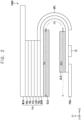
- FIG. 2 is a cross-sectional view illustrating the display device of FIG. 1 .
- FIG. 3 is a cross-sectional view illustrating a display panel included in the display device of FIG. 2 .
- the display device 1000 may include glass GLS, a display panel PNL, a bending protection layer BPL, an integrated circuit IC, and a printed circuit board PCB.
- the display device 1000 may be divided into a display area DA, a bending area BA, and a non-display area NDA.
- the display area DA may be an area parallel to a plane formed in a first direction D1 and a second direction D2 crossing the first direction D1.
- the display panel PNL may be located in the display area DA, and images may be displayed at the display area.
- the bending area BA may be adjacent to the display area DA in the second direction D2 and may be bent from the display area DA (e.g., in a direction away from a window WIN).
- the non-display area NDA may be connected to the bending area BA and overlap the display area DA when the bending area BA is bent, and the integrated circuit IC and the printed circuit board PCB may be located in the non-display area NDA. As the display device 1000 is bent in the bending area BA, a dead space of the display device 1000 may be reduced.
- the non-display area NDA may be an area at which images are not displayed.
- the glass GLS may support the display panel PNL.
- the display panel PNL may be stacked from the glass GLS in a third direction D3 perpendicular to the first and second directions D1 and D2.
- a thickness of the glass GLS may be in a range of 200 ⁇ m to 300 ⁇ m.
- materials that can be used as the glass GLS may include ultra-thin tempered glass (UTG), glass, quartz, plastic, and the like. These may be used alone or in combination with each other.
- the glass GLS may be composed of a single layer or multiple layers in combination with each other.
- the glass GLS may be removed from the bending area BA. Accordingly, the glass GLS may be prevented from being broken in the bending area BA, and the display device 1000 may be bent more smoothly without being damaged.
- the bending protection layer BPL may be located in the bending area BA on the substrate SUB.
- the bending protection layer BPL may protect the display device 1000 from stress generated when the display device 1000 is bent.
- Examples of materials that can be used as the bending protection layer BPL may include acrylic-based resins and urethane-based resins. These may be used alone or in combination with each other.
- the integrated circuit IC may be located in the non-display area NDA on the substrate SUB.
- the integrated circuit IC may correspond to the data driver DDV and may be electrically connected to the display panel PNL through the substrate SUB.
- the printed circuit board PCB may be located in the non-display area NDA on the substrate SUB.
- the controller CON may be mounted on the printed circuit board PCB, and may be electrically connected to the integrated circuit IC and the display panel PNL through the substrate SUB.
- the display panel PNL may include the substrate SUB, a transistor layer TRL, a light emitting diode layer LED, an encapsulation layer TFE, a sensing layer TSL, a polarization layer POL, and a window WIN.
- the transistor layer TRL may include a lower metal pattern BML, a buffer layer BFR, an active pattern ACT, a gate insulating layer GI, a gate electrode GAT, an interlayer insulating layer ILD, first and second connection electrodes CE1 and CE2, and a via layer VIA.
- the light emitting diode layer LED may include a pixel electrode ADE, a pixel defining layer PDL, an emission layer EL, and a common electrode CTE.
- the encapsulation layer TFE may include a first inorganic layer IL1, an organic layer OL, and a second inorganic layer IL2.
- the substrate SUB may include an organic insulating material such as plastic such as polyimide (PI) or an inorganic insulating material such as organic.
- the substrate SUB may be composed of a single layer or multiple layers in combination with each other.
- the lower metal pattern BML may be located on the substrate SUB.
- the lower metal pattern BML may be formed of a metal, an alloy, a conductive metal oxide, a transparent conductive material, or the like.
- materials that can be used as the lower metal pattern BML may include silver (Ag), an alloy containing silver, molybdenum (Mo), an alloy containing molybdenum, aluminum (Al), an alloy containing aluminum, aluminum nitride (AIN), tungsten (W), tungsten nitride (WN), copper (Cu), nickel (Ni), chromium (Cr), chromium nitride (CrN), titanium (Ti), tantalum (Ta), platinum (Pt), scandium (Sc), indium tin oxide (ITO), indium zinc oxide (IZO), and the like. These may be used alone or in combination with each other.
- the lower metal pattern BML may be formed as a single layer or as multiple layers in combination with each other.
- the buffer layer BFR may be located on the substrate SUB and may cover the lower metal pattern BML.
- the buffer layer BFR may be formed of an inorganic insulating material. Examples of materials that can be used as the inorganic insulating material may include silicon oxide, silicon nitride, and silicon oxynitride. These may be used alone or in combination with each other.
- the buffer layer BFR may prevent diffusion of metal atoms or atoms or impurities from the substrate SUB into the active pattern ACT.
- the buffer layer BFR may control a heat supply rate during a crystallization process for forming the active pattern ACT.
- the active pattern ACT may be located on the buffer layer BFR.
- the active pattern ACT may be formed of a silicon semiconductor material or an oxide semiconductor material.
- the silicon semiconductor material that can be used as the active pattern ACT may include amorphous silicon and polycrystalline silicon.
- the oxide semiconductor material that can be used as the active pattern ACT may include InGaZnO (IGZO) and InSnZnO (ITZO).
- the oxide semiconductor material may further include indium (In), gallium (Ga), tin (Sn), zirconium (Zr), vanadium (V), hafnium (Hf), cadmium (Cd), germanium (Ge), chromium (Cr), titanium (Ti), and zinc (Zn). These may be used alone or in combination with each other.
- the gate insulating layer GI may cover the active pattern ACT and may be located on the buffer layer BFR. According to some embodiments, the gate insulating layer GI may be formed of an insulating material. Examples of an insulating material that can be used as the gate insulating layer GI may include silicon oxide, silicon nitride, and silicon oxynitride. These may be used alone or in combination with each other.
- the gate electrode GAT may be located on the gate insulating layer GI.
- the gate electrode GAT may be formed of metal, alloy, conductive metal oxide, transparent conductive material, or the like.
- materials that can be used for the gate electrode GAT may include silver (Ag), an alloy containing silver, molybdenum (Mo), an alloy containing molybdenum, aluminum (Al), an alloy containing aluminum, aluminum nitride (AlN), tungsten (W), tungsten nitride (WN), copper (Cu), nickel (Ni), chromium (Cr), chromium nitride (CrN), titanium (Ti), tantalum (Ta), platinum (Pt), scandium (Sc), indium tin oxide (ITO), indium zinc oxide (IZO), and the like. These may be used alone or in combination with each other.
- the interlayer insulating layer ILD may be located on the buffer layer BFR.
- the interlayer insulating layer ILD may cover the gate electrode GAT.
- the interlayer insulating layer ILD may be formed of an insulating material. Examples of insulating materials that can be used as the interlayer insulating layer ILD may include silicon oxide, silicon nitride, and silicon oxynitride. These may be used alone or in combination with each other.
- the first and second connection electrodes CE1 and CE2 may be located on the interlayer insulating layer ILD. According to some embodiments, the first and second connection electrodes CE1 and CE2 may be formed of metal, alloy, conductive metal oxide, transparent conductive material, or the like.
- Examples of materials that may be used as the first and second connection electrodes CE1 and CE2 may include silver (Ag), an alloy containing silver, molybdenum (Mo), an alloy containing molybdenum, aluminum (Al), an alloy containing aluminum, aluminum nitride (AlN), tungsten (W), tungsten nitride (WN), copper (Cu), nickel (Ni), chromium (Cr), chromium nitride (CrN), titanium (Ti), tantalum (Ta), platinum (Pt), scandium (Sc), indium tin oxide (ITO), indium zinc oxide (IZO), and the like. These may be used alone or in combination with each other.
- the first connection electrode CE1 may contact the lower metal pattern BML and the active pattern ACT, and the second connection electrode CE2 may contact the active pattern ACT.
- the via layer VIA may cover the first and second connection electrodes CE1 and CE2 and may be located on the interlayer insulating layer ILD. According to some embodiments, the via layer VIA may be formed of an organic material. Examples of organic materials that can be used for the via layer VIA may include photoresist, polyacrylic resin, polyimide resin, and acrylic resin. These may be used alone or in combination with each other.
- the pixel electrode ADE may be located on the via layer VIA.
- the pixel electrode ADE may be formed of metal, alloy, conductive metal oxide, transparent conductive material, or the like.
- materials that can be used as the pixel electrode ADE may include silver (Ag), an alloy containing silver, molybdenum (Mo), an alloy containing molybdenum, aluminum (Al), an alloy containing aluminum, aluminum nitride (AlN), tungsten (W), tungsten nitride (WN), copper (Cu), nickel (Ni), chromium (Cr), chromium nitride (CrN), titanium (Ti), tantalum (Ta), platinum (Pt), scandium (Sc), indium tin oxide (ITO), indium zinc oxide (IZO), and the like. These may be used alone or in combination with each other.
- the pixel defining layer PDL may be located on the pixel electrode ADE and may cover an end of the pixel electrode ADE. According to some embodiments, the pixel defining layer PDL may be formed of an organic material. Examples of organic materials that can be used as the pixel defining layer PDL may include photoresist, polyacrylic resin, polyimide resin, and acrylic resin. These may be used alone or in combination with each other.
- the emission layer EL may be located on the pixel electrode ADE.
- the common electrode CTE may be located on the emission layer EL.
- the first inorganic layer IL1 may be located on the common electrode CTE. According to some embodiments, the first inorganic layer IL1 may be formed of an inorganic material. Examples of inorganic materials that may be used as the first inorganic layer IL1 may include silicon oxide, silicon nitride, and silicon oxynitride. These may be used alone or in combination with each other.
- the organic layer OL may be located on the first inorganic layer IL1.
- the organic layer OL may be formed of an organic material. Examples of organic materials that can be used as the organic layer OL may include photoresist, polyacrylic resin, polyimide resin, and acrylic resin. These may be used alone or in combination with each other.
- the second inorganic layer IL2 may be located on the organic layer OL.
- the second inorganic layer IL2 may be formed of an inorganic material.
- inorganic materials that may be used as the second inorganic layer IL2 may include silicon oxide, silicon nitride, and silicon oxynitride. These may be used alone or in combination with each other.
- the sensing layer TSL may be located on the second inorganic layer IL2. According to some embodiments, the sensing layer TSL may be a touch panel and may sense a user's touch.
- the polarization layer POL may be located on the sensing layer TSL.
- the polarization layer POL may polarize light and increase light efficiency of the emission layer EL.
- the window WIN may be located on the polarization layer POL.
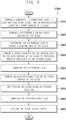
- FIG. 4 is a flowchart illustrating a method of manufacturing a display device according to some embodiments of the present invention. Embodiments according to the present invention are not limited to the number and order of operations illustrated in FIG. 4 , unless otherwise stated or implied. For example, some embodiments may include additional operations or fewer operations, and the operations may be executed in a different order without departing from the scope of embodiments according to the present invention.
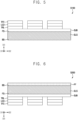
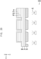
- FIGS. 5 to 15 are diagrams illustrating the method of FIG. 4 .
- the substrate SUB, the transistor layer TRL, the light emitting diode layer LED, and the encapsulation layer TFE may be sequentially formed on a front surface FS of the glass GLS (S100). Parts of the transistor layer TRL, the light emitting diode layer LED, and the encapsulation layer TFE may be spaced apart from each other. In other words, grooves may be formed between the sequentially arranged areas of the transistor layer TRL, the light emitting diode layer LED, and the encapsulation layer TFE.
- a patterning film PF may be formed on a back surface BS of the glass GLS.
- the patterning film PF may be a dry film resist (DFR), and a thickness of the dry film resist may be about 40 ⁇ m to about 50 ⁇ m.
- the bending area BA of the glass GLS may be exposed by patterning the patterning film PF (S300).
- the back surface BS corresponding to the bending area BA of the glass GLS may be exposed through the pattern of the patterning film PF.
- the bending area BA may be provided by patterning the patterning film PF, in particular by grooves GR provided in the patterning film PF and in particular in the glass GLS.
- the bending area BA may be provided by the grooves GR itself, wherein a number of grooves GR provided in the patterning film PF and in particular in the glass GLS may define the bending area BA.
- each groove GR may define a part of the bending area BA.
- abrasive particles P may be provided to the exposed glass GLS, and a groove GR overlap the bending area BA may be formed on the back surface BS of the glass GLS (S400).
- a depth of the groove GR may be about 230 ⁇ m to about 280 ⁇ m.
- the groove GR may be formed by a blast process using the abrasive particles P.
- the blast process may include a sand blast process, a micro blast process, and the like.
- the grooves GR may be corresponding to the grooves that are formed between the sequentially arranged areas of the transistor layer TRL, the light emitting diode layer LED, and the encapsulation layer TFE.
- the abrasive particles P may be chemically stable particles from the glass GLS. In other words, the abrasive particles P may not chemically react with the glass GLS.
- materials that can be used as the abrasive particles P may include alumina oxide (Al 2 O 3 ), glass beads, or silicon carbide (SiC), etc.
- An average diameter of the abrasive particles P may be about 3 ⁇ m to about 4 ⁇ m.
- the abrasive particles P may be provided from a polishing device PD including a spraying part SB.
- the spraying part SB may be a blaster. After the polishing device PD is aligned so that the spraying part SB corresponds to the bending area BA, a blasting process may be performed while the polishing device PD moves upward on the patterning film PF.
- the patterning film PF may be removed (S500).
- an acid-resistant film AF may be formed on the front surface FS of the glass GLS (S600). According to some embodiments, the acid-resistant film AF may be attached while covering the substrate SUB and the encapsulation layer TFE. In addition, a separate protective film may be further attached between the encapsulation layer TFE and the acid-resistant film AF.
- the acid-resistant film AF may protect the substrate SUB, the transistor layer TRL, the light emitting diode layer LED, and the encapsulation layer TFE from an etching solution (e.g., hydrofluoric acid solution).
- the glass GLS may be wet etched using an etching solution ECT (S700).
- the etching solution ECT may be a hydrofluoric acid solution
- the glass GLS may be isotropically etched by the hydrofluoric acid solution. Accordingly, an overall thickness of the glass GLS may be reduced, and the glass GLS overlapping the bending area BA where the groove GR is formed may be completely removed.
- the wet etching process may be performed by rotating the glass GLS at 90 degrees, but embodiments according to the present invention are not limited thereto.
- the grooves GR may become trapezoid in a cross-sectional view.
- the forming of the groove GR may be performed in a first chamber CB1.
- the etching of the glass GLS may be performed in a second chamber CB2.
- the first chamber CB1 and the second chamber CB2 may be different from each other. Accordingly, while the glass GLS is being etched in the second chamber CB2, foreign substances generated in the blasting process performed in the first chamber CB1 may be blocked from the surface of the glass GLS.
- the acid-resistant film AF may be removed (S800).
- the glass GLS may be cut in cell units along a cutting line CL (S900).
- the cutting line CL may correspond to the edges of the groove in the transistor layer TRL, the light emitting diode layer LED, and the encapsulation layer TFE and to the outer edge of the grooves GR having a trapezoid shape.
- the transistor layer TRL, the light emitting diode layer LED, and the encapsulation layer TFE may be formed on the glass GLS, the groove GR may be formed in the glass GLS through the blast process, and the glass GLS may be etched through a wet etching process.
- the glass GLS may serve as a support substrate while forming the transistor layer TRL, the light emitting diode layer LED, and the encapsulation layer TFE, and may relatively improve durability of the display device 1000.
- the etching distribution of the wet etching process may be relatively improved, and the taper angle of the glass GLS may be formed to a target angle.
- FIG. 16 is a flowchart illustrating a method of manufacturing a display device according to some embodiments of the present invention. Embodiments according to the present invention are not limited to the number and order of operations illustrated in FIG. 16 , unless otherwise stated or implied. For example, some embodiments may include additional operations or fewer operations, and the operations may be executed in a different order without departing from the scope of embodiments according to the present invention.
- FIGS. 17 to 22 are diagrams illustrating the method of FIG. 16 .
- a laser protection layer LPL, the substrate SUB, the transistor layer TRL, the light emitting diode layer LED, and the encapsulation layer TFE may be sequentially formed (S110).
- the laser protection layer LPL may be located between the glass GLS and the substrate SUB, and may protect the substrate SUB from a laser.
- a groove GR overlapping the bending area BA may be formed by irradiating a laser L to the back surface BS of the glass GLS (S210). For example, by inducing ablation of the glass GLS using thermal energy generated by the laser L, a portion of the glass GLS may be removed so that the groove GR is formed.
- the acid-resistant film AF may be formed on the front surface FS of the glass GLS (S600). According to some embodiments, the acid-resistant film AF may be attached while covering the substrate SUB and the encapsulation layer TFE. In addition, a separate protective film may be further attached between the encapsulation layer TFE and the acid-resistant film AF.
- the acid-resistant film AF may protect the substrate SUB, the transistor layer TRL, the light emitting diode layer LED, and the encapsulation layer TFE from an etching solution (e.g., hydrofluoric acid solution).
- the glass GLS may be wet etched with an etching solution ECT (S700).
- the etching solution ECT may be a hydrofluoric acid solution
- the glass GLS may be isotropically etched by the hydrofluoric acid solution. Accordingly, the overall thickness of the glass GLS may be reduced, and the glass GLS overlapping the bending area BA where the groove GR is formed may be completely removed.
- the acid-resistant film AF may be removed (S800).
- the glass GLS may be cut in cell units along the cutting line CL (S900).
- the transistor layer TRL, the light emitting diode layer LED, and the encapsulation layer (TFE) may be formed on the glass GLS, the groove GR may be formed in the glass GLS through the laser, and the glass GLS may be etched through a wet etching process.
- the glass GLS may serve as a support substrate while forming the transistor layer TRL, the light emitting diode layer LED, and the encapsulation layer TFE, and may relatively improve durability of the display device 1000.
- the groove GR is formed by irradiating a laser, chemical by-products may not be generated during the formation of the groove GR. Accordingly, the etching distribution of the wet etching process may be relatively improved, and the taper angle of the glass GLS may be formed to a target angle.
Landscapes
- Chemical & Material Sciences (AREA)
- Engineering & Computer Science (AREA)
- General Chemical & Material Sciences (AREA)
- Life Sciences & Earth Sciences (AREA)
- Chemical Kinetics & Catalysis (AREA)
- Geochemistry & Mineralogy (AREA)
- Materials Engineering (AREA)
- Organic Chemistry (AREA)
- Mechanical Engineering (AREA)
- Toxicology (AREA)
- Health & Medical Sciences (AREA)
- Ceramic Engineering (AREA)
- Electroluminescent Light Sources (AREA)
- Devices For Indicating Variable Information By Combining Individual Elements (AREA)
Abstract
Description
- Aspects of the present invention relate generally to a method of manufacturing a display device.
- A display device generally includes a display panel and at least one driver for driving the display panel, and an area in which the driver is located becomes a non-display area at which images are not displayed. Recently, display devices having a bent structure have been developed to reduce an area of the non-display area. In a display device having a bent structure, components such as a substrate may be broken in the bending area, which reduces the yield of the display device.
- The above information disclosed in this Background section is only for enhancement of understanding of the background and therefore the information discussed in this Background section does not necessarily constitute prior art.
- Aspects of the present invention relate generally to a method of manufacturing a display device. For example, aspects of some embodiments of the present invention relate to a method of manufacturing a display device having a bending area.
- The invention is defined by the independent claims. A method of manufacturing a display device according to a first aspect of the invention includes: forming a patterning film on a back surface of a glass, patterning the patterning film to expose a bending area of the glass, forming a groove overlapping the bending area on a back surface of the glass by providing abrasive particles to the exposed glass, forming an acid-resistant film on a front surface of the glass, and etching the glass.
- According to some embodiments, the groove may be formed by a blast process using the abrasive particles.
- According to some embodiments, the abrasive particles may be chemically stable particles from the glass.
- According to some embodiments, each of the abrasive particles may be alumina oxide (Al2O3).
- According to some embodiments, an average diameter of each of the abrasive particles may be about 3µm to about 4µm.
- According to some embodiments, the patterning film may be a dry film resist (DFR).
- According to some embodiments, a thickness of the dry film resist is about 40µm to about 50µm.
- According to some embodiments, the method may further include removing the patterning film, after forming the groove.
- According to some embodiments, the glass may be wet etched by hydrofluoric acid solution.
- According to some embodiments, the method may further include removing the acid-resistant film, after etching the glass.
- According to some embodiments, the method may further include forming a substrate on the front surface of the glass, forming a transistor layer on the substrate, forming a light emitting diode layer on the transistor layer, and forming an encapsulation layer on the light emitting diode layer.
- According to some embodiments, forming the groove may be performed in a first chamber, and etching the glass may be performed in a second chamber different from the first chamber.
- A method of manufacturing a display device according to a second aspect of the invention includes: forming a groove overlapping a bending area by irradiating a laser to a back surface of a glass, forming an acid-resistant film on a front surface of the glass, and etching the glass.
- According to some embodiments, the glass may be wet etched by hydrofluoric acid solution.
- According to some embodiments, the method may further include removing the acid-resistant film, after etching the glass.
- According to some embodiments, the method may further include forming a laser protection layer on the front surface of the glass, forming a substrate on the laser protection layer, forming a transistor layer on the substrate, forming a light emitting diode layer on the transistor layer, and forming an encapsulation layer on the light emitting diode layer, before irradiating the laser.
- Therefore, in the method of manufacturing a display device according to some embodiments of the present invention, a transistor layer, a light emitting diode layer, and an encapsulation layer may be formed on glass, a groove may be formed in a bending area of the glass through a blast process, and a glass may be entirely etched through a wet etching process. The glass may serve as a support substrate while forming a transistor layer, a light emitting diode layer, and an encapsulation layer, and may relatively improve durability of a display device. In addition, as the grooves are formed through the blast process, chemical by-products may not be generated during groove formation. Accordingly, the etching distribution of the wet etching process may be relatively improved, and the taper angle of the glass may be formed to a target angle.
- The accompanying drawings, which are included to provide a further understanding of the inventive concept and are incorporated in and constitute a part of this specification, illustrate embodiments of the inventive concept together with the description.
-
FIG. 1 is a block diagram illustrating a display device according to some embodiments of the present invention. -
FIG. 2 is a cross-sectional view illustrating the display device ofFIG. 1 according to some embodiments of the present invention. -
FIG. 3 is a cross-sectional view illustrating a display panel included in the display device ofFIG. 2 according to some embodiments of the present invention. -
FIG. 4 is a flowchart illustrating a method of manufacturing a display device according to some embodiments of the present invention. -
FIGS. 5 to 15 are diagrams illustrating the method ofFIG. 4 according to some embodiments of the present invention. -
FIG. 16 is a flowchart illustrating a method of manufacturing a display device according to some embodiments of the present invention. -
FIGS. 17 to 22 are diagrams illustrating the method ofFIG. 16 according to some embodiments of the present invention. - Aspects of illustrative, non-limiting embodiments will be more-clearly understood from the following detailed description in conjunction with the accompanying drawings.
-
FIG. 1 is a block diagram illustrating a display device according to some embodiments of the present invention. - Referring to
FIG. 1 , adisplay device 1000 according to some embodiments of the present invention may include a display part (or display panel) DP, a data driver DDV, a gate driver GDV, and a controller CON. - The display part DP may include at least one pixel PX. The pixel PX may emit light, and the display part DP may display images. For example, the pixel PX may emit light corresponding to a data voltage DATA in response to a gate signal GS. Although
FIG. 1 illustrates a single pixel PX, as a person having ordinary skill in the art would appreciate, the display part DP may include any suitable number of pixels PX according to the design and size of the display part DP. - The data driver DDV may generate the data voltage DATA based on an output image data ODAT and a data control signal DCTRL. For example, the data driver DDV may generate the data voltage DATA corresponding to the output image data ODAT and may output the data voltage DATA in response to the data control signal DCTRL. The data control signal DCTRL may include an output data enable signal, a horizontal start signal, and a load signal.
- The gate driver GDV may generate the gate signal GS based on a gate control signal GCTRL. For example, the gate control signal GCTRL may include a vertical start signal and a clock signal. In response to the gate signal GS, the transistor of the pixel PX may be turned on or off, and the data voltage DATA may be written into the pixel PX.
- The controller CON (e.g., a timing controller T-CON) may receive input image data IDAT and a control signal CTRL from an external host processor (e.g., GPU). For example, the input image data IDAT may be RGB data including red image data, green image data, and blue image data. The control signal CTRL may include a vertical synchronization signal, a horizontal synchronization signal, an input data enable signal, a master clock signal, and the like. The controller CON may generate the gate control signal GCTRL, the data control signal DCTRL, and the output image data ODAT based on the input image data IDAT and the control signal CTRL.
-
FIG. 2 is a cross-sectional view illustrating the display device ofFIG. 1 .FIG. 3 is a cross-sectional view illustrating a display panel included in the display device ofFIG. 2 . - Referring to
FIG. 2 , thedisplay device 1000 may include glass GLS, a display panel PNL, a bending protection layer BPL, an integrated circuit IC, and a printed circuit board PCB. - According to some embodiments, the
display device 1000 may be divided into a display area DA, a bending area BA, and a non-display area NDA. - The display area DA may be an area parallel to a plane formed in a first direction D1 and a second direction D2 crossing the first direction D1. The display panel PNL may be located in the display area DA, and images may be displayed at the display area.
- The bending area BA may be adjacent to the display area DA in the second direction D2 and may be bent from the display area DA (e.g., in a direction away from a window WIN). The non-display area NDA may be connected to the bending area BA and overlap the display area DA when the bending area BA is bent, and the integrated circuit IC and the printed circuit board PCB may be located in the non-display area NDA. As the
display device 1000 is bent in the bending area BA, a dead space of thedisplay device 1000 may be reduced. The non-display area NDA may be an area at which images are not displayed. - The glass GLS may support the display panel PNL. For example, the display panel PNL may be stacked from the glass GLS in a third direction D3 perpendicular to the first and second directions D1 and D2. According to some embodiments, a thickness of the glass GLS may be in a range of 200 µm to 300 µm. Examples of materials that can be used as the glass GLS may include ultra-thin tempered glass (UTG), glass, quartz, plastic, and the like. These may be used alone or in combination with each other. In addition, the glass GLS may be composed of a single layer or multiple layers in combination with each other.
- According to some embodiments, the glass GLS may be removed from the bending area BA. Accordingly, the glass GLS may be prevented from being broken in the bending area BA, and the
display device 1000 may be bent more smoothly without being damaged. - The bending protection layer BPL may be located in the bending area BA on the substrate SUB. The bending protection layer BPL may protect the
display device 1000 from stress generated when thedisplay device 1000 is bent. Examples of materials that can be used as the bending protection layer BPL may include acrylic-based resins and urethane-based resins. These may be used alone or in combination with each other. - The integrated circuit IC may be located in the non-display area NDA on the substrate SUB. The integrated circuit IC may correspond to the data driver DDV and may be electrically connected to the display panel PNL through the substrate SUB.
- The printed circuit board PCB may be located in the non-display area NDA on the substrate SUB. The controller CON may be mounted on the printed circuit board PCB, and may be electrically connected to the integrated circuit IC and the display panel PNL through the substrate SUB.
- Referring to
FIG. 3 , the display panel PNL may include the substrate SUB, a transistor layer TRL, a light emitting diode layer LED, an encapsulation layer TFE, a sensing layer TSL, a polarization layer POL, and a window WIN. - The transistor layer TRL may include a lower metal pattern BML, a buffer layer BFR, an active pattern ACT, a gate insulating layer GI, a gate electrode GAT, an interlayer insulating layer ILD, first and second connection electrodes CE1 and CE2, and a via layer VIA. The light emitting diode layer LED may include a pixel electrode ADE, a pixel defining layer PDL, an emission layer EL, and a common electrode CTE. The encapsulation layer TFE may include a first inorganic layer IL1, an organic layer OL, and a second inorganic layer IL2.
- The substrate SUB may include an organic insulating material such as plastic such as polyimide (PI) or an inorganic insulating material such as organic. In addition, the substrate SUB may be composed of a single layer or multiple layers in combination with each other.
- The lower metal pattern BML may be located on the substrate SUB. According to some embodiments, the lower metal pattern BML may be formed of a metal, an alloy, a conductive metal oxide, a transparent conductive material, or the like. Examples of materials that can be used as the lower metal pattern BML may include silver (Ag), an alloy containing silver, molybdenum (Mo), an alloy containing molybdenum, aluminum (Al), an alloy containing aluminum, aluminum nitride (AIN), tungsten (W), tungsten nitride (WN), copper (Cu), nickel (Ni), chromium (Cr), chromium nitride (CrN), titanium (Ti), tantalum (Ta), platinum (Pt), scandium (Sc), indium tin oxide (ITO), indium zinc oxide (IZO), and the like. These may be used alone or in combination with each other. In addition, the lower metal pattern BML may be formed as a single layer or as multiple layers in combination with each other.
- The buffer layer BFR may be located on the substrate SUB and may cover the lower metal pattern BML. According to some embodiments, the buffer layer BFR may be formed of an inorganic insulating material. Examples of materials that can be used as the inorganic insulating material may include silicon oxide, silicon nitride, and silicon oxynitride. These may be used alone or in combination with each other. The buffer layer BFR may prevent diffusion of metal atoms or atoms or impurities from the substrate SUB into the active pattern ACT. In addition, the buffer layer BFR may control a heat supply rate during a crystallization process for forming the active pattern ACT.
- The active pattern ACT may be located on the buffer layer BFR. According to some embodiments, the active pattern ACT may be formed of a silicon semiconductor material or an oxide semiconductor material. Examples of the silicon semiconductor material that can be used as the active pattern ACT may include amorphous silicon and polycrystalline silicon. Examples of the oxide semiconductor material that can be used as the active pattern ACT may include InGaZnO (IGZO) and InSnZnO (ITZO). In addition, the oxide semiconductor material may further include indium (In), gallium (Ga), tin (Sn), zirconium (Zr), vanadium (V), hafnium (Hf), cadmium (Cd), germanium (Ge), chromium (Cr), titanium (Ti), and zinc (Zn). These may be used alone or in combination with each other.
- The gate insulating layer GI may cover the active pattern ACT and may be located on the buffer layer BFR. According to some embodiments, the gate insulating layer GI may be formed of an insulating material. Examples of an insulating material that can be used as the gate insulating layer GI may include silicon oxide, silicon nitride, and silicon oxynitride. These may be used alone or in combination with each other.
- The gate electrode GAT may be located on the gate insulating layer GI. According to some embodiments, the gate electrode GAT may be formed of metal, alloy, conductive metal oxide, transparent conductive material, or the like. Examples of materials that can be used for the gate electrode GAT may include silver (Ag), an alloy containing silver, molybdenum (Mo), an alloy containing molybdenum, aluminum (Al), an alloy containing aluminum, aluminum nitride (AlN), tungsten (W), tungsten nitride (WN), copper (Cu), nickel (Ni), chromium (Cr), chromium nitride (CrN), titanium (Ti), tantalum (Ta), platinum (Pt), scandium (Sc), indium tin oxide (ITO), indium zinc oxide (IZO), and the like. These may be used alone or in combination with each other.
- The interlayer insulating layer ILD may be located on the buffer layer BFR. The interlayer insulating layer ILD may cover the gate electrode GAT. According to some embodiments, the interlayer insulating layer ILD may be formed of an insulating material. Examples of insulating materials that can be used as the interlayer insulating layer ILD may include silicon oxide, silicon nitride, and silicon oxynitride. These may be used alone or in combination with each other.
- The first and second connection electrodes CE1 and CE2 may be located on the interlayer insulating layer ILD. According to some embodiments, the first and second connection electrodes CE1 and CE2 may be formed of metal, alloy, conductive metal oxide, transparent conductive material, or the like. Examples of materials that may be used as the first and second connection electrodes CE1 and CE2 may include silver (Ag), an alloy containing silver, molybdenum (Mo), an alloy containing molybdenum, aluminum (Al), an alloy containing aluminum, aluminum nitride (AlN), tungsten (W), tungsten nitride (WN), copper (Cu), nickel (Ni), chromium (Cr), chromium nitride (CrN), titanium (Ti), tantalum (Ta), platinum (Pt), scandium (Sc), indium tin oxide (ITO), indium zinc oxide (IZO), and the like. These may be used alone or in combination with each other.
- The first connection electrode CE1 may contact the lower metal pattern BML and the active pattern ACT, and the second connection electrode CE2 may contact the active pattern ACT.
- The via layer VIA may cover the first and second connection electrodes CE1 and CE2 and may be located on the interlayer insulating layer ILD. According to some embodiments, the via layer VIA may be formed of an organic material. Examples of organic materials that can be used for the via layer VIA may include photoresist, polyacrylic resin, polyimide resin, and acrylic resin. These may be used alone or in combination with each other.
- The pixel electrode ADE may be located on the via layer VIA. According to some embodiments, the pixel electrode ADE may be formed of metal, alloy, conductive metal oxide, transparent conductive material, or the like. Examples of materials that can be used as the pixel electrode ADE may include silver (Ag), an alloy containing silver, molybdenum (Mo), an alloy containing molybdenum, aluminum (Al), an alloy containing aluminum, aluminum nitride (AlN), tungsten (W), tungsten nitride (WN), copper (Cu), nickel (Ni), chromium (Cr), chromium nitride (CrN), titanium (Ti), tantalum (Ta), platinum (Pt), scandium (Sc), indium tin oxide (ITO), indium zinc oxide (IZO), and the like. These may be used alone or in combination with each other.
- The pixel defining layer PDL may be located on the pixel electrode ADE and may cover an end of the pixel electrode ADE. According to some embodiments, the pixel defining layer PDL may be formed of an organic material. Examples of organic materials that can be used as the pixel defining layer PDL may include photoresist, polyacrylic resin, polyimide resin, and acrylic resin. These may be used alone or in combination with each other.
- The emission layer EL may be located on the pixel electrode ADE. The common electrode CTE may be located on the emission layer EL.
- The first inorganic layer IL1 may be located on the common electrode CTE. According to some embodiments, the first inorganic layer IL1 may be formed of an inorganic material. Examples of inorganic materials that may be used as the first inorganic layer IL1 may include silicon oxide, silicon nitride, and silicon oxynitride. These may be used alone or in combination with each other.
- The organic layer OL may be located on the first inorganic layer IL1. According to some embodiments, the organic layer OL may be formed of an organic material. Examples of organic materials that can be used as the organic layer OL may include photoresist, polyacrylic resin, polyimide resin, and acrylic resin. These may be used alone or in combination with each other.
- The second inorganic layer IL2 may be located on the organic layer OL. According to some embodiments, the second inorganic layer IL2 may be formed of an inorganic material. Examples of inorganic materials that may be used as the second inorganic layer IL2 may include silicon oxide, silicon nitride, and silicon oxynitride. These may be used alone or in combination with each other.
- The sensing layer TSL may be located on the second inorganic layer IL2. According to some embodiments, the sensing layer TSL may be a touch panel and may sense a user's touch. The polarization layer POL may be located on the sensing layer TSL. The polarization layer POL may polarize light and increase light efficiency of the emission layer EL. The window WIN may be located on the polarization layer POL.
-
FIG. 4 is a flowchart illustrating a method of manufacturing a display device according to some embodiments of the present invention. Embodiments according to the present invention are not limited to the number and order of operations illustrated inFIG. 4 , unless otherwise stated or implied. For example, some embodiments may include additional operations or fewer operations, and the operations may be executed in a different order without departing from the scope of embodiments according to the present invention.FIGS. 5 to 15 are diagrams illustrating the method ofFIG. 4 . - Referring to
FIGS. 4 and5 , in a method (S1000) of manufacturing of the display device according to some embodiments of the present invention, the substrate SUB, the transistor layer TRL, the light emitting diode layer LED, and the encapsulation layer TFE may be sequentially formed on a front surface FS of the glass GLS (S100). Parts of the transistor layer TRL, the light emitting diode layer LED, and the encapsulation layer TFE may be spaced apart from each other. In other words, grooves may be formed between the sequentially arranged areas of the transistor layer TRL, the light emitting diode layer LED, and the encapsulation layer TFE. - Referring to
FIGS. 4 and6 , a patterning film PF may be formed on a back surface BS of the glass GLS. According to some embodiments, the patterning film PF may be a dry film resist (DFR), and a thickness of the dry film resist may be about 40 µm to about 50 µm. - Referring to
FIGS. 4 ,7 , and8 , the bending area BA of the glass GLS may be exposed by patterning the patterning film PF (S300). In other words, the back surface BS corresponding to the bending area BA of the glass GLS may be exposed through the pattern of the patterning film PF. According to an embodiment, the bending area BA may be provided by patterning the patterning film PF, in particular by grooves GR provided in the patterning film PF and in particular in the glass GLS. Thus, the bending area BA may be provided by the grooves GR itself, wherein a number of grooves GR provided in the patterning film PF and in particular in the glass GLS may define the bending area BA. In other words, each groove GR may define a part of the bending area BA. - Referring to
FIGS. 4 ,9 , and10 , abrasive particles P may be provided to the exposed glass GLS, and a groove GR overlap the bending area BA may be formed on the back surface BS of the glass GLS (S400). For example, a depth of the groove GR may be about 230 µm to about 280 µm. - According to some embodiments, the groove GR may be formed by a blast process using the abrasive particles P. The blast process may include a sand blast process, a micro blast process, and the like. The grooves GR may be corresponding to the grooves that are formed between the sequentially arranged areas of the transistor layer TRL, the light emitting diode layer LED, and the encapsulation layer TFE.
- The abrasive particles P may be chemically stable particles from the glass GLS. In other words, the abrasive particles P may not chemically react with the glass GLS. For example, materials that can be used as the abrasive particles P may include alumina oxide (Al2O3), glass beads, or silicon carbide (SiC), etc. An average diameter of the abrasive particles P may be about 3µm to about 4µm.
- According to some embodiments, the abrasive particles P may be provided from a polishing device PD including a spraying part SB. For example, the spraying part SB may be a blaster. After the polishing device PD is aligned so that the spraying part SB corresponds to the bending area BA, a blasting process may be performed while the polishing device PD moves upward on the patterning film PF.
- Referring to
FIGS. 4 and11 , the patterning film PF may be removed (S500). - Referring to
FIGS. 4 and12 , an acid-resistant film AF may be formed on the front surface FS of the glass GLS (S600). According to some embodiments, the acid-resistant film AF may be attached while covering the substrate SUB and the encapsulation layer TFE. In addition, a separate protective film may be further attached between the encapsulation layer TFE and the acid-resistant film AF. The acid-resistant film AF may protect the substrate SUB, the transistor layer TRL, the light emitting diode layer LED, and the encapsulation layer TFE from an etching solution (e.g., hydrofluoric acid solution). - Referring to
FIGS. 4 and13 , the glass GLS may be wet etched using an etching solution ECT (S700). According to some embodiments, the etching solution ECT may be a hydrofluoric acid solution, and the glass GLS may be isotropically etched by the hydrofluoric acid solution. Accordingly, an overall thickness of the glass GLS may be reduced, and the glass GLS overlapping the bending area BA where the groove GR is formed may be completely removed. - According to some embodiments, as shown in
FIG. 13 , the wet etching process may be performed by rotating the glass GLS at 90 degrees, but embodiments according to the present invention are not limited thereto. Thus, the grooves GR may become trapezoid in a cross-sectional view. - According to some embodiments, as shown in
FIGS. 9 and10 , the forming of the groove GR may be performed in a first chamber CB1. In addition, as shown inFIG. 13 , the etching of the glass GLS may be performed in a second chamber CB2. In this case, the first chamber CB1 and the second chamber CB2 may be different from each other. Accordingly, while the glass GLS is being etched in the second chamber CB2, foreign substances generated in the blasting process performed in the first chamber CB1 may be blocked from the surface of the glass GLS. - Referring to
FIGS. 4 and14 , after the wet etching process is performed, the acid-resistant film AF may be removed (S800). - Referring to
FIGS. 4 and15 , the glass GLS may be cut in cell units along a cutting line CL (S900). The cutting line CL may correspond to the edges of the groove in the transistor layer TRL, the light emitting diode layer LED, and the encapsulation layer TFE and to the outer edge of the grooves GR having a trapezoid shape. - In the method (S1000) of manufacturing a display device according to some embodiments of the present invention, the transistor layer TRL, the light emitting diode layer LED, and the encapsulation layer TFE may be formed on the glass GLS, the groove GR may be formed in the glass GLS through the blast process, and the glass GLS may be etched through a wet etching process. The glass GLS may serve as a support substrate while forming the transistor layer TRL, the light emitting diode layer LED, and the encapsulation layer TFE, and may relatively improve durability of the
display device 1000. In addition, as the grooves GR are formed through the blasting process, chemical by-products may not be generated during the formation of the grooves GR. Accordingly, the etching distribution of the wet etching process may be relatively improved, and the taper angle of the glass GLS may be formed to a target angle. -
FIG. 16 is a flowchart illustrating a method of manufacturing a display device according to some embodiments of the present invention. Embodiments according to the present invention are not limited to the number and order of operations illustrated inFIG. 16 , unless otherwise stated or implied. For example, some embodiments may include additional operations or fewer operations, and the operations may be executed in a different order without departing from the scope of embodiments according to the present invention.FIGS. 17 to 22 are diagrams illustrating the method ofFIG. 16 . - Referring to
FIGS. 16 and17 , in the method (S2000) of manufacturing a display device according to some embodiments of the present invention, a laser protection layer LPL, the substrate SUB, the transistor layer TRL, the light emitting diode layer LED, and the encapsulation layer TFE may be sequentially formed (S110). The laser protection layer LPL may be located between the glass GLS and the substrate SUB, and may protect the substrate SUB from a laser. - Referring to
FIGS. 16 and18 , a groove GR overlapping the bending area BA may be formed by irradiating a laser L to the back surface BS of the glass GLS (S210). For example, by inducing ablation of the glass GLS using thermal energy generated by the laser L, a portion of the glass GLS may be removed so that the groove GR is formed. - Referring to
FIGS. 16 and19 , the acid-resistant film AF may be formed on the front surface FS of the glass GLS (S600). According to some embodiments, the acid-resistant film AF may be attached while covering the substrate SUB and the encapsulation layer TFE. In addition, a separate protective film may be further attached between the encapsulation layer TFE and the acid-resistant film AF. The acid-resistant film AF may protect the substrate SUB, the transistor layer TRL, the light emitting diode layer LED, and the encapsulation layer TFE from an etching solution (e.g., hydrofluoric acid solution). - Referring to
FIGS. 16 and20 , the glass GLS may be wet etched with an etching solution ECT (S700). According to some embodiments, the etching solution ECT may be a hydrofluoric acid solution, and the glass GLS may be isotropically etched by the hydrofluoric acid solution. Accordingly, the overall thickness of the glass GLS may be reduced, and the glass GLS overlapping the bending area BA where the groove GR is formed may be completely removed. - Referring to
FIGS. 16 and21 , after the wet etching process is performed, the acid-resistant film AF may be removed (S800). - Referring to
FIGS. 16 and22 , the glass GLS may be cut in cell units along the cutting line CL (S900). - In the method (S2000) of manufacturing a display device according to some embodiments of the present invention, the transistor layer TRL, the light emitting diode layer LED, and the encapsulation layer (TFE) may be formed on the glass GLS, the groove GR may be formed in the glass GLS through the laser, and the glass GLS may be etched through a wet etching process. The glass GLS may serve as a support substrate while forming the transistor layer TRL, the light emitting diode layer LED, and the encapsulation layer TFE, and may relatively improve durability of the
display device 1000. In addition, as the groove GR is formed by irradiating a laser, chemical by-products may not be generated during the formation of the groove GR. Accordingly, the etching distribution of the wet etching process may be relatively improved, and the taper angle of the glass GLS may be formed to a target angle. - Although aspects of some embodiments and implementations have been described herein, other embodiments and modifications will be apparent from this description. Accordingly, embodiments according to the present invention are not limited to the specific disclosed embodiments, but rather to the broader scope of the appended claims, and various obvious modifications as would be apparent to a person of ordinary skill in the art.
Claims (16)
- A method of manufacturing a display device (1000), the method comprising:forming a patterning film (PF) on a back surface (BS) of a glass (GLS);patterning the patterning film (PF) to expose a bending area (BA) of the glass (GLS);forming a groove (GR) overlapping the bending area (BA) on a back surface (BS) of the glass (GLS) by providing abrasive particles (P) to the exposed glass (GLS);forming an acid-resistant film (AF) on a front surface (FS) of the glass (GLS); andetching the glass (GLS).
- The method of claim 1, wherein the groove (GR) is formed by a blast process using the abrasive particles (P).
- The method of claim 1 or 2, wherein the abrasive particles (P) are chemically stable particles from the glass (GLS).
- The method of at least one of claims 1 to 3, wherein each of the abrasive particles (P) is alumina oxide (Al2O3).
- The method of at least one of claims 1 to 3, wherein an average diameter of each of the abrasive particles (P) is in a range of 3 µm to 4 µm.
- The method of at least one of claims 1 to 5, wherein the patterning film (PF) is a dry film resist.
- The method of claim 6, wherein a thickness of the dry film resist is in a range of 40 µm to 50 µm.
- The method of at least one of claims 1 to 7, further comprising:
removing the patterning film (PF), after forming the groove (GR). - The method of at least one of claims 1 to 8, wherein the glass (GLS) is wet etched by hydrofluoric acid solution.
- The method of at least one of claims 1 to 9, further comprising:
removing the acid-resistant film (AF), after etching the glass (GLS). - The method of at least one of claims 1 to 10, further comprising:forming a substrate (SUB) on the front surface (FS) of the glass (GLS);forming a transistor layer (TRL) on the substrate (SUB);forming a light emitting diode layer (LED) on the transistor layer (TRL); andforming an encapsulation layer (TFE) on the light emitting diode layer (LED).
- The method of at least one of claims 1 to 11, wherein forming the groove (GR) is performed in a first chamber (CB1), and
etching the glass (GLS) is performed in a second chamber (CB2) different from the first chamber (CB1). - A method of manufacturing a display device (1000), the method comprising:forming a groove (GR) overlapping a bending area (BA) by irradiating a laser to a back surface (BS) of a glass (GLS);forming an acid-resistant film (AF) on a front surface (FS) of the glass (GLS); andetching the glass (GLS).
- The method of claim 13, wherein the glass (GLS) is wet etched by a hydrofluoric acid solution.
- The method of claim 13 or 14, further comprising:
removing the acid-resistant film (AF), after etching the glass (GLS). - The method of at least one of claims 13 to 15, further comprising:forming a laser protection layer (LPL) on the front surface (FS) of the glass (GLS);forming a substrate (SUB) on the laser protection layer (LPL);forming a transistor layer (TRL) on the substrate (SUB);forming a light emitting diode layer (LED) on the transistor layer (TRL); andforming an encapsulation layer (TFE) on the light emitting diode layer (LED), before irradiating the laser.
Applications Claiming Priority (1)
| Application Number | Priority Date | Filing Date | Title |
|---|---|---|---|
| KR1020230054253A KR20240157825A (en) | 2023-04-25 | 2023-04-25 | Method of manufacturing display device |
Publications (1)
| Publication Number | Publication Date |
|---|---|
| EP4461709A1 true EP4461709A1 (en) | 2024-11-13 |
Family
ID=90482144
Family Applications (1)
| Application Number | Title | Priority Date | Filing Date |
|---|---|---|---|
| EP24166599.1A Pending EP4461709A1 (en) | 2023-04-25 | 2024-03-27 | Method of manufacturing display device |
Country Status (4)
| Country | Link |
|---|---|
| US (1) | US20240360031A1 (en) |
| EP (1) | EP4461709A1 (en) |
| KR (1) | KR20240157825A (en) |
| CN (1) | CN118841429A (en) |
Citations (2)
| Publication number | Priority date | Publication date | Assignee | Title |
|---|---|---|---|---|
| KR20140058725A (en) * | 2012-11-05 | 2014-05-15 | 동우 화인켐 주식회사 | Method of manufacturing glass substrate for display device |
| EP4291006A2 (en) * | 2022-05-16 | 2023-12-13 | Samsung Display Co., Ltd. | Display device, electronic device including the same, and method of manufacturing the display device |
Family Cites Families (5)
| Publication number | Priority date | Publication date | Assignee | Title |
|---|---|---|---|---|
| TW419442B (en) * | 1996-12-18 | 2001-01-21 | Koninkl Philips Electronics Nv | Method of post-etching a mechanically treated substrate |
| US20150225283A1 (en) * | 2014-02-10 | 2015-08-13 | Hony Glass Technology Co., Ltd. | Glass Substrate and Method of Manufacturing the Same |
| JP2017111987A (en) * | 2015-12-17 | 2017-06-22 | 株式会社Nsc | Method for manufacturing glass substrate for light guide plate |
| KR102749972B1 (en) * | 2019-04-11 | 2025-01-03 | 삼성디스플레이 주식회사 | Display device |
| KR102146730B1 (en) * | 2019-12-23 | 2020-08-24 | (주)유티아이 | Flexible Cover Window |
-
2023
- 2023-04-25 KR KR1020230054253A patent/KR20240157825A/en active Pending
-
2024
- 2024-02-15 US US18/443,043 patent/US20240360031A1/en active Pending
- 2024-03-27 EP EP24166599.1A patent/EP4461709A1/en active Pending
- 2024-04-25 CN CN202410506902.6A patent/CN118841429A/en active Pending
Patent Citations (2)
| Publication number | Priority date | Publication date | Assignee | Title |
|---|---|---|---|---|
| KR20140058725A (en) * | 2012-11-05 | 2014-05-15 | 동우 화인켐 주식회사 | Method of manufacturing glass substrate for display device |
| EP4291006A2 (en) * | 2022-05-16 | 2023-12-13 | Samsung Display Co., Ltd. | Display device, electronic device including the same, and method of manufacturing the display device |
Also Published As
| Publication number | Publication date |
|---|---|
| KR20240157825A (en) | 2024-11-04 |
| CN118841429A (en) | 2024-10-25 |
| US20240360031A1 (en) | 2024-10-31 |
Similar Documents
| Publication | Publication Date | Title |
|---|---|---|
| US11164932B2 (en) | Backplane for display device and method of manufacturing the same | |
| CN111596783B (en) | Display apparatus | |
| KR20240046860A (en) | Organic light emitting display device | |
| KR101932126B1 (en) | Touch-type organic light-emitting diode display device | |
| CN106206645B (en) | Organic light-emitting display device and method of manufacturing the same | |
| KR102553981B1 (en) | Backplane for display device and method of manufacturing the same | |
| EP3902008B1 (en) | Light emitting display device and manufacturing method thereof | |
| KR102653947B1 (en) | Display device and method of fabricating the same | |
| KR102320186B1 (en) | Organic light emitting display device and method of fabricating the same | |
| KR20150037159A (en) | Flexible display device and manufacturing method thereof | |
| KR20160054867A (en) | Flexible organic light emitting display device and method for manufacturing the same | |
| US20180321763A1 (en) | Touch substrate and fabrication method thereof, and display device | |
| CN110364553A (en) | Organic LED display device | |
| US12082435B2 (en) | Display device and method of manufacturing display device | |
| US20230023524A1 (en) | Display device and method of manufacturing the display device | |
| KR102426498B1 (en) | Array Substrate For Touch Display Device And Method Of Fabricating The Same | |
| CN109935728A (en) | Organic light-emitting display device | |
| US20230028400A1 (en) | Display device | |
| US20250054932A1 (en) | Method of manufacturing display device | |
| US20240360031A1 (en) | Method of manufacturing display device | |
| US20230282790A1 (en) | Display device and method of manufacturing the same | |
| US12588340B2 (en) | Display device | |
| KR102959372B1 (en) | Display device and method of manufacturing the same | |
| KR20250122977A (en) | Method of manufacturing display device | |
| CN121057472A (en) | Display modules, display panels and their manufacturing methods, and display devices. |
Legal Events
| Date | Code | Title | Description |
|---|---|---|---|
| PUAI | Public reference made under article 153(3) epc to a published international application that has entered the european phase |
Free format text: ORIGINAL CODE: 0009012 |
|
| STAA | Information on the status of an ep patent application or granted ep patent |
Free format text: STATUS: THE APPLICATION HAS BEEN PUBLISHED |
|
| AK | Designated contracting states |
Kind code of ref document: A1 Designated state(s): AL AT BE BG CH CY CZ DE DK EE ES FI FR GB GR HR HU IE IS IT LI LT LU LV MC ME MK MT NL NO PL PT RO RS SE SI SK SM TR |
|
| STAA | Information on the status of an ep patent application or granted ep patent |
Free format text: STATUS: REQUEST FOR EXAMINATION WAS MADE |
|
| 17P | Request for examination filed |
Effective date: 20250424 |
|
| P01 | Opt-out of the competence of the unified patent court (upc) registered |
Free format text: CASE NUMBER: UPC_APP_0007433_4461709/2026 Effective date: 20260226 |