EP4459978A1 - Diskrete grafikrahmeninterpolationsschaltung, verfahren und vorrichtung, chip, elektronische vorrichtung und medium - Google Patents
Diskrete grafikrahmeninterpolationsschaltung, verfahren und vorrichtung, chip, elektronische vorrichtung und medium Download PDFInfo
- Publication number
- EP4459978A1 EP4459978A1 EP22914929.9A EP22914929A EP4459978A1 EP 4459978 A1 EP4459978 A1 EP 4459978A1 EP 22914929 A EP22914929 A EP 22914929A EP 4459978 A1 EP4459978 A1 EP 4459978A1
- Authority
- EP
- European Patent Office
- Prior art keywords
- data
- chip
- independent display
- frame rate
- electronic device
- Prior art date
- Legal status (The legal status is an assumption and is not a legal conclusion. Google has not performed a legal analysis and makes no representation as to the accuracy of the status listed.)
- Pending
Links
Images


Classifications
-
- G—PHYSICS
- G06—COMPUTING OR CALCULATING; COUNTING
- G06F—ELECTRIC DIGITAL DATA PROCESSING
- G06F3/00—Input arrangements for transferring data to be processed into a form capable of being handled by the computer; Output arrangements for transferring data from processing unit to output unit, e.g. interface arrangements
- G06F3/14—Digital output to display device ; Cooperation and interconnection of the display device with other functional units
-
- G—PHYSICS
- G09—EDUCATION; CRYPTOGRAPHY; DISPLAY; ADVERTISING; SEALS
- G09G—ARRANGEMENTS OR CIRCUITS FOR CONTROL OF INDICATING DEVICES USING STATIC MEANS TO PRESENT VARIABLE INFORMATION
- G09G3/00—Control arrangements or circuits, of interest only in connection with visual indicators other than cathode-ray tubes
- G09G3/20—Control arrangements or circuits, of interest only in connection with visual indicators other than cathode-ray tubes for presentation of an assembly of a number of characters, e.g. a page, by composing the assembly by combination of individual elements arranged in a matrix no fixed position being assigned to or needed to be assigned to the individual characters or partial characters
- G09G3/34—Control arrangements or circuits, of interest only in connection with visual indicators other than cathode-ray tubes for presentation of an assembly of a number of characters, e.g. a page, by composing the assembly by combination of individual elements arranged in a matrix no fixed position being assigned to or needed to be assigned to the individual characters or partial characters by control of light from an independent source
- G09G3/36—Control arrangements or circuits, of interest only in connection with visual indicators other than cathode-ray tubes for presentation of an assembly of a number of characters, e.g. a page, by composing the assembly by combination of individual elements arranged in a matrix no fixed position being assigned to or needed to be assigned to the individual characters or partial characters by control of light from an independent source using liquid crystals
-
- G—PHYSICS
- G09—EDUCATION; CRYPTOGRAPHY; DISPLAY; ADVERTISING; SEALS
- G09G—ARRANGEMENTS OR CIRCUITS FOR CONTROL OF INDICATING DEVICES USING STATIC MEANS TO PRESENT VARIABLE INFORMATION
- G09G5/00—Control arrangements or circuits for visual indicators common to cathode-ray tube indicators and other visual indicators
- G09G5/003—Details of a display terminal, the details relating to the control arrangement of the display terminal and to the interfaces thereto
- G09G5/005—Adapting incoming signals to the display format of the display terminal
-
- H—ELECTRICITY
- H04—ELECTRIC COMMUNICATION TECHNIQUE
- H04N—PICTORIAL COMMUNICATION, e.g. TELEVISION
- H04N5/00—Details of television systems
- H04N5/04—Synchronising
-
- H—ELECTRICITY
- H04—ELECTRIC COMMUNICATION TECHNIQUE
- H04N—PICTORIAL COMMUNICATION, e.g. TELEVISION
- H04N7/00—Television systems
- H04N7/01—Conversion of standards, e.g. involving analogue television standards or digital television standards processed at pixel level
-
- H—ELECTRICITY
- H04—ELECTRIC COMMUNICATION TECHNIQUE
- H04N—PICTORIAL COMMUNICATION, e.g. TELEVISION
- H04N7/00—Television systems
- H04N7/01—Conversion of standards, e.g. involving analogue television standards or digital television standards processed at pixel level
- H04N7/0127—Conversion of standards, e.g. involving analogue television standards or digital television standards processed at pixel level by changing the field or frame frequency of the incoming video signal, e.g. frame rate converter
-
- G—PHYSICS
- G09—EDUCATION; CRYPTOGRAPHY; DISPLAY; ADVERTISING; SEALS
- G09G—ARRANGEMENTS OR CIRCUITS FOR CONTROL OF INDICATING DEVICES USING STATIC MEANS TO PRESENT VARIABLE INFORMATION
- G09G2330/00—Aspects of power supply; Aspects of display protection and defect management
- G09G2330/02—Details of power systems and of start or stop of display operation
- G09G2330/021—Power management, e.g. power saving
-
- G—PHYSICS
- G09—EDUCATION; CRYPTOGRAPHY; DISPLAY; ADVERTISING; SEALS
- G09G—ARRANGEMENTS OR CIRCUITS FOR CONTROL OF INDICATING DEVICES USING STATIC MEANS TO PRESENT VARIABLE INFORMATION
- G09G2340/00—Aspects of display data processing
- G09G2340/04—Changes in size, position or resolution of an image
- G09G2340/0407—Resolution change, inclusive of the use of different resolutions for different screen areas
- G09G2340/0435—Change or adaptation of the frame rate of the video stream
-
- G—PHYSICS
- G09—EDUCATION; CRYPTOGRAPHY; DISPLAY; ADVERTISING; SEALS
- G09G—ARRANGEMENTS OR CIRCUITS FOR CONTROL OF INDICATING DEVICES USING STATIC MEANS TO PRESENT VARIABLE INFORMATION
- G09G2370/00—Aspects of data communication
-
- G—PHYSICS
- G09—EDUCATION; CRYPTOGRAPHY; DISPLAY; ADVERTISING; SEALS
- G09G—ARRANGEMENTS OR CIRCUITS FOR CONTROL OF INDICATING DEVICES USING STATIC MEANS TO PRESENT VARIABLE INFORMATION
- G09G5/00—Control arrangements or circuits for visual indicators common to cathode-ray tube indicators and other visual indicators
- G09G5/12—Synchronisation between the display unit and other units, e.g. other display units, video-disc players
-
- G—PHYSICS
- G09—EDUCATION; CRYPTOGRAPHY; DISPLAY; ADVERTISING; SEALS
- G09G—ARRANGEMENTS OR CIRCUITS FOR CONTROL OF INDICATING DEVICES USING STATIC MEANS TO PRESENT VARIABLE INFORMATION
- G09G5/00—Control arrangements or circuits for visual indicators common to cathode-ray tube indicators and other visual indicators
- G09G5/18—Timing circuits for raster scan displays
Definitions
- This application pertains to the field of communications technologies, and in particular, to an independent display frame interpolation circuit, method, and apparatus, a chip, an electronic device, and a medium.
- some electronic devices can support the display of videos, games, and other images with high frame rate.
- the display frame rate of the electronic device is affected due to the high power consumption of the electronic device, which leads to the low fluency of the image displayed on the electronic device.
- Embodiments of this application aim to provide an independent display frame interpolation circuit, method, and apparatus, a chip, an electronic device, and a medium.
- an embodiment of this application provides an independent display frame interpolation circuit, where the independent display frame interpolation circuit includes a System-on-a-Chip and an independent display chip.
- the System-on-a-Chip is configured to: generate first data based on first content to be displayed, and send the first data to the independent display chip in a case that a target display frame rate synchronization (TE) signal sent by the independent display chip is received, where a frame rate of the first data is smaller than a frame rate of the first content; and the independent display chip is configured to perform frame interpolation processing on the first data to obtain second data, and a frame rate of the second data is greater than or equal to the frame rate of the first content.
- TE target display frame rate synchronization
- an embodiment of this application provides an independent display frame interpolation method, and the independent display frame interpolation method includes: generating first data based on first content to be displayed on the electronic device through a System-on-a-Chip in the electronic device, where a frame rate of the first data is smaller than a frame rate of the first content; in a case that the System-on-a-Chip receives a target display frame rate synchronization (TE) signal sent by an independent display chip in the electronic device, sending the first data to the independent display chip through the System-on-a-Chip; and performing frame interpolation processing on the first data through the independent display chip to obtain second data, where a frame rate of the second data is greater than or equal to the frame rate of the first content.
- TE target display frame rate synchronization
- an embodiment of this application provides an independent display frame interpolation apparatus, where the independent display frame interpolation apparatus includes a generating module, a sending module, and a processing module.
- the generating module is configured to generate first data based on first content to be displayed on the electronic device through a System-on-a-Chip in the electronic device, where a frame rate of the first data is smaller than a frame rate of the first content.
- the sending module is configured to: in a case that the System-on-a-Chip receives a target display frame rate synchronization (TE) signal sent by an independent display chip in the electronic device, send the first data to the independent display chip through the System-on-a-Chip.
- the processing module is configured to perform frame interpolation processing on the first data through the independent display chip to obtain second data, where a frame rate of the second data is greater than or equal to the frame rate of the first content.
- TE target display frame rate synchronization
- an embodiment of this application provides a System-on-a-Chip, where the System-on-a-Chip includes a processor and a communications interface, the communications interface is coupled to the processor, the processor is configured to generate first data based on first content to be displayed on an electronic device, where a frame rate of the first data is smaller than a frame rate of the first content, and the communications interface is configured to: in a case that a target display frame rate synchronization (TE) signal sent by an independent display chip in the electronic device is received, send the first data to the independent display chip.
- TE target display frame rate synchronization
- an embodiment of this application provides an independent display chip, where the independent display chip includes a processor and a communications interface, the communications interface is coupled to the processor, the communications interface is configured to: send a target display frame rate synchronization (TE) signal to a System-on-a-Chip in an electronic device, and receive first data sent by the System-on-a-Chip, where the first data is data generated by the System-on-a-Chip based on first content to be displayed on the electronic device, a frame rate of the first data is smaller than a frame rate of the first content; and the processor is configured to perform frame interpolation processing on the first data to obtain second data, and a frame rate of the second data is greater than or equal to the frame rate of the first content.
- TE target display frame rate synchronization
- an embodiment of this application provides an electronic device, where the electronic device includes the independent display frame interpolation circuit according to the first aspect, or includes the System-on-a-Chip according to the fourth aspect and the independent display chip according to the fifth aspect.
- an embodiment of this application provides an electronic device.
- the electronic device includes a processor and a memory.
- the processor stores a program or an instruction executable on the processor.
- steps of the method according to the second aspect are implemented by the electronic device.
- an embodiment of this application provides a readable storage medium.
- the readable storage medium stores a program or an instruction, and when the program or the instruction is executed by a processor, steps of the method according to the second aspect are implemented by the electronic device.
- an embodiment of this application provides a computer program product.
- the program product is stored in a storage medium, and the program product is executed by at least one processor to implement the method according to the second aspect by the electronic device.
- the System-on-a-Chip can generate the first data based on the first content to be displayed, and the frame rate of the first data is smaller than that of the first content. Then, in a case that the System-on-a-Chip receives the target TE signal sent by the independent display chip, the System-on-a-Chip can send the first data to the independent display chip, so that the independent display chip performs frame interpolation processing on the first data to obtain second data, and a frame rate of the second data is greater than or equal to that of the first content.
- the frame rate of the first data generated by the System-on-a-Chip is smaller than that of the first content to be displayed, that is, the output frame rate of the System-on-a-Chip is reduced.
- the independent display chip can perform frame interpolation processing on the first data to obtain the second data, so as to improve or maintain the frame rate of the content to be displayed on the electronic device.
- the output frame rate of the System-on-a-Chip is reduced, and the problem that high power consumption of the System-on-a-Chip affects a frame interpolation function of the independent display chip can be avoided, thereby improving the fluency of the image displayed on the electronic device.
- first”, “second”, and the like in this specification and claims of this application are used to distinguish between similar objects instead of describing a specific order or sequence. It should be understood that data used in such a way are interchangeable in proper circumstances, so that the embodiments of this application can be implemented in an order other than the order illustrated or described herein.
- Objects classified by "first”, “second”, and the like are usually of a same type, and the number of objects is not limited. For example, there may be one or more first objects.
- "and/or" represents at least one of connected objects, and a character “/" generally represents an "or” relationship between associated objects.
- some electronic devices can support the display of videos, games, and other images with high frame rate.
- the display frame rate of the electronic device is affected due to the high power consumption of the electronic device, which leads to the low fluency of the image displayed on the electronic device.
- an output frame rate of the System-on-a-Chip (System-on-a-Chip, SoC) can be reduced, and then the frame is interpolated to a target frame rate (greater than or equal to a frame rate of currently displayed content) through an independent display chip, so that the power consumption of the SoC can be reduced while a frame rate of the content displayed on the electronic device is improved or maintained, so as to stabilize the output frame rate of the SoC, thereby improving the fluency of the image displayed on the electronic device.
- a display frame rate of a liquid crystal display module is 90 fps
- a frame rate of a program source that is, a frame rate of content to be displayed on the electronic device
- the LCM sends a 90-Hz TE signal to the independent display chip for frame synchronization.
- the independent display chip adjusts the TE signal to be in 45 Hz and sends the TE signal to the SoC, and in addition, the SoC processes generated frame data from 60 fps to 45 fps and transmits the frame data to the independent display chip, so that the independent display chip interpolates frame on the 45-fps frame data to be 90-fps frame data and transmits the frame data to the LCM.
- the LCM displays content corresponding to the 90-fps frame data. In this way, while improving the frame rate of the content to be displayed on the electronic device, the power consumption of the SoC is reduced to stabilize the output frame rate of the SoC, thereby improving the fluency of the image displayed on the electronic device.
- the display frame rate of the LCM is 90 fps
- a frame rate of a program source that is, a frame rate of content to be displayed on the electronic device
- 60 fps the LCM sends a 90-Hz TE signal to the independent display chip for frame synchronization.
- the independent display chip adjusts the TE signal to be in 30 Hz and sends the TE signal to the SoC, and in addition, the SoC processes generated frame data from 60 fps to 30 fps and transmits the frame data to the independent display chip (or the independent display chip adjusts the TE signal to be in 45 Hz and sends the TE signal to the SoC, and the SoC processes generated frame data from 60 fps to 45 fps and transmits the frame data to the independent display chip, which can be adjusted according to the needs of power consumption and effect), so that the independent display chip interpolates frame on the 30-fps frame data to be 60-fps frame data and transmits the frame data to the LCM.
- the LCM displays content corresponding to the 60-fps frame data.
- the power consumption of the SoC is reduced to stabilize the output frame rate of the SoC, thereby improving the fluency of the image displayed on the electronic device.
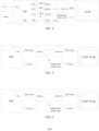
- FIG. 3 is a schematic diagram of a structure of an independent display frame interpolation circuit according to an embodiment of this application.
- the independent display frame interpolation circuit provided in this embodiment of this application may include a System-on-a-Chip and an independent display chip.
- the System-on-a-Chip is configured to: generate first data based on first content to be displayed, and send the first data to the independent display chip in a case that a target TE signal sent by the independent display chip is received, where a frame rate of the first data is smaller than a frame rate of the first content.
- the independent display chip is configured to perform frame interpolation processing on the first data to obtain second data, and a frame rate of the second data is greater than or equal to the frame rate of the first content.
- the independent display chip can bring display enhancement effects such as a higher frame rate, a higher resolution, a higher color saturation and contrast.
- a high frame rate for example, 120/90 Hz
- the actually displayed content does not achieve a real high frame rate, and only relies on a graphics processing unit (Graphics Processing Unit, GPU) or a display driving integrated circuit for simple image repetition, and the actual experience is still at a low frame rate.
- the independent display chip can calculate a motion feature of the image by using data of two frames before and after, and simulate and generate a middle image to realize dynamic frame compensation, so as to enable the content displayed on the electronic device to realize real high frame rate.
- FIG. 4 is a schematic diagram of an architecture of an independent display chip.
- the independent display chip has two display serial interface (Display Serial Interface, DSI), and data transmission is realized through a mobile industry processor interface (Mobile Industry Processor Interface, MIPI) protocol, which can work in a double-channel MIPI mode and a single-channel MIPI mode.
- MIPI Mobile Industry Processor Interface
- the display content can be divided into a user interface (User Interface, UI) layer and a video (video) layer.
- UI User Interface
- video video
- the UI layer and the video layer are separately transmitted to the independent display chip through the DSI interface, and processed by various functional modules in the independent display chip (such as frame interpolation, super resolution, noise reduction, color enhancement, and the like) to synthesize frame data.
- the display content is transmitted to the liquid crystal display module (Liquid Crystal Display Module, LCM) through a display serial interface-transmit (DSI-Transmit, DSI-Tx) 0.
- the display content can be sent to the independent display chip via the DSI 0 by the SoC after synthesizing the frame data, so that the independent display chip can be transmitted to the liquid crystal display module after being processed correspondingly.
- a photographing scenario content photographed by a camera in the electronic device is transmitted to the SoC through a camera serial interface (Camera Serial Interface, CSI) 0, and the SoC transmits photographed content to the independent display chip through the DSI interface.
- the processed content is transmitted to the SoC and the liquid crystal display module through the CSI Tx0 and DSI Tx0 interfaces respectively.
- the SoC can store the processed content, and the liquid crystal display module can preview and display the processed content in real time.
- FIG. 5 is a signal interaction diagram when the electronic device does not enable an independent display frame interpolation function.
- a frame rate of the display is 90 fps.
- the LCM sends a 90-Hz TE signal to the independent display chip for frame synchronization, and the independent display chip also synchronously generates a 90-Hz TE signal and sends the TE signal to the SoC.
- the program source is only 60 fps
- the GPU will generate 60-fps frame data which is transmitted to the independent display chip, and then the independent display chip directly transmits the frame data to the display. In this case, real content displayed on the display is only 60 fps, which cannot reach 90 fps of the display.
- FIG. 6 is a signal interaction diagram when the electronic device enables an independent display frame interpolation function.
- a frame rate of the display is 90 fps.
- the LCM sends a 90-Hz TE signal to the independent display chip for frame synchronization, and the independent display chip synchronously generates a 60-Hz TE signal and sends the TE signal to the SoC.
- the SoC will generate 60-fps frame data which is transmitted to the independent display chip, and then the independent display chip interpolates frame on 60 fps to be 90 fps, and transmits the frame data to the display. In this case, the content displayed on the display can reach real 90 fps.
- the first content may be a video image, a game image, or the like. This may be specifically determined according to an actual use requirement, and is not limited in this embodiment of this application.
- the System-on-a-Chip may perform frame loss processing on the first content, or may perform any other possible processing on the first content to obtain the first data.
- the System-on-a-Chip is specifically configured to perform frame loss processing on the first content based on a preset frame rate, to obtain first data at the preset frame rate.
- the preset frame rate is smaller than a frame rate of the first content.
- the preset frame rate can be the default of the electronic device or preset by the user. This may be specifically determined according to an actual use requirement, and is not limited in this embodiment of this application.
- the System-on-a-Chip will lose 1-fps data every time when the System-on-a-Chip processes 3-fps data. The lost frame of data does not need to be processed, and the data actually processed by the System-on-a-Chip is 45 fps.
- the System-on-a-Chip will lose 1-fps data every time when the System-on-a-Chip processes 1-fps data.
- the lost frame of data does not need to be processed, and the data actually processed by the System-on-a-Chip is 30 fps.
- the System-on-a-Chip can perform frame loss processing on the first content based on the preset frame rate, to obtain the first data at the preset frame rate, that is, reduce the output frame rate of the System-on-a-Chip, so that the power consumption of the System-on-a-Chip can be reduced to stabilize the output frame rate of the System-on-a-Chip, and the problem that high power consumption of the System-on-a-Chip affects the independent display frame interpolation function can be avoided, thereby improving the fluency of the image displayed on the electronic device.
- the target TE signal may be one TE signal or include a plurality of TE signals. This may be specifically determined according to an actual use requirement, and is not limited in this embodiment of this application.
- the System-on-a-Chip is further configured to send a first instruction to the independent display chip, where the first instruction includes a preset frame rate.
- the independent display chip is further configured to: generate the target TE signal, and send the target TE signal to the System-on-a-Chip, where a frequency value of the target TE signal is equal to a value of the preset frame rate.
- the System-on-a-Chip can send a first instruction including a preset frame rate to the independent display chip, so that the independent display chip can generate a TE signal with a frequency value equal to the value of the preset frame rate, and send the TE signal to the System-on-a-Chip.
- the electronic device reduces the power consumption of the System-on-a-Chip by reducing the output frame rate of the System-on-a-Chip, and stabilizes the output frame rate of the System-on-a-Chip, thereby improving the fluency of the image displayed on the electronic device.
- the first instruction further includes a target frame rate.
- the independent display chip is specifically configured to perform frame interpolation processing on the first data by using the target frame rate, to obtain the second data.
- the System-on-a-Chip sends the first instruction including the preset frame rate and the target frame rate to the independent display chip, so that the independent display chip enters a mode in which "interpolating frame on the preset frame rate to be the target frame rate", and when the independent display chip receives the first data, the independent display chip can perform frame interpolation processing on the first data to obtain second data at the target frame rate.
- the independent display chip can perform other processing (such as super resolution, noise reduction, color enhancement, and the like) on the first data while performing frame interpolation processing, and finally obtain the second data.
- other processing such as super resolution, noise reduction, color enhancement, and the like
- the frame rate of the second data may be preset by the user, or may be the default of the electronic device. This may be specifically determined according to an actual use requirement, and is not limited in this embodiment of this application.
- the frame rate of the second data may be greater than that of the first content in a case of a high frame rate mode; and the frame rate of the second data may be equal to the frame rate of the first content in a case of a power saving mode.
- the independent display chip can perform frame interpolation processing on the first data with a frame rate smaller than that of the first content, to obtain the second data with a frame rate greater than or equal to that of the first content, so as to improve or maintain the frame rate of the content displayed on the electronic device while reducing the power consumption of the System-on-a-Chip, thereby improving the fluency of the image displayed on the electronic device.
- the target TE signal includes a plurality of TE signals.
- the System-on-a-Chip is specifically configured to send one frame of data in the first data to the independent display chip every time when the System-on-a-Chip receives one TE signal, so as to send a plurality of frames of data in the first data to the independent display chip.
- the TE signal is one TE signal in the plurality of TE signals.
- the System-on-a-Chip can send a first frame of data in the first data to the independent display chip when the System-on-a-Chip receives a first TE signal, the System-on-a-Chip can send a second frame of data in the first data to the independent display chip when the System-on-a-Chip receives a second TE signal, ..., and so on, until the System-on-a-Chip sends all frames of data in the first data to the independent display chip.
- the independent display chip every time when receiving one frame of data in the first data, the independent display chip processes the frame of data, and after the processing of the frame of data is completed, the independent display chip sends one TE signal to the System-on-a-Chip, so as to process all frames of data in the first data. It can be understood that each TE signal corresponds to one frame of data in the first data.
- the independent display chip can send one TE signal to the System-on-a-Chip, and then the System-on-a-Chip sends one frame of data to the independent display chip.
- the System-on-a-Chip sends one frame of data in the first data to the independent display chip
- the System-on-a-Chip sends all frames of data in the first data to the independent display chip, thus avoiding a case that the independent display chip receives a next frame of data before completing processing of one frame of data, thus ensuring the timing of data processing performed by the System-on-a-Chip and the independent display chip.
- the independent display frame interpolation circuit further includes a display unit.
- the independent display chip is further configured to: in a case that a first TE signal sent by a display unit is received, send second data to the display unit, where a frequency value of the first TE signal is greater than or equal to a value of the frame rate of the second data.
- the display unit is configured to display second content based on the second data.
- the first TE signal may be one TE signal or include a plurality of TE signals. This may be specifically determined according to an actual use requirement, and is not limited in this embodiment of this application.
- the independent display chip every time when the independent display chip receives one TE signal in the first TE signal, the independent display chip sends one frame of data in the second data to the display unit, so as to send a plurality of frames of data in the second data to the display unit.
- each TE signal in the first TE signal corresponds to one frame of data in the second data.
- the independent display chip can send a plurality of frames of data to the display unit in turn, and then the display unit displays content corresponding to each frame of data in turn, so that the display unit displays the second content.
- the display unit displays content corresponding to the frame of data.
- the frequency value of the first TE signal is greater than the value of the frame rate of the second data
- the display unit can display content corresponding to frame data received by the display unit for the last time.
- the display unit displays content corresponding to frame data received by the display unit for the last time when the target frame data is not received by the display unit.
- the display unit can receive the second data sent by the independent display chip and display second content corresponding to the second data, that is, the content with a high frame rate is displayed or the content displayed by the display unit is maintained. In this way, the problem that high power consumption of the System-on-a-Chip affects the frame interpolation function of the independent display chip is avoided, thereby improving the fluency of the image displayed on the electronic device.
- FIG. 7 is a flowchart of an independent display frame interpolation method according to an embodiment of this application, and the method can be applied to an electronic device.
- the independent display frame interpolation method provided in this embodiment of this application may include the following step 201 to step 203.
- Step 201 The electronic device generates first data based on first content to be displayed on the electronic device through a System-on-a-Chip in the electronic device.
- the frame rate of the first data is smaller than a frame rate of the first content.
- the electronic device can generate the first data based on the first content (such as video images or game images) to be displayed on the electronic device through the System-on-a-Chip, and the frame rate of the first data is smaller than that of the first content, that is, the output frame rate of the System-on-a-Chip is reduced.
- first content such as video images or game images
- the electronic device sends the first data to the independent display chip through the System-on-a-Chip, so that the independent display chip performs frame interpolation processing on the first data to obtain second data, and a frame rate of the second data is greater than or equal to that of the first content, that is, a frame rate of the content displayed on the electronic device is improved or maintained.
- the electronic device may perform frame loss processing on the first content through the System-on-a-Chip, or may also perform any other possible processing on the first content through the System-on-a-Chip, to obtain the first data.
- step 201 can be specifically implemented by performing the following step 201a.
- Step 201a The electronic device performs frame loss processing on the first content based on a preset frame rate through the System-on-a-Chip, to obtain first data at the preset frame rate.
- the preset frame rate is smaller than a frame rate of the first content.
- the electronic device can perform frame loss processing on the first content based on the preset frame rate through the System-on-a-Chip, to obtain the first data at the preset frame rate, that is, reduce the output frame rate of the System-on-a-Chip, so that the power consumption of the System-on-a-Chip can be reduced to stabilize the output frame rate of the System-on-a-Chip, and the problem that high power consumption of the System-on-a-Chip affects the independent display frame interpolation function can be avoided, thereby improving the fluency of the image displayed on the electronic device.
- Step 202 In a case that the System-on-a-Chip receives a target TE signal sent by an independent display chip in the electronic device, the electronic device sends the first data to the independent display chip through the System-on-a-Chip.
- the independent display chip in the electronic device may send the target TE signal to the System-on-a-Chip, so that the electronic device sends the first data to the independent display chip through the System-on-a-Chip.
- the target TE signal may be one TE signal or include a plurality of TE signals. This may be specifically determined according to an actual use requirement, and is not limited in this embodiment of this application.
- the target TE signal includes a plurality of TE signals.
- the foregoing step 202 may be specifically implemented by the following step 202a.
- Step 202a The electronic device sends one frame of data in the first data to the independent display chip through the System-on-a-Chip every time when the System-on-a-Chip receives one TE signal, so as to send a plurality of frames of data in the first data to the independent display chip through the System-on-a-Chip.
- the electronic device sends one TE signal to the System-on-a-Chip through the independent display chip, and then the electronic device sends one frame of data to the independent display chip through the System-on-a-Chip.
- the electronic device sends one frame of data in the first data to the independent display chip through the System-on-a-Chip, and finally sends all frames of data in the first data to the independent display chip through the System-on-a-Chip, thus avoiding a case that the independent display chip receives a next frame of data before completing processing of one frame of data, thus ensuring the timing of data processing performed by the System-on-a-Chip and the independent display chip.
- Step 203 The electronic device performs frame interpolation processing on the first data through the independent display chip to obtain second data.
- the frame rate of the second data is greater than or equal to a frame rate of the first content.
- the independent display frame interpolation method provided in this embodiment of this application further includes the following step 301 and step 302.
- Step 301 The electronic device sends a first instruction to the independent display chip through the System-on-a-Chip.
- the first instruction includes a preset frame rate.
- Step 302. The electronic device generates a target TE signal through the independent display chip, and sends the target TE signal to the System-on-a-Chip through the independent display chip.
- the frequency value of the target TE signal is equal to the value of the preset frame rate.
- the electronic device can send a first instruction including a preset frame rate to the independent display chip through the System-on-a-Chip, so that the electronic device can generate a TE signal with a frequency value equal to the value of the preset frame rate through the independent display chip, and send the TE signal to the System-on-a-Chip through the independent display chip.
- the electronic device can send data at the preset frame rate to the independent display chip through the System-on-a-Chip, and because the preset frame rate is smaller than the frame rate of the first content, that is, the electronic device reduces the power consumption of the System-on-a-Chip by reducing the output frame rate of the System-on-a-Chip, and stabilizes the output frame rate of the System-on-a-Chip, thereby improving the fluency of the image displayed on the electronic device.
- the first instruction further includes a target frame rate.
- the foregoing step 203 may be specifically implemented by the following step 203a.
- Step 203a The electronic device performs frame interpolation processing on the first data through the independent display chip by using the target frame rate, to obtain the second data.
- the electronic device can perform frame interpolation processing on the first data with a frame rate smaller than that of the first content through the independent display chip, to obtain the second data with a frame rate greater than or equal to that of the first content.
- the electronic device can improve or maintain the frame rate of the content displayed on the electronic device while reducing the power consumption of the System-on-a-Chip, thereby improving the fluency of the image displayed on the electronic device.
- the electronic device can generate the first data based on the first content to be displayed on the electronic device through the System-on-a-Chip, and the frame rate of the first data is smaller than that of the first content. Then, in a case that the System-on-a-Chip receives the target TE signal sent by the independent display chip in the electronic device, the electronic device sends the first data to the independent display chip through the System-on-a-Chip, so that the independent display chip performs frame interpolation processing on the first data to obtain second data, and a frame rate of the second data is greater than or equal to that of the first content.
- the frame rate of the first data generated by the System-on-a-Chip is smaller than that of the first content to be displayed on the electronic device, that is, the output frame rate of the System-on-a-Chip is reduced.
- the independent display chip can perform frame interpolation processing on the first data to obtain the second data, so as to improve or maintain the frame rate of the content to be displayed on the electronic device.
- the output frame rate of the System-on-a-Chip is reduced, and the problem that high power consumption of the System-on-a-Chip affects the independent display frame interpolation function can be avoided, thereby improving the fluency of the image displayed on the electronic device.
- the independent display frame interpolation method provided in this embodiment of this application further includes the following step 401 and step 402.
- Step 401 In a case that the independent display chip receives a first TE signal sent by a display unit in the electronic device, the electronic device sends second data to the display chip through the independent display chip.
- a frequency value of the first TE signal is greater than or equal to a value of the frame rate of the second data.
- Step 402. The electronic device displays second content based on the second data through the display unit.
- the electronic device can receive the second data sent by the independent display chip through the display unit and display second content corresponding to the second data, that is, the content with a high frame rate is displayed or the content displayed by the display unit is maintained through the display unit.
- the problem that high power consumption of the System-on-a-Chip affects the frame interpolation function of the independent display chip is avoided, thereby improving the fluency of the image displayed on the electronic device.
- the independent display frame interpolation method provided in this embodiment of this application may be executed by an independent display frame interpolation apparatus.
- an example in which the independent display frame interpolation apparatus performs the independent display frame interpolation method is used to describe the independent display frame interpolation apparatus provided in this embodiment of this application.
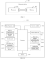
- FIG. 8 is a schematic diagram of a possible structure of an independent display frame interpolation apparatus according to an embodiment of this application.
- the independent display frame interpolation apparatus 70 may include a generating module 71, a sending module 72, and a processing module 73.
- the generating module 71 is configured to generate first data based on first content to be displayed on the electronic device through a System-on-a-Chip in the electronic device, where a frame rate of the first data is smaller than a frame rate of the first content.
- the sending module 72 is configured to: in a case that the System-on-a-Chip receives a target display frame rate synchronization (TE) signal sent by an independent display chip in the electronic device, send the first data to the independent display chip through the System-on-a-Chip.
- the processing module 73 is configured to perform frame interpolation processing on the first data through the independent display chip to obtain second data, where a frame rate of the second data is greater than or equal to the frame rate of the first content.
- TE target display frame rate synchronization
- the frame rate of the first data generated by the System-on-a-Chip is smaller than that of the first content displayed on the independent display frame interpolation apparatus, that is, the output frame rate of the System-on-a-Chip is reduced.
- the independent display chip can perform frame interpolation processing on the first data to obtain the second data, so as to improve or maintain the frame rate of the content to be displayed on the independent display frame interpolation apparatus.
- the generating module 71 is specifically configured to perform frame loss processing on the first content based on a preset frame rate through the System-on-a-Chip, to obtain first data at the preset frame rate.
- the sending module 72 is further configured to: in a case that the System-on-a-Chip receives a target TE signal sent by an independent display chip in the electronic device, before sending the first data to the independent display chip through the System-on-a-Chip, send a first instruction to the independent display chip through the System-on-a-Chip, where the first instruction includes a preset frame rate.
- the generating module 71 is further configured to generate a target TE signal through the independent display chip.
- the sending module 72 is further configured to send the target TE signal to the System-on-a-Chip through the independent display chip, where a frequency value of the target TE signal is equal to a value of the preset frame rate.
- the first instruction further includes a target frame rate.
- the processing module 73 is specifically configured to perform frame interpolation processing on the first data through the independent display chip by using the target frame rate, to obtain the second data.
- the target TE signal includes a plurality of TE signals.
- the sending module 72 is specifically configured to send one frame of data in the first data to the independent display chip through the System-on-a-Chip every time when the System-on-a-Chip receives one TE signal, so as to send a plurality of frames of data in the first data to the independent display chip through the System-on-a-Chip.
- the independent display frame interpolation apparatus 70 further includes a display module.
- the sending module 72 is further configured to: after performing frame interpolation processing on the first data through the independent display chip to obtain second data, in a case that the independent display chip receives a first TE signal sent by a display unit in the electronic device, send the second data to the display unit through the independent display chip, where a frequency value of the first TE signal is greater than or equal to a value of the frame rate of the second data.
- the display module is configured to display second content based on the second data through the display unit.
- the independent display frame interpolation apparatus in this embodiment of this application may be an electronic device, or may be a component such as a circuit or a chip in the electronic device.
- the electronic device may be a terminal, or another device other than the terminal.
- the electronic device may be a mobile phone, a tablet computer, a notebook computer, a palmtop computer, an in-vehicle electronic device, a mobile Internet device (Mobile Internet Device, MID), an augmented reality (augmented reality, AR)/virtual reality (virtual reality, VR) device, a robot, a wearable device, an ultra-mobile personal computer (ultra-mobile personal computer, UMPC), a netbook, a personal digital assistant (personal digital assistant, PDA), or the like. This is not specifically limited in this embodiment of this application.
- the independent display frame interpolation apparatus in this embodiment of this application may be an apparatus with an operating system.
- the operating system may be an Android (Android) operating system, an iOS operating system, or another possible operating system. This is not specifically limited in the embodiments of this application.
- the independent display frame interpolation apparatus provided in this embodiment of this application can implement the processes of the foregoing method embodiments, and a same technical effect can be achieved. To avoid repetition, details are not described herein again.
- An embodiment of this application further provides a System-on-a-Chip, where the System-on-a-Chip includes a processor and a communications interface, the communications interface is coupled to the processor, the processor is configured to generate first data based on first content to be displayed on an electronic device, where a frame rate of the first data is smaller than a frame rate of the first content, and the communications interface is configured to: in a case that a target TE signal sent by an independent display chip in the electronic device is received, send the first data to the independent display chip.
- the processor is specifically configured to perform frame loss processing on the first content based on a preset frame rate, to obtain first data at the preset frame rate.
- the communications interface is further configured to send a first instruction to the independent display chip, where the first instruction includes a preset frame rate.
- the communications interface is further configured to receive the target TE signal sent by the independent display chip, where a frequency value of the target TE signal is equal to a value of the preset frame rate.
- the target TE signal includes a plurality of TE signals.
- the communications interface is specifically configured to send one frame of data in the first data to the independent display chip every time when receiving one TE signal, so as to send a plurality of frames of data in the first data to the independent display chip.
- the System-on-a-Chip provided in this embodiment of this application can implement the processes implemented by the System-on-a-Chip in the method embodiment, and a same technical effect can be achieved. To avoid repetition, details are not described herein again.
- An embodiment of this application further provides an independent display chip, where the independent display chip includes a processor and a communications interface, the communications interface is coupled to the processor, the communications interface is configured to: send a target TE signal to a System-on-a-Chip in an electronic device, and receive first data sent by the System-on-a-Chip, where the first data is data generated by the System-on-a-Chip based on first content to be displayed on the electronic device, a frame rate of the first data is smaller than a frame rate of the first content; and the processor is configured to perform frame interpolation processing on the first data to obtain second data, and a frame rate of the second data is greater than or equal to the frame rate of the first content.
- the independent display chip includes a processor and a communications interface
- the communications interface is coupled to the processor, the communications interface is configured to: send a target TE signal to a System-on-a-Chip in an electronic device, and receive first data sent by the System-on-a-Chip, where the first data is data
- the communications interface is further configured to receive a first instruction sent by the System-on-a-Chip, where the first instruction includes a preset frame rate.
- the processor is further configured to generate a target TE signal.
- the communications interface is further configured to send the target TE signal to the System-on-a-Chip, where a frequency value of the target TE signal is equal to a value of the preset frame rate.
- the first instruction further includes a target frame rate.
- the processor is specifically configured to perform frame interpolation processing on the first data by using the target frame rate, to obtain the second data.
- the target TE signal includes a plurality of TE signals.
- the communications interface is specifically configured to receive one frame of data in the first data sent by the System-on-a-Chip every time when sending one TE signal, so as to receive a plurality of frames of data in the first data sent by the System-on-a-Chip.
- the communications interface is further configured to: in a case that a first TE signal sent by a display unit in the electronic device is received, send the second data to the display unit, where a frequency value of the first TE signal is greater than or equal to a value of the frame rate of the second data.
- the independent display chip provided in this embodiment of this application can implement the processes implemented by the independent display chip in the method embodiments, and a same technical effect can be achieved. To avoid repetition, details are not described herein again.
- an embodiment of this application further provides an electronic device 800, including a processor 801, a memory 802, and a program or an instruction stored in the memory 802 and executable on the processor 801, where the program or the instruction is executed by the processor 801 to implement the steps of the foregoing independent display frame interpolation method embodiment, and a same technical effect can be achieved. To avoid repetition, details are not described herein again.
- the electronic device in this embodiment of this application includes the foregoing mobile electronic device and the foregoing non-mobile electronic device.
- FIG. 10 is a schematic diagram of a hardware structure of an electronic device according to an embodiment of this application.
- An electronic device 1000 includes but is not limited to components such as a radio frequency unit 1001, a network module 1002, an audio output unit 1003, an input unit 1004, a sensor 1005, a display unit 1006, a user input unit 1007, an interface unit 1008, a memory 1009, and a processor 1010.
- the electronic device 1000 may further include a power supply (such as a battery) that supplies power to each component.
- the power supply may be logically connected to the processor 1010 by using a power supply management system, to implement functions such as charging and discharging management, and power consumption management by using the power supply management system.
- the structure of the electronic device shown in FIG. 10 does not constitute a limitation on the electronic device.
- the electronic device may include components more or fewer than those shown in the diagram, a combination of some components, or different component arrangements. Details are not described herein.
- the processor 1010 is configured to: generate first data based on first content to be displayed on the electronic device through a System-on-a-Chip in the electronic device, where a frame rate of the first data is smaller than a frame rate of the first content; in a case that the System-on-a-Chip receives a target TE signal sent by an independent display chip in the electronic device, send the first data to the independent display chip through the System-on-a-Chip; and perform frame interpolation processing on the first data through the independent display chip to obtain second data, where a frame rate of the second data is greater than or equal to the frame rate of the first content.
- An embodiment of this application provides an electronic device, where the frame rate of the first data generated by the System-on-a-Chip is smaller than that of the first content displayed on the electronic device, that is, the output frame rate of the System-on-a-Chip is reduced. Then, the independent display chip can perform frame interpolation processing on the first data to obtain the second data, so as to improve or maintain the frame rate of the content displayed on the electronic device. In this way, the output frame rate of the System-on-a-Chip is reduced, and the problem that high power consumption of the System-on-a-Chip affects the independent display frame interpolation function can be avoided, thereby improving the fluency of the image displayed on the electronic device.
- the processor 1010 is specifically configured to perform frame loss processing on the first content based on a preset frame rate through the System-on-a-Chip, to obtain first data at the preset frame rate.
- the processor 1010 is further configured to: in a case that the System-on-a-Chip receives a target TE signal sent by an independent display chip in the electronic device, before sending the first data to the independent display chip through the System-on-a-Chip, send a first instruction to the independent display chip through the System-on-a-Chip, where the first instruction includes a preset frame rate.
- the processor 1010 is further configured to: generate the target TE signal through the independent display chip, and send the target TE signal to the System-on-a-Chip through the independent display chip, where a frequency value of the target TE signal is equal to a value of the preset frame rate.
- the first instruction further includes a target frame rate.
- the processor 1010 is specifically configured to perform frame interpolation processing on the first data through the independent display chip by using the target frame rate, to obtain the second data.
- the target TE signal includes a plurality of TE signals.
- the processor 1010 is specifically configured to send one frame of data in the first data to the independent display chip through the System-on-a-Chip every time when the System-on-a-Chip receives one TE signal, so as to send a plurality of frames of data in the first data to the independent display chip through the System-on-a-Chip.
- the processor 1010 is further configured to: after performing frame interpolation processing on the first data through the independent display chip to obtain second data, in a case that the independent display chip receives a first TE signal sent by a display unit in the electronic device, send the second data to the display unit through the independent display chip, where a frequency value of the first TE signal is greater than or equal to a value of the frame rate of the second data.
- the display unit 1006 is configured to display second content based on the second data.
- the electronic device provided in this embodiment of this application can implement the processes of the foregoing method embodiments, with the same technical effects achieved. To avoid repetition, details are not described herein again.
- the input unit 1004 may include a graphics processing unit (Graphics Processing Unit, GPU) 10041 and a microphone 10042.
- the graphics processing unit 10041 processes image data of a static picture or a video obtained by an image capture apparatus (for example, a camera) in a video capture mode or an image capture mode.
- the display unit 1006 may include a display panel 10061.
- the display panel 10061 may be configured in a form such as a liquid crystal display or an organic light-emitting diode.
- the user input unit 1007 includes at least one of a touch panel 10071 and another input device 10072.
- the touch panel 10071 is also referred to as a touchscreen.
- the touch panel 10071 may include two parts: a touch detection apparatus and a touch controller.
- the another input device 10072 may include but is not limited to a physical keyboard, a functional button (such as a volume control button or a power on/off button), a trackball, a mouse, and a joystick. Details are not described herein.
- the memory 1009 may be configured to store a software program and various data.
- the memory 1009 may mainly include a first storage area for storing a program or an instruction and a second storage area for storing data.
- the first storage area may store an operating system, and an application or an instruction required by at least one function (for example, a sound playing function or an image playing function).
- the memory 1009 may be a volatile memory or a non-volatile memory, or the memory 1009 may include a volatile memory and a non-volatile memory.
- the non-volatile memory may be a read-only memory (Read-Only Memory, ROM), a programmable read-only memory (Programmable ROM, PROM), an erasable programmable read-only memory (Erasable PROM, EPROM), an electrically erasable programmable read-only memory (Electrically EPROM, EEPROM), or a flash memory.
- ROM Read-Only Memory
- PROM programmable read-only memory
- Erasable PROM Erasable PROM
- EPROM electrically erasable programmable read-only memory
- EEPROM electrically erasable programmable read-only memory
- the volatile memory may be a random access memory (Random Access Memory, RAM), a static random access memory (Static RAM, SRAM), a dynamic random access memory (Dynamic RAM, DRAM), a synchronous dynamic random access memory (Synchronous DRAM, SDRAM), a double data rate synchronous dynamic random access memory (Double Data Rate SDRAM, DDRSDRAM), an enhanced synchronous dynamic random access memory (Enhanced SDRAM, ESDRAM), a synchlink dynamic random access memory (Synchlink DRAM, SLDRAM), and a direct rambus random access memory (Direct Rambus RAM, DRRAM).
- RAM Random Access Memory
- SRAM static random access memory
- DRAM dynamic random access memory
- DRAM synchronous dynamic random access memory
- SDRAM double data rate synchronous dynamic random access memory
- Enhanced SDRAM, ESDRAM enhanced synchronous dynamic random access memory
- Synchlink DRAM, SLDRAM synchlink dynamic random access memory
- Direct Rambus RAM Direct Rambus RAM
- the processor 1010 may include one or more processing units.
- an application processor and a modem processor are integrated into the processor 1010.
- the application processor mainly processes an operating system, a user interface, an application, or the like.
- the modem processor mainly processes a wireless communication signal, for example, a baseband processor. It may be understood that, the modem processor may alternatively not be integrated into the processor 1010.
- An embodiment of this application further provides a readable storage medium, where the readable storage medium stores a program or an instruction, and when the program or the instruction is executed by a processor, the processes of the foregoing independent display frame interpolation method embodiment are implemented by the electronic device, and a same technical effect can be achieved. To avoid repetition, details are not described herein again.
- the processor is a processor in the electronic device in the foregoing embodiment.
- the readable storage medium includes a computer-readable storage medium, such as a computer read-only memory (ROM), a random access memory (RAM), a magnetic disk, or an optical disc.
- An embodiment of this application provides a computer program product.
- the program product is stored in a storage medium, and the program product is executed by at least one processor to implement the processes of the foregoing independent display frame interpolation method embodiment by the electronic device, and a same technical effect can be achieved. To avoid repetition, details are not described herein again.
- the method in the foregoing embodiment may be implemented by software in addition to a necessary universal hardware platform or by hardware only. In most circumstances, the former is a preferred implementation. Based on such an understanding, the technical solutions of this application essentially or the part contributing to the prior art may be implemented in a form of a computer software product.
- the computer software product is stored in a storage medium (such as a ROM/RAM, a hard disk, or an optical disc), and includes several instructions for instructing a terminal (which may be mobile phone, a computer, a server, a network device, or the like) to perform the methods described in the embodiments of this application.
Landscapes
- Engineering & Computer Science (AREA)
- Theoretical Computer Science (AREA)
- General Physics & Mathematics (AREA)
- Physics & Mathematics (AREA)
- Computer Hardware Design (AREA)
- Multimedia (AREA)
- Signal Processing (AREA)
- Chemical & Material Sciences (AREA)
- Crystallography & Structural Chemistry (AREA)
- Human Computer Interaction (AREA)
- General Engineering & Computer Science (AREA)
- Control Of Indicators Other Than Cathode Ray Tubes (AREA)
- Television Systems (AREA)
Applications Claiming Priority (2)
| Application Number | Priority Date | Filing Date | Title |
|---|---|---|---|
| CN202111630090.9A CN114302092B (zh) | 2021-12-28 | 2021-12-28 | 独显插帧电路、方法、装置、芯片、电子设备及介质 |
| PCT/CN2022/142886 WO2023125677A1 (zh) | 2021-12-28 | 2022-12-28 | 独显插帧电路、方法、装置、芯片、电子设备及介质 |
Publications (2)
| Publication Number | Publication Date |
|---|---|
| EP4459978A1 true EP4459978A1 (de) | 2024-11-06 |
| EP4459978A4 EP4459978A4 (de) | 2025-04-30 |
Family
ID=80971971
Family Applications (1)
| Application Number | Title | Priority Date | Filing Date |
|---|---|---|---|
| EP22914929.9A Pending EP4459978A4 (de) | 2021-12-28 | 2022-12-28 | Diskrete grafikrahmeninterpolationsschaltung, verfahren und vorrichtung, chip, elektronische vorrichtung und medium |
Country Status (4)
| Country | Link |
|---|---|
| US (1) | US20240345790A1 (de) |
| EP (1) | EP4459978A4 (de) |
| CN (1) | CN114302092B (de) |
| WO (1) | WO2023125677A1 (de) |
Families Citing this family (5)
| Publication number | Priority date | Publication date | Assignee | Title |
|---|---|---|---|---|
| CN114302092B (zh) * | 2021-12-28 | 2025-10-31 | 维沃移动通信有限公司 | 独显插帧电路、方法、装置、芯片、电子设备及介质 |
| US12447403B2 (en) | 2022-04-25 | 2025-10-21 | Mediatek Inc. | Image processing device and image processing method for game loop |
| CN117111864B (zh) * | 2022-05-17 | 2025-01-28 | 荣耀终端有限公司 | 多屏的数据处理方法、电子设备及可读存储介质 |
| CN115083326A (zh) | 2022-06-15 | 2022-09-20 | 武汉华星光电半导体显示技术有限公司 | 显示装置及电子设备 |
| CN116761021A (zh) * | 2023-06-02 | 2023-09-15 | 维沃移动通信有限公司 | 图像处理方法和电子设备 |
Family Cites Families (10)
| Publication number | Priority date | Publication date | Assignee | Title |
|---|---|---|---|---|
| CN103377638B (zh) * | 2012-04-28 | 2015-12-16 | 华为技术有限公司 | 一种快速响应信号的方法及装置 |
| KR102299577B1 (ko) * | 2014-08-25 | 2021-09-08 | 삼성전자주식회사 | 호스트와 이를 포함하는 멀티 디스플레이 시스템 |
| CN110996170B (zh) * | 2019-12-10 | 2022-02-15 | Oppo广东移动通信有限公司 | 视频文件播放方法及相关设备 |
| CN113160748B (zh) * | 2020-01-22 | 2022-03-29 | Oppo广东移动通信有限公司 | 显示屏变频方法、显示驱动集成电路芯片及应用处理器 |
| CN111277779B (zh) * | 2020-03-05 | 2022-05-06 | Oppo广东移动通信有限公司 | 一种视频处理方法及相关装置 |
| CN112004086B (zh) * | 2020-08-21 | 2022-11-11 | Oppo广东移动通信有限公司 | 视频数据处理方法及装置 |
| CN112199140B (zh) * | 2020-09-09 | 2024-06-14 | Oppo广东移动通信有限公司 | 应用插帧方法及相关装置 |
| CN112135081B (zh) * | 2020-09-11 | 2022-10-28 | Oppo广东移动通信有限公司 | 模式控制方法、装置、插帧芯片以及电子设备 |
| CN112689111B (zh) * | 2020-12-21 | 2023-04-07 | 峰米(北京)科技有限公司 | 一种视频处理方法、装置、终端和存储介质 |
| CN114302092B (zh) * | 2021-12-28 | 2025-10-31 | 维沃移动通信有限公司 | 独显插帧电路、方法、装置、芯片、电子设备及介质 |
-
2021
- 2021-12-28 CN CN202111630090.9A patent/CN114302092B/zh active Active
-
2022
- 2022-12-28 WO PCT/CN2022/142886 patent/WO2023125677A1/zh not_active Ceased
- 2022-12-28 EP EP22914929.9A patent/EP4459978A4/de active Pending
-
2024
- 2024-06-27 US US18/756,538 patent/US20240345790A1/en active Pending
Also Published As
| Publication number | Publication date |
|---|---|
| US20240345790A1 (en) | 2024-10-17 |
| CN114302092B (zh) | 2025-10-31 |
| CN114302092A (zh) | 2022-04-08 |
| EP4459978A4 (de) | 2025-04-30 |
| WO2023125677A1 (zh) | 2023-07-06 |
Similar Documents
| Publication | Publication Date | Title |
|---|---|---|
| EP4459978A1 (de) | Diskrete grafikrahmeninterpolationsschaltung, verfahren und vorrichtung, chip, elektronische vorrichtung und medium | |
| EP4460031A1 (de) | Bildverarbeitungsverfahren und -vorrichtung sowie elektronische vorrichtung | |
| CN114613306B (zh) | 显示控制芯片、显示面板及相关设备、方法和装置 | |
| EP4459976A1 (de) | Bildverarbeitungsschaltung, bildverarbeitungsverfahren, elektronische vorrichtung und lesbares speichermedium | |
| US20240357051A1 (en) | Image processing circuit and data transmission method | |
| WO2023125217A1 (zh) | 图像处理电路、方法和电子设备 | |
| EP4738325A1 (de) | Anzeigeverarbeitungssystem und elektronische vorrichtung | |
| CN114338874A (zh) | 电子设备的图像显示方法、图像处理电路和电子设备 | |
| US20260112334A1 (en) | Data processing method, apparatus, and system, and electronic device | |
| KR20140141419A (ko) | 디스플레이장치 및 그 제어방법 | |
| CN115514859B (zh) | 图像处理电路、图像处理方法及电子设备 | |
| WO2026067173A1 (zh) | 图像处理方法、装置及电子设备 | |
| WO2025261351A1 (zh) | 图像处理方法、装置、系统、电子设备及介质 | |
| WO2025201159A1 (zh) | 图像处理装置、方法和电子设备 | |
| JP2003233366A (ja) | 表示合成回路及び携帯用電子機器 | |
| CN115633251A (zh) | 图像处理方法、电路及电子设备 | |
| CN114286002A (zh) | 图像处理电路、方法、装置、电子设备及芯片 | |
| CN115220683A (zh) | 音频输出方法、装置、电子设备和可读存储介质 | |
| CN114285956A (zh) | 视频分享电路、方法、装置及电子设备 | |
| CN114363507A (zh) | 图像处理方法及装置 | |
| CN112783319A (zh) | 显示系统 | |
| CN117707447B (zh) | 显示控制电路、显示控制方法及电子设备 | |
| CN120935317A (zh) | 图像处理装置、方法和电子设备 | |
| CN114338953B (zh) | 视频处理电路、视频处理方法和电子设备 | |
| US12470762B2 (en) | Projection reverse control method and device |
Legal Events
| Date | Code | Title | Description |
|---|---|---|---|
| STAA | Information on the status of an ep patent application or granted ep patent |
Free format text: STATUS: THE INTERNATIONAL PUBLICATION HAS BEEN MADE |
|
| PUAI | Public reference made under article 153(3) epc to a published international application that has entered the european phase |
Free format text: ORIGINAL CODE: 0009012 |
|
| STAA | Information on the status of an ep patent application or granted ep patent |
Free format text: STATUS: REQUEST FOR EXAMINATION WAS MADE |
|
| 17P | Request for examination filed |
Effective date: 20240726 |
|
| AK | Designated contracting states |
Kind code of ref document: A1 Designated state(s): AL AT BE BG CH CY CZ DE DK EE ES FI FR GB GR HR HU IE IS IT LI LT LU LV MC ME MK MT NL NO PL PT RO RS SE SI SK SM TR |
|
| DAV | Request for validation of the european patent (deleted) | ||
| DAX | Request for extension of the european patent (deleted) | ||
| A4 | Supplementary search report drawn up and despatched |
Effective date: 20250326 |
|
| RIC1 | Information provided on ipc code assigned before grant |
Ipc: H04N 7/01 20060101AFI20250321BHEP |