EP4459856A1 - Verstärkerschaltungsstruktur, wechselrichtervorrichtung und fotovoltaisches stromerzeugungssystem - Google Patents
Verstärkerschaltungsstruktur, wechselrichtervorrichtung und fotovoltaisches stromerzeugungssystem Download PDFInfo
- Publication number
- EP4459856A1 EP4459856A1 EP23772741.7A EP23772741A EP4459856A1 EP 4459856 A1 EP4459856 A1 EP 4459856A1 EP 23772741 A EP23772741 A EP 23772741A EP 4459856 A1 EP4459856 A1 EP 4459856A1
- Authority
- EP
- European Patent Office
- Prior art keywords
- diode
- boost circuit
- terminal
- flying capacitor
- circuit
- Prior art date
- Legal status (The legal status is an assumption and is not a legal conclusion. Google has not performed a legal analysis and makes no representation as to the accuracy of the status listed.)
- Granted
Links
Images


Classifications
-
- H—ELECTRICITY
- H02—GENERATION; CONVERSION OR DISTRIBUTION OF ELECTRIC POWER
- H02M—APPARATUS FOR CONVERSION BETWEEN AC AND AC, BETWEEN AC AND DC, OR BETWEEN DC AND DC, AND FOR USE WITH MAINS OR SIMILAR POWER SUPPLY SYSTEMS; CONVERSION OF DC OR AC INPUT POWER INTO SURGE OUTPUT POWER; CONTROL OR REGULATION THEREOF
- H02M3/00—Conversion of DC power input into DC power output
- H02M3/02—Conversion of DC power input into DC power output without intermediate conversion into AC
- H02M3/04—Conversion of DC power input into DC power output without intermediate conversion into AC by static converters
- H02M3/10—Conversion of DC power input into DC power output without intermediate conversion into AC by static converters using discharge tubes with control electrode or semiconductor devices with control electrode
- H02M3/145—Conversion of DC power input into DC power output without intermediate conversion into AC by static converters using discharge tubes with control electrode or semiconductor devices with control electrode using devices of a triode or transistor type requiring continuous application of a control signal
- H02M3/155—Conversion of DC power input into DC power output without intermediate conversion into AC by static converters using discharge tubes with control electrode or semiconductor devices with control electrode using devices of a triode or transistor type requiring continuous application of a control signal using semiconductor devices only
- H02M3/156—Conversion of DC power input into DC power output without intermediate conversion into AC by static converters using discharge tubes with control electrode or semiconductor devices with control electrode using devices of a triode or transistor type requiring continuous application of a control signal using semiconductor devices only with automatic control of output voltage or current, e.g. switching regulators
-
- H—ELECTRICITY
- H02—GENERATION; CONVERSION OR DISTRIBUTION OF ELECTRIC POWER
- H02M—APPARATUS FOR CONVERSION BETWEEN AC AND AC, BETWEEN AC AND DC, OR BETWEEN DC AND DC, AND FOR USE WITH MAINS OR SIMILAR POWER SUPPLY SYSTEMS; CONVERSION OF DC OR AC INPUT POWER INTO SURGE OUTPUT POWER; CONTROL OR REGULATION THEREOF
- H02M3/00—Conversion of DC power input into DC power output
- H02M3/02—Conversion of DC power input into DC power output without intermediate conversion into AC
- H02M3/04—Conversion of DC power input into DC power output without intermediate conversion into AC by static converters
- H02M3/10—Conversion of DC power input into DC power output without intermediate conversion into AC by static converters using discharge tubes with control electrode or semiconductor devices with control electrode
- H02M3/145—Conversion of DC power input into DC power output without intermediate conversion into AC by static converters using discharge tubes with control electrode or semiconductor devices with control electrode using devices of a triode or transistor type requiring continuous application of a control signal
- H02M3/155—Conversion of DC power input into DC power output without intermediate conversion into AC by static converters using discharge tubes with control electrode or semiconductor devices with control electrode using devices of a triode or transistor type requiring continuous application of a control signal using semiconductor devices only
- H02M3/156—Conversion of DC power input into DC power output without intermediate conversion into AC by static converters using discharge tubes with control electrode or semiconductor devices with control electrode using devices of a triode or transistor type requiring continuous application of a control signal using semiconductor devices only with automatic control of output voltage or current, e.g. switching regulators
- H02M3/158—Conversion of DC power input into DC power output without intermediate conversion into AC by static converters using discharge tubes with control electrode or semiconductor devices with control electrode using devices of a triode or transistor type requiring continuous application of a control signal using semiconductor devices only with automatic control of output voltage or current, e.g. switching regulators including plural semiconductor devices as final control devices for a single load
-
- H—ELECTRICITY
- H02—GENERATION; CONVERSION OR DISTRIBUTION OF ELECTRIC POWER
- H02H—EMERGENCY PROTECTIVE CIRCUIT ARRANGEMENTS
- H02H7/00—Emergency protective circuit arrangements specially adapted for specific types of electric machines or apparatus or for sectionalised protection of cable or line systems, and effecting automatic switching in the event of an undesired change from normal working conditions
- H02H7/10—Emergency protective circuit arrangements specially adapted for specific types of electric machines or apparatus or for sectionalised protection of cable or line systems, and effecting automatic switching in the event of an undesired change from normal working conditions for converters; for rectifiers
- H02H7/12—Emergency protective circuit arrangements specially adapted for specific types of electric machines or apparatus or for sectionalised protection of cable or line systems, and effecting automatic switching in the event of an undesired change from normal working conditions for converters; for rectifiers for static converters or rectifiers
- H02H7/1213—Emergency protective circuit arrangements specially adapted for specific types of electric machines or apparatus or for sectionalised protection of cable or line systems, and effecting automatic switching in the event of an undesired change from normal working conditions for converters; for rectifiers for static converters or rectifiers for DC-DC converters
-
- H—ELECTRICITY
- H02—GENERATION; CONVERSION OR DISTRIBUTION OF ELECTRIC POWER
- H02M—APPARATUS FOR CONVERSION BETWEEN AC AND AC, BETWEEN AC AND DC, OR BETWEEN DC AND DC, AND FOR USE WITH MAINS OR SIMILAR POWER SUPPLY SYSTEMS; CONVERSION OF DC OR AC INPUT POWER INTO SURGE OUTPUT POWER; CONTROL OR REGULATION THEREOF
- H02M1/00—Details of apparatus for conversion
- H02M1/0095—Hybrid converter topologies, e.g. NPC mixed with flying capacitor, thyristor converter mixed with MMC or charge pump mixed with buck
-
- H—ELECTRICITY
- H02—GENERATION; CONVERSION OR DISTRIBUTION OF ELECTRIC POWER
- H02M—APPARATUS FOR CONVERSION BETWEEN AC AND AC, BETWEEN AC AND DC, OR BETWEEN DC AND DC, AND FOR USE WITH MAINS OR SIMILAR POWER SUPPLY SYSTEMS; CONVERSION OF DC OR AC INPUT POWER INTO SURGE OUTPUT POWER; CONTROL OR REGULATION THEREOF
- H02M1/00—Details of apparatus for conversion
- H02M1/32—Means for protecting converters other than automatic disconnection
- H02M1/34—Snubber circuits
-
- H—ELECTRICITY
- H02—GENERATION; CONVERSION OR DISTRIBUTION OF ELECTRIC POWER
- H02M—APPARATUS FOR CONVERSION BETWEEN AC AND AC, BETWEEN AC AND DC, OR BETWEEN DC AND DC, AND FOR USE WITH MAINS OR SIMILAR POWER SUPPLY SYSTEMS; CONVERSION OF DC OR AC INPUT POWER INTO SURGE OUTPUT POWER; CONTROL OR REGULATION THEREOF
- H02M1/00—Details of apparatus for conversion
- H02M1/36—Means for starting or stopping converters
-
- H—ELECTRICITY
- H02—GENERATION; CONVERSION OR DISTRIBUTION OF ELECTRIC POWER
- H02M—APPARATUS FOR CONVERSION BETWEEN AC AND AC, BETWEEN AC AND DC, OR BETWEEN DC AND DC, AND FOR USE WITH MAINS OR SIMILAR POWER SUPPLY SYSTEMS; CONVERSION OF DC OR AC INPUT POWER INTO SURGE OUTPUT POWER; CONTROL OR REGULATION THEREOF
- H02M3/00—Conversion of DC power input into DC power output
- H02M3/02—Conversion of DC power input into DC power output without intermediate conversion into AC
- H02M3/04—Conversion of DC power input into DC power output without intermediate conversion into AC by static converters
- H02M3/06—Conversion of DC power input into DC power output without intermediate conversion into AC by static converters using resistors or capacitors, e.g. potential divider
- H02M3/07—Conversion of DC power input into DC power output without intermediate conversion into AC by static converters using resistors or capacitors, e.g. potential divider using capacitors charged and discharged alternately by semiconductor devices with control electrode, e.g. charge pumps
-
- H—ELECTRICITY
- H02—GENERATION; CONVERSION OR DISTRIBUTION OF ELECTRIC POWER
- H02M—APPARATUS FOR CONVERSION BETWEEN AC AND AC, BETWEEN AC AND DC, OR BETWEEN DC AND DC, AND FOR USE WITH MAINS OR SIMILAR POWER SUPPLY SYSTEMS; CONVERSION OF DC OR AC INPUT POWER INTO SURGE OUTPUT POWER; CONTROL OR REGULATION THEREOF
- H02M7/00—Conversion of AC power input into DC power output; Conversion of DC power input into AC power output
- H02M7/42—Conversion of DC power input into AC power output without possibility of reversal
- H02M7/44—Conversion of DC power input into AC power output without possibility of reversal by static converters
-
- H—ELECTRICITY
- H02—GENERATION; CONVERSION OR DISTRIBUTION OF ELECTRIC POWER
- H02M—APPARATUS FOR CONVERSION BETWEEN AC AND AC, BETWEEN AC AND DC, OR BETWEEN DC AND DC, AND FOR USE WITH MAINS OR SIMILAR POWER SUPPLY SYSTEMS; CONVERSION OF DC OR AC INPUT POWER INTO SURGE OUTPUT POWER; CONTROL OR REGULATION THEREOF
- H02M1/00—Details of apparatus for conversion
- H02M1/32—Means for protecting converters other than automatic disconnection
-
- Y—GENERAL TAGGING OF NEW TECHNOLOGICAL DEVELOPMENTS; GENERAL TAGGING OF CROSS-SECTIONAL TECHNOLOGIES SPANNING OVER SEVERAL SECTIONS OF THE IPC; TECHNICAL SUBJECTS COVERED BY FORMER USPC CROSS-REFERENCE ART COLLECTIONS [XRACs] AND DIGESTS
- Y02—TECHNOLOGIES OR APPLICATIONS FOR MITIGATION OR ADAPTATION AGAINST CLIMATE CHANGE
- Y02E—REDUCTION OF GREENHOUSE GAS [GHG] EMISSIONS, RELATED TO ENERGY GENERATION, TRANSMISSION OR DISTRIBUTION
- Y02E10/00—Energy generation through renewable energy sources
- Y02E10/50—Photovoltaic [PV] energy
- Y02E10/56—Power conversion systems, e.g. maximum power point trackers
Definitions
- This application pertains to the field of electronic circuit technologies, and in particular, to a boost circuit structure, an inverter apparatus, and a photovoltaic power generation system.
- a conventional boost circuit includes an inductor L1, a switch T1, a switch T2, a diode D1, a diode D2, and a flying capacitor C 1.
- an input side Cin is powered on, if the flying capacitor C1 has no voltage, a voltage of the switch T2 is excessively high.
- boost circuits are connected in parallel for use, and when another circuit is first powered on or a subsequent circuit first powers on an output side Cout, because the flying capacitor C1 has no voltage, an overvoltage is prone to being caused to the diode D2.
- a photovoltaic application case in a process in which a switch on a PV (Photovoltaic) side is closed or a bus is powered on, an overvoltage case of a device is particularly severe.
- a flying capacitor loop is disconnected by an active device, a device voltage is clamped to a corresponding capacitor voltage, and a power-on/off sequence is limited.
- the active device is used to disconnect a corresponding loop, the loop is closed when a topology normally operates. Consequently, an overall running loss is increased, and more control resources and costs are increased.
- Clamping of a corresponding device to the corresponding capacitor voltage needs to be implemented by performing corresponding voltage division on a bus by using a capacitor or performing capacitor voltage division on an entire bus. This increases system costs and increases system coupling degree.
- a power-on/off sequence of a circuit is controlled by using a peripheral circuit or based on an operation sequence. Before a main topology is powered on, a flying capacitor is precharged. This increases control logic and system complexity.
- This application provides a boost circuit structure, to resolve a problem that system costs, running costs, and control logic and system complexity of an existing flying capacitor boost circuit are high.
- this application provides a boost circuit structure, including:
- the first functional circuit includes a first Zener diode.
- a cathode of the first Zener diode is connected to one terminal of the flying capacitor, and an anode of the first Zener diode is connected to the second input terminal.
- the second functional circuit includes a second Zener diode.
- An anode of the second Zener diode is connected to the anode of the second diode, and a cathode of the second Zener diode is connected to the cathode of the second diode.
- the first functional circuit further includes a third diode.
- the cathode of the first Zener diode is connected to a cathode of the third diode, and is connected to one terminal of the flying capacitor by using the third diode.
- the second functional circuit further includes a fourth diode.
- the anode of the second Zener diode is connected to an anode of the fourth diode, and is connected to the anode of the second diode by using the fourth diode.
- the branch boost circuit further includes a first resistor, and the first functional circuit further includes a second resistor.
- the first resistor is connected to the flying capacitor in parallel.
- the second resistor is connected to the first Zener diode in parallel.
- the second functional circuit further includes a third resistor, and the third resistor is connected to the second diode in parallel.
- the branch boost circuit further includes a fourth resistor and a switch, one terminal of the switch is connected to one terminal of the flying capacitor by using the fourth resistor, and the other terminal of the switch is connected to the second input terminal.
- this application further provides an inverter apparatus, including the foregoing boost circuit structure.
- this application further provides a photovoltaic power generation system, including the foregoing inverter apparatus.
- a boost circuit structure frame is formed by the switch circuit, the main boost circuit, and the branch boost circuit, and then the first functional circuit is connected to the flying capacitor and the second input terminal, to charge the flying capacitor in a process of powering on the input side of the boost circuit, thereby protecting the second controllable switch from an overvoltage.
- the second functional circuit is connected to the second diode in parallel, to charge the flying capacitor in a process of powering on the output side of the boost circuit, thereby protecting the second diode from an overvoltage.
- a boost circuit structure frame is formed by a switch circuit, a main boost circuit, and a branch boost circuit, and then the first functional circuit is connected to a flying capacitor and a second input terminal, to charge the flying capacitor in a process of powering on an input side of the boost circuit, thereby protecting a second controllable switch from an overvoltage.
- a second functional circuit is connected to a second diode in parallel, to charge the flying capacitor in a process of powering on an output side of the boost circuit, thereby protecting the second diode from an overvoltage.
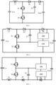
- this embodiment provides a boost circuit structure, including:
- the first controllable switch T1 and the second controllable switch T2 may be power switching transistors.
- the first controllable switch T1 is a first MOS transistor
- the second controllable switch T2 is a second MOS transistor.
- a drain of the first MOS transistor is connected to one terminal of the inductor L1
- a source of the first MOS transistor is connected to a drain of the second MOS transistor
- a source of the second MOS transistor is connected to the second input terminal of the boost circuit and the second output terminal of the boost circuit
- the other terminal of the inductor L1 is connected to the first input terminal of the boost circuit.
- the first input terminal and the second input terminal of the boost circuit are two terminals on the input side Cin of the boost circuit.
- the input side Cin of the boost circuit includes a positive input and a negative input, where when the first input terminal is the positive input, the second input terminal is the negative input; and when the first input terminal is the negative input, the second input terminal is the positive terminal.
- the anode of the first diode D1 is connected to the drain of the first MOS transistor, the cathode of the first diode D1 is connected to the anode of the second diode D2, and the cathode of the second diode D2 is connected to the first output terminal of the boost circuit.
- the first output terminal and the second output terminal of the boost circuit are two terminals on the output side Cout of the boost circuit.
- the output side Cout of the boost circuit includes a positive output and a negative output, where when the first output terminal is the positive output, the second output terminal is the negative output; and when the first output terminal is the negative output, the second output terminal is the positive output.
- one terminal of the flying capacitor C1 is connected to the source of the first MOS transistor, that is, one terminal of the flying capacitor C1 is connected to a line between the first MOS transistor and the second MOS transistor.
- the other terminal of the flying capacitor C1 is connected to the cathode of the first diode D1, that is, the other terminal of the flying capacitor C1 is connected to a line between the first diode D1 and the second diode D2.
- the first functional circuit 100 is connected to one terminal of the flying capacitor C1 and the second input terminal.
- the first functional circuit 100 may be a passive device or an active device that is configured to charge the flying capacitor C1 in a process of powering on the input side Cin, to protect the second controllable switch T2 from an overvoltage.
- the second functional circuit 200 is connected to the second diode D2 in parallel.
- the second functional circuit 200 may be a passive device or an active device that is configured to charge the flying capacitor C1 in a process of powering on the output side Cout, to protect the second diode D2 from an overvoltage.
- the boost circuit structure provided in this application may alternatively be adaptively transformed based on an actual requirement and a use environment, for example, transformed to a circuit structure shown in FIG. 3 . This is not limited herein.
- a boost circuit structure frame is formed by the switch circuit, the main boost circuit, and the branch boost circuit, and then the first functional circuit 100 is connected to the flying capacitor C1 and the second input terminal, to charge the flying capacitor C1 in the process of powering on the input side of the boost circuit, thereby protecting the second controllable switch T2 from the overvoltage.
- the second functional circuit 200 is connected to the second diode D2 in parallel, to charge the flying capacitor C1 in the process of powering on the output side of the boost circuit, thereby protecting the second diode D2 from the overvoltage.
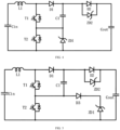
- the first functional circuit 100 includes a first Zener diode ZD1.
- a cathode of the first Zener diode ZD1 is connected to one terminal of the flying capacitor C1, and an anode of the first Zener diode ZD1 is connected to the second input terminal.
- the second functional circuit 200 includes a second Zener diode ZD2.
- An anode of the second Zener diode ZD2 is connected to the anode of the second diode D2, and a cathode of the second Zener diode ZD2 is connected to the cathode of the second diode D2.
- a voltage of the flying capacitor C1 is 0.
- the input side Cin forms a loop by using the inductor L1, the first diode D1, the flying capacitor C1, and the first Zener diode ZD 1, to charge the flying capacitor C1.
- a voltage of the second controllable switch T2 may be clamped to a preset voltage, to prevent the second controllable switch T2 from being damaged due to the overvoltage.
- a power of the first Zener diode ZD1 is associated with a capacitance of the flying capacitor C1.
- the voltage of the flying capacitor C1 when the output side Cout is powered on, the voltage of the flying capacitor C1 is 0.
- the output side Cout forms a loop by using the second Zener diode ZD2, the flying capacitor C1, an antiparallel diode of the first controllable switch T1, and the inductor L1, to charge the flying capacitor C1.
- a voltage of the second diode D2 may be clamped to a preset voltage, to prevent the second diode D2 from being damaged due to the overvoltage.
- a power of the second Zener diode ZD2 is associated with the capacitance of the flying capacitor C1.
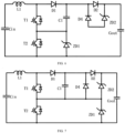
- the first functional circuit 100 further includes a third diode D3.
- the cathode of the first Zener diode ZD1 is connected to a cathode of the third diode D3, and is connected to one terminal of the flying capacitor C1 by using the third diode D3.
- the second functional circuit 200 further includes a fourth diode D4.
- the anode of the second Zener diode ZD2 is connected to an anode of the fourth diode D4, and is connected to the anode of the second diode D2 by using the fourth diode D4.
- the third diode D3 and the fourth diode D4 may be clamping diodes, and the first Zener diode ZD1 and the second Zener diode ZD2 are transient voltage suppression TVS diodes, voltage regulator diodes, or other similar discharge devices. This is not limited herein.
- the input side Cin when the input side Cin is powered on, the voltage of the flying capacitor C1 is 0. As shown in FIG. 10 , the input side Cin forms a loop by using the inductor L1, the first diode D1, the flying capacitor C1, the third diode D3, and the first Zener diode ZD1, to charge the flying capacitor C1. In the breakdown discharge process of the first Zener diode ZD1, the voltage of the second controllable switch T2 may be clamped to the preset voltage, to prevent the second controllable switch T2 from being damaged due to the overvoltage. The power of the first Zener diode ZD1 is associated with the capacitance of the flying capacitor C1.
- the voltage of the flying capacitor C1 is 0.
- the output side Cout forms a loop by using the second Zener diode ZD2, the fourth diode D4, the flying capacitor C1, the antiparallel diode of the first controllable switch T1, and the inductor L1, to charge the flying capacitor C1.
- the voltage of the second diode D2 may be clamped to the preset voltage, to prevent the second diode D2 from being damaged due to the overvoltage.
- the power of the second Zener diode ZD2 is associated with the capacitance of the flying capacitor C1.
- Use of passive devices such as a discharge clamp may reduce use of a capacitor, simplifies an operation state of a topology, and reduce system costs.
- the branch boost circuit further includes a first resistor R1
- the first functional circuit 100 further includes a second resistor R2.
- the first resistor R1 is connected to the flying capacitor C1 in parallel.
- the second resistor R2 is connected to the first Zener diode ZD1 in parallel.
- the second functional circuit 200 further includes a third resistor R3, and the third resistor R3 is connected to the second diode ZD2 in parallel.
- secondary precharging may be completed through impedance voltage division in a secondary precharging process of the flying capacitor C1.
- impedance voltage division-based secondary precharging process system complexity can be reduced.
- FIG. 12 in the process of powering on the input side Cin, voltage division is performed on the first resistor R1 and the second resistor R2, a loop is formed by the inductor L1, the first diode D1, the first resistor R1, the third diode D3, and the second resistor R2, to charge the voltage of the flying capacitor C1 to a preset voltage.
- one loop is formed by the third resistor R3, the first resistor R1, the antiparallel diode of the first controllable switch T1, the inductor L1, and the input side Cin and one loop is formed by the third resistor R3, the first resistor R1, the third diode D3, and the second resistor R2, to charge the voltage of the flying capacitor C1 to the preset voltage.
- the branch boost circuit further includes a fourth resistor R4 and a switch K1.
- One terminal of the switch K1 is connected to one terminal of the flying capacitor C1 by using the fourth resistor R4, and the other terminal of the switch K1 is connected to the second input terminal.
- secondary precharging may be completed by using an active device, namely, the switch K1.
- the switch K1 As shown in FIG. 14 , in the process of powering on the input side Cin, the voltage of the flying capacitor C1 is charged to the preset voltage by using a loop formed by the inductor L1, the first diode D1, the flying capacitor C1, the fourth resistor R4, and the switch K1.
- the voltage on the output side Cout is high, as shown in FIG.
- the voltage of the flying capacitor C1 may be charged to the preset voltage by using a loop formed by the second Zener diode ZD2, the fourth diode D4, the flying capacitor C1, the fourth resistor R4, and the switch K1. After the voltage of the flying capacitor C1 reaches the preset voltage, the switch K1 is disconnected from the main circuit.
- the functional unit devices in the foregoing circuit do not participate in operation in a normal operation process of the topology, and perform an action only in a power-on process or in an abnormal operation process of the circuit. Therefore, an operation status of the circuit and system heat are not affected.
- this application further provides an inverter apparatus, including the foregoing boost circuit structure.
- the inverter apparatus is an apparatus for converting a direct current into an alternating current, and may be used for various alternating current power supplies.
- the inverter apparatus includes a switch circuit, a main boost circuit, a branch boost circuit, a first functional circuit 100, and a second functional circuit 200, where the switch circuit includes a first controllable switch T1 and a second controllable switch T2 that are connected in series, one terminal of the first controllable switch T1 is connected to a first input terminal of a boost circuit by using an inductor L1, the other terminal of the first controllable switch T1 is connected to one terminal of the second controllable switch T2, and the other terminal of the second controllable switch T2 is connected to a second input terminal of the boost circuit and a second output terminal of the boost circuit.
- the main boost circuit includes a first diode D1 and a second diode D2.
- An anode of the first diode D1 is connected to one terminal of the first controllable switch T1, a cathode of the first diode D1 is connected to an anode of the second diode D2, and a cathode of the second diode D2 is connected to a first output terminal of the boost circuit.
- the branch boost circuit includes a flying capacitor C1, one terminal of the flying capacitor C1 is connected to the other terminal of the first controllable switch T1, and the other terminal of the flying capacitor C1 is connected to the cathode of the first diode D1.
- the first functional circuit 100 is connected to the flying capacitor C1 and the second input terminal, and is configured to charge the flying capacitor C1 when an input side of the boost circuit is powered on.
- the second functional circuit 200 is connected to the second diode D2 in parallel, and is configured to charge the flying capacitor C1 when an output side of the boost circuit is powered on.
- the first controllable switch and the second controllable switch may be power switching transistors.
- the first controllable switch T1 is a first MOS transistor
- the second controllable switch T2 is a second MOS transistor.
- a drain of the first MOS transistor is connected to one terminal of the inductor L1
- a source of the first MOS transistor is connected to a drain of the second MOS transistor
- a source of the second MOS transistor is connected to the second input terminal of the boost circuit and the second output terminal of the boost circuit
- the other terminal of the inductor L1 is connected to the first input terminal of the boost circuit.
- the first input terminal and the second input terminal of the boost circuit are two terminals on the input side Cin of the boost circuit.
- the input side Cin of the boost circuit includes a positive input and a negative input, where when the first input terminal is the positive input, the second input terminal is the negative input; and when the first input terminal is the negative input, the second input terminal is the positive terminal.
- the anode of the first diode D1 is connected to the drain of the first MOS transistor, the cathode of the first diode D1 is connected to the anode of the second diode D2, and the cathode of the second diode D2 is connected to the first output terminal of the boost circuit.
- the first output terminal and the second output terminal of the boost circuit are two terminals on the output side Cout of the boost circuit.
- the output side Cout of the boost circuit includes a positive output and a negative output, where when the first output terminal is the positive output, the second output terminal is the negative output; and when the first output terminal is the negative output, the second output terminal is the positive output.
- one terminal of the flying capacitor C1 is connected to the source of the first MOS transistor, that is, one terminal of the flying capacitor C1 is connected to a line between the first MOS transistor and the second MOS transistor.
- the other terminal of the flying capacitor C1 is connected to the cathode of the first diode D1, that is, the other terminal of the flying capacitor C1 is connected to a line between the first diode D1 and the second diode D2.
- the first functional circuit 100 is connected to one terminal of the flying capacitor C1 and the second input terminal.
- the first functional circuit 100 may be a passive device or an active device that is configured to charge the flying capacitor C1 in a process of powering on the input side Cin, to protect the second controllable switch T2 from an overvoltage.
- the second functional circuit 200 is connected to the second diode D2 in parallel.
- the second functional circuit 200 may be a passive device or an active device that is configured to charge the flying capacitor C1 in a process of powering on the output side Cout, to protect the second diode D2 from an overvoltage.
- a boost circuit structure frame is formed by the switch circuit, the main boost circuit, and the branch boost circuit, and then the first functional circuit 100 is connected to the flying capacitor C1 and the second input terminal, to charge the flying capacitor C1 in the process of powering on the input side of the boost circuit, thereby protecting the second controllable switch T2 from the overvoltage.
- the second functional circuit 200 is connected to the second diode D2 in parallel, to charge the flying capacitor C1 in the process of powering on the output side of the boost circuit, thereby protecting the second diode D2 from the overvoltage.
- this application further provides a photovoltaic power generation system, including the foregoing inverter apparatus.
Landscapes
- Engineering & Computer Science (AREA)
- Power Engineering (AREA)
- Dc-Dc Converters (AREA)
Applications Claiming Priority (2)
| Application Number | Priority Date | Filing Date | Title |
|---|---|---|---|
| CN202310157229.5A CN116155099A (zh) | 2023-02-23 | 2023-02-23 | 升压电路结构、逆变装置及光伏发电系统 |
| PCT/CN2023/089473 WO2024174369A1 (zh) | 2023-02-23 | 2023-04-20 | 升压电路结构、逆变装置及光伏发电系统 |
Publications (4)
| Publication Number | Publication Date |
|---|---|
| EP4459856A1 true EP4459856A1 (de) | 2024-11-06 |
| EP4459856A4 EP4459856A4 (de) | 2025-03-05 |
| EP4459856C0 EP4459856C0 (de) | 2025-12-24 |
| EP4459856B1 EP4459856B1 (de) | 2025-12-24 |
Family
ID=86354107
Family Applications (1)
| Application Number | Title | Priority Date | Filing Date |
|---|---|---|---|
| EP23772741.7A Active EP4459856B1 (de) | 2023-02-23 | 2023-04-20 | Verstärkerschaltungsstruktur, wechselrichtergerät und fotovoltaisches stromerzeugungssystem |
Country Status (4)
| Country | Link |
|---|---|
| US (1) | US20260018998A1 (de) |
| EP (1) | EP4459856B1 (de) |
| CN (1) | CN116155099A (de) |
| WO (1) | WO2024174369A1 (de) |
Families Citing this family (1)
| Publication number | Priority date | Publication date | Assignee | Title |
|---|---|---|---|---|
| DE102024204156A1 (de) * | 2024-05-03 | 2025-11-06 | Siemens Aktiengesellschaft | Aufwärtswandlerschaltanordnung |
Family Cites Families (19)
| Publication number | Priority date | Publication date | Assignee | Title |
|---|---|---|---|---|
| US8604757B2 (en) * | 2010-02-01 | 2013-12-10 | Mitsubishi Electric Corporation | DC/DC power conversion apparatus |
| US10581312B2 (en) * | 2017-12-29 | 2020-03-03 | Texas Instruments Incorporated | Multilevel converter using node voltage track and control |
| CN108258899B (zh) * | 2017-12-29 | 2021-06-15 | 华为技术有限公司 | 一种升压功率变换电路 |
| CN108847769B (zh) * | 2018-06-22 | 2020-03-24 | 阳光电源股份有限公司 | 一种三电平boost装置及其控制方法 |
| CN109756115B (zh) * | 2018-12-21 | 2021-12-03 | 华为数字技术(苏州)有限公司 | 一种升压功率变换电路、方法、逆变器、装置及系统 |
| CN112491270B (zh) * | 2019-09-12 | 2023-04-11 | 厦门科华数能科技有限公司 | 一种升压电路及其装置和系统 |
| CN110677027B (zh) * | 2019-09-26 | 2025-02-21 | 特变电工新疆新能源股份有限公司 | 一种嵌位型升压功率变换电路 |
| CN112701913A (zh) * | 2019-10-22 | 2021-04-23 | 阳光电源股份有限公司 | 升压功率变换电路及其控制方法与应用装置 |
| CN110943618A (zh) * | 2019-12-13 | 2020-03-31 | 科华恒盛股份有限公司 | 一种多电平升压电路及其装置和系统 |
| CN111245220B (zh) * | 2020-02-24 | 2025-01-24 | 上海正泰电源系统有限公司 | 三电平功率变换电路及电压钳位方法 |
| CN111245234B (zh) * | 2020-03-04 | 2025-07-04 | 厦门科华数能科技有限公司 | 一种升压电路及其装置和系统 |
| CN212381111U (zh) * | 2020-03-25 | 2021-01-19 | 上海正泰电源系统有限公司 | 一种可供飞跨电容预充电的三电平功率变换电路 |
| CN113765380B (zh) * | 2020-06-05 | 2024-08-20 | 台达电子工业股份有限公司 | 升压电路 |
| CN212909346U (zh) * | 2020-06-13 | 2021-04-06 | 深圳市禾望科技有限公司 | 升压功率变换电路 |
| CN112821761A (zh) * | 2021-02-03 | 2021-05-18 | 浙江日风电气股份有限公司 | 一种飞跨电容三电平boost电路 |
| CN112564483A (zh) * | 2021-02-23 | 2021-03-26 | 浙江日风电气股份有限公司 | 一种飞跨电容三电平Boost电路及其控制方法 |
| CN113098253B (zh) * | 2021-04-28 | 2022-10-18 | 厦门科华数能科技有限公司 | 一种功率变换电路 |
| US11689094B2 (en) * | 2021-05-19 | 2023-06-27 | Apple Inc. | Inductive flying capacitor converters and control techniques therefor |
| CN114552985A (zh) * | 2022-01-25 | 2022-05-27 | 厦门科华数能科技有限公司 | 一种升压电路、逆变装置及光伏发电装置 |
-
2023
- 2023-02-23 CN CN202310157229.5A patent/CN116155099A/zh active Pending
- 2023-04-20 WO PCT/CN2023/089473 patent/WO2024174369A1/zh not_active Ceased
- 2023-04-20 US US18/995,176 patent/US20260018998A1/en active Pending
- 2023-04-20 EP EP23772741.7A patent/EP4459856B1/de active Active
Also Published As
| Publication number | Publication date |
|---|---|
| WO2024174369A1 (zh) | 2024-08-29 |
| EP4459856C0 (de) | 2025-12-24 |
| US20260018998A1 (en) | 2026-01-15 |
| EP4459856B1 (de) | 2025-12-24 |
| EP4459856A4 (de) | 2025-03-05 |
| CN116155099A (zh) | 2023-05-23 |
Similar Documents
| Publication | Publication Date | Title |
|---|---|---|
| CA3050229C (en) | Shutdown apparatus for photovoltaic module | |
| KR101489563B1 (ko) | 역접속 보호 장치 및 이를 포함하는 예비 전원 공급장치 | |
| US12444950B2 (en) | Control method and apparatus for shut-off device and shut-off device | |
| EP3920359B1 (de) | Invertervorrichtung und energieversorgungssystem | |
| CN110943618A (zh) | 一种多电平升压电路及其装置和系统 | |
| CN107834826A (zh) | 电源控制模块 | |
| US12500424B2 (en) | Power supply system and solar photovoltaic inverter | |
| CN110912386A (zh) | 主动放电电路 | |
| EP4459856A1 (de) | Verstärkerschaltungsstruktur, wechselrichtervorrichtung und fotovoltaisches stromerzeugungssystem | |
| CN118213943B (zh) | 一种适用于串联SiC MOSFET的短路保护电路 | |
| CN115241959A (zh) | 可自动充电激活锂电池包的免维护储能电源及其控制方法 | |
| US20230387807A1 (en) | Charging circuit and charging apparatus | |
| CN111884255A (zh) | 一种光伏逆变器及光伏系统 | |
| US20140001862A1 (en) | Uninterruptible power supply | |
| CN212909346U (zh) | 升压功率变换电路 | |
| CN112491270B (zh) | 一种升压电路及其装置和系统 | |
| CN218335753U (zh) | 一种用于机通设备的acu电源板 | |
| CN118920687A (zh) | 一种ups电源安全检测控制装置 | |
| WO2022183446A1 (zh) | 一种检测电路, 防反灌系统及充电桩 | |
| CN110061692B (zh) | 针对串联式光伏组件的关断系统及其重新启动的方法 | |
| US11784494B2 (en) | Direct current power supply system, photovoltaic system, energy storage system, and optical storage system | |
| WO2022233147A1 (zh) | 充电保护电路模块及相关产品 | |
| CN212435364U (zh) | 一种光伏逆变器的系统电源供电装置及光伏逆变器 | |
| WO2022257215A1 (zh) | 一种关断器的控制方法、装置及关断器 | |
| CN219145107U (zh) | 一种基于直流母线的无线供电电路 |
Legal Events
| Date | Code | Title | Description |
|---|---|---|---|
| STAA | Information on the status of an ep patent application or granted ep patent |
Free format text: STATUS: UNKNOWN |
|
| STAA | Information on the status of an ep patent application or granted ep patent |
Free format text: STATUS: THE INTERNATIONAL PUBLICATION HAS BEEN MADE |
|
| PUAI | Public reference made under article 153(3) epc to a published international application that has entered the european phase |
Free format text: ORIGINAL CODE: 0009012 |
|
| STAA | Information on the status of an ep patent application or granted ep patent |
Free format text: STATUS: REQUEST FOR EXAMINATION WAS MADE |
|
| 17P | Request for examination filed |
Effective date: 20230928 |
|
| AK | Designated contracting states |
Kind code of ref document: A1 Designated state(s): AL AT BE BG CH CY CZ DE DK EE ES FI FR GB GR HR HU IE IS IT LI LT LU LV MC ME MK MT NL NO PL PT RO RS SE SI SK SM TR |
|
| A4 | Supplementary search report drawn up and despatched |
Effective date: 20250205 |
|
| RIC1 | Information provided on ipc code assigned before grant |
Ipc: H02M 1/36 20070101ALI20250130BHEP Ipc: H02M 1/32 20070101ALI20250130BHEP Ipc: H02M 1/00 20060101ALI20250130BHEP Ipc: H02M 3/158 20060101AFI20250130BHEP |
|
| GRAP | Despatch of communication of intention to grant a patent |
Free format text: ORIGINAL CODE: EPIDOSNIGR1 |
|
| STAA | Information on the status of an ep patent application or granted ep patent |
Free format text: STATUS: GRANT OF PATENT IS INTENDED |
|
| DAV | Request for validation of the european patent (deleted) | ||
| DAX | Request for extension of the european patent (deleted) | ||
| INTG | Intention to grant announced |
Effective date: 20250630 |
|
| GRAS | Grant fee paid |
Free format text: ORIGINAL CODE: EPIDOSNIGR3 |
|
| GRAA | (expected) grant |
Free format text: ORIGINAL CODE: 0009210 |
|
| STAA | Information on the status of an ep patent application or granted ep patent |
Free format text: STATUS: THE PATENT HAS BEEN GRANTED |
|
| AK | Designated contracting states |
Kind code of ref document: B1 Designated state(s): AL AT BE BG CH CY CZ DE DK EE ES FI FR GB GR HR HU IE IS IT LI LT LU LV MC ME MK MT NL NO PL PT RO RS SE SI SK SM TR |
|
| REG | Reference to a national code |
Ref country code: CH Ref legal event code: F10 Free format text: ST27 STATUS EVENT CODE: U-0-0-F10-F00 (AS PROVIDED BY THE NATIONAL OFFICE) Effective date: 20251224 Ref country code: GB Ref legal event code: FG4D |
|
| REG | Reference to a national code |
Ref country code: DE Ref legal event code: R096 Ref document number: 602023010182 Country of ref document: DE |
|
| U01 | Request for unitary effect filed |
Effective date: 20251224 |
|
| U07 | Unitary effect registered |
Designated state(s): AT BE BG DE DK EE FI FR IT LT LU LV MT NL PT RO SE SI Effective date: 20260107 |
|
| PG25 | Lapsed in a contracting state [announced via postgrant information from national office to epo] |
Ref country code: NO Free format text: LAPSE BECAUSE OF FAILURE TO SUBMIT A TRANSLATION OF THE DESCRIPTION OR TO PAY THE FEE WITHIN THE PRESCRIBED TIME-LIMIT Effective date: 20260324 |
|
| PG25 | Lapsed in a contracting state [announced via postgrant information from national office to epo] |
Ref country code: HR Free format text: LAPSE BECAUSE OF FAILURE TO SUBMIT A TRANSLATION OF THE DESCRIPTION OR TO PAY THE FEE WITHIN THE PRESCRIBED TIME-LIMIT Effective date: 20251224 |
|
| PG25 | Lapsed in a contracting state [announced via postgrant information from national office to epo] |
Ref country code: RS Free format text: LAPSE BECAUSE OF FAILURE TO SUBMIT A TRANSLATION OF THE DESCRIPTION OR TO PAY THE FEE WITHIN THE PRESCRIBED TIME-LIMIT Effective date: 20260324 |