EP4456525A1 - Image capture device - Google Patents
Image capture device Download PDFInfo
- Publication number
- EP4456525A1 EP4456525A1 EP23170457.8A EP23170457A EP4456525A1 EP 4456525 A1 EP4456525 A1 EP 4456525A1 EP 23170457 A EP23170457 A EP 23170457A EP 4456525 A1 EP4456525 A1 EP 4456525A1
- Authority
- EP
- European Patent Office
- Prior art keywords
- image capture
- capture device
- electromagnetic shield
- face
- circuit board
- Prior art date
- Legal status (The legal status is an assumption and is not a legal conclusion. Google has not performed a legal analysis and makes no representation as to the accuracy of the status listed.)
- Pending
Links
Images

Classifications
-
- H—ELECTRICITY
- H04—ELECTRIC COMMUNICATION TECHNIQUE
- H04N—PICTORIAL COMMUNICATION, e.g. TELEVISION
- H04N23/00—Cameras or camera modules comprising electronic image sensors; Control thereof
- H04N23/50—Constructional details
- H04N23/52—Elements optimising image sensor operation, e.g. for electromagnetic interference [EMI] protection or temperature control by heat transfer or cooling elements
-
- H—ELECTRICITY
- H04—ELECTRIC COMMUNICATION TECHNIQUE
- H04N—PICTORIAL COMMUNICATION, e.g. TELEVISION
- H04N23/00—Cameras or camera modules comprising electronic image sensors; Control thereof
- H04N23/50—Constructional details
- H04N23/51—Housings
-
- H—ELECTRICITY
- H04—ELECTRIC COMMUNICATION TECHNIQUE
- H04N—PICTORIAL COMMUNICATION, e.g. TELEVISION
- H04N23/00—Cameras or camera modules comprising electronic image sensors; Control thereof
- H04N23/50—Constructional details
- H04N23/54—Mounting of pick-up tubes, electronic image sensors, deviation or focusing coils
-
- H—ELECTRICITY
- H04—ELECTRIC COMMUNICATION TECHNIQUE
- H04N—PICTORIAL COMMUNICATION, e.g. TELEVISION
- H04N23/00—Cameras or camera modules comprising electronic image sensors; Control thereof
- H04N23/50—Constructional details
- H04N23/55—Optical parts specially adapted for electronic image sensors; Mounting thereof
-
- H—ELECTRICITY
- H04—ELECTRIC COMMUNICATION TECHNIQUE
- H04N—PICTORIAL COMMUNICATION, e.g. TELEVISION
- H04N23/00—Cameras or camera modules comprising electronic image sensors; Control thereof
- H04N23/56—Cameras or camera modules comprising electronic image sensors; Control thereof provided with illuminating means
Definitions
- the invention relates to the field of electronic devices, and in particular to the field of housing for electronic device.
- the invention relates to an image capture device.
- one object of the invention is to provide a image capture apparatus with a reduced production cost and a simpler assembling.
- the infrared transparent material being overmoulded on the front electromagnetic shield, the number of pieces of the front portion is reduced by one, which simplify the assembling and enable a reduction of the cost of the device.
- the image capture device comprises an optical lens configured to focus light rays directed through the aperture towards the image sensor, the optical lens being attached to the electronic circuit board.
- the optical lens is fixed to a frame which is glued to the electronic circuit board.
- the first face comprises at least an infrared light source facing a second aperture in the front electromagnetic shield
- the front electromagnetic shield comprises an opaque portion extending between the infrared light source and the lens and configured to prevent light emitted by the infrared light source to go directly into the lens
- the rear portion comprises a rear electromagnetic shield and a polymer material overmoulded over the rear electromagnetic shield.
- the polymer material comprises polybutylene terephthalate.
- the front electromagnetic shield is thermally coupled with the electronic circuit board and comprises metal, for instance aluminum, copper or stainless steel.
- the rear electromagnetic shield is thermally coupled with the electronic circuit board and comprises metal, for instance aluminum, copper or stainless steel.
- the housing has a protection index of at least IPX1 with respect to the IEC 60529 standard, and preferably at least IP52.
- the infrared transparent material comprises polycarbonate.
- An image capture device as depicted in figures 1 to 3 and designated as a whole by the reference 1, comprises a two-portion housing 2, 3 enclosing an electronic circuit board 4.
- the electronic circuit board 4 comprises a first face 5 and a second face 6 opposite to the first face 5.
- the two-portion housing comprise a front portion 2 configured to face the first face 5 of the electronic circuit board 4 and a rear portion 3 configured to face the second face 6 of the electronic circuit board 4.
- the first portion 2 and the second portion 3 are configured to be assembled in order to form the housing enclosing the electronic circuit board 4, as apparent on figure 2 .
- the rear portion 3 comprises a rear electromagnetic shield 9 overmoulded with a polymer material, here polybutylene terephthalate.
- the rear electromagnetic shield 9 comprises several protrusions 11 extending from the periphery of the electromagnetic shield (here four protrusions, only one of which having a numeral referenced in the figures for clarity purpose), orthogonally to the first face 5 and second face 6 and configured to be directed toward the front portion 2.
- the protrusion 11 are rectilinear strip and the dimensions of the rear portion 2 are such that, when the second face 6 is placed against the rear portion 2, the protrusions 11 prevent the movements of the electronic circuit board 4 in any direction parallel to the first faces 5 or to the second face 6.
- the front portion 3 comprises a front electromagnetic shield 12 overmoulded with an infrared transparent material 13, for instance here a material that is transparent for infrared light and opaque for visible light.
- the front electromagnetic shield 12 is made in an opaque material and comprises a main aperture 14 configured to let light through to the image sensor 7.
- Two secondary apertures 15 are configured to let the light emitted by the light sources exit the housing.
- the infrared transparent material 13 encloses the electromagnetic shield so it covers the front electromagnetic shield surface (except for some bare areas described hereafter) and so it mechanically obstructs the apertures 14 and 15. Thus, the components of the electronic circuit board are protected and the light is not obstructed.
- fixation means here two screws 17 configured each to be inserted in a plurality of coaxial holes made in the front portion 2, in the rear portion 3 and in the electronic circuit board 4.
- the front electromagnetic shield 12 and the rear electromagnetic shield 9 are at least electrically coupled (with or without direct contact), and preferably directly connected (with a direct contact).
- the inner wall of the front portion 2 comprises several bare areas 18 where the front electromagnetic field 12 is devoid of infrared transparent material. These bare areas 18 are located such that, when the front portion 2 and the rear portion 3 are assembled, the protrusions 11 are in direct contact with the bare areas 18.
- the screws are conductive and in contact with the front electromagnetic shield 12, the rear electromagnetic shield 9, and the electronic circuit board 4, thus they ensure an electrical coupling between the front electromagnetic shield 12 and the rear electromagnetic shield 9.
- the front electromagnetic shield 12 comprises opaque portion 20 extending between the lens 19 and the light sources 8 and configured to prevent light emitted by the light sources 8 to go directly into the lens 19.
- the opaque portion 20 form a tunnel extending toward the first face, around the lens 19 and the frame 16, an extremity of which defining the outlines of the main aperture 14.
- the electromagnetic shields 9 and/or 12 may comprise any electrically conductive material.
- they comprise a material that gives it a rigidity sufficient to absorbs moderate shocks.
- the electromagnetic shields 9 and/or 12 comprise a material having a thermal conductivity sufficient to act as a heat sink.
- the electromagnetic shield 9, 12 comprise a metal, for instance aluminum, copper, or stainless steel.
- the infrared transparent material 13 is preferably a plastic material and preferably polycarbonate.
- the polymer material 10 is preferably polybutylene terephthalate.
- the image capture device is an infrared image capture device. Therefore, the image sensor 7 is sensitive to infrared light and the light sources 8 are configured to emit infrared light. In application other than driver monitoring, the image capture device may be configured to capture light having other wavelengths, for instance wavelengths in the visible spectrum.
- the housing 2,3 described above is configured to protect the electronic circuit board 4 against water. It has a protection index of at least IP52 with respect to the IEC 60529 standard or, in other words, it provides an effective protection against dripping water. In order to comply with higher protection indexes, seals may be added between the two electromagnetic shields 9, 12 and/or between the electromagnetic shields and the electronic circuit board 4.
- the image capture device is not limited by the presence of light sources, nor it is by the number of the light sources.
- Other embodiments of the invention comprise no light source or only one light source.
- fixation means being screws
- fixation means for instance a clipping system, glue, rivets, etc.
- an opaque portion 20 extending around the lens in order to prevent light emitted by the light sources to reach directly the lens.
- the shape and location of this opaque portion is not limitative.
- the invention is compatible with opaque portions placed around the light sources, or around both the light sources and the lens. In such cases, the opaque portions placed around the light source act as reflectors.
Landscapes
- Engineering & Computer Science (AREA)
- Multimedia (AREA)
- Signal Processing (AREA)
- Physics & Mathematics (AREA)
- Electromagnetism (AREA)
- Studio Devices (AREA)
- Photometry And Measurement Of Optical Pulse Characteristics (AREA)
Abstract
Description
- The invention relates to the field of electronic devices, and in particular to the field of housing for electronic device.
- More precisely the invention relates to an image capture device.
- In order to integrate electronic devices in larger systems, it is known to protect or hide them with a housing. For instance, some automotive vehicles are equipped with one or several image capture apparatuses configured to perform driver monitoring. Such devices typically comprise an integrated circuit board protected by an electromagnetic shield and by a polymeric transparent casing. The electromagnetic shield ensures the electromagnetic compatibility of the device a gives it a certain rigidity. The polymeric transparent casing protects the parts of the device that are not covered by the electromagnetic shield, for instance a lens or a light source. Those two parts are assembled in order to form the housing of the device. A need exists for reducing the production cost of such device and to simplify their assembling.
- Therefore one object of the invention is to provide a image capture apparatus with a reduced production cost and a simpler assembling.
- According to an aspect of the invention, it is provided an image capture device comprising a housing enclosing an electronic circuit board having an image sensor attached to a first face thereof, the housing comprising a front portion facing the first face and a rear portion facing a second face opposite the first face, the front portion comprising a front electromagnetic shield having an aperture facing the image sensor and an infra-red transparent material overmoulded onto the electromagnetic shield and mechanically obstructing the aperture.
- Thanks to the infrared transparent material being overmoulded on the front electromagnetic shield, the number of pieces of the front portion is reduced by one, which simplify the assembling and enable a reduction of the cost of the device.
- According to an embodiment, the image capture device comprises an optical lens configured to focus light rays directed through the aperture towards the image sensor, the optical lens being attached to the electronic circuit board.
- According to an embodiment, the optical lens is fixed to a frame which is glued to the electronic circuit board.
- According to an embodiment, the first face comprises at least an infrared light source facing a second aperture in the front electromagnetic shield, and/or the front electromagnetic shield comprises an opaque portion extending between the infrared light source and the lens and configured to prevent light emitted by the infrared light source to go directly into the lens.
- According to an embodiment, the rear portion comprises a rear electromagnetic shield and a polymer material overmoulded over the rear electromagnetic shield.
- According to an embodiment, the polymer material comprises polybutylene terephthalate.
- According to an embodiment, the front electromagnetic shield is thermally coupled with the electronic circuit board and comprises metal, for instance aluminum, copper or stainless steel.
- According to an embodiment, the rear electromagnetic shield is thermally coupled with the electronic circuit board and comprises metal, for instance aluminum, copper or stainless steel.
- According to an embodiment, the housing has a protection index of at least IPX1 with respect to the IEC 60529 standard, and preferably at least IP52.
- According to an embodiment, the infrared transparent material comprises polycarbonate.
- The following description with reference to the accompanying drawings will make it clear what the invention consists of and how it can be achieved. The invention is not limited to the embodiments illustrated in the drawings. Accordingly, it should be understood that where features mentioned in the claims are followed by reference signs, such signs are included solely for the purpose of enhancing the intelligibility of the claims and are in no way limiting on the scope of the claims.
- In the accompanying drawings:
-
Figure 1 is an exploded view of an image apparatus device according to the invention, -
Figure 2 is a cross sectional view of the device offigure 1 , -
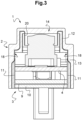
Figure 3 is a cross sectional view of the device offigure 1 , along the section line III-III offigure 2 . - An image capture device according to an embodiment of the invention, as depicted in
figures 1 to 3 and designated as a whole by thereference 1, comprises a two-portion housing electronic circuit board 4. - Here, the
electronic circuit board 4 comprises afirst face 5 and asecond face 6 opposite to thefirst face 5. An image sensor 7, for instance a matrix of pixels, and at least a light source, here twolight sources 8, are fixed on thefirst face 5. Alens 19 mounted on a frame fixed to thefirst face 5, for instance glued to the first face 5 - is located in front of the image sensor. - The two-portion housing comprise a
front portion 2 configured to face thefirst face 5 of theelectronic circuit board 4 and arear portion 3 configured to face thesecond face 6 of theelectronic circuit board 4. Thefirst portion 2 and thesecond portion 3 are configured to be assembled in order to form the housing enclosing theelectronic circuit board 4, as apparent onfigure 2 . - The
rear portion 3 comprises a rearelectromagnetic shield 9 overmoulded with a polymer material, here polybutylene terephthalate. The rearelectromagnetic shield 9 comprisesseveral protrusions 11 extending from the periphery of the electromagnetic shield (here four protrusions, only one of which having a numeral referenced in the figures for clarity purpose), orthogonally to thefirst face 5 andsecond face 6 and configured to be directed toward thefront portion 2. Here, theprotrusion 11 are rectilinear strip and the dimensions of therear portion 2 are such that, when thesecond face 6 is placed against therear portion 2, theprotrusions 11 prevent the movements of theelectronic circuit board 4 in any direction parallel to thefirst faces 5 or to thesecond face 6. - The
front portion 3 comprises a frontelectromagnetic shield 12 overmoulded with an infraredtransparent material 13, for instance here a material that is transparent for infrared light and opaque for visible light. The frontelectromagnetic shield 12 is made in an opaque material and comprises amain aperture 14 configured to let light through to the image sensor 7. Twosecondary apertures 15 are configured to let the light emitted by the light sources exit the housing. The infraredtransparent material 13 encloses the electromagnetic shield so it covers the front electromagnetic shield surface (except for some bare areas described hereafter) and so it mechanically obstructs theapertures - The assembly of the
front portion 2, therear portion 3 and theelectronic circuit board 4 is ensured by fixation means, here twoscrews 17 configured each to be inserted in a plurality of coaxial holes made in thefront portion 2, in therear portion 3 and in theelectronic circuit board 4. - In order to ensure a more reliable electromagnetic isolation, the front
electromagnetic shield 12 and the rearelectromagnetic shield 9 are at least electrically coupled (with or without direct contact), and preferably directly connected (with a direct contact). - As apparent on
figure 3 , the inner wall of thefront portion 2 comprises severalbare areas 18 where the frontelectromagnetic field 12 is devoid of infrared transparent material. Thesebare areas 18 are located such that, when thefront portion 2 and therear portion 3 are assembled, theprotrusions 11 are in direct contact with thebare areas 18. - Here, the screws are conductive and in contact with the front
electromagnetic shield 12, the rearelectromagnetic shield 9, and theelectronic circuit board 4, thus they ensure an electrical coupling between the frontelectromagnetic shield 12 and the rearelectromagnetic shield 9. - In this embodiment, the front
electromagnetic shield 12 comprisesopaque portion 20 extending between thelens 19 and thelight sources 8 and configured to prevent light emitted by thelight sources 8 to go directly into thelens 19. For instance, theopaque portion 20 form a tunnel extending toward the first face, around thelens 19 and theframe 16, an extremity of which defining the outlines of themain aperture 14. - The different elements of the above-described device are not limited by the material they are made of, as long as the material is suitable with their function. For instance, the
electromagnetic shields 9 and/or 12 may comprise any electrically conductive material. Preferably, they comprise a material that gives it a rigidity sufficient to absorbs moderate shocks. Preferably, theelectromagnetic shields 9 and/or 12 comprise a material having a thermal conductivity sufficient to act as a heat sink. For instance, theelectromagnetic shield - The infrared
transparent material 13 is preferably a plastic material and preferably polycarbonate. Thepolymer material 10 is preferably polybutylene terephthalate. - Here, the image capture device is an infrared image capture device. Therefore, the image sensor 7 is sensitive to infrared light and the
light sources 8 are configured to emit infrared light. In application other than driver monitoring, the image capture device may be configured to capture light having other wavelengths, for instance wavelengths in the visible spectrum. - The
housing electronic circuit board 4 against water. It has a protection index of at least IP52 with respect to the IEC 60529 standard or, in other words, it provides an effective protection against dripping water. In order to comply with higher protection indexes, seals may be added between the twoelectromagnetic shields electronic circuit board 4. - The invention is not limited to the embodiment described above in connection with
figures 1 to 3 . - For instance, the image capture device is not limited by the presence of light sources, nor it is by the number of the light sources. Other embodiments of the invention comprise no light source or only one light source.
- The invention is not limited to fixation means being screws, but is compatible with any fixation means, for instance a clipping system, glue, rivets, etc.
- It has been described an
opaque portion 20 extending around the lens in order to prevent light emitted by the light sources to reach directly the lens. The shape and location of this opaque portion is not limitative. For instance, the invention is compatible with opaque portions placed around the light sources, or around both the light sources and the lens. In such cases, the opaque portions placed around the light source act as reflectors.
Claims (10)
- An image capture device comprising a housing enclosing an electronic circuit board (4) having an image sensor (7) attached to a first face (5) thereof, the housing comprising a front portion (2) facing the first face (5) and a rear portion (3) facing a second face (6) opposite the first face (5), the front portion (2) comprising a front electromagnetic shield (12) having an aperture (14) facing the image sensor (7) and an infra-red transparent material (13) overmoulded onto the front electromagnetic shield (12) and mechanically obstructing the aperture (14).
- The image capture device according to claim 1, comprising an optical lens (19) configured to focus light rays directed through the aperture (14) towards the image sensor (7), the optical lens (19) being attached to the electronic circuit board (4).
- The image capture device according to claim 2, wherein the optical lens (19) is fixed to a frame (16) which is glued to the electronic circuit board (4).
- The image capture device according to claims 2 or 3, wherein the first face (5) comprises at least an infrared light source (8) facing a second aperture (15) in the front electromagnetic shield (12), the front electromagnetic shield (12) comprising an opaque portion (20) extending between the infrared light source (8) and the lens (19) and configured to prevent light emitted by the infrared light source (8) to go directly into the lens (19).
- The image capture device according to any one of claims 1 to 4, wherein the rear portion (3) comprises a rear electromagnetic shield (9) and a polymer material (10) overmoulded over the rear electromagnetic shield (9).
- The image capture device according to claim 5, wherein the polymer material (10) comprises polybutylene terephthalate.
- The image capture device according to any one of claims 5 or 6, wherein the front electromagnetic shield (12) is thermally coupled with the electronic circuit board (4) and comprises metal.
- The image capture device according to any one of claims 1 to 7, wherein the rear electromagnetic shield (9) is thermally coupled with the electronic circuit board (4) and comprises metal.
- The image capture device according to any one of claims 1 to 8, wherein the housing (2,3) has a protection index of at least IP52 with respect to the IEC 60529 standard.
- The image capture device according to any one of claims 1 to 8, wherein the infrared transparent material (13) comprises polycarbonate.
Priority Applications (3)
| Application Number | Priority Date | Filing Date | Title |
|---|---|---|---|
| EP23170457.8A EP4456525A1 (en) | 2023-04-27 | 2023-04-27 | Image capture device |
| US18/646,909 US12647662B2 (en) | 2023-04-27 | 2024-04-26 | Image capture device |
| CN202410522665.2A CN118870169A (en) | 2023-04-27 | 2024-04-28 | Image capture device |
Applications Claiming Priority (1)
| Application Number | Priority Date | Filing Date | Title |
|---|---|---|---|
| EP23170457.8A EP4456525A1 (en) | 2023-04-27 | 2023-04-27 | Image capture device |
Publications (1)
| Publication Number | Publication Date |
|---|---|
| EP4456525A1 true EP4456525A1 (en) | 2024-10-30 |
Family
ID=86272342
Family Applications (1)
| Application Number | Title | Priority Date | Filing Date |
|---|---|---|---|
| EP23170457.8A Pending EP4456525A1 (en) | 2023-04-27 | 2023-04-27 | Image capture device |
Country Status (3)
| Country | Link |
|---|---|
| US (1) | US12647662B2 (en) |
| EP (1) | EP4456525A1 (en) |
| CN (1) | CN118870169A (en) |
Families Citing this family (2)
| Publication number | Priority date | Publication date | Assignee | Title |
|---|---|---|---|---|
| CN119620513A (en) * | 2024-12-10 | 2025-03-14 | 维沃移动通信有限公司 | Camera modules and electronic equipment |
| JP7827125B1 (en) * | 2024-12-27 | 2026-03-10 | Toppanホールディングス株式会社 | Range imaging device |
Citations (5)
| Publication number | Priority date | Publication date | Assignee | Title |
|---|---|---|---|---|
| US20090195897A1 (en) * | 2008-02-03 | 2009-08-06 | Chia-Hsi Tsai | Lens module and method for making the same |
| US20180338021A1 (en) * | 2015-06-10 | 2018-11-22 | Fairphone B.V. | Electronic device |
| US20200195816A1 (en) * | 2018-12-12 | 2020-06-18 | Valeo North America, Inc. | Common cover lens for camera and illuminators |
| DE102020211194A1 (en) * | 2020-09-07 | 2022-03-10 | Robert Bosch Gesellschaft mit beschränkter Haftung | Housing arrangement and method for manufacturing a housing arrangement |
| WO2022180051A1 (en) * | 2021-02-23 | 2022-09-01 | Solvay Specialty Polymers Usa, Llc | Polyamide compositions with functionalized polyolefin and mobile electronic device components containing them |
Family Cites Families (12)
| Publication number | Priority date | Publication date | Assignee | Title |
|---|---|---|---|---|
| US6266197B1 (en) * | 1999-12-08 | 2001-07-24 | Amkor Technology, Inc. | Molded window array for image sensor packages |
| US6807731B2 (en) * | 2002-04-02 | 2004-10-26 | Delphi Technologies, Inc. | Method for forming an electronic assembly |
| WO2008133946A1 (en) * | 2007-04-24 | 2008-11-06 | Flextronics Ap Llc | Auto focus/ zoom modules using wafer level optics |
| US8906515B2 (en) * | 2009-06-02 | 2014-12-09 | Integran Technologies, Inc. | Metal-clad polymer article |
| KR20130030067A (en) * | 2011-09-16 | 2013-03-26 | 엘지이노텍 주식회사 | Camera module and portable terminal with the same |
| US9621773B2 (en) * | 2013-02-22 | 2017-04-11 | Heptagon Micro Optics Pte. Ltd. | Optical imaging apparatus, in particular for computational imaging, having further functionality |
| KR102213027B1 (en) * | 2016-03-16 | 2021-02-04 | 젠텍스 코포레이션 | Camera assembly with shielded imager circuit |
| US20180295262A1 (en) * | 2017-04-06 | 2018-10-11 | Ford Global Technologies, Llc | Conductive emi-shield housings for vehicle cameras |
| KR102488006B1 (en) * | 2018-03-20 | 2023-01-12 | 엘지이노텍 주식회사 | Camera module and optical instrument including the same |
| CN112888282B (en) * | 2019-11-29 | 2022-08-19 | 华为终端有限公司 | Shielding device and electronic equipment |
| EP4109173B1 (en) * | 2020-02-19 | 2025-10-01 | Sony Semiconductor Solutions Corporation | Camera module |
| US12055633B2 (en) * | 2020-08-25 | 2024-08-06 | Lumentum Operations Llc | Package for a time of flight device |
-
2023
- 2023-04-27 EP EP23170457.8A patent/EP4456525A1/en active Pending
-
2024
- 2024-04-26 US US18/646,909 patent/US12647662B2/en active Active
- 2024-04-28 CN CN202410522665.2A patent/CN118870169A/en active Pending
Patent Citations (5)
| Publication number | Priority date | Publication date | Assignee | Title |
|---|---|---|---|---|
| US20090195897A1 (en) * | 2008-02-03 | 2009-08-06 | Chia-Hsi Tsai | Lens module and method for making the same |
| US20180338021A1 (en) * | 2015-06-10 | 2018-11-22 | Fairphone B.V. | Electronic device |
| US20200195816A1 (en) * | 2018-12-12 | 2020-06-18 | Valeo North America, Inc. | Common cover lens for camera and illuminators |
| DE102020211194A1 (en) * | 2020-09-07 | 2022-03-10 | Robert Bosch Gesellschaft mit beschränkter Haftung | Housing arrangement and method for manufacturing a housing arrangement |
| WO2022180051A1 (en) * | 2021-02-23 | 2022-09-01 | Solvay Specialty Polymers Usa, Llc | Polyamide compositions with functionalized polyolefin and mobile electronic device components containing them |
Also Published As
| Publication number | Publication date |
|---|---|
| CN118870169A (en) | 2024-10-29 |
| US20240364986A1 (en) | 2024-10-31 |
| US12647662B2 (en) | 2026-06-02 |
Similar Documents
| Publication | Publication Date | Title |
|---|---|---|
| US20240364986A1 (en) | Image capture device | |
| KR102213027B1 (en) | Camera assembly with shielded imager circuit | |
| US9596397B2 (en) | Dual shot strobe lens and flex and stiffener features of a camera | |
| CN114624942B (en) | camera module | |
| EP3895413B1 (en) | Common cover lens for camera and illuminators | |
| EP3163864B1 (en) | Image-capturing device and vehicle | |
| US5233676A (en) | Optical module | |
| WO2019032225A1 (en) | Bracket assembly for a multi-component vision system in an electronic device | |
| JP7541844B2 (en) | Imaging device and vehicle | |
| JP2009288484A (en) | Light emitting display | |
| CN105318226A (en) | Lighting device | |
| JP7028589B2 (en) | Imaging device | |
| JP2013075608A (en) | Lighting fixture for vehicle | |
| TWM577525U (en) | Electronic device and camera module thereof | |
| EP3163158A1 (en) | Light emitting diode signal module | |
| US11312314B2 (en) | Vehicle camera | |
| KR20210154520A (en) | Camera modure | |
| EP1248129B1 (en) | Optical connector | |
| US20160234982A1 (en) | Housing and control unit having a housing | |
| CN101241658B (en) | Electronic apparatus with light emitting diode | |
| KR20200055548A (en) | Camera Module | |
| US10286836B2 (en) | Automotive lighting device with signaling function | |
| KR20220049199A (en) | Camera module | |
| JP7161472B2 (en) | Imaging device | |
| CN119563381A (en) | Lighting devices for motor vehicles |
Legal Events
| Date | Code | Title | Description |
|---|---|---|---|
| PUAI | Public reference made under article 153(3) epc to a published international application that has entered the european phase |
Free format text: ORIGINAL CODE: 0009012 |
|
| STAA | Information on the status of an ep patent application or granted ep patent |
Free format text: STATUS: THE APPLICATION HAS BEEN PUBLISHED |
|
| AK | Designated contracting states |
Kind code of ref document: A1 Designated state(s): AL AT BE BG CH CY CZ DE DK EE ES FI FR GB GR HR HU IE IS IT LI LT LU LV MC ME MK MT NL NO PL PT RO RS SE SI SK SM TR |
|
| STAA | Information on the status of an ep patent application or granted ep patent |
Free format text: STATUS: REQUEST FOR EXAMINATION WAS MADE |
|
| 17P | Request for examination filed |
Effective date: 20250423 |
|
| GRAP | Despatch of communication of intention to grant a patent |
Free format text: ORIGINAL CODE: EPIDOSNIGR1 |
|
| STAA | Information on the status of an ep patent application or granted ep patent |
Free format text: STATUS: GRANT OF PATENT IS INTENDED |
|
| INTG | Intention to grant announced |
Effective date: 20260709 |