EP4456423A1 - Frequency generator and frequency correction method for frequency generator - Google Patents
Frequency generator and frequency correction method for frequency generator Download PDFInfo
- Publication number
- EP4456423A1 EP4456423A1 EP22911773.4A EP22911773A EP4456423A1 EP 4456423 A1 EP4456423 A1 EP 4456423A1 EP 22911773 A EP22911773 A EP 22911773A EP 4456423 A1 EP4456423 A1 EP 4456423A1
- Authority
- EP
- European Patent Office
- Prior art keywords
- frequency
- clock signal
- oscillator clock
- flag
- count
- Prior art date
- Legal status (The legal status is an assumption and is not a legal conclusion. Google has not performed a legal analysis and makes no representation as to the accuracy of the status listed.)
- Pending
Links
Images




Classifications
-
- H—ELECTRICITY
- H03—ELECTRONIC CIRCUITRY
- H03K—PULSE TECHNIQUE
- H03K3/00—Circuits for generating electric pulses; Monostable, bistable or multistable circuits
- H03K3/01—Details
- H03K3/011—Modifications of generator to compensate for variations in physical values, e.g. voltage, temperature
-
- G—PHYSICS
- G06—COMPUTING OR CALCULATING; COUNTING
- G06F—ELECTRIC DIGITAL DATA PROCESSING
- G06F1/00—Details not covered by groups G06F3/00 - G06F13/00 and G06F21/00
- G06F1/04—Generating or distributing clock signals or signals derived directly therefrom
- G06F1/08—Clock generators with changeable or programmable clock frequency
-
- H—ELECTRICITY
- H03—ELECTRONIC CIRCUITRY
- H03K—PULSE TECHNIQUE
- H03K3/00—Circuits for generating electric pulses; Monostable, bistable or multistable circuits
- H03K3/01—Details
- H03K3/014—Modifications of generator to ensure starting of oscillations
-
- H—ELECTRICITY
- H03—ELECTRONIC CIRCUITRY
- H03L—AUTOMATIC CONTROL, STARTING, SYNCHRONISATION OR STABILISATION OF GENERATORS OF ELECTRONIC OSCILLATIONS OR PULSES
- H03L1/00—Stabilisation of generator output against variations of physical values, e.g. power supply
-
- H—ELECTRICITY
- H03—ELECTRONIC CIRCUITRY
- H03L—AUTOMATIC CONTROL, STARTING, SYNCHRONISATION OR STABILISATION OF GENERATORS OF ELECTRONIC OSCILLATIONS OR PULSES
- H03L1/00—Stabilisation of generator output against variations of physical values, e.g. power supply
- H03L1/02—Stabilisation of generator output against variations of physical values, e.g. power supply against variations of temperature only
-
- G—PHYSICS
- G09—EDUCATION; CRYPTOGRAPHY; DISPLAY; ADVERTISING; SEALS
- G09G—ARRANGEMENTS OR CIRCUITS FOR CONTROL OF INDICATING DEVICES USING STATIC MEANS TO PRESENT VARIABLE INFORMATION
- G09G2310/00—Command of the display device
- G09G2310/02—Addressing, scanning or driving the display screen or processing steps related thereto
- G09G2310/0264—Details of driving circuits
- G09G2310/0291—Details of output amplifiers or buffers arranged for use in a driving circuit
-
- G—PHYSICS
- G09—EDUCATION; CRYPTOGRAPHY; DISPLAY; ADVERTISING; SEALS
- G09G—ARRANGEMENTS OR CIRCUITS FOR CONTROL OF INDICATING DEVICES USING STATIC MEANS TO PRESENT VARIABLE INFORMATION
- G09G3/00—Control arrangements or circuits, of interest only in connection with visual indicators other than cathode-ray tubes
- G09G3/20—Control arrangements or circuits, of interest only in connection with visual indicators other than cathode-ray tubes for presentation of an assembly of a number of characters, e.g. a page, by composing the assembly by combination of individual elements arranged in a matrix no fixed position being assigned to or needed to be assigned to the individual characters or partial characters
- G09G3/2003—Display of colours
Definitions
- the present embodiment relates to a frequency generator for correcting frequency fluctuations of an oscillator and a frequency correction method for the frequency generator.
- OLEDs organic light emitting displays
- Such display devices may include a display panel and a display driving circuit that drives the display panel.
- the display driving circuit may operate according to a refresh rate, and the refresh rate may be maintained by an oscillator clock signal of a frequency generator included in the display driving circuit.
- the frequency of the clock signal may change depending on factors such as the process, voltage, or temperature of an oscillator.
- the frequency of the clock signal changes, the image quality of the display device may deteriorate.
- the display driving circuit has to periodically check and correct frequency fluctuations of the clock signal so as to quickly improve image quality degradation.
- the display driving circuit may receive image data from a host such as an application processor (AP), a central processing unit (CPU), or a graphics processing unit (GPU) included in the display device and may receive, from the host, a vertical synchronization signal, a horizontal synchronization signal, and a data enable signal for displaying the image data on the display panel.
- a host such as an application processor (AP), a central processing unit (CPU), or a graphics processing unit (GPU) included in the display device and may receive, from the host, a vertical synchronization signal, a horizontal synchronization signal, and a data enable signal for displaying the image data on the display panel.
- AP application processor
- CPU central processing unit
- GPU graphics processing unit
- a frequency generator measures a frequency of a clock signal of an oscillator while a reference clock signal of a certain period is repeated a certain number of times, and compensates for frequency fluctuations of the clock signal by comparing the measured frequency of the clock signal with a target frequency.
- the display driving circuit may not actively cope with the frequency fluctuations because the time required to correct the frequency change of the clock signal is constant.
- an object of the present embodiment is to provide a frequency correction technology that actively responds to continuous frequency fluctuations of a clock signal through a frequency measurement period of at least two unit periods.
- the present embodiment provides a frequency generator including: an oscillator that generates an oscillator clock signal; and a frequency correction circuit that selectively operates in one of a normal mode and a fast mode with different correction periods according to a state of the oscillator clock signal.
- the frequency generator may measure a frequency of the oscillator clock signal during a first period in the normal mode, may measure the frequency of the oscillator clock signal during a second period shorter than the first period in the fast mode, and may output, to the oscillator, an adjustment signal for correcting a frequency deviation between the measured frequency of the oscillator clock signal and a target frequency.
- the frequency correction circuit may correct the frequency of the oscillator clock signal during a preset interval and then start measuring a new frequency, and when the frequency deviation occurs in the fast mode, the frequency correction circuit may correct the frequency of the oscillator clock signal without the interval.
- the first period may be a period in which a reference clock signal input from an outside is toggled by a first count
- the second period may be a period in which the reference clock signal is toggled by a second count smaller than the first count
- the present embodiment provides a frequency correction method for correcting a frequency of an oscillator in a frequency generator, the frequency correction method including: generating an oscillator clock signal; and measuring a frequency of the oscillator clock signal in one of a normal mode and a fast mode with different correction periods according to a state of the oscillator clock signal.
- the measuring of the frequency of the oscillator clock signal may include measuring the frequency of the oscillator clock signal during a first period in the normal mode, and measuring the frequency of the oscillator clock signal during a second period shorter than the first period in the fast mode.
- the method may further include outputting an adjustment signal for correcting a frequency deviation between the measured frequency of the oscillator clock signal and a target frequency, wherein the outputting of the adjustment signal may include outputting the adjustment signal for correcting the frequency of the oscillator clock signal during a preset interval in the normal mode, and outputting the adjustment signal for correcting the frequency of the oscillator clock signal without the interval in the fast mode.
- a frequency generator which actively responds to continuous frequency fluctuations of a clock signal through a frequency measurement period of at least two unit periods, and a frequency correction method for the frequency generator may be provided.
- FIG. 1 is a configuration diagram of a display device according to an embodiment of the present disclosure.
- a display device 100 may include a display panel 110 and a display driving circuit that drives the display panel 110.
- a plurality of data lines DL and a plurality of gate lines GL may be arranged on the display panel 110, and a plurality of pixels P may be arranged on the display panel 110.
- the plurality of pixels P may be arranged in a matrix form including a plurality of horizontal lines and a plurality of vertical lines.
- the display driving circuit that drives the display panel 110 may include a source driver 120, a gate driver 130, a timing controller 140, and a frequency generator 150.
- the gate driver 130 may output a scan signal of a turn-on voltage or a turn-off voltage to the gate line GL.
- the scan signal of the turn-on voltage is supplied to the pixel P
- the pixel P is connected to the data line DL
- the scan signal of the turn-off voltage is supplied to the pixel P
- the pixel P and the data line DL are disconnected from each other.
- the source driver 120 supplies a data voltage to the data line DL.
- the data voltage supplied to the data line DL is transmitted to the pixel P connected to the data line DL according to the scan signal.
- the timing controller 140 may receive a vertical synchronization signal Vsync, a horizontal synchronization signal Hsync, a data enable signal DE, and image data RGB from the host 10.
- the timing controller 140 may receive an oscillator clock signal OCS_CLK from the frequency generator 150.
- the timing controller 140 may generate a control signal of the gate driver 130 and a control signal of the source driver 120 by using the vertical synchronization signal Vsync, the horizontal synchronization signal Hsync, the data enable signal DE, and the oscillator clock signal OCS_CLK.
- the timing controller 140 may generate a gate control signal GCS by using the vertical synchronization signal Vsync, the horizontal synchronization signal Hsync, the data enable signal DE, and the oscillator clock signal OCS_CLK and may output the gate control signal to the gate driver 130.
- the gate control signal GCS may include a gate start pulse (GSP), a gate shift clock (GSC), a gate output enable signal (GOE), and a gate modulation control signal.
- the timing controller 140 may convert the image data RGB received from the host 10 into a data format to be used in the source driver 120.
- the timing controller 140 may output the converted image data RGB' to the source driver 120.
- the timing controller 140 may generate a data control signal DCS by using the vertical synchronization signal Vsync, the horizontal synchronization signal Hsync, the data enable signal DE, and the oscillator clock signal OCS_CLK and may output the data control signal to the source driver 120.
- the data control signal DCS may include a source start pulse (SSP), a source shift clock (SSC), and a source output enable (SOE) signal.
- SSP source start pulse
- SSC source shift clock
- SOE source output enable
- the frequency generator 150 may include an oscillator that outputs the oscillator clock signal OCS_CLK.
- the oscillator clock signal OCS_CLK may be transmitted to the timing controller 140.
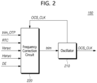
- FIG. 2 is a diagram illustrating the frequency generator according to an embodiment of the present disclosure.
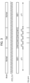
- FIG. 3 is a diagram for describing a frequency measurement period and frequency correction for each mode according to an embodiment of the present disclosure.
- the frequency generator 150 may include an oscillator 210 that generates an oscillator clock signal, and a frequency correction circuit 220 that, in a normal mode, measure the frequency of the oscillator clock signal OCS_CLK during a first frequency measurement period FMT1 with a duration of a first unit period UT1, and in a fast mode according to the state of the oscillator clock signal OCS_CLK, measures the frequency of the oscillator clock signal OCS_CLK during a second frequency measurement period FMT2 with a duration of a second unit period UT2 smaller than the first unit period UT1, and outputs, to the oscillator 210, an adjustment signal trim for correcting a frequency deviation between the measured frequency of the oscillator clock signal OCS_CLK and a target frequency.
- a frequency correction circuit 220 that, in a normal mode, measure the frequency of the oscillator clock signal OCS_CLK during a first frequency measurement period FMT1 with a duration of a first unit period UT1, and in a fast mode according to
- the oscillator 210 may generate the oscillator clock signal OCS_CLK and transmit the generated oscillator clock signal OCS_CLK to the frequency correction circuit 220. In addition, the oscillator 210 may adjust the frequency of the oscillator clock signal OCS_CLK based on the adjustment signal trim output from the frequency correction circuit 220.
- the frequency correction circuit 220 may receive the oscillator clock signal OCS_CLK from the oscillator 210. In addition, the frequency correction circuit 220 may receive the vertical synchronization signal Vsync, the horizontal synchronization signal Hsync, the data enable signal DE, and a real time clock (RTC) signal from the host.
- OCS_CLK oscillator clock signal
- RTC real time clock
- the normal mode is a mode in which the frequency correction circuit 220 measures and corrects the frequency of the oscillator clock signal OCS_CLK during a normal frequency measurement period.
- the frequency measurement period is set to be relatively large, a relatively large number of oscillator clock signals OCS_CLK may be counted, thereby increasing the accuracy of the frequency measurement value.
- the frequency correction circuit 220 measures the oscillator clock signal OCS_CLK during a relatively large frequency measurement period, frequency fluctuations occurring in the oscillator clock signal OCS_CLK may be ignored in terms of average.
- the frequency correction circuit 220 is limited to quickly reflecting frequency fluctuations when correcting the frequency of the oscillator clock signal OCS_CLK during the relatively large frequency measurement period.
- the frequency correction circuit 220 may measure the frequency of the oscillator clock signal OCS_CLK during the second frequency measurement period FMT2 having the duration of the second unit period UT2 smaller than the first unit period UT1.
- the fast mode is a mode in which the frequency of the oscillator clock signal OCS_CLK is corrected by quickly reflecting frequency fluctuations.
- the frequency correction circuit 220 When the frequency correction circuit 220 operates in the normal mode to measure and correct the frequency of the oscillator clock signal OCS_CLK during the relatively large frequency measurement period, a quick response to frequency fluctuations is limited. On the other hand, when the frequency correction circuit 220 operates in the fast mode, the frequency correction circuit 220 measures and corrects the frequency of the oscillator clock signal OCS_CLK during a relatively small frequency measurement period. Accordingly, a quick response to a continuously changing frequency is possible.
- the frequency correction circuit 220 may include a counter (not shown) for measuring the frequency of the oscillator clock signal OCS_CLK.
- the frequency correction circuit 220 may calculate the frequency of the oscillator clock signal OCS_CLK based on the number of toggles of the oscillator clock signal OCS_CLK during the frequency measurement period counted through the counter.
- the first unit period UT1 and the second unit period UT2 may be set in accordance with a policy regarding the operation of the frequency generator.
- the frequency correction circuit 220 may calculate a frequency deviation between the measured frequency of the oscillator clock signal OCS_CLK and the target frequency and may output, to the oscillator 210, the adjustment signal trim for correcting the frequency deviation.
- the oscillator 210 may adjust the frequency of the oscillator clock signal OCS_CLK based on the adjustment signal trim.
- the adjustment signal trim may include a code for increasing or decreasing the frequency of the oscillator clock signal OCS_CLK according to the deviation between the measured frequency of the oscillator clock signal OCS_CLK and the target frequency.
- the frequency correction circuit 220 may receive an initial adjustment signal trim_OTP for outputting the oscillator clock signal OCS_CLK and may transmit the initial adjustment signal trim_OTP to the oscillator 210.
- FIG. 4 is a diagram for describing the first unit period and the second unit period according to an embodiment of the present disclosure.
- the first unit period UT1 may be a period in which a reference clock signal REF input from the outside is toggled by a first count
- the second unit period UT2 may be a period in which the reference clock signal REF is toggled by a second count smaller than the first count
- the reference clock signal REF is a signal used as a reference to determine the frequency measurement period for measuring the frequency of the oscillator clock signal OCS_CLK.
- the reference clock signal REF may be an RTC signal received from the outside.
- the RTC signal may be a signal generated through a crystal oscillator.
- the first count is set to 10, and the first unit period UT1, which is the duration of the first frequency measurement period FMT1, is a period in which the reference clock signal REF is toggled 10 times.
- the frequency correction circuit 220 operating in the normal mode may calculate a frequency by counting the oscillator clock signal OCS_CLK during a period in which the reference clock signal REF is toggled 10 times.
- the second count is set to 2
- the second unit period UT2 which is the duration of the second frequency measurement period FMT2
- the frequency correction circuit 220 operating in the fast mode may calculate a frequency by counting the oscillator clock signal OCS_CLK during a period in which the reference clock signal REF is toggled twice.
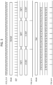
- FIG. 5 is a diagram for describing a frequency correction timing for each mode according to an embodiment of the present disclosure.
- the frequency correction circuit 220 may correct the frequency of the oscillator clock signal OCS_CLK during an interval Int corresponding to one cycle of the reference clock signal REF and then start a new frequency measurement period, and in the fast mode, when a frequency deviation occurs during the second frequency measurement period FMT2, the frequency correction circuit 220 may correct the frequency of the oscillator clock signal OCS_CLK without an interval Int.
- the frequency correction circuit 220 may separately or simultaneously perform the frequency measurement of the oscillator clock signal OCS_CLK and the frequency correction.
- a correction synchronization signal Cal_sync of FIG. 5 is a signal indicating a timing at which correction occurs.
- the first frequency measurement period FMT1 of FIG. 5 may be a period in which the reference clock signal REF is toggled 10 times, and the frequency correction circuit 220 may measure a frequency by counting the oscillator clock signal OCS_CLK during the first frequency measurement period FMT1.
- the frequency correction circuit 220 may output, to the oscillator 210, the adjustment signal trim for correcting the oscillator clock signal OCS_CLK during the interval Int corresponding to one cycle of the reference clock signal REF after the frequency measurement is completed.
- the frequency correction circuit 220 may measure the oscillator clock signal OCS_CLK during the frequency measurement period in which the interval Int is terminated and newly started.
- the interval between the continuous correction synchronization signals Cal_snyc is a period in which a total of 11 reference clock signals REF are toggled, which corresponds to the sum of the interval Int and the duration of the first frequency measurement period FMT1.
- the frequency correction circuit 220 may operate stably in the normal mode by adding the interval Int for frequency correction between the frequency measurement periods and correcting the oscillator clock signal OCS_CLK.
- the second frequency measurement period FMT2 of FIG. 5 may be a period in which the reference clock signal REF is toggled twice, and the frequency correction circuit 220 may measure a frequency by counting the oscillator clock signal OCS_CLK during the second frequency measurement period FMT2.
- the frequency correction circuit 220 may output the adjustment signal trim for correcting the oscillator clock signal OCS_CLK at the same time as the completion of the frequency measurement. That is, the frequency correction circuit 220 may start a new frequency measurement period and measure the oscillator clock signal OCS_CLK,without adding a separate interval Int.
- the frequency correction circuit 220 may quickly respond to frequency fluctuations of the oscillator clock signal OCS_CLK by correcting the oscillator clock signal OCS_CLK without an interval Int.
- FIG. 6 is a diagram for describing switching between respective modes according to an embodiment of the present disclosure.
- the frequency correction circuit 220 may determine the state of the oscillator clock signal OCS_CLK and operate in the normal mode or the fast mode based on the determination result.
- the fast mode may be set for when the frequency of the oscillator clock signal OCS_CLK changes due to a continuous noise effect from the outside.
- the frequency correction circuit 220 may determine whether the state of the oscillator clock signal OCS_CLK is a noise state or a stable state during a certain period.
- the frequency correction circuit 220 operating in the normal mode determines that the state of the oscillator clock signal OCS_CLK is a noise state as long as a TA period, the frequency correction circuit 220 may change from the normal mode to the fast mode and then operate in the fast mode.
- the frequency correction circuit 220 operating in the fast mode determines that the state of the oscillator clock signal OCS_CLK is a stable state as long as a TB period, the frequency correction circuit 220 may change from the fast mode to the normal mode and then operate in the normal mode.
- the frequency correction circuit 220 may operate in the normal mode in a normal case, but may switch to the fast mode and operate in the fast mode, based on the state of the oscillator clock signal OCS_CLK due to a continuous noise effect, or may switch from the fast mode to the normal mode in response thereto and operate in the normal state.
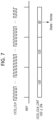
- FIG. 7 is a diagram for describing determination as to the presence or absence of a noise effect according to an embodiment of the present disclosure.
- the frequency correction circuit 220 may determine the state of the oscillator clock signal based on a count value OCS_CLK_CNT of the oscillator clock signal during one cycle of the reference clock signal REF.
- the frequency correction circuit 220 may count the oscillator clock signal OCS_CLK during one cycle of the reference clock signal REF.
- the frequency correction circuit 220 may determine the noise state or the stable state of the oscillator clock signal OCS_CLK according to the presence or absence of the noise injected from the outside, based on the count value OCS_CLK_CNT of the oscillator clock signal, and may determine whether to operate in the normal mode or the fast mode.
- the frequency correction circuit 220 assumes that the oscillator clock signal OCS_CLK is in a noise state.
- the count value OCS_CLK_CNT of the oscillator clock signal during one cycle of the first reference clock signal REF is 100, and the frequency correction circuit may determine that the state of the oscillator clock signal OCS_CLK is not a noise state but a stable state.
- the count value OCS_CLK_CNT of the oscillator clock signal during one cycle of the next reference clock signal REF is 103, and the frequency correction circuit 220 may determine that the state of the oscillator clock signal OCS_CLK is a stable state as before.
- the count value OCS_CLK_CNT of the oscillator clock signal during one cycle of the third reference clock signal REF is 92
- the frequency correction circuit 220 may determine that the state of the oscillator clock signal OCS_CLK is a noise state.
- the frequency correction circuit 220 may determine the normal mode or the fast mode based on the state of the oscillator clock signal OCS_CLK determined during one cycle of the reference clock signal REF by the above-described method.
- FIG. 8 is a diagram for describing an example of a mode according to a flag and the number of occurrence of the flag according to an embodiment of the present disclosure.
- the frequency correction circuit 220 may generate a flag when the state of the oscillator clock signal OCS_CLK is a noise state during one cycle of the reference clock signal REF, and may operate in a fast mode when a flag count Flag_CNT corresponding to the flag is greater than or equal to a third count.
- the frequency correction circuit 220 may change from the normal mode to the fast mode and operate in the fast mode.
- the frequency correction circuit 220 may initialize the flag count Flag_CNT when the flag is not continuous.
- the frequency correction circuit 220 may determine that the state is a noise state and may generate the flag. However, since the oscillator clock signal OCS_CLK is determined to be in a stable state in the subsequent reference clock signal REF, the flag count Flag_CNT may be initialized.
- the frequency correction circuit 220 may change from the normal mode to the fast mode and operate in the fast mode. As the mode is changed, the frequency correction circuit 220 may initialize the flag count Flag_CNT.
- the frequency correction circuit 220 may distinguish between temporary noise and continuous noise and may change to the fast mode and operate in the fast mode only in the case of continuous noise.
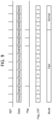
- FIG. 9 is a diagram for describing another example of a mode according to a flag and a flag count according to an embodiment of the present disclosure.
- the frequency correction circuit 220 may generate a flag when the state of the oscillator clock signal OCS_CLK is a stable state during one cycle of the reference clock signal REF, and may operate in a normal mode when a flag count Flag_CNT corresponding to the flag is greater than or equal to a fourth count.
- the frequency correction circuit 220 may change from the fast mode to the normal mode and operate in the normal mode.
- the frequency correction circuit 220 may initialize the flag count Flag_CNT when the flag is not continuous by the fourth count.
- the frequency correction circuit 220 may determine that the state is a stable state and may generate the flag. However, since the oscillator clock signal OCS_CLK is determined to be in a noise state in the subsequent reference clock signal REF, the flag count Flag_CNT may be initialized.
- the frequency correction circuit 220 may change from the fast mode to the normal mode and operate in the normal mode. As the mode is changed, the frequency correction circuit 220 may initialize the flag count Flag_CNT.
- the frequency correction circuit 220 may distinguish between a temporary stable state and a continuous stable state and may change to the normal mode and operate in the normal mode only when the continuous stable state is maintained.
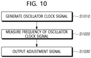
- FIG. 10 is a diagram illustrating a frequency correction method for a frequency generator according to another embodiment of the present disclosure.
- the frequency correction method for the frequency generator 150 may include operation S1010 of generating the oscillator clock signal OCS_CLK.
- the frequency correction method for the frequency generator 150 may include operation S1020 of measuring the frequency of the oscillator clock signal OCS_CLK in either the normal mode corresponding to the first frequency measurement period with the duration of the first unit period or the fast mode corresponding to the second frequency measurement period with the duration of the second unit period smaller than the first unit period.
- the first unit period may be a period in which the reference clock signal is toggled by the first count
- the second unit period may be a period in which the reference clock signal is toggled by the second count smaller than the first count
- the frequency correction method for the frequency generator 150 may include operation S1030 of outputting the adjustment signal for correcting the frequency deviation between the measured frequency of the oscillator clock signal OCS_CLK and the target frequency.
- the adjustment signal trim for correcting the frequency of the oscillator clock signal OCS_CLK may be output during the interval Int corresponding to one cycle of the reference clock signal REF, and in the fast mode, the adjustment signal trim for correcting the frequency of the oscillator clock signal OCS_CLK may be output without an interval Int.
- the frequency correction method for the frequency generator 150 may further include operation of determining the state of the oscillator clock signal OCS_CLK and may determine the normal mode or the fast mode based on the determination result.
- the frequency correction method for the frequency generator 150 may count the count value OCS_CLK_CNT of the oscillator clock signal during one cycle of the reference clock signal REF and determine the state of the oscillator clock signal OCS_CLK based on the count value OCS_CLK_CNT of the oscillator clock signal.
- the frequency correction method for the frequency generator 150 may further include operation of generating the flag when the state of the oscillator clock signal OCS_CLK is the noise state in the normal mode, and operation of changing to the fast mode when the flag count Flag_CNT corresponding to the flag is greater than or equal to the third count.
- the frequency correction method for the frequency generator may initialize the flag count Flag_CNT when the flag is not continuous.
- the frequency correction method for the frequency generator 150 may further include operation of generating the flag when the state of the oscillator clock signal OCS_CLK is the stable state in the fast mode, and operation of changing to the fast mode when the flag count Flag_CNT corresponding to the flag is greater than or equal to the fourth count.
- the frequency correction method for the frequency generator may initialize the flag count Flag_CNT when the flag is not continuous.
Landscapes
- Engineering & Computer Science (AREA)
- Theoretical Computer Science (AREA)
- Physics & Mathematics (AREA)
- General Engineering & Computer Science (AREA)
- General Physics & Mathematics (AREA)
- Stabilization Of Oscillater, Synchronisation, Frequency Synthesizers (AREA)
- Manipulation Of Pulses (AREA)
Abstract
Description
- The present embodiment relates to a frequency generator for correcting frequency fluctuations of an oscillator and a frequency correction method for the frequency generator.
- As information technology develops, the market for display devices, which are a medium for connecting users and information, is growing. Accordingly, the use of display devices such as organic light emitting displays (OLEDs) is increasing.
- Such display devices may include a display panel and a display driving circuit that drives the display panel.
- In general, the display driving circuit may operate according to a refresh rate, and the refresh rate may be maintained by an oscillator clock signal of a frequency generator included in the display driving circuit.
- The frequency of the clock signal may change depending on factors such as the process, voltage, or temperature of an oscillator. When the frequency of the clock signal changes, the image quality of the display device may deteriorate.
- Therefore, the display driving circuit has to periodically check and correct frequency fluctuations of the clock signal so as to quickly improve image quality degradation.
- Here, the display driving circuit may receive image data from a host such as an application processor (AP), a central processing unit (CPU), or a graphics processing unit (GPU) included in the display device and may receive, from the host, a vertical synchronization signal, a horizontal synchronization signal, and a data enable signal for displaying the image data on the display panel.
- Conventionally, a frequency generator measures a frequency of a clock signal of an oscillator while a reference clock signal of a certain period is repeated a certain number of times, and compensates for frequency fluctuations of the clock signal by comparing the measured frequency of the clock signal with a target frequency.
- However, when the frequency of the clock signal is continuously affected by external factors such as wireless charging, the display driving circuit may not actively cope with the frequency fluctuations because the time required to correct the frequency change of the clock signal is constant.
- Against this background, an object of the present embodiment is to provide a frequency correction technology that actively responds to continuous frequency fluctuations of a clock signal through a frequency measurement period of at least two unit periods.
- To achieve the above-described obj ects, in an aspect, the present embodiment provides a frequency generator including: an oscillator that generates an oscillator clock signal; and a frequency correction circuit that selectively operates in one of a normal mode and a fast mode with different correction periods according to a state of the oscillator clock signal.
- The frequency generator may measure a frequency of the oscillator clock signal during a first period in the normal mode, may measure the frequency of the oscillator clock signal during a second period shorter than the first period in the fast mode, and may output, to the oscillator, an adjustment signal for correcting a frequency deviation between the measured frequency of the oscillator clock signal and a target frequency.
- When the frequency deviation occurs in the normal mode, the frequency correction circuit may correct the frequency of the oscillator clock signal during a preset interval and then start measuring a new frequency, and when the frequency deviation occurs in the fast mode, the frequency correction circuit may correct the frequency of the oscillator clock signal without the interval.
- The first period may be a period in which a reference clock signal input from an outside is toggled by a first count, and the second period may be a period in which the reference clock signal is toggled by a second count smaller than the first count.
- In another aspect, the present embodiment provides a frequency correction method for correcting a frequency of an oscillator in a frequency generator, the frequency correction method including: generating an oscillator clock signal; and measuring a frequency of the oscillator clock signal in one of a normal mode and a fast mode with different correction periods according to a state of the oscillator clock signal.
- In the method, the measuring of the frequency of the oscillator clock signal may include measuring the frequency of the oscillator clock signal during a first period in the normal mode, and measuring the frequency of the oscillator clock signal during a second period shorter than the first period in the fast mode.
- The method may further include outputting an adjustment signal for correcting a frequency deviation between the measured frequency of the oscillator clock signal and a target frequency, wherein the outputting of the adjustment signal may include outputting the adjustment signal for correcting the frequency of the oscillator clock signal during a preset interval in the normal mode, and outputting the adjustment signal for correcting the frequency of the oscillator clock signal without the interval in the fast mode.
- As described above, according to the present embodiment, a frequency generator, which actively responds to continuous frequency fluctuations of a clock signal through a frequency measurement period of at least two unit periods, and a frequency correction method for the frequency generator may be provided.
-
-
FIG. 1 is a configuration diagram of a display device according to an embodiment of the present disclosure. -
FIG. 2 is a diagram illustrating a frequency generator according to an embodiment of the present disclosure. -
FIG. 3 is a diagram for describing a frequency measurement period and frequency correction for each mode according to an embodiment of the present disclosure. -
FIG. 4 is a diagram for describing a first unit period and a second unit period according to an embodiment of the present disclosure. -
FIG. 5 is a diagram for describing a frequency correction timing for each mode according to an embodiment of the present disclosure. -
FIG. 6 is a diagram for describing switching between respective modes according to an embodiment of the present disclosure. -
FIG. 7 is a diagram for describing determination as to the presence or absence of a noise effect according to an embodiment of the present disclosure. -
FIG. 8 is a diagram for describing an example of a mode according to a flag and a flag count according to an embodiment of the present disclosure. -
FIG. 9 is a diagram for describing another example of a mode according to a flag and a flag count according to an embodiment of the present disclosure. -
FIG. 10 is a diagram illustrating a frequency correction method for a frequency generator according to another embodiment of the present disclosure. - Hereinafter, embodiments of the present disclosure will be described in detail with reference to exemplary drawings.
-
FIG. 1 is a configuration diagram of a display device according to an embodiment of the present disclosure. - Referring to
FIG. 1 , adisplay device 100 may include adisplay panel 110 and a display driving circuit that drives thedisplay panel 110. - A plurality of data lines DL and a plurality of gate lines GL may be arranged on the
display panel 110, and a plurality of pixels P may be arranged on thedisplay panel 110. Here, the plurality of pixels P may be arranged in a matrix form including a plurality of horizontal lines and a plurality of vertical lines. - The display driving circuit that drives the
display panel 110 may include asource driver 120, agate driver 130, atiming controller 140, and afrequency generator 150. - In the display driving circuit, the
gate driver 130 may output a scan signal of a turn-on voltage or a turn-off voltage to the gate line GL. When the scan signal of the turn-on voltage is supplied to the pixel P, the pixel P is connected to the data line DL, and when the scan signal of the turn-off voltage is supplied to the pixel P, the pixel P and the data line DL are disconnected from each other. - In the display driving circuit, the
source driver 120 supplies a data voltage to the data line DL. The data voltage supplied to the data line DL is transmitted to the pixel P connected to the data line DL according to the scan signal. - In the display driving circuit, the
timing controller 140 may receive a vertical synchronization signal Vsync, a horizontal synchronization signal Hsync, a data enable signal DE, and image data RGB from thehost 10. Thetiming controller 140 may receive an oscillator clock signal OCS_CLK from thefrequency generator 150. - Meanwhile, the
timing controller 140 may generate a control signal of thegate driver 130 and a control signal of thesource driver 120 by using the vertical synchronization signal Vsync, the horizontal synchronization signal Hsync, the data enable signal DE, and the oscillator clock signal OCS_CLK. - First, the
timing controller 140 may generate a gate control signal GCS by using the vertical synchronization signal Vsync, the horizontal synchronization signal Hsync, the data enable signal DE, and the oscillator clock signal OCS_CLK and may output the gate control signal to thegate driver 130. Here, the gate control signal GCS may include a gate start pulse (GSP), a gate shift clock (GSC), a gate output enable signal (GOE), and a gate modulation control signal. - The
timing controller 140 may convert the image data RGB received from thehost 10 into a data format to be used in thesource driver 120. - The
timing controller 140 may output the converted image data RGB' to thesource driver 120. - In addition, the
timing controller 140 may generate a data control signal DCS by using the vertical synchronization signal Vsync, the horizontal synchronization signal Hsync, the data enable signal DE, and the oscillator clock signal OCS_CLK and may output the data control signal to thesource driver 120. - Here, the data control signal DCS may include a source start pulse (SSP), a source shift clock (SSC), and a source output enable (SOE) signal.
- The
frequency generator 150 may include an oscillator that outputs the oscillator clock signal OCS_CLK. The oscillator clock signal OCS_CLK may be transmitted to thetiming controller 140. -
FIG. 2 is a diagram illustrating the frequency generator according to an embodiment of the present disclosure. -
FIG. 3 is a diagram for describing a frequency measurement period and frequency correction for each mode according to an embodiment of the present disclosure. - Referring to
FIGS. 2 and3 , thefrequency generator 150 may include anoscillator 210 that generates an oscillator clock signal, and afrequency correction circuit 220 that, in a normal mode, measure the frequency of the oscillator clock signal OCS_CLK during a first frequency measurement period FMT1 with a duration of a first unit period UT1, and in a fast mode according to the state of the oscillator clock signal OCS_CLK, measures the frequency of the oscillator clock signal OCS_CLK during a second frequency measurement period FMT2 with a duration of a second unit period UT2 smaller than the first unit period UT1, and outputs, to theoscillator 210, an adjustment signal trim for correcting a frequency deviation between the measured frequency of the oscillator clock signal OCS_CLK and a target frequency. - The
oscillator 210 may generate the oscillator clock signal OCS_CLK and transmit the generated oscillator clock signal OCS_CLK to thefrequency correction circuit 220. In addition, theoscillator 210 may adjust the frequency of the oscillator clock signal OCS_CLK based on the adjustment signal trim output from thefrequency correction circuit 220. - The
frequency correction circuit 220 may receive the oscillator clock signal OCS_CLK from theoscillator 210. In addition, thefrequency correction circuit 220 may receive the vertical synchronization signal Vsync, the horizontal synchronization signal Hsync, the data enable signal DE, and a real time clock (RTC) signal from the host. - The normal mode is a mode in which the
frequency correction circuit 220 measures and corrects the frequency of the oscillator clock signal OCS_CLK during a normal frequency measurement period. When the frequency measurement period is set to be relatively large, a relatively large number of oscillator clock signals OCS_CLK may be counted, thereby increasing the accuracy of the frequency measurement value. In addition, when thefrequency correction circuit 220 measures the oscillator clock signal OCS_CLK during a relatively large frequency measurement period, frequency fluctuations occurring in the oscillator clock signal OCS_CLK may be ignored in terms of average. - However, when continuous frequency fluctuations occur in the oscillator clock signal OCS_CLK,the
frequency correction circuit 220 is limited to quickly reflecting frequency fluctuations when correcting the frequency of the oscillator clock signal OCS_CLK during the relatively large frequency measurement period. - Meanwhile, as described above, in the fast mode, the
frequency correction circuit 220 may measure the frequency of the oscillator clock signal OCS_CLK during the second frequency measurement period FMT2 having the duration of the second unit period UT2 smaller than the first unit period UT1. - The fast mode is a mode in which the frequency of the oscillator clock signal OCS_CLK is corrected by quickly reflecting frequency fluctuations.
- When the
frequency correction circuit 220 operates in the normal mode to measure and correct the frequency of the oscillator clock signal OCS_CLK during the relatively large frequency measurement period, a quick response to frequency fluctuations is limited. On the other hand, when thefrequency correction circuit 220 operates in the fast mode, thefrequency correction circuit 220 measures and corrects the frequency of the oscillator clock signal OCS_CLK during a relatively small frequency measurement period. Accordingly, a quick response to a continuously changing frequency is possible. - Meanwhile, the
frequency correction circuit 220 may include a counter (not shown) for measuring the frequency of the oscillator clock signal OCS_CLK. Thefrequency correction circuit 220 may calculate the frequency of the oscillator clock signal OCS_CLK based on the number of toggles of the oscillator clock signal OCS_CLK during the frequency measurement period counted through the counter. - The first unit period UT1 and the second unit period UT2 may be set in accordance with a policy regarding the operation of the frequency generator.
- The
frequency correction circuit 220 may calculate a frequency deviation between the measured frequency of the oscillator clock signal OCS_CLK and the target frequency and may output, to theoscillator 210, the adjustment signal trim for correcting the frequency deviation. - In this case, as described above, the
oscillator 210 may adjust the frequency of the oscillator clock signal OCS_CLK based on the adjustment signal trim. The adjustment signal trim may include a code for increasing or decreasing the frequency of the oscillator clock signal OCS_CLK according to the deviation between the measured frequency of the oscillator clock signal OCS_CLK and the target frequency. - Meanwhile, when the
oscillator 210 is initially driven, thefrequency correction circuit 220 may receive an initial adjustment signal trim_OTP for outputting the oscillator clock signal OCS_CLK and may transmit the initial adjustment signal trim_OTP to theoscillator 210. -
FIG. 4 is a diagram for describing the first unit period and the second unit period according to an embodiment of the present disclosure. - Referring to
FIG. 4 , the first unit period UT1 may be a period in which a reference clock signal REF input from the outside is toggled by a first count, and the second unit period UT2 may be a period in which the reference clock signal REF is toggled by a second count smaller than the first count. - The reference clock signal REF is a signal used as a reference to determine the frequency measurement period for measuring the frequency of the oscillator clock signal OCS_CLK. The reference clock signal REF may be an RTC signal received from the outside. In this case, the RTC signal may be a signal generated through a crystal oscillator.
- As illustrated in
FIG. 4 , the first count is set to 10, and the first unit period UT1, which is the duration of the first frequency measurement period FMT1, is a period in which the reference clock signal REF is toggled 10 times. Thefrequency correction circuit 220 operating in the normal mode may calculate a frequency by counting the oscillator clock signal OCS_CLK during a period in which the reference clock signal REF is toggled 10 times. - In addition, as illustrated in
FIG. 4 , the second count is set to 2, and the second unit period UT2, which is the duration of the second frequency measurement period FMT2, is a period in which the reference clock signal REF is toggled twice. Thefrequency correction circuit 220 operating in the fast mode may calculate a frequency by counting the oscillator clock signal OCS_CLK during a period in which the reference clock signal REF is toggled twice. -
FIG. 5 is a diagram for describing a frequency correction timing for each mode according to an embodiment of the present disclosure. - Referring to
FIG. 5 , in the normal mode, when a frequency deviation occurs during the first frequency measurement period FMT1, thefrequency correction circuit 220 may correct the frequency of the oscillator clock signal OCS_CLK during an interval Int corresponding to one cycle of the reference clock signal REF and then start a new frequency measurement period, and in the fast mode, when a frequency deviation occurs during the second frequency measurement period FMT2, thefrequency correction circuit 220 may correct the frequency of the oscillator clock signal OCS_CLK without an interval Int. - The
frequency correction circuit 220 may separately or simultaneously perform the frequency measurement of the oscillator clock signal OCS_CLK and the frequency correction. - A correction synchronization signal Cal_sync of
FIG. 5 is a signal indicating a timing at which correction occurs. - The first frequency measurement period FMT1 of
FIG. 5 may be a period in which the reference clock signal REF is toggled 10 times, and thefrequency correction circuit 220 may measure a frequency by counting the oscillator clock signal OCS_CLK during the first frequency measurement period FMT1. In the normal mode, when the deviation occurs between the measured frequency of the oscillator clock signal OCS_CLK and the target frequency and thus the frequency correction is required, thefrequency correction circuit 220 may output, to theoscillator 210, the adjustment signal trim for correcting the oscillator clock signal OCS_CLK during the interval Int corresponding to one cycle of the reference clock signal REF after the frequency measurement is completed. Thefrequency correction circuit 220 may measure the oscillator clock signal OCS_CLK during the frequency measurement period in which the interval Int is terminated and newly started. - In
FIG. 5 , in the normal mode, the interval between the continuous correction synchronization signals Cal_snyc is a period in which a total of 11 reference clock signals REF are toggled, which corresponds to the sum of the interval Int and the duration of the first frequency measurement period FMT1. - The
frequency correction circuit 220 may operate stably in the normal mode by adding the interval Int for frequency correction between the frequency measurement periods and correcting the oscillator clock signal OCS_CLK. - Meanwhile, the second frequency measurement period FMT2 of
FIG. 5 may be a period in which the reference clock signal REF is toggled twice, and thefrequency correction circuit 220 may measure a frequency by counting the oscillator clock signal OCS_CLK during the second frequency measurement period FMT2. In the fast mode, when the correction is required due to the deviation between the measured frequency of the oscillator clock signal OCS_CLK and the target frequency, thefrequency correction circuit 220 may output the adjustment signal trim for correcting the oscillator clock signal OCS_CLK at the same time as the completion of the frequency measurement. That is, thefrequency correction circuit 220 may start a new frequency measurement period and measure the oscillator clock signal OCS_CLK,without adding a separate interval Int. - In the fast mode, the
frequency correction circuit 220 may quickly respond to frequency fluctuations of the oscillator clock signal OCS_CLK by correcting the oscillator clock signal OCS_CLK without an interval Int. -
FIG. 6 is a diagram for describing switching between respective modes according to an embodiment of the present disclosure. - Referring to
FIG. 6 , thefrequency correction circuit 220 may determine the state of the oscillator clock signal OCS_CLK and operate in the normal mode or the fast mode based on the determination result. - The fast mode may be set for when the frequency of the oscillator clock signal OCS_CLK changes due to a continuous noise effect from the outside. In order to determine either the normal mode or the fast mode, the
frequency correction circuit 220 may determine whether the state of the oscillator clock signal OCS_CLK is a noise state or a stable state during a certain period. - In
FIG. 6 , when thefrequency correction circuit 220 operating in the normal mode determines that the state of the oscillator clock signal OCS_CLK is a noise state as long as a TA period, thefrequency correction circuit 220 may change from the normal mode to the fast mode and then operate in the fast mode. - Meanwhile, when the
frequency correction circuit 220 operating in the fast mode determines that the state of the oscillator clock signal OCS_CLK is a stable state as long as a TB period, thefrequency correction circuit 220 may change from the fast mode to the normal mode and then operate in the normal mode. - In this manner, the
frequency correction circuit 220 may operate in the normal mode in a normal case, but may switch to the fast mode and operate in the fast mode, based on the state of the oscillator clock signal OCS_CLK due to a continuous noise effect, or may switch from the fast mode to the normal mode in response thereto and operate in the normal state. -
FIG. 7 is a diagram for describing determination as to the presence or absence of a noise effect according to an embodiment of the present disclosure. - Referring to
FIG. 7 , thefrequency correction circuit 220 may determine the state of the oscillator clock signal based on a count value OCS_CLK_CNT of the oscillator clock signal during one cycle of the reference clock signal REF. - Apart from counting the oscillator clock signal OCS_CLK for measuring the frequency during the first frequency measurement period or the second frequency measurement period, the
frequency correction circuit 220 may count the oscillator clock signal OCS_CLK during one cycle of the reference clock signal REF. Thefrequency correction circuit 220 may determine the noise state or the stable state of the oscillator clock signal OCS_CLK according to the presence or absence of the noise injected from the outside, based on the count value OCS_CLK_CNT of the oscillator clock signal, and may determine whether to operate in the normal mode or the fast mode. - For example, when the count value OCS_CLK_CNT of the oscillator clock signal per cycle of the reference clock signal REF corresponding to the target frequency is 100 and is less than 5% or more than 5%, the
frequency correction circuit 220 assumes that the oscillator clock signal OCS_CLK is in a noise state. - In
FIG. 7 , the count value OCS_CLK_CNT of the oscillator clock signal during one cycle of the first reference clock signal REF is 100, and the frequency correction circuit may determine that the state of the oscillator clock signal OCS_CLK is not a noise state but a stable state. - The count value OCS_CLK_CNT of the oscillator clock signal during one cycle of the next reference clock signal REF is 103, and the
frequency correction circuit 220 may determine that the state of the oscillator clock signal OCS_CLK is a stable state as before. - Meanwhile, the count value OCS_CLK_CNT of the oscillator clock signal during one cycle of the third reference clock signal REF is 92, and the
frequency correction circuit 220 may determine that the state of the oscillator clock signal OCS_CLK is a noise state. - The
frequency correction circuit 220 may determine the normal mode or the fast mode based on the state of the oscillator clock signal OCS_CLK determined during one cycle of the reference clock signal REF by the above-described method. -
FIG. 8 is a diagram for describing an example of a mode according to a flag and the number of occurrence of the flag according to an embodiment of the present disclosure. - Referring to
FIG. 8 , in a normal mode, thefrequency correction circuit 220 may generate a flag when the state of the oscillator clock signal OCS_CLK is a noise state during one cycle of the reference clock signal REF, and may operate in a fast mode when a flag count Flag_CNT corresponding to the flag is greater than or equal to a third count. - For example, when the third count is set to 3 and the state of the oscillator clock signal OCS_CLK is a noise state during three continuous or intermittent cycles of the reference clock signal REF, the
frequency correction circuit 220 may change from the normal mode to the fast mode and operate in the fast mode. - Meanwhile, the
frequency correction circuit 220 may initialize the flag count Flag_CNT when the flag is not continuous. - In
FIG. 8 , when it is assumed that frequency fluctuations occur in a portion of the oscillator clock signal OCS_CLK in a stable state corresponding to the cycle of the third reference clock signal REF, thefrequency correction circuit 220 may determine that the state is a noise state and may generate the flag. However, since the oscillator clock signal OCS_CLK is determined to be in a stable state in the subsequent reference clock signal REF, the flag count Flag_CNT may be initialized. - Thereafter, when the flag occurs three times in succession in the seventh to ninth times of the reference clock signal REF, the
frequency correction circuit 220 may change from the normal mode to the fast mode and operate in the fast mode. As the mode is changed, thefrequency correction circuit 220 may initialize the flag count Flag_CNT. - Accordingly, the
frequency correction circuit 220 may distinguish between temporary noise and continuous noise and may change to the fast mode and operate in the fast mode only in the case of continuous noise. -
FIG. 9 is a diagram for describing another example of a mode according to a flag and a flag count according to an embodiment of the present disclosure. - Referring to
FIG. 9 , in a fast mode, thefrequency correction circuit 220 may generate a flag when the state of the oscillator clock signal OCS_CLK is a stable state during one cycle of the reference clock signal REF, and may operate in a normal mode when a flag count Flag_CNT corresponding to the flag is greater than or equal to a fourth count. - For example, when the fourth count is set to 3 and the state of the oscillator clock signal OCS_CLK is a stable state during three continuous or intermittent cycles of the reference clock signal REF, the
frequency correction circuit 220 may change from the fast mode to the normal mode and operate in the normal mode. - Meanwhile, the
frequency correction circuit 220 may initialize the flag count Flag_CNT when the flag is not continuous by the fourth count. - In
FIG. 9 , when it is assumed that frequency fluctuations do not occur in a portion of the oscillator clock signal OCS_CLK in a noise state corresponding to the cycle of the second reference clock signal REF, thefrequency correction circuit 220 may determine that the state is a stable state and may generate the flag. However, since the oscillator clock signal OCS_CLK is determined to be in a noise state in the subsequent reference clock signal REF, the flag count Flag_CNT may be initialized. - Thereafter, when the flag occurs three times in succession in the seventh to ninth times of the reference clock signal REF, the
frequency correction circuit 220 may change from the fast mode to the normal mode and operate in the normal mode. As the mode is changed, thefrequency correction circuit 220 may initialize the flag count Flag_CNT. - Accordingly, the
frequency correction circuit 220 may distinguish between a temporary stable state and a continuous stable state and may change to the normal mode and operate in the normal mode only when the continuous stable state is maintained. -
FIG. 10 is a diagram illustrating a frequency correction method for a frequency generator according to another embodiment of the present disclosure. - Referring to
FIG. 10 , the frequency correction method for thefrequency generator 150 may include operation S1010 of generating the oscillator clock signal OCS_CLK. - In addition, the frequency correction method for the
frequency generator 150 may include operation S1020 of measuring the frequency of the oscillator clock signal OCS_CLK in either the normal mode corresponding to the first frequency measurement period with the duration of the first unit period or the fast mode corresponding to the second frequency measurement period with the duration of the second unit period smaller than the first unit period. - In this case, the first unit period may be a period in which the reference clock signal is toggled by the first count, and the second unit period may be a period in which the reference clock signal is toggled by the second count smaller than the first count.
- In addition, the frequency correction method for the
frequency generator 150 may include operation S1030 of outputting the adjustment signal for correcting the frequency deviation between the measured frequency of the oscillator clock signal OCS_CLK and the target frequency. - In this case, in operation S 1030 of outputting the adjustment signal, in the normal mode, the adjustment signal trim for correcting the frequency of the oscillator clock signal OCS_CLK may be output during the interval Int corresponding to one cycle of the reference clock signal REF, and in the fast mode, the adjustment signal trim for correcting the frequency of the oscillator clock signal OCS_CLK may be output without an interval Int.
- Meanwhile, the frequency correction method for the
frequency generator 150 may further include operation of determining the state of the oscillator clock signal OCS_CLK and may determine the normal mode or the fast mode based on the determination result. - Meanwhile, in operation of determining the state of the oscillator clock signal, the frequency correction method for the
frequency generator 150 may count the count value OCS_CLK_CNT of the oscillator clock signal during one cycle of the reference clock signal REF and determine the state of the oscillator clock signal OCS_CLK based on the count value OCS_CLK_CNT of the oscillator clock signal. - In this case, the frequency correction method for the
frequency generator 150 may further include operation of generating the flag when the state of the oscillator clock signal OCS_CLK is the noise state in the normal mode, and operation of changing to the fast mode when the flag count Flag_CNT corresponding to the flag is greater than or equal to the third count. - In this case, the frequency correction method for the frequency generator may initialize the flag count Flag_CNT when the flag is not continuous.
- Meanwhile, the frequency correction method for the
frequency generator 150 may further include operation of generating the flag when the state of the oscillator clock signal OCS_CLK is the stable state in the fast mode, and operation of changing to the fast mode when the flag count Flag_CNT corresponding to the flag is greater than or equal to the fourth count. - In this case, the frequency correction method for the frequency generator may initialize the flag count Flag_CNT when the flag is not continuous.
Claims (18)
- A frequency generator comprising:an oscillator that generates an oscillator clock signal; anda frequency correction circuit that selectively operates in one of a normal mode and a fast mode with different correction periods according to a state of theoscillator clock signal.
- The frequency generator of claim 1, wherein the frequency generator measures a frequency of the oscillator clock signal during a first period in the normal mode, measure the frequency of the oscillator clock signal during a second period shorter than the first period in the fast mode, and outputs, to the oscillator, an adjustment signal for correcting a frequency deviation between the measured frequency of the oscillator clock signal and a target frequency.
- The frequency generator of claim 2, wherein, when the frequency deviation occurs in the normal mode, the frequency correction circuit corrects the frequency of the oscillator clock signal during a preset interval and then starts measuring a new frequency, and when the frequency deviation occurs in the fast mode, the frequency correction circuit corrects the frequency of the oscillator clock signal without the interval.
- The frequency generator of claim 2, wherein the first period is a period in which a reference clock signal input from an outside is toggled by a first count, and
the second period is a period in which the reference clock signal is toggled by a second count smaller than the first count. - The frequency generator of claim 4, wherein the frequency correction circuit determines the state of the oscillator clock signal based on a count value of the oscillator clock signal during one cycle of the reference clock signal.
- The frequency generator of claim 5, wherein the frequency correction circuit generates a flag when the state of the oscillator clock signal during one cycle of the reference clock signal is a noise state in the normal mode, and operates in the fast mode when a flag count corresponding to the flag is greater than or equal to a third count.
- The frequency generator of claim 6, wherein the frequency correction circuit initializes the flag count when the flag is not continuous.
- The frequency generator of claim 5, wherein the frequency correction circuit generates a flag when the state of the oscillator clock signal during one cycle of the reference clock signal is a stable state in the fast mode, and operates in the normal mode when a flag count corresponding to the flag is greater than or equal to a fourth count.
- The frequency generator of claim 8, wherein the frequency correction circuit initializes the flag count when the flag is not continuous.
- A frequency correction method for correcting a frequency of an oscillator in a frequency generator, the frequency correction method comprising:generating an oscillator clock signal; andmeasuring a frequency of the oscillator clock signal in one of a normal mode and a fast mode with different correction periods according to a state of the oscillator clock signal.
- The frequency correction method of claim 10, wherein the measuring of the frequency of the oscillator clock signal comprises measuring the frequency of the oscillator clock signal during a first period in the normal mode, and measuring the frequency of the oscillator clock signal during a second period shorter than the first period in the fast mode.
- The frequency correction method of claim 11, further comprising outputting an adjustment signal for correcting a frequency deviation between the measured frequency of the oscillator clock signal and a target frequency, wherein the outputting of the adjustment signal comprises outputting the adjustment signal for correcting the frequency of the oscillator clock signal during a preset interval in the normal mode, and outputting the adjustment signal for correcting the frequency of the oscillator clock signal without the interval in the fast mode.
- The frequency correction method of claim 12, further comprising determining the state of the oscillator clock signal, wherein the normal mode or the fast mode is determined based on the determination result.
- The frequency correction method of claim 13, wherein the first period is a period in which a reference clock signal input from an outside is toggled by a first count,the second period is a period in which the reference clock signal is toggled by a second count smaller than the first count, andthe determining of the state of the oscillator clock signal comprises counting a count value of the oscillator clock signal during one cycle of the reference clock signal, and determining the state of the oscillator clock signal based on the count value of the oscillator clock signal.
- The frequency correction method of claim 14, further comprising:generating a flag in the normal mode when the state of the oscillator clock signal is a noise state; andchanging to the fast mode when a flag count corresponding to the flag is greater than or equal to a third count.
- The frequency correction method of claim 15, wherein the flag count is initialized when the flag is not continuous.
- The frequency correction method of claim 14, further comprising:generating a flag in the fast mode when the state of the oscillator clock signal is stable; andchanging to the normal mode when a flag count corresponding to the flag is greater than or equal to a fourth count.
- The frequency correction method of claim 17, wherein the flag count is initialized when the flag is not continuous.
Applications Claiming Priority (2)
| Application Number | Priority Date | Filing Date | Title |
|---|---|---|---|
| KR1020210183841A KR20230094575A (en) | 2021-12-21 | 2021-12-21 | Frequency generator and frequency correction method of frequency generator |
| PCT/KR2022/020445 WO2023121140A1 (en) | 2021-12-21 | 2022-12-15 | Frequency generator and frequency correction method for frequency generator |
Publications (2)
| Publication Number | Publication Date |
|---|---|
| EP4456423A1 true EP4456423A1 (en) | 2024-10-30 |
| EP4456423A4 EP4456423A4 (en) | 2025-11-12 |
Family
ID=86903335
Family Applications (1)
| Application Number | Title | Priority Date | Filing Date |
|---|---|---|---|
| EP22911773.4A Pending EP4456423A4 (en) | 2021-12-21 | 2022-12-15 | FREQUENCY GENERATOR AND FREQUENCY CORRECTION METHOD FOR THE FREQUENCY GENERATOR |
Country Status (5)
| Country | Link |
|---|---|
| US (1) | US12671394B2 (en) |
| EP (1) | EP4456423A4 (en) |
| KR (1) | KR20230094575A (en) |
| CN (1) | CN118414787A (en) |
| WO (1) | WO2023121140A1 (en) |
Families Citing this family (1)
| Publication number | Priority date | Publication date | Assignee | Title |
|---|---|---|---|---|
| CN121565088A (en) * | 2026-01-14 | 2026-02-24 | 京东方科技集团股份有限公司 | Display driving method, display driver, display device, and computer storage medium |
Family Cites Families (13)
| Publication number | Priority date | Publication date | Assignee | Title |
|---|---|---|---|---|
| JP2003219202A (en) * | 2002-01-24 | 2003-07-31 | Matsushita Electric Ind Co Ltd | Image distortion correction apparatus and image distortion correction method |
| KR20050035587A (en) | 2003-10-13 | 2005-04-19 | 매그나칩 반도체 유한회사 | Frequency calibration apparatus of low power osicllator of bluetooth and method the same |
| JP4365297B2 (en) * | 2004-09-15 | 2009-11-18 | 株式会社リコー | Image forming apparatus and image forming method |
| JP2008015006A (en) * | 2006-07-03 | 2008-01-24 | Nec Electronics Corp | Display controller, display device, and display data transfer method |
| US7420428B2 (en) * | 2006-07-13 | 2008-09-02 | Itt Manufacturing Enterprises, Inc. | Low noise phase locked loop with a high precision lock detector |
| US8085247B2 (en) | 2007-01-03 | 2011-12-27 | Apple Inc. | Advanced frequency calibration |
| US7898343B1 (en) * | 2007-12-21 | 2011-03-01 | Rf Micro Devices, Inc. | Frequency-locked loop calibration of a phase-locked loop gain |
| US7881895B2 (en) | 2008-05-27 | 2011-02-01 | Sony Ericsson Mobile Communications Ab | Methods of calibrating a clock using multiple clock periods with a single counter and related devices and methods |
| TWI424305B (en) * | 2010-04-08 | 2014-01-21 | Via Telecom Co Ltd | Clock generators and generating methods, and mobile communication devices |
| KR101891563B1 (en) | 2012-05-29 | 2018-08-24 | 엘지디스플레이 주식회사 | Integrated circuit with frequency calibration function and frequency calibration method using it |
| KR102071573B1 (en) | 2013-06-13 | 2020-03-02 | 삼성전자주식회사 | Display driver ic for controlling a frequency of an oscillator using an external clock signal, device having the same, and methods thereof |
| US10355679B2 (en) | 2017-12-01 | 2019-07-16 | Novatek Microelectronics Corp. | Display driving circuit, calibration module, and associated calibration method |
| GB201918967D0 (en) * | 2019-12-20 | 2020-02-05 | Nordic Semiconductor Asa | Clock circuit portions |
-
2021
- 2021-12-21 KR KR1020210183841A patent/KR20230094575A/en active Pending
-
2022
- 2022-12-15 US US18/722,380 patent/US12671394B2/en active Active
- 2022-12-15 EP EP22911773.4A patent/EP4456423A4/en active Pending
- 2022-12-15 WO PCT/KR2022/020445 patent/WO2023121140A1/en not_active Ceased
- 2022-12-15 CN CN202280084126.4A patent/CN118414787A/en active Pending
Also Published As
| Publication number | Publication date |
|---|---|
| WO2023121140A1 (en) | 2023-06-29 |
| CN118414787A (en) | 2024-07-30 |
| US12671394B2 (en) | 2026-06-30 |
| US20240421802A1 (en) | 2024-12-19 |
| EP4456423A4 (en) | 2025-11-12 |
| KR20230094575A (en) | 2023-06-28 |
Similar Documents
| Publication | Publication Date | Title |
|---|---|---|
| US11694598B2 (en) | Display driving circuit and frequency correction method of display driving circuit | |
| US9767747B2 (en) | Display device and method of driving the same | |
| KR100937509B1 (en) | Timing controller, calum driver and display device having the same | |
| KR102840117B1 (en) | Touch circuit, touch display device, and touch driving method thereof | |
| US20160372077A1 (en) | Display system and a method of driving the display system including a display apparatus | |
| US20170309237A1 (en) | Method of driving display panel and display apparatus for performing the same | |
| KR20170021427A (en) | Display apparatus and method of driving the same | |
| US7847779B2 (en) | Method and apparatus of transmitting data signals and control signals via an LVDS interface | |
| KR20120077507A (en) | Display device and method of driving the same | |
| US20070200843A1 (en) | Display driving integrated circuit and method of generating system clock signal using oscillator clock signal | |
| CN106486046A (en) | Display device and its driving method | |
| CN112365832A (en) | Gamma voltage correction method and device | |
| KR101325982B1 (en) | Liquid crystal display device and method of driving the same | |
| US20240421802A1 (en) | Frequency generator and frequency correction method for frequency generator | |
| KR20150028075A (en) | Display driver, method for driving display driver and image display system | |
| US7898539B2 (en) | Display drive integrated circuit and method for generating system clock signal | |
| KR20080105672A (en) | LCD and its driving method | |
| KR20170016131A (en) | Display device and method for driving the same | |
| KR20070037900A (en) | Display device using LCD panel and method of performing the timing control option | |
| US11276355B2 (en) | Timing controller for controlling emission of emission element for recognizing touch coordinates and electronic device including the same | |
| US11308863B2 (en) | Timing controller for controlling emission of emission element for recognizing touch coordinates and electronic device including the same | |
| KR102494780B1 (en) | Display device and Driving method of the same | |
| KR101070555B1 (en) | LCD Display | |
| US12190787B2 (en) | Display device preliminary class | |
| TWI446335B (en) | Flat panel display and image signal resolution detecting method thereof |
Legal Events
| Date | Code | Title | Description |
|---|---|---|---|
| STAA | Information on the status of an ep patent application or granted ep patent |
Free format text: STATUS: THE INTERNATIONAL PUBLICATION HAS BEEN MADE |
|
| PUAI | Public reference made under article 153(3) epc to a published international application that has entered the european phase |
Free format text: ORIGINAL CODE: 0009012 |
|
| STAA | Information on the status of an ep patent application or granted ep patent |
Free format text: STATUS: REQUEST FOR EXAMINATION WAS MADE |
|
| 17P | Request for examination filed |
Effective date: 20240618 |
|
| AK | Designated contracting states |
Kind code of ref document: A1 Designated state(s): AL AT BE BG CH CY CZ DE DK EE ES FI FR GB GR HR HU IE IS IT LI LT LU LV MC ME MK MT NL NO PL PT RO RS SE SI SK SM TR |
|
| DAV | Request for validation of the european patent (deleted) | ||
| DAX | Request for extension of the european patent (deleted) | ||
| A4 | Supplementary search report drawn up and despatched |
Effective date: 20251013 |
|
| RIC1 | Information provided on ipc code assigned before grant |
Ipc: H03K 3/011 20060101AFI20251007BHEP Ipc: H03L 1/02 20060101ALI20251007BHEP |