EP4456315A1 - Transmission line - Google Patents
Transmission line Download PDFInfo
- Publication number
- EP4456315A1 EP4456315A1 EP22910436.9A EP22910436A EP4456315A1 EP 4456315 A1 EP4456315 A1 EP 4456315A1 EP 22910436 A EP22910436 A EP 22910436A EP 4456315 A1 EP4456315 A1 EP 4456315A1
- Authority
- EP
- European Patent Office
- Prior art keywords
- pattern
- coplanar
- line
- signal line
- main surface
- Prior art date
- Legal status (The legal status is an assumption and is not a legal conclusion. Google has not performed a legal analysis and makes no representation as to the accuracy of the status listed.)
- Pending
Links
Images



Classifications
-
- H—ELECTRICITY
- H01—ELECTRIC ELEMENTS
- H01P—WAVEGUIDES; RESONATORS, LINES, OR OTHER DEVICES OF THE WAVEGUIDE TYPE
- H01P5/00—Coupling devices of the waveguide type
- H01P5/02—Coupling devices of the waveguide type with invariable factor of coupling
- H01P5/022—Transitions between lines of the same kind and shape, but with different dimensions
- H01P5/028—Transitions between lines of the same kind and shape, but with different dimensions between strip lines
-
- H—ELECTRICITY
- H01—ELECTRIC ELEMENTS
- H01P—WAVEGUIDES; RESONATORS, LINES, OR OTHER DEVICES OF THE WAVEGUIDE TYPE
- H01P3/00—Waveguides; Transmission lines of the waveguide type
- H01P3/003—Coplanar lines
- H01P3/006—Conductor backed coplanar waveguides
-
- H—ELECTRICITY
- H01—ELECTRIC ELEMENTS
- H01P—WAVEGUIDES; RESONATORS, LINES, OR OTHER DEVICES OF THE WAVEGUIDE TYPE
- H01P1/00—Auxiliary devices
- H01P1/04—Fixed joints
- H01P1/047—Strip line joints
-
- H—ELECTRICITY
- H01—ELECTRIC ELEMENTS
- H01P—WAVEGUIDES; RESONATORS, LINES, OR OTHER DEVICES OF THE WAVEGUIDE TYPE
- H01P3/00—Waveguides; Transmission lines of the waveguide type
- H01P3/003—Coplanar lines
Definitions
- the present invention relates to a transmission line.
- Figs. 1 to 4 of Patent Literature 1 disclose a filter device in which two microstrip lines electromagnetically coupled to each other are used.
- This filter device includes a substrate made of a dielectric, a pair of signal lines provided on a first main surface of the substrate (in Patent Literature 1, referred to as “stubs 6a and 6b" and “patches 8a and 8b"), a ground conductor provided on a second main surface of the substrate (in Patent Literature 1, referred to as “ground conductor surface 10"), and a pair of input/output structures (in Patent Literature 1, referred to as "input and output taps 14a and 14b" and "metallized holes”).
- the stubs 6a and 6b are conductor patterns each having a strip shape.
- the input and output taps 14a and 14b are conductor patterns provided so as to protrude from midway points of the stubs 6a and 6b, respectively.
- the second main surface (the main surface opposite to the main surface on which a signal line is provided) of the substrate of the filter device is typically caused to face a first main surface of the mounting substrate. Therefore, a through via (in Patent Literature 1, referred to as "metallized hole") passing through the pair of main surfaces of the substrate is provided in the vicinity of each of end portions opposite to those which are connected to the stubs 6a and 6b, among the end portions of the input and output taps 14a and 14b.
- the through via being connected to each of the input and output taps 14a and 14b enables supply of a high-frequency wave from the second main surface side of the substrate of the filter device to the filter device.
- An aspect of the present invention has been achieved in light of the foregoing problem. It is an object of the aspect of the present invention to, in a transmission line that transmits a high-frequency wave between a pair of main surfaces of a substrate, reduce return loss, as compared with the input/output structure included in the filter device disclosed in Patent Literature 1.
- a transmission line in accordance with Aspect 1 of the present invention includes: (i) a substrate made of a dielectric; (ii) a first coplanar line provided on the substrate, the first coplanar line including: a first signal line pattern which is provided on a first main surface of the substrate; and a first coplanar pattern by which the first signal line pattern is held; and (iii) a two-conductor line provided on the substrate, the two-conductor line including: a first through via that is electrically connected with the first signal line pattern and that passes through the substrate from the first main surface to a second main surface of the substrate; and a ground conductor.
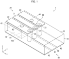
- Fig. 1 is a perspective view illustrating the transmission line 1.
- Fig. 2 (a) to (c) are respectively a bottom view, a plan view, and a rear view of the transmission line illustrated in Fig. 1 .
- Fig. 3 is a cross-sectional view illustrating the transmission line 1.
- (a) is a cross-sectional view taken along A-A' line in (a) of Fig. 1 and a z axis
- (b) is a cross sectional view taken along B-B' line in (a) of Fig. 1 and the z axis.
- the transmission line 1 can be suitably used as an input/output structure for a filter device typified by, for example, the filter device disclosed in Patent Literature 1 and a filter device disclosed in PCT International Publication No. PCT/JP2021/011615 .
- the filter device is provided on a single substrate together with the transmission line 1.
- the present embodiment assumes that the filter device is mounted on a first main surface of a mounting substrate so that a second main surface of a substrate of the filter device and the first main surface of the mounting substrate closely face each other.
- a conductor pattern for achieving a filtering function is provided on a main surface on a side farther from the mounting substrate among the pair of the main surfaces of the substrate.
- the transmission line 1 supplies a high-frequency wave to the filter device, from a main surface on a side closer to the mounting substrate, among the pair of main surfaces of the substrate.
- the present embodiment employs a 60-GHz center frequency of a transmission band of the filter device.
- the center frequency of the transmission band of the filter device is not limited to 60 GHz and can be determined as appropriate, for example, in a band of not less than 30 GHz and not more than 75 GHz.
- the structure of the transmission line 1 and sizes of the components of the transmission line 1 are optimized so as to reduce loss at the center frequency of the transmission band of the filter device as much as possible.
- the transmission line 1 includes a substrate 10, a coplanar line 20, a two-conductor line 30, and a coplanar line 40.
- Each of the coplanar line 20, the two-conductor line 30, and the coplanar line 40 is provided on the substrate 10.
- the "two-conductor line” refers to a high-frequency-wave transmission line including two conductors with different functions: a conductor constituting a signal line and a conductor constituting a ground.
- the ground of the two-conductor line may be constituted by a single conductor or may be constituted by a plurality of conductors.
- Each of a grounded coplanar line, a coplanar line, and a microstrip line is an example of the two-conductor line.
- the two-conductor line 30 is different from a typical grounded coplanar line, coplanar line, and microstrip line and is a high-frequency-wave transmission line that transmits a high-frequency wave in a thickness direction of the substrate 10. Therefore, the two-conductor line 30 is referred to as "two-conductor line”.
- Fig. 1 selectively illustrates only characteristic components of the transmission line 1.
- the substrate 10 is extended in both an x-axis direction and a y-axis direction in the coordinate system illustrated in Fig. 1 .
- the coplanar line 20 is not limited to the range illustrated in Fig. 1 .
- the end portion of the coplanar line 20 opposite to the end portion connected to the two-conductor line 30 is extended in a negative x-axis direction.
- the coplanar line 40 is not limited to the range illustrated in Fig. 1 .
- the end portion of the coplanar line 40 opposite to the end portion connected to the two-conductor line 30 is extended in a positive x-axis direction. Note that in an area lying outside the range illustrated in Fig. 1 and on a negative x-axis direction side, the coplanar line 20 (grounded coplanar line) may be connected with a coplanar line.
- the length along the x-axis direction of a recess 13 described later may be shorter than each of the lengths in the x-axis direction of the signal line pattern 21 and the coplanar patterns 22 and 23 described later.
- a filter device may be provided, as described above.
- the substrate 10 is a board member made of a dielectric.
- the dielectric constituting the substrate 10 is quartz glass.
- the dielectric constituting the substrate 10 is not limited to the quartz glass and can be selected as appropriate.
- Examples of a dielectric other than glass typified by the quartz glass include semiconductors with high resistances and resins.
- the semiconductors with high resistances may be a compound semiconductor typified by gallium arsenide (GaAs) or may be silicon.
- the resins include a fluororesin.
- the dielectric constituting the substrate 10 may be a fluorine compound.
- the substrate 10 has a thickness of 400 pm. Note, however, that the thickness of the substrate 10 is not limited to 400 pm and can be determined as appropriate.
- the main surface 11 is an upper main surface in the state illustrated in Fig. 1 and the main surface 12 is a lower main surface in the state illustrated in Fig. 1 .
- a positive z-axis direction is a direction normal to the main surfaces 11 and 12 from the main surface 12 toward the main surface 11;
- a positive x-axis direction is a direction in which a signal line pattern 21 of the coplanar line 20 described later is extended toward a two-conductor line 30 described later;
- a positive y-axis direction is a direction constituting a right-handed orthogonal coordinate system together with the positive x-axis direction and the positive z-axis direction.
- the main surface 12 of the substrate 10 is provided with a recess 13 formed in an area of the main surface 12 which area overlaps at least part of the signal line pattern 21 described later.
- the recess 13 is configured to overlap part of each coplanar patterns 22 and 23 as well as part of the signal line pattern 21 (see (a) and (b) of Fig. 2 ).
- the recess 13 is constituted by a bottom surface 131 parallel to the main surfaces 11 and 12; and side surfaces perpendicular to the bottom surface 131.
- side surface 132 the side surface close to the two-conductor line 30 described later is referred to as "side surface 132".
- the coplanar line 20 is a two-conductor line provided on the substrate 10, as illustrated in Fig. 1 , (a) of Fig. 2, and (a) of Fig. 3 .
- the coplanar line 20 includes the signal line pattern 21 and the coplanar patterns 22 and 23.
- the signal line pattern 21 and the coplanar patterns 22 and 23 are provided on the main surface 11 of the substrate 10.
- the signal line pattern 21 is an example of a first signal line pattern.
- the coplanar patterns 22 and 23 are an example of a first coplanar pattern.
- the signal line pattern 21 functions as a signal line of the coplanar line 20.
- the coplanar patterns 22 and 23 are provided such that the signal line pattern 21 is held thereby (sandwiched therebetween).
- a ground conductor pattern 42 is a conductor pattern provided so as to cover part of the main surface 12 and the surface of the recess 13 (the bottom surface 131 and the side surfaces) (see (b) of Fig. 2 and (a) of Fig. 3 ).
- the signal line pattern 21 together with the substrate 10 and the coplanar patterns 22 and 23 constitutes a coplanar line. Further, in an area that overlaps the recess 13 when the main surface 12 is seen in plan view from the negative z-axis direction side, a grounded coplanar line is constituted by the signal line pattern 21 together with the substrate 10, the coplanar patterns 22 and 23, and a part of the ground conductor pattern 42 which part is provided on the bottom surface 131 of the recess 13.
- the expression "see in plan view” means either seeing the main surface 11 in plan view from a positive z-axis direction side or seeing the main surface 12 in plan view from a negative z-axis direction side.
- the signal line pattern 21 and the coplanar patterns 22 and 23 are each a thin film made of a conductor.
- the present embodiment employs copper as a conductor constituting each of the signal line pattern 21 and the coplanar patterns 22 and 23.
- ground conductor pattern 42 and the signal line pattern 41 described later are each a thin film made of a conductor.
- the present embodiment employs copper as a conductor constituting each of the signal line pattern 41 and the ground conductor pattern 42.
- the conductor constituting each of the signal line pattern 21, the coplanar patterns 22 and 23, the signal line pattern 41, and the ground conductor pattern 42 is not limited to the copper and can be selected as appropriate.
- the signal line pattern 21 and the coplanar patterns 22 and 23 are each obtained by forming a conductor film (in the present embodiment, a film made of copper) that covers the main surface 11 and subjecting the conductor film to patterning into a desired shape.
- the signal line pattern 41 and the ground conductor pattern 42 are each obtained by, after the recess 13 has been formed in the main surface 12, forming a conductor film (in the present embodiment, a film made of copper) that covers the main surface 12 and the surface of the recess 13 and subjecting the conductor film to patterning into a desired shape. Note that between the signal line pattern 41 and the ground conductor pattern 42, an area from which the conductor film is removed is provided. Therefore, the signal line pattern 41 and the ground conductor pattern 42 are insulated from each other.
- the coplanar pattern 22 and a part of the ground conductor pattern 42 which part is provided on the bottom surface 131 of the recess 13 are short-circuited by a through via 43
- the coplanar pattern 23 and the part of the ground conductor pattern 42 which part is provided on the bottom surface 131 of the recess 13 are short-circuited by a through via 44.
- the through vias 43 and 44 are an example of a pair of third through vias.
- the through vias 43 and 44 are each obtained by forming a conductor film (in the present embodiment, a film made of copper) on an inner wall of a through hole passing through the substrate 10 from the main surface 11 to the bottom surface 131. Therefore, the through vias 43 and 44 are cylindrical members each made of a conductor.
- the through vias 43 and 44 can be each obtained also by filling the through hole with a conductor.
- the through vias 43 and 44 are columnar members each made of a conductor.
- the bottom surface 131 is substantially flat (is flat in the present embodiment), as illustrated in (c) of Fig. 2 and (a) and (b) of Fig. 3 .
- the through vias 43 and 44 are provided in an area in which the recess 13 is provided. More specifically the through vias 43 and 44 are provided, when the main surface 12 is seen in plan view, in areas that are included in the respective coplanar patterns 22 and 23 and that are close to the signal line pattern 21 (in other words, areas on a signal line pattern 21 side). Therefore, the through vias 43 and 44 short-circuit the coplanar patterns 22 and 23 and the part of the ground conductor pattern 42 which part is provided on the bottom surface 131 of the recess 13. Further, the through vias 43 and 44 are provided such that the signal line pattern 21 is held thereby.
- the two-conductor line 30 includes a through via 31 and through vias 32 and 33.
- the through via 31 is an example of a first through via.
- the through vias 32 and 33 are an example of a ground conductor and are also an example of one or more second through vias.
- the through via 31 and the through vias 32 and 33 are each obtained by forming a conductor film (in the present embodiment, a film made of copper) on an inner wall of a through hole passing through the substrate 10 from the main surface 11 to the main surface 12. Therefore, the through via 31 and the through vias 32 and 33 are cylindrical members each made of a conductor.
- a conductor film in the present embodiment, a film made of copper
- the through via 31 and the through vias 32 and 33 can be each obtained also by filling the through hole with a conductor.
- the through via 31 and the through vias 32 and 33 are columnar members each made of a conductor.
- the two through vias 32 and 33 are used as an example of one or more second through vias.
- one of the through vias 32 and 33 may be omitted, or alternatively, the second through vias can be three or more through vias.
- the second through vias in order to increase a symmetric property of a distribution of a capacitance that occurs between the through via 31 and the second through vias, it is preferable that the second through vias be disposed so as to have a symmetric property as great as possible.
- the coplanar line 40 is provided on the main surface 12, as illustrated in (b) of Fig. 2 .
- the coplanar line 40 includes the signal line pattern 41 and a second coplanar pattern constituted by part of the ground conductor pattern 42.
- the signal line pattern 41 is an example of a second signal line pattern.
- the vicinity of an end portion 411, which is one end of the signal line pattern 41 is electrically connected with the through via 31.
- the signal line pattern 41 is substantially parallel (in the present embodiment, is parallel) to the signal line pattern 21 and is extended in a direction away from the signal line pattern 21 (in the positive x-axis direction in (a) and (b) of Fig. 2 ).
- the ground conductor pattern 42 is provided so as to surround the long sides of the signal line pattern 41 (the sides along the x-axis direction in the coordinate system illustrated in Fig. 2 ) and the end portion 411 of the signal line pattern 41 from three directions.
- the ground conductor pattern 42 is a conductor pattern provided so as to cover part of the main surface 12 and the surface of the recess 13 (the bottom surface 131 and the side surfaces) (see (b) of Fig. 2 and (a) of Fig. 3 ).
- the ground conductor pattern 42 has a pattern that surrounds the signal line pattern 41 from the three directions as well as causes the signal line pattern 41 to be held thereby. Part of the ground conductor pattern 42 configured in such a way is an example of the second coplanar pattern.
- the transmission line 1 is configured such that an interval D6 between the signal line pattern 41 and the ground conductor pattern 42 becomes widest at the end portion 411. That is, the interval D6 at the long sides of the signal line pattern 41 is smaller than the interval D6 at the end portion 411. Note that (b) of Fig. 2 illustrates the interval D6 at the end portion 411.
- a configuration is employed in which in the transmission line 1, a distance D1 which is the shortest distance between the through via 31 and the through via 32 is shorter than a distance D2 which is the shortest distance between the through via 31 and the recess 13, as illustrated in (a) of Fig. 2 .
- the distance D2 is an interval between the through via 31 and the side surface 132 of the recess 13 when the main surface 12 is seen in plan view from the negative z-axis direction side.
- the transmission line 1 is configured to be in reflection symmetry with a plane along A-A' line in (a) of Fig. 2 and the z axis as a symmetry plane. Therefore, in the transmission line 1, the shortest distance between the through via 31 and the through via 33 is equal to the distance D1 and is shorter than the distance D2.
- a configuration is employed in which in the transmission line 1, a distance D4 which is the shortest distance between the through vias 32 and 33 is different from a distance D5 which is the shortest distance between the through vias 43 and 44, as illustrated in (b) of Fig. 2 .
- the distance D4 is slightly wider than the distance D5.
- the distance D2 which is the shortest distance between the through via 31 and the recess 13 is equal to a distance D3 which is the shortest distance between each through vias 32 and 33 and the recess 13, as illustrated in (a) of Fig. 2 .
- the distance D2 and the distance D3 may differ from each other. Moving the center of the through via 32 along the C-C' line in (a) of Fig. 2 which is parallel to the x-axis direction makes it possible to change the distance D 1.
- the distance D1 is one of design parameters to match the impedance of the coplanar line 20 and the impedance of the two-conductor line 30.
- the distance D1 As a design parameter, the distance D2 and the distance D3 differ from each other in many cases.
- moving the center of the through via 33 along D-D' line in (a) of Fig. 2 makes it possible to change the shortest distance between the through via 31 and the through via 33.
- a transmission line 1A which is a first variation of the transmission line 1.
- (a) is a rear view of the transmission line 1A and (b) is a bottom view of the transmission line 1A.
- a member having a function identical to that of a member discussed in the section concerning the transmission line 1 is given an identical reference sign, and a description thereof is omitted.
- the single recess 13 is formed in an area overlapping part of the signal line pattern 21 and part of each coplanar patterns 22 and 23.
- a recess group 13A constituted by three recesses 131A, 132A, and 133A is provided in an area of the main surface 12 which area overlaps at least the signal line pattern 21, as illustrated in (a) and (b) of Fig. 4 .
- the recesses 131A, 132A, and 133A are provided in areas overlapping a part of the signal line pattern 21, a part of the coplanar pattern 22, and a part of the coplanar pattern 23, respectively.
- a conductor film formed on the main surface 12 and the surface of the recess group 13A is referred to as a "ground conductor pattern 42A".
- conductor films formed on the surfaces of the recesses 131A, 132A, and 133A constituting the recess group 13A are referred to as ground conductor patterns 421, 422, and 423, respectively.
- the recess provided in an area overlapping at least the signal line pattern 21 may be the single recess 13 or may be the recess group 13A constituted by the three recesses divided.
- the number of the recesses constituting the recess group 13A is not limited to three and can be set as appropriate.
- the recess group 13A can be formed by using a laser processing machine to irradiate quartz glass with laser light to modify (laser-modify) the quartz glass and etching the modified parts of the quartz glass through wet etching.
- the widths and the number of the recesses may be determined depending on a scanning path of the laser light used for the laser processing and the etching time during the wet etching.
- each recess 131A, 132A, and 133A which is on a two-conductor line 30 side is configured to have a semicircular shape when the main surface 12 is seen in plan view. This is because the recess group 13A is formed through the laser modification and the wet etching.
- a configuration is employed in which in the side surface of each recess 131A, 132A, and 133A which is close to the through via 31 and the through vias 32 and 33 in the transmission line 1A, a part close to the through via 31 (specifically, the side surface at the end portion of the recess 131A) recedes further than (is closer to the negative x-axis direction side than) a part close to each of the through vias 32 and 33 (specifically, the side surface at each of the end portions of the recesses 132A and 133A).
- the two-conductor line 30 is constituted by providing, on both sides of the through via 31, the through vias 32 and 33 by which the through via 31 is held.
- the recesses 132A and 133A among the recesses constituting the recess group 13A, can be extended in the positive x-axis direction, thereby allowing the through via 31 and the ground conductor pattern 42A that is provided on the side walls of the extended recesses 132A and 133A to constitute the two-conductor line. Note that this configuration can be applied to a transmission line 1B described later.
- a transmission line 1B which is a second variation of the transmission line 1 and is also one variation of the transmission line 1A.
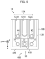
- Fig. 5 is a bottom view of the transmission line 1B.
- the transmission line 1B is based on the transmission line 1A illustrated in Fig. 4 .
- a member having a function identical to that of a member discussed in the sections concerning the transmission line 1 and the transmission line 1A is given an identical reference sign, and a description thereof is omitted.
- the transmission line 1B employs an input/output terminal 40B instead of the coplanar line 40.
- the input/output terminal 40B will be described. Note that, as in the case of the substrate 10 included in the transmission line 1, a substrate 10B included in the transmission line 1B is a board member made of quartz glass. In the present variation, the main surface corresponding to the main surface 12 of the substrate 10 is referred to as "main surface 12B".
- a conductor patch 41B that functions as a signal terminal is provided, when the main surface 12B is seen in plan view, in an area of the main surface 12 which area includes the through via 31 (see Fig. 5 ).
- the conductor patch 41B is spaced from the ground conductor pattern 42.
- the conductor patch 41B is obtained by configuring the signal line pattern 41 illustrated in (c) of Fig. 2 or (b) of Fig. 4 to be short.
- a transmission line 1C which is a third variation of the transmission line 1.
- Fig. 6 is a bottom view of the transmission line 1C.
- the transmission line 1C is based on the transmission line 1 illustrated in Figs. 1 to 3 .
- a member having a function identical to that of a member discussed in the foregoing embodiments is given an identical reference sign, and a description thereof is omitted.
- the through vias 32 and 33 are omitted, and the distance D2 between the through via 31 and the side surface 132 of the recess 13 is decreased.
- the two-conductor line 30 includes the through via 31 and the through vias 32 and 33.
- a two-conductor line 30C includes the through via 31 and a conductor film which is a part of the conductor film constituting the ground conductor pattern 42 and which is provided on the side surface 132 of the recess 13.
- the conductor film provided on the side surface 132 of the recess 13 is an example of a second ground conductor.
- the transmission line 1C includes a substrate 10C, the coplanar line 20, the two-conductor line 30C, and the coplanar line 40.
- the substrate 10C included in the transmission line 1C is a board member made of quartz glass.
- the main surface corresponding to the main surface 12 of the substrate 10 is referred to as "main surface 12C".
- the coplanar line 20 is provided on the substrate 10C.
- the coplanar line 20 includes (i) the signal line pattern 21 provided on the main surface (the main surface corresponding to the main surface 11 of the transmission line 1) opposite to the main surface 12C and (ii) the coplanar patterns 22 and 23 (one example of the first coplanar pattern) by which the signal line pattern 21 is held.
- the coplanar patterns 22 and 23 are each configured to have a length equal to that of the signal line pattern 21. That is, as in the case of the signal line pattern 21, the tips of the coplanar patterns 22 and 23 are located ahead of the through via 31. Note, however, that in the transmission line 1C, the coplanar patterns 22 and 23 may each have a length shorter than that of the signal line pattern 21. In this case, the tips of the coplanar patterns 22 and 23 are preferably closer to a through via 31 side than the side surface 132 of the recess 13 is.
- the two-conductor line 30C is provided to the substrate 10C.
- the two-conductor line 30C includes the through via 31 that is electrically connected with the signal line pattern 21 and that passes through the substrate 10C from the main surface opposite to the main surface 12C to the main surface 12C; and a second ground conductor.
- the recess 13 is provided, when the main surface 12C is seen in plan view, in an area of the main surface 12C which area overlaps at least the signal line pattern 21.
- the recess 13 is provided also, when the main surface 12C is seen in plan view, in an area that overlaps the coplanar patterns 22 and 23.
- the signal line pattern 21, the coplanar patterns 22 and 23, and a part of the ground conductor pattern 42 which part is provided on the bottom surface 131 of the recess 13 constitute a grounded coplanar line.
- the ground conductor is a part of the ground conductor pattern 42 which part is provided on the side surface 132 of the recess 13.
- the present invention is not limited to the embodiments, but can be altered by a skilled person in the art within the scope of the claims.
- the present invention also encompasses, in its technical scope, any embodiment derived by combining technical means disclosed in differing embodiments.
- a transmission line in accordance with Aspect 1 of the present invention includes: (i) a substrate made of a dielectric; (ii) a first coplanar line provided on the substrate, the first coplanar line including: a first signal line pattern which is provided on a first main surface of the substrate; and a first coplanar pattern by which the first signal line pattern is held; and (iii) a two-conductor line provided on the substrate, the two-conductor line including: a first through via that is electrically connected with the first signal line pattern and that passes through the substrate from the first main surface to a second main surface of the substrate; and a ground conductor.
- a configuration is employed in which, in addition to the configuration of the transmission line in accordance with Aspect 1, a recess is provided in an area of the second main surface of the substrate which area overlaps at least the first signal line pattern, said transmission line further comprising a ground conductor pattern that is provided on the second main surface of the substrate and on a surface of the recess and that faces the first signal line pattern, wherein the first coplanar line and the ground conductor pattern that is provided on the surface of the recess constitute a grounded coplanar line, the ground conductor is one or more second through vias passing through the substrate from the first main surface to the second main surface, the one or more second through vias short-circuiting the first coplanar pattern and the ground conductor pattern that is provided on the second main surface, and a shortest distance between the first through via and each of the one or more second through vias is shorter than a shortest distance between the first through via and the recess.
- the two-conductor line when the two-conductor line is designed, it is necessary only to mainly consider a capacitance that occurs between the first through via and the one or more second through vias. This is because the capacitance that may occur between the first through via and the ground conductor pattern formed on the surface of the recess is smaller than the capacitance that occurs between the first through via and the one or more second through vias. Therefore, it is possible to easily design the transmission line.
- a configuration is employed of, in addition to the configuration of the transmission line in accordance with Aspect 2, further including a pair of third through vias short-circuiting the first coplanar pattern and a part of the ground conductor pattern which part is provided on a bottom surface of the recess, the pair of third through vias being provided such that the first signal line pattern is held thereby.
- the coplanar line in which the first signal line pattern and the first coplanar pattern extend parallel to each other is interposed between a grounded coplanar line in which the first signal line pattern and the first coplanar pattern; and the ground conductor pattern extend parallel to each other and the two-conductor line in which the first through via and the one or more second through vias extend parallel to each other.
- each of the pair of third through vias is provided, when seen in plan view, in an area that is included in the first coplanar pattern and that is close to the first signal line pattern.
- a configuration is employed in which, in addition to the configuration of the transmission line in accordance with Aspect 2, the recess is provided, when seen in plan view, in an area of the second main surface of the substrate which area overlaps the first signal line pattern and the first coplanar pattern; the one or more second through vias are a pair of second through vias which are provided such that the first through via is held thereby; and the shortest distance between the first through via and the recess differs from a shortest distance between each of the pair of second through vias and the recess.
- a configuration is employed in which, in addition to the configuration of the transmission line in accordance with Aspect 2, the recess is provided, when seen in plan view, in an area of the second main surface of the substrate which area overlaps the first signal line pattern and the first coplanar pattern; the one or more second through vias are a pair of second through vias which are provided such that the first through via is held thereby; and a side surface of the recess which side surface is close to the first through via and the pair of second through vias has a part that is close to the first through via and that recedes further than a part of the side surface which part is close to each of the pair of second through vias.
- a configuration is employed in which, in addition to the configuration of the transmission line in accordance with Aspect 2, the recess is provided in the area of the second main surface of the substrate which area overlaps at least the first signal line pattern; the ground conductor pattern is provided on the surface of the recess; and the ground conductor is a part of the ground conductor pattern which part is provided on a side surface of the recess, the side surface being close to the first through via.
- the two-conductor line when the two-conductor line is designed, it is necessary only to mainly consider a capacitance that occurs between the first through via and a part provided on the side surface of the recess which side surface is close to the first through via. Therefore, it is possible to easily design the transmission line.
- a configuration is employed in which, in addition to the configuration of the transmission line in accordance with any one of Aspects 2 to 7, a conductor patch that functions as a signal terminal and that is spaced from the ground conductor pattern is provided, when seen in plan view, in an area of the second main surface of the substrate which area includes the first through via.
- the above configuration eliminates the need for further providing, on the second main surface, a two-conductor line (for example, a coplanar line) for causing the signal line to be electrically connected with the first through via in a case where the transmission line is mounted onto a mounting substrate. Therefore, it is possible to reduce a size of the substrate constituting the transmission line.
- a two-conductor line for example, a coplanar line
- a configuration is employed of, in addition to the configuration of the transmission line in accordance with any one of Aspects 2 to 7, further including a second coplanar line provided on the second main surface, the second coplanar line including: a second signal line pattern which is electrically connected with the first through via; and a second coplanar pattern by which the second signal line pattern is held.
- a configuration is employed in which, in addition to the configuration of the transmission line in accordance with Aspect 9, the second signal line pattern of the second coplanar line is substantially parallel to the first signal line pattern of the first coplanar line and extends in a direction away from the first signal line pattern of the first coplanar line; the second coplanar pattern surrounds the second signal line pattern of the second coplanar line from at least three directions; and an interval between the second signal line pattern of the second coplanar line and the second coplanar pattern of the second coplanar line is widest at an end portion of the second signal line pattern of the second coplanar line which end portion is located on a recess side.
- the above configuration makes it easier to match the impedance of the two-conductor line and the impedance of the second coplanar line and thus makes it possible to further reduce return loss.
Landscapes
- Structure Of Printed Boards (AREA)
Abstract
Description
- The present invention relates to a transmission line.
-
Figs. 1 to 4 ofPatent Literature 1 disclose a filter device in which two microstrip lines electromagnetically coupled to each other are used. This filter device includes a substrate made of a dielectric, a pair of signal lines provided on a first main surface of the substrate (inPatent Literature 1, referred to as "stubs 6a and 6b" and "patches 8a and 8b"), a ground conductor provided on a second main surface of the substrate (inPatent Literature 1, referred to as "ground conductor surface 10"), and a pair of input/output structures (inPatent Literature 1, referred to as "input and output taps 14a and 14b" and "metallized holes"). The stubs 6a and 6b are conductor patterns each having a strip shape. The input and output taps 14a and 14b are conductor patterns provided so as to protrude from midway points of the stubs 6a and 6b, respectively. - In a case where this filter device is mounted on a mounting substrate, the second main surface (the main surface opposite to the main surface on which a signal line is provided) of the substrate of the filter device is typically caused to face a first main surface of the mounting substrate. Therefore, a through via (in
Patent Literature 1, referred to as "metallized hole") passing through the pair of main surfaces of the substrate is provided in the vicinity of each of end portions opposite to those which are connected to the stubs 6a and 6b, among the end portions of the input and output taps 14a and 14b. The through via being connected to each of the input and output taps 14a and 14b enables supply of a high-frequency wave from the second main surface side of the substrate of the filter device to the filter device. - [Patent Literature 1]
Specification ofUS Patent No. 5343176 - However, in such an input/output structure, when the high-frequency wave to be transmitted has a higher frequency, it is more likely to increase return loss. This is because in the input/output structure, the one through via, which is not enough to serve as a transmission line, serves to transmit a high-frequency wave between the pair of main surfaces of the substrate.
- An aspect of the present invention has been achieved in light of the foregoing problem. It is an object of the aspect of the present invention to, in a transmission line that transmits a high-frequency wave between a pair of main surfaces of a substrate, reduce return loss, as compared with the input/output structure included in the filter device disclosed in
Patent Literature 1. - In order to solve the foregoing problem, a transmission line in accordance with
Aspect 1 of the present invention includes: (i) a substrate made of a dielectric; (ii) a first coplanar line provided on the substrate, the first coplanar line including: a first signal line pattern which is provided on a first main surface of the substrate; and a first coplanar pattern by which the first signal line pattern is held; and (iii) a two-conductor line provided on the substrate, the two-conductor line including: a first through via that is electrically connected with the first signal line pattern and that passes through the substrate from the first main surface to a second main surface of the substrate; and a ground conductor. - According to an aspect of the present invention, it is possible to, in a transmission line that transmits a high-frequency wave between a pair of main surfaces of a substrate, reduce return loss, as compared with the input/output structure included in the filter device disclosed in
Patent Literature 1. -
-
Fig. 1 is a perspective view illustrating a transmission line in accordance with an embodiment of the present invention. - (a) to (c) of
Fig. 2 are respectively a bottom view, a plan view, and a rear view of the transmission line illustrated inFig. 1 . -
Fig. 3 is a cross-sectional view illustrating the transmission line illustrated inFig. 1 . (a) is a cross-sectional view taken along A-A' line in (a) ofFig. 1 and a z axis, and (b) is a cross-sectional view taken along B-B' line in (a) ofFig. 1 and the z axis. - (a) of
Fig. 4 is a rear view illustrating a first variation of the transmission line illustrated inFig. 1 , and (b) ofFig. 4 is a bottom view illustrating the first variation. -
Fig. 5 is a bottom view of a second variation of the transmission line illustrated inFig. 1 . -
Fig. 6 is a bottom view of a third variation of the transmission line illustrated inFig. 1 . - With reference to
Figs. 1 to Fig. 3 , the following description will discuss atransmission line 1 in accordance with an embodiment of the present invention.Fig. 1 is a perspective view illustrating thetransmission line 1. InFig. 2, (a) to (c) are respectively a bottom view, a plan view, and a rear view of the transmission line illustrated inFig. 1 .Fig. 3 is a cross-sectional view illustrating thetransmission line 1. InFig. 3, (a) is a cross-sectional view taken along A-A' line in (a) ofFig. 1 and a z axis, and (b) is a cross sectional view taken along B-B' line in (a) ofFig. 1 and the z axis. - The
transmission line 1 can be suitably used as an input/output structure for a filter device typified by, for example, the filter device disclosed inPatent Literature 1 and a filter device disclosed in PCT International Publication No.PCT/JP2021/011615 transmission line 1 is used as an input/output structure for such a filter device, the filter device is provided on a single substrate together with thetransmission line 1. - The present embodiment assumes that the filter device is mounted on a first main surface of a mounting substrate so that a second main surface of a substrate of the filter device and the first main surface of the mounting substrate closely face each other. In this case, in the filter device, a conductor pattern for achieving a filtering function is provided on a main surface on a side farther from the mounting substrate among the pair of the main surfaces of the substrate. It is assumed that the
transmission line 1 supplies a high-frequency wave to the filter device, from a main surface on a side closer to the mounting substrate, among the pair of main surfaces of the substrate. - Note that the present embodiment employs a 60-GHz center frequency of a transmission band of the filter device. However, the center frequency of the transmission band of the filter device is not limited to 60 GHz and can be determined as appropriate, for example, in a band of not less than 30 GHz and not more than 75 GHz. The structure of the
transmission line 1 and sizes of the components of thetransmission line 1 are optimized so as to reduce loss at the center frequency of the transmission band of the filter device as much as possible. - As illustrated in
Fig. 1 , thetransmission line 1 includes asubstrate 10, acoplanar line 20, a two-conductor line 30, and acoplanar line 40. Each of thecoplanar line 20, the two-conductor line 30, and thecoplanar line 40 is provided on thesubstrate 10. In the present specification, the "two-conductor line" refers to a high-frequency-wave transmission line including two conductors with different functions: a conductor constituting a signal line and a conductor constituting a ground. In the present specification, the ground of the two-conductor line may be constituted by a single conductor or may be constituted by a plurality of conductors. Each of a grounded coplanar line, a coplanar line, and a microstrip line is an example of the two-conductor line. Note that the two-conductor line 30 is different from a typical grounded coplanar line, coplanar line, and microstrip line and is a high-frequency-wave transmission line that transmits a high-frequency wave in a thickness direction of thesubstrate 10. Therefore, the two-conductor line 30 is referred to as "two-conductor line". - In an aspect of the present invention, like a second variation of the
transmission line 1 which will be described later with reference toFig. 5 , it is possible to use aconductor patch 41B instead of asignal line pattern 41 included in thecoplanar line 40 of thetransmission line 1. That is, in an aspect of the present invention, it is possible to omit thecoplanar line 40. Note thatFig. 1 selectively illustrates only characteristic components of thetransmission line 1. Thesubstrate 10 is extended in both an x-axis direction and a y-axis direction in the coordinate system illustrated inFig. 1 . In addition, thecoplanar line 20 is not limited to the range illustrated inFig. 1 . The end portion of thecoplanar line 20 opposite to the end portion connected to the two-conductor line 30 is extended in a negative x-axis direction. Further, thecoplanar line 40 is not limited to the range illustrated inFig. 1 . The end portion of thecoplanar line 40 opposite to the end portion connected to the two-conductor line 30 is extended in a positive x-axis direction. Note that in an area lying outside the range illustrated inFig. 1 and on a negative x-axis direction side, the coplanar line 20 (grounded coplanar line) may be connected with a coplanar line. That is, the length along the x-axis direction of arecess 13 described later may be shorter than each of the lengths in the x-axis direction of thesignal line pattern 21 and thecoplanar patterns substrate 10, a filter device may be provided, as described above. - The
substrate 10 is a board member made of a dielectric. In the present embodiment, the dielectric constituting thesubstrate 10 is quartz glass. However, the dielectric constituting thesubstrate 10 is not limited to the quartz glass and can be selected as appropriate. Examples of a dielectric other than glass typified by the quartz glass include semiconductors with high resistances and resins. The semiconductors with high resistances may be a compound semiconductor typified by gallium arsenide (GaAs) or may be silicon. Examples of the resins include a fluororesin. The dielectric constituting thesubstrate 10 may be a fluorine compound. - In the present embodiment, the
substrate 10 has a thickness of 400 pm. Note, however, that the thickness of thesubstrate 10 is not limited to 400 pm and can be determined as appropriate. - Among a pair of
main surfaces substrate 10, themain surface 11 is an upper main surface in the state illustrated inFig. 1 and themain surface 12 is a lower main surface in the state illustrated inFig. 1 . - In the coordinate system illustrated in
Fig. 1 , a positive z-axis direction is a direction normal to themain surfaces main surface 12 toward themain surface 11; a positive x-axis direction is a direction in which asignal line pattern 21 of thecoplanar line 20 described later is extended toward a two-conductor line 30 described later; and a positive y-axis direction is a direction constituting a right-handed orthogonal coordinate system together with the positive x-axis direction and the positive z-axis direction. - The
main surface 12 of thesubstrate 10 is provided with arecess 13 formed in an area of themain surface 12 which area overlaps at least part of thesignal line pattern 21 described later. In the present embodiment, therecess 13 is configured to overlap part of eachcoplanar patterns Fig. 2 ). - The
recess 13 is constituted by abottom surface 131 parallel to themain surfaces bottom surface 131. Hereinafter, among the side surfaces, the side surface close to the two-conductor line 30 described later is referred to as "side surface 132". - The
coplanar line 20 is a two-conductor line provided on thesubstrate 10, as illustrated inFig. 1 , (a) ofFig. 2, and (a) ofFig. 3 . Thecoplanar line 20 includes thesignal line pattern 21 and thecoplanar patterns - The
signal line pattern 21 and thecoplanar patterns main surface 11 of thesubstrate 10. Thesignal line pattern 21 is an example of a first signal line pattern. Thecoplanar patterns - The
signal line pattern 21 functions as a signal line of thecoplanar line 20. - The
coplanar patterns signal line pattern 21 is held thereby (sandwiched therebetween). - A
ground conductor pattern 42 is a conductor pattern provided so as to cover part of themain surface 12 and the surface of the recess 13 (thebottom surface 131 and the side surfaces) (see (b) ofFig. 2 and (a) ofFig. 3 ). - The
signal line pattern 21 together with thesubstrate 10 and thecoplanar patterns recess 13 when themain surface 12 is seen in plan view from the negative z-axis direction side, a grounded coplanar line is constituted by thesignal line pattern 21 together with thesubstrate 10, thecoplanar patterns ground conductor pattern 42 which part is provided on thebottom surface 131 of therecess 13. Note that hereinafter, the expression "see in plan view" means either seeing themain surface 11 in plan view from a positive z-axis direction side or seeing themain surface 12 in plan view from a negative z-axis direction side. - The
signal line pattern 21 and thecoplanar patterns signal line pattern 21 and thecoplanar patterns - Similarly, the
ground conductor pattern 42 and thesignal line pattern 41 described later are each a thin film made of a conductor. The present embodiment employs copper as a conductor constituting each of thesignal line pattern 41 and theground conductor pattern 42. - However, the conductor constituting each of the
signal line pattern 21, thecoplanar patterns signal line pattern 41, and theground conductor pattern 42 is not limited to the copper and can be selected as appropriate. - The
signal line pattern 21 and thecoplanar patterns main surface 11 and subjecting the conductor film to patterning into a desired shape. Thesignal line pattern 41 and theground conductor pattern 42 are each obtained by, after therecess 13 has been formed in themain surface 12, forming a conductor film (in the present embodiment, a film made of copper) that covers themain surface 12 and the surface of therecess 13 and subjecting the conductor film to patterning into a desired shape. Note that between thesignal line pattern 41 and theground conductor pattern 42, an area from which the conductor film is removed is provided. Therefore, thesignal line pattern 41 and theground conductor pattern 42 are insulated from each other. - In the
coplanar line 20, thecoplanar pattern 22 and a part of theground conductor pattern 42 which part is provided on thebottom surface 131 of therecess 13 are short-circuited by a through via 43, and thecoplanar pattern 23 and the part of theground conductor pattern 42 which part is provided on thebottom surface 131 of therecess 13 are short-circuited by a through via 44. The throughvias - The through
vias substrate 10 from themain surface 11 to thebottom surface 131. Therefore, the throughvias - Note, however, that the through
vias vias - The
bottom surface 131 is substantially flat (is flat in the present embodiment), as illustrated in (c) ofFig. 2 and (a) and (b) ofFig. 3 . - As illustrated in (b) of
Fig. 2 , when themain surface 12 is seen in plan view, areas in which the throughvias recess 13 is provided. More specifically the throughvias main surface 12 is seen in plan view, in areas that are included in the respectivecoplanar patterns signal line pattern 21 side). Therefore, the throughvias coplanar patterns ground conductor pattern 42 which part is provided on thebottom surface 131 of therecess 13. Further, the throughvias signal line pattern 21 is held thereby. - As illustrated in
Fig. 1 , the two-conductor line 30 includes a through via 31 and throughvias vias - The through via 31 and the through
vias substrate 10 from themain surface 11 to themain surface 12. Therefore, the through via 31 and the throughvias - Note, however, that the through via 31 and the through
vias vias - In the present embodiment, the two through
vias vias - The
coplanar line 40 is provided on themain surface 12, as illustrated in (b) ofFig. 2 . Thecoplanar line 40 includes thesignal line pattern 41 and a second coplanar pattern constituted by part of theground conductor pattern 42. - The
signal line pattern 41 is an example of a second signal line pattern. In thesignal line pattern 41, the vicinity of anend portion 411, which is one end of thesignal line pattern 41, is electrically connected with the through via 31. Thesignal line pattern 41 is substantially parallel (in the present embodiment, is parallel) to thesignal line pattern 21 and is extended in a direction away from the signal line pattern 21 (in the positive x-axis direction in (a) and (b) ofFig. 2 ). - The
ground conductor pattern 42 is provided so as to surround the long sides of the signal line pattern 41 (the sides along the x-axis direction in the coordinate system illustrated inFig. 2 ) and theend portion 411 of thesignal line pattern 41 from three directions. As described above, theground conductor pattern 42 is a conductor pattern provided so as to cover part of themain surface 12 and the surface of the recess 13 (thebottom surface 131 and the side surfaces) (see (b) ofFig. 2 and (a) ofFig. 3 ). Theground conductor pattern 42 has a pattern that surrounds thesignal line pattern 41 from the three directions as well as causes thesignal line pattern 41 to be held thereby. Part of theground conductor pattern 42 configured in such a way is an example of the second coplanar pattern. - The
transmission line 1 is configured such that an interval D6 between thesignal line pattern 41 and theground conductor pattern 42 becomes widest at theend portion 411. That is, the interval D6 at the long sides of thesignal line pattern 41 is smaller than the interval D6 at theend portion 411. Note that (b) ofFig. 2 illustrates the interval D6 at theend portion 411. - Note that the same description in the section concerning the
coplanar line 20 applies to a conductor film constituting thesignal line pattern 41 and a conductor film constituting theground conductor pattern 42, and thus the descriptions thereof are omitted here. - A configuration is employed in which in the
transmission line 1, a distance D1 which is the shortest distance between the through via 31 and the through via 32 is shorter than a distance D2 which is the shortest distance between the through via 31 and therecess 13, as illustrated in (a) ofFig. 2 . The distance D2 is an interval between the through via 31 and theside surface 132 of therecess 13 when themain surface 12 is seen in plan view from the negative z-axis direction side. Note that thetransmission line 1 is configured to be in reflection symmetry with a plane along A-A' line in (a) ofFig. 2 and the z axis as a symmetry plane. Therefore, in thetransmission line 1, the shortest distance between the through via 31 and the through via 33 is equal to the distance D1 and is shorter than the distance D2. - Further, a configuration is employed in which in the
transmission line 1, a distance D4 which is the shortest distance between the throughvias vias Fig. 2 . In thetransmission line 1 illustrated in (b) ofFig. 2 , the distance D4 is slightly wider than the distance D5. - Furthermore, a configuration is employed in which in the
transmission line 1, when themain surface 11 is seen in plan view, the distance D2 which is the shortest distance between the through via 31 and therecess 13 is equal to a distance D3 which is the shortest distance between each throughvias recess 13, as illustrated in (a) ofFig. 2 . Note, however, that the distance D2 and the distance D3 may differ from each other. Moving the center of the through via 32 along the C-C' line in (a) ofFig. 2 which is parallel to the x-axis direction makes it possible to change thedistance D 1. The distance D1 is one of design parameters to match the impedance of thecoplanar line 20 and the impedance of the two-conductor line 30. When the impedance of thecoplanar line 20 and the impedance of the two-conductor line 30 are matched using the distance D1 as a design parameter, the distance D2 and the distance D3 differ from each other in many cases. Similarly, moving the center of the through via 33 along D-D' line in (a) ofFig. 2 makes it possible to change the shortest distance between the through via 31 and the through via 33. - With reference to
Fig. 4 , the following description will discuss atransmission line 1A which is a first variation of thetransmission line 1. InFig. 4, (a) is a rear view of thetransmission line 1A and (b) is a bottom view of thetransmission line 1A. For convenience of description, a member having a function identical to that of a member discussed in the section concerning thetransmission line 1 is given an identical reference sign, and a description thereof is omitted. - In the
transmission line 1 illustrated in (b) and (c) ofFig. 2 , thesingle recess 13 is formed in an area overlapping part of thesignal line pattern 21 and part of eachcoplanar patterns - On the other hand, in the
transmission line 1A, arecess group 13A constituted by threerecesses main surface 12 which area overlaps at least thesignal line pattern 21, as illustrated in (a) and (b) ofFig. 4 . Therecesses signal line pattern 21, a part of thecoplanar pattern 22, and a part of thecoplanar pattern 23, respectively. Note that in the present variation, a conductor film formed on themain surface 12 and the surface of therecess group 13A is referred to as a "ground conductor pattern 42A". Further, conductor films formed on the surfaces of therecesses recess group 13A are referred to asground conductor patterns - As such, in an aspect of the present invention, the recess provided in an area overlapping at least the
signal line pattern 21 may be thesingle recess 13 or may be therecess group 13A constituted by the three recesses divided. Further, the number of the recesses constituting therecess group 13A is not limited to three and can be set as appropriate. For example, therecess group 13A can be formed by using a laser processing machine to irradiate quartz glass with laser light to modify (laser-modify) the quartz glass and etching the modified parts of the quartz glass through wet etching. In this case, the widths and the number of the recesses may be determined depending on a scanning path of the laser light used for the laser processing and the etching time during the wet etching. - In addition, in the
transmission line 1A, an end portion of eachrecess conductor line 30 side is configured to have a semicircular shape when themain surface 12 is seen in plan view. This is because therecess group 13A is formed through the laser modification and the wet etching. - In addition, a configuration is employed in which in the side surface of each
recess vias transmission line 1A, a part close to the through via 31 (specifically, the side surface at the end portion of therecess 131A) recedes further than (is closer to the negative x-axis direction side than) a part close to each of the throughvias 32 and 33 (specifically, the side surface at each of the end portions of therecesses - Note that in the
transmission line 1A, as in the case of thetransmission line 1, the two-conductor line 30 is constituted by providing, on both sides of the through via 31, the throughvias vias recesses recess group 13A, can be extended in the positive x-axis direction, thereby allowing the through via 31 and theground conductor pattern 42A that is provided on the side walls of theextended recesses transmission line 1B described later. - With reference to
Fig. 5 , the following description will discuss atransmission line 1B which is a second variation of thetransmission line 1 and is also one variation of thetransmission line 1A.Fig. 5 is a bottom view of thetransmission line 1B. Thetransmission line 1B is based on thetransmission line 1A illustrated inFig. 4 . For convenience of description, a member having a function identical to that of a member discussed in the sections concerning thetransmission line 1 and thetransmission line 1A is given an identical reference sign, and a description thereof is omitted. - In comparison with the
transmission line 1 and thetransmission line 1A, thetransmission line 1B employs an input/output terminal 40B instead of thecoplanar line 40. In the present variation, the input/output terminal 40B will be described. Note that, as in the case of thesubstrate 10 included in thetransmission line 1, asubstrate 10B included in thetransmission line 1B is a board member made of quartz glass. In the present variation, the main surface corresponding to themain surface 12 of thesubstrate 10 is referred to as "main surface 12B". - In the
transmission line 1B, aconductor patch 41B that functions as a signal terminal is provided, when themain surface 12B is seen in plan view, in an area of themain surface 12 which area includes the through via 31 (seeFig. 5 ). Theconductor patch 41B is spaced from theground conductor pattern 42. Theconductor patch 41B is obtained by configuring thesignal line pattern 41 illustrated in (c) ofFig. 2 or (b) ofFig. 4 to be short. - Even in a case where, as described above, the
conductor patch 41B is provided only in the area which includes the through via 31, use of a technique called "pad on via" enables connection of the input/output terminal 40B to an input/output terminal provided on a first main surface of the mounting substrate. - With reference to
Fig. 6 , the following description will discuss a transmission line 1C which is a third variation of thetransmission line 1.Fig. 6 is a bottom view of the transmission line 1C. The transmission line 1C is based on thetransmission line 1 illustrated inFigs. 1 to 3 . For convenience of description, a member having a function identical to that of a member discussed in the foregoing embodiments is given an identical reference sign, and a description thereof is omitted. - In comparison with the
transmission line 1, in the transmission line 1C, the throughvias side surface 132 of therecess 13 is decreased. In thetransmission line 1, the two-conductor line 30 includes the through via 31 and the throughvias conductor line 30C includes the through via 31 and a conductor film which is a part of the conductor film constituting theground conductor pattern 42 and which is provided on theside surface 132 of therecess 13. The conductor film provided on theside surface 132 of therecess 13 is an example of a second ground conductor. - As such, the transmission line 1C includes a
substrate 10C, thecoplanar line 20, the two-conductor line 30C, and thecoplanar line 40. Note that, as in the case of thesubstrate 10 included in thetransmission line 1, thesubstrate 10C included in the transmission line 1C is a board member made of quartz glass. In the present variation, the main surface corresponding to themain surface 12 of thesubstrate 10 is referred to as "main surface 12C". - The
coplanar line 20 is provided on thesubstrate 10C. Thecoplanar line 20 includes (i) thesignal line pattern 21 provided on the main surface (the main surface corresponding to themain surface 11 of the transmission line 1) opposite to themain surface 12C and (ii) thecoplanar patterns 22 and 23 (one example of the first coplanar pattern) by which thesignal line pattern 21 is held. - In the transmission line 1C, the
coplanar patterns signal line pattern 21. That is, as in the case of thesignal line pattern 21, the tips of thecoplanar patterns coplanar patterns signal line pattern 21. In this case, the tips of thecoplanar patterns side surface 132 of therecess 13 is. - The two-
conductor line 30C is provided to thesubstrate 10C. The two-conductor line 30C includes the through via 31 that is electrically connected with thesignal line pattern 21 and that passes through thesubstrate 10C from the main surface opposite to themain surface 12C to themain surface 12C; and a second ground conductor. - The
recess 13 is provided, when themain surface 12C is seen in plan view, in an area of themain surface 12C which area overlaps at least thesignal line pattern 21. In the present variation, therecess 13 is provided also, when themain surface 12C is seen in plan view, in an area that overlaps thecoplanar patterns - In the transmission line 1C, the
signal line pattern 21, thecoplanar patterns ground conductor pattern 42 which part is provided on thebottom surface 131 of therecess 13 constitute a grounded coplanar line. In the transmission line 1C, the ground conductor is a part of theground conductor pattern 42 which part is provided on theside surface 132 of therecess 13. - The present invention is not limited to the embodiments, but can be altered by a skilled person in the art within the scope of the claims. The present invention also encompasses, in its technical scope, any embodiment derived by combining technical means disclosed in differing embodiments.
- Aspects of the present invention can also be expressed as follows:
A transmission line in accordance withAspect 1 of the present invention includes: (i) a substrate made of a dielectric; (ii) a first coplanar line provided on the substrate, the first coplanar line including: a first signal line pattern which is provided on a first main surface of the substrate; and a first coplanar pattern by which the first signal line pattern is held; and (iii) a two-conductor line provided on the substrate, the two-conductor line including: a first through via that is electrically connected with the first signal line pattern and that passes through the substrate from the first main surface to a second main surface of the substrate; and a ground conductor. - According to the above configuration, it is possible to use the two-conductor line including the first through via and the ground conductor in order to transmit a high-frequency wave between the pair of main surfaces of the substrate. Therefore, it is possible to reduce return loss, as compared with the input/output structure included in the filter device of
Patent Literature 1. - In a transmission line in accordance with Aspect 2 of the present invention, a configuration is employed in which, in addition to the configuration of the transmission line in accordance with
Aspect 1, a recess is provided in an area of the second main surface of the substrate which area overlaps at least the first signal line pattern, said transmission line further comprising a ground conductor pattern that is provided on the second main surface of the substrate and on a surface of the recess and that faces the first signal line pattern, wherein the first coplanar line and the ground conductor pattern that is provided on the surface of the recess constitute a grounded coplanar line, the ground conductor is one or more second through vias passing through the substrate from the first main surface to the second main surface, the one or more second through vias short-circuiting the first coplanar pattern and the ground conductor pattern that is provided on the second main surface, and a shortest distance between the first through via and each of the one or more second through vias is shorter than a shortest distance between the first through via and the recess. - According to the above configuration, when the two-conductor line is designed, it is necessary only to mainly consider a capacitance that occurs between the first through via and the one or more second through vias. This is because the capacitance that may occur between the first through via and the ground conductor pattern formed on the surface of the recess is smaller than the capacitance that occurs between the first through via and the one or more second through vias. Therefore, it is possible to easily design the transmission line.
- In a transmission line in accordance with Aspect 3 of the present invention, a configuration is employed of, in addition to the configuration of the transmission line in accordance with Aspect 2, further including a pair of third through vias short-circuiting the first coplanar pattern and a part of the ground conductor pattern which part is provided on a bottom surface of the recess, the pair of third through vias being provided such that the first signal line pattern is held thereby.
- In a transmission line in accordance with an aspect of the present invention, the coplanar line in which the first signal line pattern and the first coplanar pattern extend parallel to each other is interposed between a grounded coplanar line in which the first signal line pattern and the first coplanar pattern; and the ground conductor pattern extend parallel to each other and the two-conductor line in which the first through via and the one or more second through vias extend parallel to each other. According to the above configuration, it is possible to smoothly switch between the waveguide mode in the grounded coplanar line and the waveguide mode in the coplanar line, since the pair of third through vias can short-circuit the ground conductor pattern and the first coplanar pattern. Therefore, it is possible to further reduce the return loss.
- In a transmission line in accordance with
Aspect 4 of the present invention, a configuration is employed in which, in addition to the configuration of the transmission line in accordance with Aspect 3, each of the pair of third through vias is provided, when seen in plan view, in an area that is included in the first coplanar pattern and that is close to the first signal line pattern. - In a case where a high-frequency wave is transmitted through the first coplanar line, a current distribution caused by the high-frequency wave likely becomes high in an edge portion in which the first signal line pattern and the first coplanar pattern face each other and are close to each other. According to the above configuration, it is possible to short-circuit the first coplanar pattern and the ground conductor pattern in an area which is included in the first coplanar pattern, which is close to the first signal line pattern, and in which the current distribution is high. Thus, it is possible to cause the current distribution of the first coplanar pattern to be close to the current distribution of each of the pair of third through vias. Therefore, it is possible to enhance continuity of the impedance at a boundary between the grounded coplanar line and the first coplanar line.
- In a transmission line in accordance with Aspect 5 of the present invention, a configuration is employed in which, in addition to the configuration of the transmission line in accordance with Aspect 2, the recess is provided, when seen in plan view, in an area of the second main surface of the substrate which area overlaps the first signal line pattern and the first coplanar pattern; the one or more second through vias are a pair of second through vias which are provided such that the first through via is held thereby; and the shortest distance between the first through via and the recess differs from a shortest distance between each of the pair of second through vias and the recess.
- In a case were the impedance of the grounded coplanar line and the impedance of the two-conductor line are matched as exactly as possible, it is possible to adjust the shortest distance between the pair of second through vias like
Aspect 4 or alternatively to adjust the shortest distance between each of the pair of second through vias and the recess like the present aspect. According to the above configuration, as in the case ofAspect 4, it is possible to enhance the impedance matching between the grounded coplanar line and the two-conductor line, resulting in reduction in the return loss. - In a transmission line in accordance with Aspect 6 of the present invention, a configuration is employed in which, in addition to the configuration of the transmission line in accordance with Aspect 2, the recess is provided, when seen in plan view, in an area of the second main surface of the substrate which area overlaps the first signal line pattern and the first coplanar pattern; the one or more second through vias are a pair of second through vias which are provided such that the first through via is held thereby; and a side surface of the recess which side surface is close to the first through via and the pair of second through vias has a part that is close to the first through via and that recedes further than a part of the side surface which part is close to each of the pair of second through vias.
- According to the above configuration, it is possible to decrease the entire length of the transmission line (the length in a direction along the first signal line pattern).
- In a transmission line in accordance with Aspect 7 of the present invention, a configuration is employed in which, in addition to the configuration of the transmission line in accordance with Aspect 2, the recess is provided in the area of the second main surface of the substrate which area overlaps at least the first signal line pattern; the ground conductor pattern is provided on the surface of the recess; and the ground conductor is a part of the ground conductor pattern which part is provided on a side surface of the recess, the side surface being close to the first through via.
- According to the above configuration, when the two-conductor line is designed, it is necessary only to mainly consider a capacitance that occurs between the first through via and a part provided on the side surface of the recess which side surface is close to the first through via. Therefore, it is possible to easily design the transmission line.
- In a transmission line in accordance with Aspect 8 of the present invention, a configuration is employed in which, in addition to the configuration of the transmission line in accordance with any one of Aspects 2 to 7, a conductor patch that functions as a signal terminal and that is spaced from the ground conductor pattern is provided, when seen in plan view, in an area of the second main surface of the substrate which area includes the first through via.
- The above configuration eliminates the need for further providing, on the second main surface, a two-conductor line (for example, a coplanar line) for causing the signal line to be electrically connected with the first through via in a case where the transmission line is mounted onto a mounting substrate. Therefore, it is possible to reduce a size of the substrate constituting the transmission line.
- In a transmission line in accordance with Aspect 9 of the present invention, a configuration is employed of, in addition to the configuration of the transmission line in accordance with any one of Aspects 2 to 7, further including a second coplanar line provided on the second main surface, the second coplanar line including: a second signal line pattern which is electrically connected with the first through via; and a second coplanar pattern by which the second signal line pattern is held.
- According to the above configuration, it is possible to reduce the return loss that may occur in a case where the second signal line pattern electrically connected with the first through via is provided on the second main surface.
- In a transmission line in accordance with
Aspect 10 of the present invention, a configuration is employed in which, in addition to the configuration of the transmission line in accordance with Aspect 9, the second signal line pattern of the second coplanar line is substantially parallel to the first signal line pattern of the first coplanar line and extends in a direction away from the first signal line pattern of the first coplanar line; the second coplanar pattern surrounds the second signal line pattern of the second coplanar line from at least three directions; and an interval between the second signal line pattern of the second coplanar line and the second coplanar pattern of the second coplanar line is widest at an end portion of the second signal line pattern of the second coplanar line which end portion is located on a recess side. - The above configuration makes it easier to match the impedance of the two-conductor line and the impedance of the second coplanar line and thus makes it possible to further reduce return loss.
-
- 1, 1A, 1B, and 1C Transmission line
- 10, 10B, and 10C Substrate
- 11 Main surface (first main surface)
- 12, 12B, and 12C Main surface (second main surface)
- 13 Recess
- 131 Bottom surface
- 132 Side surface
- 13A Recess group
- 131A, 132A, and 133A Recess
- 20 Coplanar line (a part of which constitutes a grounded coplanar line)
- 21 Signal line pattern
- 22 and 23 Coplanar pattern (first coplanar pattern)
- 30 Two-conductor line
- 31 Through via (first through via)
- 32 and 33 Through via (second through via, one example of second ground conductor)
- 40 Coplanar line
- 41 Signal line pattern
- 42 Ground conductor pattern (serving also as second coplanar pattern)
- 43 and 44 Through via (third through via)
Claims (10)
- A transmission line comprising:(i) a substrate made of a dielectric;(ii) a first coplanar line provided on the substrate, the first coplanar line including:a first signal line pattern which is provided on a first main surface of the substrate; anda first coplanar pattern by which the first signal line pattern is held; and(iii) a two-conductor line provided on the substrate, the two-conductor line including:a first through via that is electrically connected with the first signal line pattern and that passes through the substrate from the first main surface to a second main surface of the substrate; anda ground conductor.
- The transmission line according to claim 1, whereina recess is provided in an area of the second main surface of the substrate which area overlaps at least the first signal line pattern,said transmission line further comprising a ground conductor pattern that is provided on the second main surface of the substrate and on a surface of the recess and that faces the first signal line pattern, whereinthe first coplanar line and the ground conductor pattern that is provided on the surface of the recess constitute a grounded coplanar line,the ground conductor is one or more second through vias passing through the substrate from the first main surface to the second main surface, the one or more second through vias short-circuiting the first coplanar pattern and the ground conductor pattern that is provided on the second main surface, anda shortest distance between the first through via and each of the one or more second through vias is shorter than a shortest distance between the first through via and the recess.
- The transmission line according to claim 2, further comprising a pair of third through vias short-circuiting the first coplanar pattern and a part of the ground conductor pattern which part is provided on a bottom surface of the recess, the pair of third through vias being provided such that the first signal line pattern is held thereby.
- The transmission line according to claim 3, wherein each of the pair of third through vias is provided, when seen in plan view, in an area that is included in the first coplanar pattern and that is close to the first signal line pattern.
- The transmission line according to claim 2, wherein:the recess is provided, when seen in plan view, in an area of the second main surface of the substrate which area overlaps the first signal line pattern and the first coplanar pattern;the one or more second through vias are a pair of second through vias which are provided such that the first through via is held thereby; andthe shortest distance between the first through via and the recess differs from a shortest distance between each of the pair of second through vias and the recess.
- The transmission line according to claim 2, wherein:the recess is provided, when seen in plan view, in an area of the second main surface of the substrate which area overlaps the first signal line pattern and the first coplanar pattern;the one or more second through vias are a pair of second through vias which are provided such that the first through via is held thereby; anda side surface of the recess which side surface is close to the first through via and the pair of second through vias has a part that is close to the first through via and that recedes further than a part of the side surface which part is close to each of the pair of second through vias.
- The transmission line according to claim 2, wherein:the recess is provided in the area of the second main surface of the substrate which area overlaps at least the first signal line pattern;the ground conductor pattern is provided on the surface of the recess; andthe ground conductor is a part of the ground conductor pattern which part is provided on a side surface of the recess, the side surface being close to the first through via.
- The transmission line according to any one of claims 2 to 7, wherein a conductor patch that functions as a signal terminal and that is spaced from the ground conductor pattern is provided, when seen in plan view, in an area of the second main surface of the substrate which area includes the first through via.
- The transmission line according to any one of claims 2 to 7, further comprising a second coplanar line provided on the second main surface, the second coplanar line including:a second signal line pattern which is electrically connected with the first through via; anda second coplanar pattern by which the second signal line pattern is held.
- The transmission line according to claim 9, wherein:the second signal line pattern of the second coplanar line is substantially parallel to the first signal line pattern of the first coplanar line and extends in a direction away from the first signal line pattern of the first coplanar line;the second coplanar pattern surrounds the second signal line pattern of the second coplanar line from at least three directions; andan interval between the second signal line pattern of the second coplanar line and the second coplanar pattern of the second coplanar line is widest at an end portion of the second signal line pattern of the second coplanar line which end portion is located on a recess side.
Applications Claiming Priority (2)
| Application Number | Priority Date | Filing Date | Title |
|---|---|---|---|
| JP2021207428 | 2021-12-21 | ||
| PCT/JP2022/029297 WO2023119706A1 (en) | 2021-12-21 | 2022-07-29 | Transmission line |
Publications (2)
| Publication Number | Publication Date |
|---|---|
| EP4456315A1 true EP4456315A1 (en) | 2024-10-30 |
| EP4456315A4 EP4456315A4 (en) | 2025-12-03 |
Family
ID=86901783
Family Applications (1)
| Application Number | Title | Priority Date | Filing Date |
|---|---|---|---|
| EP22910436.9A Pending EP4456315A4 (en) | 2021-12-21 | 2022-07-29 | TRANSMISSION LINE |
Country Status (4)
| Country | Link |
|---|---|
| US (1) | US20250038388A1 (en) |
| EP (1) | EP4456315A4 (en) |
| JP (1) | JP7598490B2 (en) |
| WO (1) | WO2023119706A1 (en) |
Cited By (1)
| Publication number | Priority date | Publication date | Assignee | Title |
|---|---|---|---|---|
| US12586917B2 (en) * | 2022-02-28 | 2026-03-24 | Beijing Boe Technology Development Co., Ltd. | Frequency selective surface unit, frequency selective surface structure, electronic device and radome |
Family Cites Families (8)
| Publication number | Priority date | Publication date | Assignee | Title |
|---|---|---|---|---|
| JP2605502B2 (en) * | 1991-05-14 | 1997-04-30 | 三菱電機株式会社 | package |
| GB9216915D0 (en) | 1992-08-10 | 1992-09-23 | Applied Radiation Lab | Improved radio frequency filter |
| US5561405A (en) * | 1995-06-05 | 1996-10-01 | Hughes Aircraft Company | Vertical grounded coplanar waveguide H-bend interconnection apparatus |
| JP4734723B2 (en) * | 2001-01-31 | 2011-07-27 | 凸版印刷株式会社 | Manufacturing method of multilayer wiring board using coaxial via hole |
| US7613009B2 (en) * | 2006-03-15 | 2009-11-03 | Tdk Corporation | Electrical transition for an RF component |
| JP5842368B2 (en) * | 2011-04-11 | 2016-01-13 | ソニー株式会社 | Semiconductor device |
| CN106785285B (en) * | 2016-12-27 | 2019-01-29 | 西安电子工程研究所 | A kind of signal cross-layer transmission construction design method |
| JP6866789B2 (en) * | 2017-07-11 | 2021-04-28 | 富士通株式会社 | Electronic devices and methods for manufacturing electronic devices |
-
2022
- 2022-07-29 WO PCT/JP2022/029297 patent/WO2023119706A1/en not_active Ceased
- 2022-07-29 JP JP2023569048A patent/JP7598490B2/en active Active
- 2022-07-29 EP EP22910436.9A patent/EP4456315A4/en active Pending
- 2022-07-29 US US18/717,132 patent/US20250038388A1/en active Pending
Cited By (1)
| Publication number | Priority date | Publication date | Assignee | Title |
|---|---|---|---|---|
| US12586917B2 (en) * | 2022-02-28 | 2026-03-24 | Beijing Boe Technology Development Co., Ltd. | Frequency selective surface unit, frequency selective surface structure, electronic device and radome |
Also Published As
| Publication number | Publication date |
|---|---|
| US20250038388A1 (en) | 2025-01-30 |
| WO2023119706A1 (en) | 2023-06-29 |
| JP7598490B2 (en) | 2024-12-11 |
| JPWO2023119706A1 (en) | 2023-06-29 |
| EP4456315A4 (en) | 2025-12-03 |
Similar Documents
| Publication | Publication Date | Title |
|---|---|---|
| EP2979321B1 (en) | A transition between a siw and a waveguide interface | |
| JP4287902B2 (en) | Broadband slot antenna | |
| US7710338B2 (en) | Slot antenna apparatus eliminating unstable radiation due to grounding structure | |
| US20100188281A1 (en) | Direct-Current Blocking Circuit, Hybrid Circuit Device, Transmitter, Receiver, Transmitter-Receiver, and Radar Device | |
| US7642981B2 (en) | Wide-band slot antenna apparatus with constant beam width | |
| CN100588118C (en) | Adaptive Transmission Line Connectors | |
| JP2002026610A (en) | Filter | |
| CN110087390A (en) | Optical modulator | |
| EP4456315A1 (en) | Transmission line | |
| JP2018157500A (en) | Circuit board | |
| US20150222003A1 (en) | Microwave circuit | |
| US7688164B2 (en) | High frequency circuit board converting a transmission mode of high frequency signals | |
| EP1585184B1 (en) | Direct current cut structure | |
| JP6515558B2 (en) | Multilayer waveguide, wireless communication module, and wireless communication system | |
| JPH10242717A (en) | Planar dielectric integrated circuit | |
| US10530032B2 (en) | 90-degree hybrid circuit | |
| JP4381701B2 (en) | Connection structure between coaxial connector and multilayer board | |
| JP4519086B2 (en) | Patch antennas and high frequency devices | |
| KR100322458B1 (en) | High-frequency module | |
| EP3449703B1 (en) | Radiofrequency structures in electronic packages | |
| US12272857B2 (en) | Waveguide microstrip line converter | |
| JP2678506B2 (en) | Multi-layer stripline | |
| US20250253510A1 (en) | Mode conversion device | |
| JP6352839B2 (en) | High frequency package | |
| US11909170B2 (en) | Semiconductor light emitting device and optical subassembly |
Legal Events
| Date | Code | Title | Description |
|---|---|---|---|
| STAA | Information on the status of an ep patent application or granted ep patent |
Free format text: STATUS: THE INTERNATIONAL PUBLICATION HAS BEEN MADE |
|
| PUAI | Public reference made under article 153(3) epc to a published international application that has entered the european phase |
Free format text: ORIGINAL CODE: 0009012 |
|
| STAA | Information on the status of an ep patent application or granted ep patent |
Free format text: STATUS: REQUEST FOR EXAMINATION WAS MADE |
|
| 17P | Request for examination filed |
Effective date: 20240530 |
|
| AK | Designated contracting states |
Kind code of ref document: A1 Designated state(s): AL AT BE BG CH CY CZ DE DK EE ES FI FR GB GR HR HU IE IS IT LI LT LU LV MC MK MT NL NO PL PT RO RS SE SI SK SM TR |
|
| DAV | Request for validation of the european patent (deleted) | ||
| DAX | Request for extension of the european patent (deleted) | ||
| REG | Reference to a national code |
Ref country code: DE Ref legal event code: R079 Free format text: PREVIOUS MAIN CLASS: H01P0005080000 Ipc: H01P0003000000 |
|
| A4 | Supplementary search report drawn up and despatched |
Effective date: 20251031 |
|
| RIC1 | Information provided on ipc code assigned before grant |
Ipc: H01P 3/00 20060101AFI20251027BHEP Ipc: H01P 1/04 20060101ALI20251027BHEP Ipc: H01P 5/02 20060101ALI20251027BHEP |