EP4455651A1 - Method of analyzing crystal structure, crystal morphology, or crystal distribution of rubber material in stretching - Google Patents
Method of analyzing crystal structure, crystal morphology, or crystal distribution of rubber material in stretching Download PDFInfo
- Publication number
- EP4455651A1 EP4455651A1 EP24166852.4A EP24166852A EP4455651A1 EP 4455651 A1 EP4455651 A1 EP 4455651A1 EP 24166852 A EP24166852 A EP 24166852A EP 4455651 A1 EP4455651 A1 EP 4455651A1
- Authority
- EP
- European Patent Office
- Prior art keywords
- rubber material
- stretching
- crystal
- sample
- diffraction pattern
- Prior art date
- Legal status (The legal status is an assumption and is not a legal conclusion. Google has not performed a legal analysis and makes no representation as to the accuracy of the status listed.)
- Pending
Links
Images


Classifications
-
- G—PHYSICS
- G01—MEASURING; TESTING
- G01N—INVESTIGATING OR ANALYSING MATERIALS BY DETERMINING THEIR CHEMICAL OR PHYSICAL PROPERTIES
- G01N23/00—Investigating or analysing materials by the use of wave or particle radiation, e.g. X-rays or neutrons, not covered by groups G01N3/00 – G01N17/00, G01N21/00 or G01N22/00
- G01N23/20—Investigating or analysing materials by the use of wave or particle radiation, e.g. X-rays or neutrons, not covered by groups G01N3/00 – G01N17/00, G01N21/00 or G01N22/00 by using diffraction of the radiation by the materials, e.g. for investigating crystal structure; by using scattering of the radiation by the materials, e.g. for investigating non-crystalline materials; by using reflection of the radiation by the materials
- G01N23/20058—Measuring diffraction of electrons, e.g. low energy electron diffraction [LEED] method or reflection high energy electron diffraction [RHEED] method
-
- G—PHYSICS
- G01—MEASURING; TESTING
- G01N—INVESTIGATING OR ANALYSING MATERIALS BY DETERMINING THEIR CHEMICAL OR PHYSICAL PROPERTIES
- G01N23/00—Investigating or analysing materials by the use of wave or particle radiation, e.g. X-rays or neutrons, not covered by groups G01N3/00 – G01N17/00, G01N21/00 or G01N22/00
- G01N23/20—Investigating or analysing materials by the use of wave or particle radiation, e.g. X-rays or neutrons, not covered by groups G01N3/00 – G01N17/00, G01N21/00 or G01N22/00 by using diffraction of the radiation by the materials, e.g. for investigating crystal structure; by using scattering of the radiation by the materials, e.g. for investigating non-crystalline materials; by using reflection of the radiation by the materials
- G01N23/2055—Analysing diffraction patterns
-
- G—PHYSICS
- G01—MEASURING; TESTING
- G01N—INVESTIGATING OR ANALYSING MATERIALS BY DETERMINING THEIR CHEMICAL OR PHYSICAL PROPERTIES
- G01N2223/00—Investigating materials by wave or particle radiation
- G01N2223/05—Investigating materials by wave or particle radiation by diffraction, scatter or reflection
- G01N2223/056—Investigating materials by wave or particle radiation by diffraction, scatter or reflection diffraction
- G01N2223/0566—Investigating materials by wave or particle radiation by diffraction, scatter or reflection diffraction analysing diffraction pattern
-
- G—PHYSICS
- G01—MEASURING; TESTING
- G01N—INVESTIGATING OR ANALYSING MATERIALS BY DETERMINING THEIR CHEMICAL OR PHYSICAL PROPERTIES
- G01N2223/00—Investigating materials by wave or particle radiation
- G01N2223/40—Imaging
- G01N2223/418—Imaging electron microscope
-
- G—PHYSICS
- G01—MEASURING; TESTING
- G01N—INVESTIGATING OR ANALYSING MATERIALS BY DETERMINING THEIR CHEMICAL OR PHYSICAL PROPERTIES
- G01N2223/00—Investigating materials by wave or particle radiation
- G01N2223/60—Specific applications or type of materials
- G01N2223/602—Specific applications or type of materials crystal growth
Definitions
- the present invention relates to a method of analyzing a crystal structure, a crystal morphology, or a crystal distribution of a rubber material in stretching.
- WAXD wide angle X-ray diffraction
- An object of the present invention is to solve the above problem and to provide an analysis method that can analyze a crystal structure, a crystal morphology, a crystal distribution of a rubber material in stretching even in a local portion of the rubber material.
- the present invention relates to a method of analyzing a crystal structure, a crystal morphology, or a crystal distribution of a rubber material in stretching using a nanodiffraction imaging technique that analyzes an electron diffraction pattern acquired by scanning electron beams converged to a diameter of 100 nm or less on a surface of the rubber material while a behavior of stretching deformation of the rubber material and/or a state of the rubber material in stretching are observed using a transmission electron microscope.
- the present invention is a method of analyzing a crystal structure, a crystal morphology, or a crystal distribution of a rubber material in stretching using a nanodiffraction imaging technique that analyzes an electron diffraction pattern acquired by scanning electron beams converged to a diameter of 100 nm or less on a surface of the rubber material while a behavior of stretching deformation of the rubber material and/or a state of the rubber material in stretching are observed using a transmission electron microscope. Therefore, it is possible to provide an analysis method that can analyze a crystal structure, a crystal morphology, a crystal distribution of a rubber material in stretching even in a local portion of the rubber material.
- An analysis method of the present invention is a method of analyzing a crystal structure, a crystal morphology, or a crystal distribution of a rubber material (sample) in stretching using a nanodiffraction imaging technique that analyzes an electron diffraction pattern acquired by scanning electron beams converged to a diameter of 100 nm or less on a surface of the rubber material (surface of the sample) while a behavior of stretching deformation of the rubber material (sample) and/or a state of the rubber material in stretching are observed using a transmission electron microscope.
- the present invention makes it possible to observe a state of a crystal with good precision even in a local portion of the rubber material in stretching by using a nanodiffraction imaging technique that analyzes an electron diffraction pattern.
- the electron diffraction pattern is obtained as follows. For example, a transmission electron microscope is used to observe a state of a rubber material in stretching. Then, with respect to a local portion of the thus-obtained electron microscopic image, a scanning transmission electron microscope method having atomic resolution is used to scan electron beams converged to a diameter of nanometer on the surface of the rubber material, to thereby acquire the electron diffraction pattern.
- the stretched crystal is very vulnerable to electron beam damage.
- the diffraction peak of the stretched crystal disappears. Therefore, it is important to observe the stretched crystal by emitting electron beams as weak as possible.
- the following steps: observing the stretched crystal by TEM; looking for a visual field; and diffraction are performed in this order, the diffraction peak cannot be obtained due to unintentional damage of electron beam that seems to be the image observation (looking for a visual field).
- an image is selected after the diffraction figure is acquired while electron beams are comprehensively scanned without looking for the visual field.
- Such a procedure makes it possible to simplify a procedure to look for an observation visual field to make the measured visual field larger and to select a detailed analysis visual field at the time of analyzing a diffraction pattern. As a result, it is possible to observe, with good precision, a state of a crystal even in a local portion of a rubber material in stretching, specifically, a crystal structure, a crystal morphology, a crystal distribution of the rubber material.
- Examples of the rubber material (sample) applicable to the above analysis method include samples containing a rubber component alone and samples of rubber compositions containing a rubber component and another component.
- the rubber component is not limited, and, for example, a diene rubber can be used.
- the diene rubber include isoprene rubber, butadiene rubber (BR), styrene-butadiene rubber (SBR), styrene-isoprene-butadiene rubber (SIBR), ethylene-propylene-diene rubber (EPDM), chloroprene rubber (CR), and acrylonitrile-butadiene rubber (NBR).
- BR butadiene rubber
- SBR styrene-butadiene rubber
- SIBR styrene-isoprene-butadiene rubber
- EPDM ethylene-propylene-diene rubber
- CR chloroprene rubber
- NBR acrylonitrile-butadiene rubber
- butyl rubber and fluororubber are also exemplified. These may be used alone or in combination.
- the rubber material may include a filler.
- the filler include silica, carbon black, calcium carbonate, talc, alumina, clay, aluminum hydroxide, aluminum oxide, and mica.
- the above method can be suitably applied to a sample of a rubber composition containing silica and/or carbon black.
- the rubber material may include the rubber component and another component other than the filler.
- the above method can be suitably applied to a sample of a rubber composition that contains at least one compounding agent generally used in a tire industry, such as a plasticizer, an antioxidant, stearic acid, wax, zinc oxide, sulfur, and a vulcanization accelerator.
- a sample of a rubber composition containing zinc oxide can be suitably applied.
- zinc oxide is included, the stretching rate in the observation visual field of the transmission electron microscopic image can be calculated from a distance between zinc oxides, in stretching.
- the rubber material is produced by a typical method.
- a rubber material can be produced by, for example, a method in which materials to be compounded are kneaded using a kneader such as a Banbury mixer or an open roll mill, followed by vulcanizing if necessary.
- a usable transmission electron microscope is not limited, but a scanning transmission electron microscope (STEM) is preferably used in terms of improvement of measurement precision.
- use of the transmission electron microscope makes it possible to directly observe a state of the rubber material (sample) in stretching with good precision.
- a TEM image at various strains (in stretching) in the stretching process of the rubber material (sample) is acquired, and various states of the rubber material (sample) in stretching are directly observed.
- an observation image transmission electron microscope image
- NDI technique nanodiffraction imaging technique
- a local strain ( ⁇ ) in an observation visual field of a transmission electron microscopic image is preferably 1 or more and more preferably 2 or more, and preferably 40 or less and more preferably 20 or less.
- the spatial resolution of the scanning transmission electron microscope is preferably less than 0.2 nm and more preferably less than 0.1 nm in terms of measurement precision.
- the lower limit is not limited. A smaller spatial resolution is desirable.
- scanning is performed preferably in the nanometer step of 20 nm ⁇ 20 nm, and more preferably in the nanometer step of 5 nm ⁇ 5 nm.
- the probe size is preferably ⁇ 1 to ⁇ 150 nm and more preferably ⁇ 1 to ⁇ 20 nm in terms of the spatial resolution.
- the total dose is preferably 1.0 ⁇ 10 -6 to 1.0 ⁇ 10 3 e - / ⁇ 2 and more preferably 1.0 ⁇ 10 -3 to 1.0 ⁇ 10 3 e - / ⁇ 2 in terms of measurement error, analysis accuracy, and reduction of damage to a sample.
- the total dose is a value represented by dose rate ⁇ dwell time.
- the rubber composition (vulcanized rubber composition) of the formulation 1 represented in Table 1 is prepared.
- [Table 1] Blending conditions Volume percentage (%) Isoprene rubber (IR) 90.91 Stearic acid 2.27 Zinc oxide 2.73 Sulfur 2.73 Crosslinking accelerator 1.36
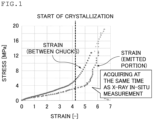
- FIG. 1 illustrates a relationship between nominal tensile strain (between chucks) and stress, a relationship between engineering strain (emitted portion) and stress of the sample of the formulation 1.
- nominal tensile strain between chucks
- engineering strain emitted portion
- FIG. 2(a) is a schematic view that schematically shows a stretching deformation mechanism when an observation image is acquired by observing the state of the sample (rubber material) in stretching using a transmission electron microscope.
- a three-dimensional TEM tensile holder 11 sample cartridge
- achieves the bidirectional drawing of the observed sample (rubber material) 12 the observed sample is drawn in opposite directions at the same time. This makes it possible to stretch the sample in a bisectional drawing manner and allows observation of the sample using TEM without misalignment of the visual field in stretching.
- a thin slice is prepared from the sample of the formulation 1 with a diamond knife and is fixed on a sample cartridge.
- the fixed thin slice is observed using TEM at various stretchings (strains).
- One example of the preparation conditions of the thin slice (observed sample) is as follows but can be appropriately changed.
- the dark section of the figure shows zinc oxide and the like, and the bright section shows a rubber matrix.
- the sample is stretched in the vertical direction in the observed visual field. Measuring the distance between the zinc oxide aggregates in each TEM image makes it possible to calculate strain in each stretching phase and the stretching rate. Because the state that the distance between the zinc oxide aggregates increases can be observed in synchronization with the motion of the three-dimensional TEM tensile holder 11, in-situ observation at various strains (observation of the corresponding portion at the stretched portion) in the stretching process of the sample can be performed without misalignment of the visual field in stretching.
- microscopic deformation for example, occurrence of nanovoids or deformation of aggregates of zin oxide particles, the same visual field observed in situ by the three-dimensional TEM tensile holder 11 is very effective.
- One example of the observation conditions of TEM in stretching is as follows but can be appropriately changed.
- the schematic view showing the void growth it is found that the void grows along the boundary of the rubber/zinc oxide in the case of low strain, and the void grows drastically when the stretching strain is a predetermined value or higher (for example, ⁇ > 2.0), which indicates that the void behaves near zinc oxide in the two-phase growth process.
- FIG. 2 FIG. 2(b)
- FIG. 2(b) is a schematic view schematically showing an apparatus including ADF-STEM and NDI for use at that time and the observation approach.
- annular dark field scanning transmission electron microscopy is used to observe an image
- the above nanodiffraction imaging technique can be used to observe the state of the crystal inside the rubber material in stretching.
- ADF-STEM is a method in which finely converged electron beams are emitted to a sample while scanned on the sample, and electrons scattered at high angles of transmitted electrons are detected by an annular detector, to display an integrated intensity of the detected electrons.
- one example of a scanning transmission electron microscope is, for example, an apparatus provided with an electron source configured to output electron beams, a converging lens configured to converge the electron beams output from the electron source, and an objective lens configured to focus the focal point of the electron beams output from the electron source to the position of the sample.
- the converging lens can converge, for example, electron beams to a nanometer level or less.
- the scanning transmission electron microscope is arranged between, for example, the electron beam source and the objective lens.
- One example of the scanning transmission electron microscope is, for example, an apparatus equipped with a scanning coil configured to scan electron beams on the surface of a sample and an image forming lens configured to allow the electron beams passing through the sample to form an image on an image surface.
- FIG. 2(b) The apparatus of FIG. 2(b) is provided with an annular dark field detector (ADF Detector) 13 arranged on the image formation plane on which a dark field image is formed and is also provided with a pixel detector 14.
- ADF Detector annular dark field detector
- FIG. 2(b) further shows that electron diffraction (ED) measurement is performed, and specifically shows that an image of microelectron diffraction ( ⁇ -ED) is acquired.
- NDI nanodiffraction imaging
- the region (2) shows the portion where the void generates
- the region (1) shows the ADF-STEM image of the portion apart from the void.
- the ⁇ -ED figure consisting of nine portions (one set) shown in FIG. 5 is the diffraction pattern (5 ⁇ 5 Bined, 100 2 nm 2 ) obtained by integrating 5 ⁇ 5 (25) patterns (pixel size: 20 ⁇ 20 nm 2 ) of each of the respective figures constituting the above nine portions (each diffraction pattern).
- an integrated region of diffraction pattern is preferably a region of 1 ⁇ 1 to 1000 ⁇ 1000 nm 2 and more preferably a region of 5 ⁇ 5 to 150 ⁇ 150 nm 2 , in terms of measurement precision.
- the integrated region is 100 ⁇ 100 nm 2 .
- One example of the emitting conditions of electron beams of the electron diffraction is as follows but can be appropriately changed.
- FIG. 6 shows a diffraction pattern (3 ⁇ 3 Bined, 300 2 nm 2 ) obtained by integrating each of the nine figures of the ⁇ -ED figure (3 ⁇ 3, 300 2 nm 2 ) at a local portion, the ⁇ -ED figure consisting of nine portions of FIG. 5 as one set. From the integrated diffraction pattern obtained from integration of the nine figures, the degree of crystallinity Xc at each of the portions can be calculated, and is calculated as 14%, 16%, 13%, 20%, respectively.
- FIG. 6 indicates that the degree of crystallinity is almost the same in the portion apart from the void, but the degree of crystallinity is high near the void.
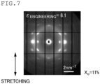
- FIG. 7 shows a diffraction pattern obtained from wide angle X-ray diffraction (WAXD) of the portion apart from the void. Since the degree of crystallinity of 11% obtained from this diffraction pattern of the WAXD and the degrees of crystallinity of 13 to 16% obtained from the ⁇ -ED of portions apart from the void in FIG. 6 almost correspond to each other, the validity of the above-described ⁇ -ED analysis can be confirmed.
- WAXD measurement conditions is as follows but can be appropriately changed.
- the present invention (1) is a method of analyzing a crystal structure, a crystal morphology, or a crystal distribution of a rubber material in stretching using a nanodiffraction imaging technique that analyzes an electron diffraction pattern acquired by scanning electron beams converged to a diameter of 100 nm or less on a surface of the rubber material while a behavior of stretching deformation of the rubber material and/or a state of the rubber material in stretching are observed using a transmission electron microscope.
- the present invention (2) is the method according to the present invention (1), wherein the nanodiffraction imaging technique is performed under measurement conditions described below:
- the present invention (3) is the method according to the present invention (1) or (2), wherein when a diffraction pattern obtained by performing a further electron diffraction is analyzed, an integrated region of the diffraction pattern is a region of 1 ⁇ 1 to 1000 ⁇ 1000 nm 2 .
- the present invention (4) is a combination method according to any one of the present inventions (1) to (3), wherein a local strain in an observation visual field of a transmission electron microscopic image is 1 to 40.
Landscapes
- Chemical & Material Sciences (AREA)
- Crystallography & Structural Chemistry (AREA)
- Physics & Mathematics (AREA)
- Health & Medical Sciences (AREA)
- Life Sciences & Earth Sciences (AREA)
- Analytical Chemistry (AREA)
- Biochemistry (AREA)
- General Health & Medical Sciences (AREA)
- General Physics & Mathematics (AREA)
- Immunology (AREA)
- Pathology (AREA)
- Analysing Materials By The Use Of Radiation (AREA)
Abstract
Description
- The present invention relates to a method of analyzing a crystal structure, a crystal morphology, or a crystal distribution of a rubber material in stretching.
- Conventionally, an approach of X-ray diffraction such as wide angle X-ray diffraction (WAXD) has been used to observe a state of a stretched crystal of an entire rubber material.
- To grasp the state of a stretched crystal of an entire sample, an approach such as X-ray diffraction may be a powerful tool. However, how the stretched crystal is locally generated and how the stretched crystal acts on cracks need to be observed in actual space.
- An object of the present invention is to solve the above problem and to provide an analysis method that can analyze a crystal structure, a crystal morphology, a crystal distribution of a rubber material in stretching even in a local portion of the rubber material.
- The present invention relates to a method of analyzing a crystal structure, a crystal morphology, or a crystal distribution of a rubber material in stretching using a nanodiffraction imaging technique that analyzes an electron diffraction pattern acquired by scanning electron beams converged to a diameter of 100 nm or less on a surface of the rubber material while a behavior of stretching deformation of the rubber material and/or a state of the rubber material in stretching are observed using a transmission electron microscope.
- The present invention is a method of analyzing a crystal structure, a crystal morphology, or a crystal distribution of a rubber material in stretching using a nanodiffraction imaging technique that analyzes an electron diffraction pattern acquired by scanning electron beams converged to a diameter of 100 nm or less on a surface of the rubber material while a behavior of stretching deformation of the rubber material and/or a state of the rubber material in stretching are observed using a transmission electron microscope. Therefore, it is possible to provide an analysis method that can analyze a crystal structure, a crystal morphology, a crystal distribution of a rubber material in stretching even in a local portion of the rubber material.
-
-
FIG. 1 is a view showing a relationship between nominal tensile strain (between chucks) and stress of a sample, a relationship between engineering strain (irradiated portion) and stress of the sample. -
FIG. 2 is a schematic view that schematically shows a stretching deformation mechanism when an observation image is acquired by observing the state of the sample in stretching using a transmission electron microscope (FIG. 2(a) ), and also a schematic view of an apparatus including annular dark field scanning transmission electron microscopy and a nanodiffraction imaging technique, as well as an observation approach (FIG. 2(b) ). -
FIG. 3 is a TEM image at the time of various strains in the stretching process of the sample. -
FIG. 4 is an enlarged view of the void (gap) portions of the TEM image ofFIG. 3 (the strain = 0, 2.4, 3.9, 6.1), and a schematic view showing the state of growing the voids. -
FIG. 5 is a view showing the state of the crystal observed by the nanodiffraction imaging technique using annular dark field scanning transmission electron microscopy in the regions (1) and (2) in the portion of 12 divisions of the stretching TEM observation image ofFIG. 3 (strain = 6.1). -
FIG. 6 is a diffraction pattern obtained by integrating each of the nine figures of the electron diffraction figure (µ-ED figure), which is obtained by emitting micron-sized electron beams to a sample at a local portion inFIG. 5 . -
FIG. 7 is a diffraction pattern obtained from wide angle X-ray diffraction at a position apart from the void (gap) . - An analysis method of the present invention is a method of analyzing a crystal structure, a crystal morphology, or a crystal distribution of a rubber material (sample) in stretching using a nanodiffraction imaging technique that analyzes an electron diffraction pattern acquired by scanning electron beams converged to a diameter of 100 nm or less on a surface of the rubber material (surface of the sample) while a behavior of stretching deformation of the rubber material (sample) and/or a state of the rubber material in stretching are observed using a transmission electron microscope.
- In an approach involving X-ray diffraction such as WAXD, it is difficult to grasp a state of a crystal of a rubber material in stretching, particularly the state of the crystal at a local portion of the rubber material in stretching.
- On the other hand, the present invention makes it possible to observe a state of a crystal with good precision even in a local portion of the rubber material in stretching by using a nanodiffraction imaging technique that analyzes an electron diffraction pattern. The electron diffraction pattern is obtained as follows. For example, a transmission electron microscope is used to observe a state of a rubber material in stretching. Then, with respect to a local portion of the thus-obtained electron microscopic image, a scanning transmission electron microscope method having atomic resolution is used to scan electron beams converged to a diameter of nanometer on the surface of the rubber material, to thereby acquire the electron diffraction pattern.
- The stretched crystal is very vulnerable to electron beam damage. When a specific amount of electron beam dose is emitted to the stretched crystal, the diffraction peak of the stretched crystal disappears. Therefore, it is important to observe the stretched crystal by emitting electron beams as weak as possible. When the following steps: observing the stretched crystal by TEM; looking for a visual field; and diffraction are performed in this order, the diffraction peak cannot be obtained due to unintentional damage of electron beam that seems to be the image observation (looking for a visual field). On the other hand, in the present invention, after the diffraction figure is acquired while electron beams are comprehensively scanned without looking for the visual field, an image is selected. Such a procedure makes it possible to simplify a procedure to look for an observation visual field to make the measured visual field larger and to select a detailed analysis visual field at the time of analyzing a diffraction pattern. As a result, it is possible to observe, with good precision, a state of a crystal even in a local portion of a rubber material in stretching, specifically, a crystal structure, a crystal morphology, a crystal distribution of the rubber material.
- Examples of the rubber material (sample) applicable to the above analysis method include samples containing a rubber component alone and samples of rubber compositions containing a rubber component and another component.
- The rubber component is not limited, and, for example, a diene rubber can be used. Examples of the diene rubber include isoprene rubber, butadiene rubber (BR), styrene-butadiene rubber (SBR), styrene-isoprene-butadiene rubber (SIBR), ethylene-propylene-diene rubber (EPDM), chloroprene rubber (CR), and acrylonitrile-butadiene rubber (NBR). In addition, for example, butyl rubber and fluororubber are also exemplified. These may be used alone or in combination.
- The rubber material (sample) may include a filler. Examples of the filler include silica, carbon black, calcium carbonate, talc, alumina, clay, aluminum hydroxide, aluminum oxide, and mica. For example, the above method can be suitably applied to a sample of a rubber composition containing silica and/or carbon black.
- The rubber material (sample) may include the rubber component and another component other than the filler. For example, the above method can be suitably applied to a sample of a rubber composition that contains at least one compounding agent generally used in a tire industry, such as a plasticizer, an antioxidant, stearic acid, wax, zinc oxide, sulfur, and a vulcanization accelerator. Particularly, in terms of measurement of the stretching rate of a sample, a sample of a rubber composition containing zinc oxide can be suitably applied. When zinc oxide is included, the stretching rate in the observation visual field of the transmission electron microscopic image can be calculated from a distance between zinc oxides, in stretching.
- The rubber material (sample) is produced by a typical method. For example, a rubber material (sample) can be produced by, for example, a method in which materials to be compounded are kneaded using a kneader such as a Banbury mixer or an open roll mill, followed by vulcanizing if necessary.
- In the above analysis method, a usable transmission electron microscope (TEM) is not limited, but a scanning transmission electron microscope (STEM) is preferably used in terms of improvement of measurement precision. In the above method, use of the transmission electron microscope makes it possible to directly observe a state of the rubber material (sample) in stretching with good precision. Among them, desirably, a TEM image at various strains (in stretching) in the stretching process of the rubber material (sample) (an image acquired by in-situ observation of the rubber material by a tensile three-dimensional TEM) is acquired, and various states of the rubber material (sample) in stretching are directly observed.
- In the above analysis method, in an observation image (transmission electron microscope image) acquired by directly observing a behavior of stretching deformation of the rubber material (sample) and/or a state of the rubber material (sample) in stretching using a transmission electron microscope, it is possible to observe the state of a crystal with good precision even in a local portion of a rubber material in stretching by using a nanodiffraction imaging technique (NDI technique), which analyzes an electron diffraction pattern acquired by scanning electron beams converged to a diameter of nanometer on a surface of the rubber material (sample surface) of a local portion in an electron microscopic image.
- When the behavior of the stretching deformation of the rubber material (sample) and/or the state of the rubber material (sample) in stretching are directly observed using the transmission electron microscope, a local strain (ε) in an observation visual field of a transmission electron microscopic image is preferably 1 or more and more preferably 2 or more, and preferably 40 or less and more preferably 20 or less.
- In the above analysis method, use of STEM having atomic resolution and use of a nanodiffraction imaging technique, which analyzes an electron diffraction (ED) pattern acquired by scanning electron beams converged to a diameter of nanometer on a surface of the rubber material using STEM, are desirable in terms of measurement precision. In the SETM-based NDI method, electron beams having a diameter of several nanometers are scanned in the order of nanometers, and an electron diffraction pattern (ED figure) or the like is acquired from each point, which makes it possible to visualize the distribution of the crystal structure in the scale of nanometers.
- The spatial resolution of the scanning transmission electron microscope is preferably less than 0.2 nm and more preferably less than 0.1 nm in terms of measurement precision. The lower limit is not limited. A smaller spatial resolution is desirable.
- For example, when the state of the crystal is observed using STEM by the NDI method, electron beams finely converged to a size of nanometers are desirably scanned on the sample in a nanometer step, to acquire an ED figure. In terms of measurement precision and reduction of damage to a sample, scanning is performed preferably in the nanometer step of 20 nm × 20 nm, and more preferably in the nanometer step of 5 nm × 5 nm.
- Regarding the NDI measurement conditions, for example, the probe size is preferably
φ 1 to φ 150 nm and more preferablyφ 1 toφ 20 nm in terms of the spatial resolution. The total dose is preferably 1.0 × 10⁻⁶ to 1.0 × 10³ e-/Å2 and more preferably 1.0 × 10⁻³ to 1.0 × 10³ e-/Å2 in terms of measurement error, analysis accuracy, and reduction of damage to a sample. Here, the total dose is a value represented by dose rate × dwell time. - Here, one example of the analysis method of the present invention will be described below but is not limited to the following method.
- As the sample (rubber material), for example, the rubber composition (vulcanized rubber composition) of the
formulation 1 represented in Table 1 is prepared.[Table 1] Blending conditions Volume percentage (%) Isoprene rubber (IR) 90.91 Stearic acid 2.27 Zinc oxide 2.73 Sulfur 2.73 Crosslinking accelerator 1.36 -
FIG. 1 illustrates a relationship between nominal tensile strain (between chucks) and stress, a relationship between engineering strain (emitted portion) and stress of the sample of theformulation 1. Here, before the stress of the sample increases, the crystallization starts. - The upper figure of
FIG. 2 (FIG. 2(a) ) is a schematic view that schematically shows a stretching deformation mechanism when an observation image is acquired by observing the state of the sample (rubber material) in stretching using a transmission electron microscope. A three-dimensional TEM tensile holder 11 (sample cartridge) achieves the bidirectional drawing of the observed sample (rubber material) 12 (the observed sample is drawn in opposite directions at the same time). This makes it possible to stretch the sample in a bisectional drawing manner and allows observation of the sample using TEM without misalignment of the visual field in stretching. - Using a cryo-ultramicrotome, a thin slice is prepared from the sample of the
formulation 1 with a diamond knife and is fixed on a sample cartridge. The fixed thin slice is observed using TEM at various stretchings (strains). One example of the preparation conditions of the thin slice (observed sample) is as follows but can be appropriately changed. -
- Cryo-ultramicrotome: cutting temperature: -160°C
- Thickness of film before stretching: 400 nm
-
FIG. 3 is a TEM image at the time of various strains (ε) in the stretching process of the sample (ε = 0, 2.4, 3.9, 6.1). The dark section of the figure shows zinc oxide and the like, and the bright section shows a rubber matrix. The sample is stretched in the vertical direction in the observed visual field. Measuring the distance between the zinc oxide aggregates in each TEM image makes it possible to calculate strain in each stretching phase and the stretching rate. Because the state that the distance between the zinc oxide aggregates increases can be observed in synchronization with the motion of the three-dimensional TEMtensile holder 11, in-situ observation at various strains (observation of the corresponding portion at the stretched portion) in the stretching process of the sample can be performed without misalignment of the visual field in stretching. Regarding microscopic deformation, for example, occurrence of nanovoids or deformation of aggregates of zin oxide particles, the same visual field observed in situ by the three-dimensional TEMtensile holder 11 is very effective. One example of the observation conditions of TEM in stretching is as follows but can be appropriately changed. -
- Resolution: 7.14 nm
- Dose amount: 6.2 × 10⁻⁴ e-/(Å2·sheet)
-
FIG. 4 is an enlarged view of the void (gap) portions of the TEM image ofFIG. 3 (the strain (ε) = 0, 2.4, 3.9, 6.1), and a schematic view showing the state of growing the voids. The enlarged view of the void portion shows that when the sample is stretched to ε = 6.1, the void generates and grows near zinc oxide. In addition, from the schematic view showing the void growth, it is found that the void grows along the boundary of the rubber/zinc oxide in the case of low strain, and the void grows drastically when the stretching strain is a predetermined value or higher (for example, ε > 2.0), which indicates that the void behaves near zinc oxide in the two-phase growth process. - In the above analysis method, the sample is observed by TEM at various strains (ε) in the stretching process, and the same time, for example, annular dark field scanning transmission electron microscopy (ADF-STEM) can be used to observe the state of the crystallization of the rubber material in stretching using the nanodiffraction imaging technique (NDI). The lower figure of
FIG. 2 (FIG. 2(b) ) is a schematic view schematically showing an apparatus including ADF-STEM and NDI for use at that time and the observation approach. Here, while annular dark field scanning transmission electron microscopy is used to observe an image, the above nanodiffraction imaging technique can be used to observe the state of the crystal inside the rubber material in stretching. ADF-STEM is a method in which finely converged electron beams are emitted to a sample while scanned on the sample, and electrons scattered at high angles of transmitted electrons are detected by an annular detector, to display an integrated intensity of the detected electrons. - In
FIG. 2(b) , one example of a scanning transmission electron microscope (STEM) is, for example, an apparatus provided with an electron source configured to output electron beams, a converging lens configured to converge the electron beams output from the electron source, and an objective lens configured to focus the focal point of the electron beams output from the electron source to the position of the sample. The converging lens can converge, for example, electron beams to a nanometer level or less. The scanning transmission electron microscope is arranged between, for example, the electron beam source and the objective lens. One example of the scanning transmission electron microscope is, for example, an apparatus equipped with a scanning coil configured to scan electron beams on the surface of a sample and an image forming lens configured to allow the electron beams passing through the sample to form an image on an image surface. - The apparatus of
FIG. 2(b) is provided with an annular dark field detector (ADF Detector) 13 arranged on the image formation plane on which a dark field image is formed and is also provided with apixel detector 14.FIG. 2(b) further shows that electron diffraction (ED) measurement is performed, and specifically shows that an image of microelectron diffraction (µ-ED) is acquired. - When the state of crystallization is observed using the ADF-STEM and the NDI method, it is possible to use the electron microscopic approach (nanodiffraction imaging, NDI) in which the acquired numerous electron diffraction patterns are analyzed while electrons finely converged to a nanometer size are scanned on the sample in a nanometer step (in
FIG. 2(b) , 20 nm × 20 nm), and the structural parameters such as the rate of crystallization are subjected to mapping at a nanometer scale. One example of the NDI measurement conditions is as follows but can be appropriately changed. -
- pixel size: 20 × 20 nm2
- probe size: φ 20 nm
- dwell time: 5.0 × 10⁻³ s
- Total dose: 8.0 e-/Å2
- pixel detector: STELA camera
- camera length: 400 mm
-
FIG. 5 shows the state of the crystal observed by the nanodiffraction imaging technique (NDI technique) using annular dark field scanning transmission electron microscopy (ADF-STEM) having atomic resolution in the regions (1) and (2) in the portion of 12 divisions (3 × 4) of the stretching TEM observation image ofFIG. 3 (strain (ε) = 6.1). The region (2) shows the portion where the void generates, and the region (1) shows the ADF-STEM image of the portion apart from the void. - Regarding two portions (local portions) in the region (1) and two portions (local portions) in the region (2), the µ-ED figure consisting of nine portions (one set) shown in
FIG. 5 is the diffraction pattern (5 × 5 Bined, 1002 nm2) obtained by integrating 5 × 5 (25) patterns (pixel size: 20 × 20 nm2) of each of the respective figures constituting the above nine portions (each diffraction pattern). - When a diffraction pattern obtained by such electron diffraction is analyzed, an integrated region of diffraction pattern is preferably a region of 1 × 1 to 1000 × 1000 nm2 and more preferably a region of 5 × 5 to 150 × 150 nm2, in terms of measurement precision. In the case of
FIG. 5 , the integrated region is 100 × 100 nm2. - The µ-ED
figure (3 × 3, 3002 nm2) at a local portion, which constitutes nine portions of one diffraction pattern (5 × 5 Bined, 1002 nm2) obtained by integrating the above 5 × 5 (25) patterns as one set, is shown. One example of the emitting conditions of electron beams of the electron diffraction is as follows but can be appropriately changed. -
- Dose rate: 2.9 × 10⁻³ e-/Å2
- Exp. time: 5.0 s
- Total dose: 0.015 e-/Å2
- beam size: φ 2.1 µm
-
FIG. 6 shows a diffraction pattern (3 × 3 Bined, 3002 nm2) obtained by integrating each of the nine figures of the µ-EDfigure (3 × 3, 3002 nm2) at a local portion, the µ-ED figure consisting of nine portions ofFIG. 5 as one set. From the integrated diffraction pattern obtained from integration of the nine figures, the degree of crystallinity Xc at each of the portions can be calculated, and is calculated as 14%, 16%, 13%, 20%, respectively.FIG. 6 indicates that the degree of crystallinity is almost the same in the portion apart from the void, but the degree of crystallinity is high near the void. - Note that,
FIG. 7 shows a diffraction pattern obtained from wide angle X-ray diffraction (WAXD) of the portion apart from the void. Since the degree of crystallinity of 11% obtained from this diffraction pattern of the WAXD and the degrees of crystallinity of 13 to 16% obtained from the µ-ED of portions apart from the void inFIG. 6 almost correspond to each other, the validity of the above-described µ-ED analysis can be confirmed. One example of the WAXD measurement conditions is as follows but can be appropriately changed. -
- Type-7 dumbbell test piece
- Beam Size: 350 × 0.400 µm2
- As described above, reconsideration of the procedure of the observation of TEM images, the diffraction measurement, and use of a nanodiffraction imaging technique that analyzes an electron diffraction pattern acquired by scanning converged electron beams on a surface of the rubber material while a state of the rubber material in stretching is observed using a transmission electron microscope (i.e., performing the procedure in which after a diffraction figure is acquired while electron beams are comprehensively scanned without looking for a visual field, an image is selected) make it possible to reduce the damage of electron beams on the sample. As a result, an electron diffraction peak of a drawn crystal can be detected and the state of crystallization of the rubber material in stretching can be analyzed.
- Particularly, in addition to in-situ TEM observation of stretching, implementation and analysis of simultaneous measurements of ADF-STEM and NDI make it possible to obtain the indication that, for example, the drawn crystal at a high strain region (ε = 6.1 etc.) has a high degree of crystallinity near a void.
- Therefore, it is believed that such an analysis method of the present invention could unravel an influence of a behavior of local deformation on the space/orientation distribution of the drawn crystal.
- The present invention (1) is a method of analyzing a crystal structure, a crystal morphology, or a crystal distribution of a rubber material in stretching using a nanodiffraction imaging technique that analyzes an electron diffraction pattern acquired by scanning electron beams converged to a diameter of 100 nm or less on a surface of the rubber material while a behavior of stretching deformation of the rubber material and/or a state of the rubber material in stretching are observed using a transmission electron microscope.
- The present invention (2) is the method according to the present invention (1),
wherein the nanodiffraction imaging technique is performed under measurement conditions described below: - (measurement conditions)
- probe size:
φ 1 to φ 150 nm - total dose: 1.0 × 10⁻⁶ to 1.0 × 10³ e-/Å2.
- The present invention (3) is the method according to the present invention (1) or (2),
wherein when a diffraction pattern obtained by performing a further electron diffraction is analyzed, an integrated region of the diffraction pattern is a region of 1 × 1 to 1000 × 1000 nm2. - The present invention (4) is a combination method according to any one of the present inventions (1) to (3),
wherein a local strain in an observation visual field of a transmission electron microscopic image is 1 to 40. -
- 11 three-dimensional TEM tensile holder (sample cartridge)
- 12 observed sample (rubber material)
- 13 annular dark field detector
- 14 pixel detector
Claims (4)
- A method of analyzing a crystal structure, a crystal morphology, or a crystal distribution of a rubber material in stretching using a nanodiffraction imaging technique that analyzes an electron diffraction pattern acquired by scanning electron beams converged to a diameter of 100 nm or less on a surface of the rubber material while a behavior of stretching deformation of the rubber material and/or a state of the rubber material in stretching are observed using a transmission electron microscope.
- The method according to claim 1,
wherein the nanodiffraction imaging technique is performed under measurement conditions described below:(measurement conditions)probe size: φ 1 to φ 150 nmtotal dose: 1.0 × 10⁻⁶ to 1.0 × 10³ e-/Å2. - The method according to claim 1 or 2,
wherein when a diffraction pattern obtained by performing a further electron diffraction is analyzed, an integrated region of the diffraction pattern is a region of 1 × 1 to 1000 × 1000 nm2. - The method according to any one of claims 1 to 3,
wherein a local strain in an observation visual field of a transmission electron microscopic image is 1 to 40.
Applications Claiming Priority (1)
| Application Number | Priority Date | Filing Date | Title |
|---|---|---|---|
| JP2023071742A JP2024157396A (en) | 2023-04-25 | 2023-04-25 | Method for analyzing crystal structure, crystal morphology, or crystal distribution of rubber material during stretching |
Publications (1)
| Publication Number | Publication Date |
|---|---|
| EP4455651A1 true EP4455651A1 (en) | 2024-10-30 |
Family
ID=90675332
Family Applications (1)
| Application Number | Title | Priority Date | Filing Date |
|---|---|---|---|
| EP24166852.4A Pending EP4455651A1 (en) | 2023-04-25 | 2024-03-27 | Method of analyzing crystal structure, crystal morphology, or crystal distribution of rubber material in stretching |
Country Status (3)
| Country | Link |
|---|---|
| US (1) | US20240361260A1 (en) |
| EP (1) | EP4455651A1 (en) |
| JP (1) | JP2024157396A (en) |
Families Citing this family (5)
| Publication number | Priority date | Publication date | Assignee | Title |
|---|---|---|---|---|
| JP2026052311A (en) * | 2024-09-11 | 2026-03-24 | サミー株式会社 | Gaming machine |
| JP2026052308A (en) * | 2024-09-11 | 2026-03-24 | サミー株式会社 | Gaming machine |
| JP2026052310A (en) * | 2024-09-11 | 2026-03-24 | サミー株式会社 | Gaming machine |
| JP2026052309A (en) * | 2024-09-11 | 2026-03-24 | サミー株式会社 | Gaming machine |
| JP2026052312A (en) * | 2024-09-11 | 2026-03-24 | サミー株式会社 | Gaming machine |
-
2023
- 2023-04-25 JP JP2023071742A patent/JP2024157396A/en active Pending
-
2024
- 2024-03-27 EP EP24166852.4A patent/EP4455651A1/en active Pending
- 2024-03-28 US US18/619,796 patent/US20240361260A1/en active Pending
Non-Patent Citations (4)
| Title |
|---|
| ANDREWS E. H.: "Microfibrillar textures in polymer fibers", JOURNAL OF POLYMER SCIENCE PART A-2: POLYMER PHYSICS, vol. 4, no. 4, August 1966 (1966-08-01), pages 668 - 672, XP093203022, ISSN: 0449-2978, Retrieved from the Internet <URL:https://onlinelibrary.wiley.com/doi/pdfdirect/10.1002/pol.1966.160040413> DOI: 10.1002/pol.1966.160040413 * |
| COWLEY J.M. ET AL: "Electron nanodiffraction", MICROSCOPY RESEARCH AND TECHNIQUE., vol. 46, no. 2, 15 July 1999 (1999-07-15), GB, pages 75 - 97, XP093203264, ISSN: 1059-910X, DOI: 10.1002/(SICI)1097-0029(19990715)46:2<75::AID-JEMT2>3.0.CO;2-S * |
| KELLER A ET AL: "Oriented crystallization in polymers", JOURNAL OF MACROMOLECULAR SCIENCE PART B. PHYSICS, MARCEL DEKKER INC., NEW YORK, NY, US, vol. 1, no. 1, 1967, pages 41 - 91, XP009182550, ISSN: 0022-2348, DOI: 10.1080/00222346708212739 * |
| TSUJI MASAKI ET AL: "TEM Studies on Thin Films of Natural Rubber and Polychloroprene Crystallized under Molecular Orientation Il. Highly Prestretched Thin Films", POLYMER JOURNAL, 2000, pages 505 - 512, XP093203046, Retrieved from the Internet <URL:https://www.nature.com/articles/pj200093.pdf> * |
Also Published As
| Publication number | Publication date |
|---|---|
| JP2024157396A (en) | 2024-11-07 |
| US20240361260A1 (en) | 2024-10-31 |
Similar Documents
| Publication | Publication Date | Title |
|---|---|---|
| US20240361260A1 (en) | Method of analyzing crystal structure, crystal morphology, or crystal distribution of rubber material in stretching | |
| Trimby | Orientation mapping of nanostructured materials using transmission Kikuchi diffraction in the scanning electron microscope | |
| Fundenberger et al. | Polycrystal orientation maps from TEM | |
| Kohjiya et al. | Three-dimensional nano-structure of in situ silica in natural rubber as revealed by 3D-TEM/electron tomography | |
| US20130167665A1 (en) | Sample observation apparatus | |
| CN116465912A (en) | A rapid non-destructive testing method for silicon carbide crystal quality | |
| CN102954975A (en) | Method for analyzing rubber compound with filler particles | |
| JP2020027084A (en) | Crosslinked structure visualization method | |
| US7427753B2 (en) | Method of cross-section milling with focused ion beam (FIB) device | |
| JP2017201252A (en) | Vulcanized material analysis method | |
| DE102023120736B3 (en) | PARTICLE MICROSCOPE SYSTEM AND METHOD FOR DETERMINING AN ARRANGEMENT OF A SAMPLE IN A PARTICLE MICROSCOPE SYSTEM | |
| JP6613637B2 (en) | Method for evaluating response characteristics of internal structure of polymer materials | |
| JP5767477B2 (en) | How to observe rubber materials | |
| Alvis et al. | High-throughput, site-specific sample prep of ultra-thin TEM lamella for process metrology and failure analysis | |
| JP2013054578A (en) | Method for simulating rubber material | |
| JP2008256560A (en) | Thin film sample and manufacturing method thereof | |
| Gutierrez-Urrutia et al. | Influence of microscope settings on dislocation imaging in transmission forescattered electron imaging (t-FSEI) | |
| US20230280256A1 (en) | Analysis method | |
| JP5767541B2 (en) | Rubber material simulation method | |
| Zhou et al. | GaN epitaxial layer dislocation characterization using ECCI and TEM | |
| CN109030496A (en) | A kind of calculation method of cubic system Dislocations Bai Shi vector along any crystal orientation projection vector | |
| JP5993218B2 (en) | How to observe rubber materials | |
| ZHAO et al. | High-resolution three-dimensional visualization of dislocations in Mo using weak-beam dark-field electron tomography | |
| JP2013044607A (en) | Method of observing rubber material | |
| Yamasaki | Observation and measurement using the Electron channeling pattern function |
Legal Events
| Date | Code | Title | Description |
|---|---|---|---|
| PUAI | Public reference made under article 153(3) epc to a published international application that has entered the european phase |
Free format text: ORIGINAL CODE: 0009012 |
|
| STAA | Information on the status of an ep patent application or granted ep patent |
Free format text: STATUS: THE APPLICATION HAS BEEN PUBLISHED |
|
| AK | Designated contracting states |
Kind code of ref document: A1 Designated state(s): AL AT BE BG CH CY CZ DE DK EE ES FI FR GB GR HR HU IE IS IT LI LT LU LV MC ME MK MT NL NO PL PT RO RS SE SI SK SM TR |
|
| P01 | Opt-out of the competence of the unified patent court (upc) registered |
Free format text: CASE NUMBER: APP_12430/2025 Effective date: 20250313 |
|
| STAA | Information on the status of an ep patent application or granted ep patent |
Free format text: STATUS: REQUEST FOR EXAMINATION WAS MADE |
|
| 17P | Request for examination filed |
Effective date: 20250429 |