EP4451833A1 - Metallplatte und abscheidungsmaske zur oled-pixelabscheidung damit - Google Patents
Metallplatte und abscheidungsmaske zur oled-pixelabscheidung damit Download PDFInfo
- Publication number
- EP4451833A1 EP4451833A1 EP22907760.7A EP22907760A EP4451833A1 EP 4451833 A1 EP4451833 A1 EP 4451833A1 EP 22907760 A EP22907760 A EP 22907760A EP 4451833 A1 EP4451833 A1 EP 4451833A1
- Authority
- EP
- European Patent Office
- Prior art keywords
- metal plate
- region
- residual stress
- waviness
- deposition mask
- Prior art date
- Legal status (The legal status is an assumption and is not a legal conclusion. Google has not performed a legal analysis and makes no representation as to the accuracy of the status listed.)
- Pending
Links
Images



Classifications
-
- C—CHEMISTRY; METALLURGY
- C23—COATING METALLIC MATERIAL; COATING MATERIAL WITH METALLIC MATERIAL; CHEMICAL SURFACE TREATMENT; DIFFUSION TREATMENT OF METALLIC MATERIAL; COATING BY VACUUM EVAPORATION, BY SPUTTERING, BY ION IMPLANTATION OR BY CHEMICAL VAPOUR DEPOSITION, IN GENERAL; INHIBITING CORROSION OF METALLIC MATERIAL OR INCRUSTATION IN GENERAL
- C23C—COATING METALLIC MATERIAL; COATING MATERIAL WITH METALLIC MATERIAL; SURFACE TREATMENT OF METALLIC MATERIAL BY DIFFUSION INTO THE SURFACE, BY CHEMICAL CONVERSION OR SUBSTITUTION; COATING BY VACUUM EVAPORATION, BY SPUTTERING, BY ION IMPLANTATION OR BY CHEMICAL VAPOUR DEPOSITION, IN GENERAL
- C23C14/00—Coating by vacuum evaporation, by sputtering or by ion implantation of the coating forming material
- C23C14/04—Coating on selected surface areas, e.g. using masks
-
- C—CHEMISTRY; METALLURGY
- C23—COATING METALLIC MATERIAL; COATING MATERIAL WITH METALLIC MATERIAL; CHEMICAL SURFACE TREATMENT; DIFFUSION TREATMENT OF METALLIC MATERIAL; COATING BY VACUUM EVAPORATION, BY SPUTTERING, BY ION IMPLANTATION OR BY CHEMICAL VAPOUR DEPOSITION, IN GENERAL; INHIBITING CORROSION OF METALLIC MATERIAL OR INCRUSTATION IN GENERAL
- C23C—COATING METALLIC MATERIAL; COATING MATERIAL WITH METALLIC MATERIAL; SURFACE TREATMENT OF METALLIC MATERIAL BY DIFFUSION INTO THE SURFACE, BY CHEMICAL CONVERSION OR SUBSTITUTION; COATING BY VACUUM EVAPORATION, BY SPUTTERING, BY ION IMPLANTATION OR BY CHEMICAL VAPOUR DEPOSITION, IN GENERAL
- C23C14/00—Coating by vacuum evaporation, by sputtering or by ion implantation of the coating forming material
- C23C14/04—Coating on selected surface areas, e.g. using masks
- C23C14/042—Coating on selected surface areas, e.g. using masks using masks
-
- H—ELECTRICITY
- H10—SEMICONDUCTOR DEVICES; ELECTRIC SOLID-STATE DEVICES NOT OTHERWISE PROVIDED FOR
- H10K—ORGANIC ELECTRIC SOLID-STATE DEVICES
- H10K50/00—Organic light-emitting devices
-
- H—ELECTRICITY
- H10—SEMICONDUCTOR DEVICES; ELECTRIC SOLID-STATE DEVICES NOT OTHERWISE PROVIDED FOR
- H10K—ORGANIC ELECTRIC SOLID-STATE DEVICES
- H10K71/00—Manufacture or treatment specially adapted for the organic devices covered by this subclass
-
- H—ELECTRICITY
- H10—SEMICONDUCTOR DEVICES; ELECTRIC SOLID-STATE DEVICES NOT OTHERWISE PROVIDED FOR
- H10K—ORGANIC ELECTRIC SOLID-STATE DEVICES
- H10K71/00—Manufacture or treatment specially adapted for the organic devices covered by this subclass
- H10K71/10—Deposition of organic active material
- H10K71/16—Deposition of organic active material using physical vapour deposition [PVD], e.g. vacuum deposition or sputtering
- H10K71/166—Deposition of organic active material using physical vapour deposition [PVD], e.g. vacuum deposition or sputtering using selective deposition, e.g. using a mask
-
- H—ELECTRICITY
- H10—SEMICONDUCTOR DEVICES; ELECTRIC SOLID-STATE DEVICES NOT OTHERWISE PROVIDED FOR
- H10K—ORGANIC ELECTRIC SOLID-STATE DEVICES
- H10K99/00—Subject matter not provided for in other groups of this subclass
Definitions
- An embodiment relates to a metal plate and a deposition mask for OLED pixel deposition.
- a display device is applied and used in various devices.
- the display device is applied and used not only in a small device such as a smartphone and a tablet PC, but also in a large device such as a TV, a monitor, and a public display (PD).
- a small device such as a smartphone and a tablet PC
- a large device such as a TV, a monitor, and a public display (PD).
- UHD ultra-high resolution
- PPI Picture Per Inch
- a high-resolution display device is being applied to a small device and a large device. Accordingly, interest in technologies for low-power and high-resolution implementation is increasing.
- Generally used display devices can be largely divided into LCD (Liquid Crystal Display) and Organic Light Emitting Diode (OLED) depending on a driving method.
- LCD Liquid Crystal Display
- OLED Organic Light Emitting Diode
- the LCD is a display device driven by using a liquid crystal, and has a structure in which a light source including a CCFL (Cold Cathode Fluorescent Lamp) or an LED (Light Emitting Diode) is disposed under the liquid crystal.
- the LCD is a display device driven by adjusting the amount of light emitted from the light source by using the liquid crystal disposed on the light source.
- the OLED is a display device driven by using an organic material and does not require a separate light source. Accordingly the OLED can be driven at low power by the organic material performing a function of the light source. In addition, the OLED can express infinite contrast ratio and have a response speed about 1000 times faster than LCD and an excellent viewing angle. Accordingly, the OLED is attracting attention as a display device that can replace LCD.
- the organic material included in a light emitting layer in the OLED may be deposited on a substrate by a deposition mask called a fine metal mask (FMM), and the deposited organic material may be formed in a pattern corresponding to a pattern formed in the deposition mask and may function as a pixel.
- the deposition mask is generally manufactured using an invar alloy metal plate including iron (Fe) and nickel (Ni). In this case, a through hole passing through one surface and the other surface is formed in the metal plate. The through hole may be formed at a position corresponding to a pixel pattern. Accordingly, organic materials such as red, green, and blue can pass through the through hole of the metal plate and be deposited on the substrate, and a pixel pattern can be formed on the substrate.
- the invar alloy metal plate used as the deposition mask can allow a through hole to be formed in the metal plate after going through a pretreatment process of modifying the thickness and a surface of the metal plate.
- a stress distribution inside the metal plate may be changed by the pretreatment process of the metal plate. Accordingly, the metal plate may be bent due to non-uniformity in the stress distribution inside the metal plate, and a waviness of the metal plate may increase.
- the deposition mask when each deposition mask is cut into an unit size after forming a through hole in a metal plate on which a pretreatment process has been performed, the deposition mask may be bent due to this stress.
- the metal plate according to an embodiment may control residual stress and waviness of the metal plate remaining after the pretreatment process within a set range, and may improve a problem of a gap between the deposition mask manufactured by the metal plate and the deposition substrate. Therefore, when the organic material is deposited on the deposition substrate through the deposition mask manufactured by the metal plate, the deposition efficiency is improved.
- first, second, A, B, (a), and (b) may be used. These terms are only used to distinguish the elements from other elements, and the terms are not limited to the essence, order, or order of the elements.
- an element when an element is described as being “connected”, “coupled”, or “contacted” to another element, it may include not only when the element is directly “connected” to, “coupled” to, or “contacted” to other elements, but also when the element is “connected”, “coupled”, or “contacted” by another element between the element and other elements.
- the "on (over)” or “under (below)” may include not only when two elements are directly connected to each other, but also when one or more other elements are formed or disposed between two elements.
- FIG. 1 is a view illustrating an organic material deposition apparatus to which a deposition mask according to an embodiment is applied.
- an organic material deposition apparatus 1000 includes a deposition mask 1100, a mask frame 1200, a deposition substrate 1300, an organic material deposition container 1400, and a vacuum chamber 1500.
- the deposition mask 1100, the mask frame 1200, the deposition substrate 1300, and the organic material deposition container 1400 are accommodated in the vacuum chamber 1500. Accordingly, a deposition process through the deposition mask 1100 may be performed in a vacuum atmosphere.
- the deposition substrate 1300 is a substrate used for manufacturing a display device.
- the deposition substrate 1300 may be an organic material deposition substrate forming an OLED pixel pattern.
- Organic material patterns of red, green, and blue are formed on the deposition substrate 1300 to form pixels that are the three primary colors of light. That is, an RGB pattern is formed on the deposition substrate 1300.
- the deposition mask 1100 is disposed on one surface of the deposition substrate 1300.
- the deposition mask 1100 is disposed on a deposition surface on which an organic material is deposited among both surfaces of the deposition substrate 1300. Also, the deposition mask 1100 is fixed by the mask frame 1200.
- the organic material passes through a through hole TH formed in the deposition mask 1100, an organic material is deposited on the deposition surface of the deposition substrate 1300, thereby forming an RGB pattern on the deposition surface of the deposition substrate 1300.
- the organic material deposition container 1400 may be a crucible. An organic material is disposed inside the crucible. A heat source and/or current are supplied to the crucible, which is the organic material deposition container 1400, in the vacuum chamber 1500. Accordingly, the organic material passes through the deposition mask 1100, and the organic material is deposited on the deposition surface of the deposition substrate 1300.
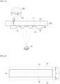
- FIG. 2 is a view for explaining an arrangement relationship between the deposition mask 1100 and the deposition substrate 1300.
- the deposition mask 1100 is disposed on a deposition surface of the deposition substrate 1300.
- the deposition mask 1100 is disposed in direct or indirect contact with the deposition surface of the deposition substrate 1300.
- the deposition mask 1100 is formed by forming a plurality of through holes THs in a metal plate 100 including iron and nickel.
- a plurality of through holes THs formed through an etching process are formed in a metal plate 100 including an invar alloy including iron and nickel to form the deposition mask 1100.
- the metal plate 100 includes a first surface 101 and a second surface 102 opposite to each other.
- a first surface hole V1 is formed at the first surface 101 of the metal plate 100
- a second surface hole V2 is formed at the second surface 102 of the metal plate 100.
- a size of the first surface hole V1 is smaller than a size of the second surface hole V2. That is, a diameter of the first surface hole V1 is smaller than a diameter of the second surface hole V2.
- the second surface hole V2 is disposed to face the organic material deposition container 1400. Accordingly, the organic material of the organic material deposition container 1400 is introduced.
- the first surface hole V1 is a region through which the organic material introduced from the second surface hole V2 passes. Accordingly, the organic material passing through the first surface hole V1 is deposited on the deposition substrate 1300.
- the first surface hole V1 and the second surface hole V2 are formed to partially pass through the metal plate 100.
- ta depth of the first surface hole V1 is smaller than a depth of the second surface hole V2.
- the first surface hole V1 and the second surface hole V2 are disposed at positions overlapping each other in a thickness direction of the metal plate 100 and are formed to communicate with each other.
- a plurality of through holes TH formed by communicating the first surface hole V1 and the second surface hole V2 are formed in the metal plate 100.
- the deposition mask 1100 is manufactured by cutting the metal plate 100 having a plurality of through-holes THs into a set unit area size.
- the deposition mask 1100 may be formed by cutting into a stick shape having a set unit area size.
- the deposition mask 1100 is disposed such that the first surface hole V1 of the deposition mask 1100 is in contact with the deposition surface of the deposition substrate 1300.
- a pretreatment process for reducing the thickness of the metal plate 100 is performed.
- a distribution of an internal stress of the metal plate that is, tensile stress and compressive stress may be changed by a pretreatment process.
- the metal plate may be bent by the change in distribution of internal stress as described above. Accordingly, a waviness of the surface of the metal plate, that is, a surface waveform may be changed.
- the bending and increase in waviness of the metal plate 100 affect a straightness of the deposition mask 1100 manufactured by the metal plate 100.
- a gap g may be formed between the deposition mask and the deposition substrate. Accordingly, the deposition efficiency of the deposition mask is deteriorated.
- a thickness of the organic material through a deposition region of the deposition mask varies depending on a region, and accordingly, there is a problem in that a thickness of the organic pattern deposited on the deposition substrate becomes non-uniform.
- FIG. 3 is a view for explaining a pretreatment process of a metal plate according to an embodiment.
- a metal plate 100 includes one surface 101 and the other surface 102 opposite to the one surface 101.
- the metal plate 100 includes iron (Fe) and nickel (Ni). Specifically, the metal plate 100 may include about 60 to 65 wt% of iron, and may include about 35 to 40 wt% of nickel. Specifically, the metal plate 100 may include about 63.5 to 64.5 wt% of iron, and may include about 35.5 to 36.5 wt% of nickel. In addition, the metal plate 100 may further include at least one element among carbon (C), silicon (Si), sulfur (S), phosphorus (P), manganese (Mn), titanium (Ti), cobalt (Co), copper (Cu), silver (Ag), vanadium (V), niobium (Nb), indium (In), and antimony (Sb) in an amount of about 1 wt% or less.
- One surface 101 and the other surface 102 of the metal plate 100 are etched.
- both surfaces of the metal plate 100 are etched through a chemical polishing process using an etching solution that may etch the metal plate 100.
- one surface 101 of the metal plate 100 is etched to have a thickness (t1) in a range of 20% to 30% of a total thickness (T) of the metal plate 100
- the other surface 102 of the metal plate 100 is etched to have a thickness t2 in a range of 20% to 30% of the total thickness T of the metal plate 100.
- the metal plate 100 includes a first surface 110 and a second surface 120 opposite to the first surface 110 by the pretreatment process.
- a thickness of the metal plate 100 is reduced by the pretreatment process.
- the metal plate 100 has a thickness t3 of 5 ⁇ m to 30 ⁇ m after the pretreatment process. More specifically, the metal plate 100 has a thickness of 15 ⁇ m to 25 ⁇ m after the pretreatment process.
- the metal plate 100 is pretreated by a chemical polishing process, it is possible to prevent the bending or waviness of the metal plate 100 generated in the pretreatment process from increasing.
- the embodiment can minimize the occurrence of residual stress inside the metal plate 100 after the pretreatment process.
- the residual stress inside the metal plate 100 after the pretreatment process may be minimized, and the waviness of the surface of the metal plate 100 may be minimized.
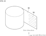
- FIGS. 4 and 5 are views for explaining a sample metal plate manufactured using a metal plate according to an embodiment.
- FIG. 6 is a view for explaining a method of measuring a residual stress of a metal plate according to an embodiment. That is, FIG. 6 is a view for describing a method of measuring residual stress of a metal plate after a pretreatment process.
- the metal plate 100 may have a thickness of about 30 ⁇ m or less as a metal plate for manufacturing the deposition mask 100 for realizing a high resolution of 400 PPI or more. Specifically, the metal plate 100 may have a thickness of about 5 ⁇ m to about 30 ⁇ m through the pretreatment process described above. More specifically, the metal plate 100 may have a thickness of about 15 ⁇ m to about 25 ⁇ m through the pretreatment process described above.
- a sample metal plate 150 having a predetermined size is separated from the metal plate 100.
- the sample metal plate 150 is a sample collected at an arbitrary point of the metal plate 100.
- the sample metal plate 150 may be at least one sample collected at an arbitrary point of the metal plate 100, and the residual stress is measured using the at least one sample.
- a sample metal plate in a form of a strip having a horizontal width greater than a vertical length is extracted at an arbitrary point of the metal plate 100. Specifically, a first sample metal plate is extracted so that a long width region has a first region as shown in FIG. 4 and a second sample metal plate is extracted so that a long width region has a second region as shown in FIG. 5 .
- the sample metal plate 150 has a set size. Specifically, a length of a first region of the first sample metal plate is X mm and a length of a second region of the first sample metal plate is Y mm. In addition, a length of the first region of the second sample metal plate is about Y mm and a length of the second region of the second sample metal plate is about X mm.
- X is 200 mm to 220 mm
- Y is 140 mm to 160 mm.
- the first sample metal plate may be a sample with a size of 210 mm*150 mm (horizontal*vertical).
- the second sample metal plate may be a sample with a size of 150 mm*210 mm (horizontal*vertical).
- the sample metal plate 150 is etched.
- one surface of the sample metal plate 150 is partially etched.
- one surface of each of the first sample metal plate and the second sample metal plate is partially etched.
- the sample metal plate 150 partially etches a region after 5% to 10% of a length of a long width region while remaining a region from one end of the long width region to 5% to 10% of the long width region of the sample metal plate 150.
- the sample metal plate 150 may be partially etched so that the thickness of the region after 5% to 10% of the long width region length of the sample metal plate 150 is about 30% to about 70% of the thickness of the sample metal plate 150.
- the sample metal plate 150 may be partially etched so that the thickness of the region after 5% to 10% of the long width region length of the sample metal plate 150 is about 50% of the thickness of the sample metal plate 150.
- the residual stress of the metal plate 100 is measured using the sample metal plate 150.
- the sample metal plate 150 is placed on a horizontal table 200 in order to measure the residual stress of the sample metal plate 150.
- the first sample metal plate and the second sample metal plate on which the above-described partial etching has been performed are placed on the horizontal table.
- the sample metal plate 150 includes one surface and the other surface.
- the sample metal plate 150 includes one surface on which partial etching has been performed and the other surface on which partial etching has not been performed.
- the sample metal plate 150 is disposed so that the other surface of the sample metal plate 150 faces an upper surface of the horizontal table 200.
- the first residual stress is a residual stress of the first sample metal plate
- the second residual stress is a residual stress of the second sample metal plate.
- the first residual stress is the residual stress of the first sample metal plate with the first region having a long width
- the second residual stress is the residual stress of the second sample metal plate with the second region having a long width
- the sample metal plate 150 mounted on the horizontal table may be bent in a region by internal stress of the metal plate and internal stress changed by the pretreatment process.
- at least one end of the etching region of the sample metal plate 150 may be bent in a region away from the upper surface of the horizontal table 200.
- at least one end of one surface of a half-etched sample metal plate 150 may be bent toward a center region of the sample metal plate 150 while being spaced apart from the upper surface of the horizontal table 200. That is, one end of the sample metal plate 150 may be bent in a region away from the horizontal table by the internal stress, and the one end may be bent in a roll shape according to a magnitude of the internal stress.
- the residual stress of the metal plate 100 is calculated by measuring a height of the partially etched region of the sample metal plate 150 spaced apart from the upper surface of the horizontal table.
- the residual stress of the metal plate 100 is defined as a maximum height at which the etched region of the sample metal plate is bent up from the upper surface of the horizontal table.
- the residual stress of the metal plate 100 can be defined by Equation 1 below.
- residual stress H/L (H is a maximum height (mm) at which an etched region of a sample metal plate is bent up from an upper surface of the horizontal table, and L is a length (mm) of a first region in which an etched region is formed in a sample metal plate)
- the metal plate 100 has a first residual stress of H/X in the first region and a second residual stress of H/Y in the second region.
- the metal plate 100 has a first residual stress of H/210 in the first region and a second residual stress of H/150 in the second region.
- the residual stress of the metal plate 100 is calculated using a plurality of sample metal plates 150.
- the first residual stress of the first sample metal plate is a value derived from an average value of a plurality of first sample metal plates measured by the method described above.
- the second residual stress of the second sample metal plate is a value derived from an average value of a plurality of second sample metal plates measured by the method described above. That is, the residual stress is an average residual stress.
- a first residual stress of a first region of the metal plate 100 and a second residual stress of the second region of the metal plate 100 are measured by the method. Specifically, the first residual stress is measured through the first sample metal plate, and the second residual stress is measured through the second sample metal plate.
- a magnitude of the first residual stress and a magnitude of the second residual stress have a set magnitude.
- the first residual stress and the second residual stress may be 10 mm or less. Specifically, the first residual stress and the second residual stress may be 7 mm or less. More specifically, the first residual stress and the second residual stress may be 5 mm or less. More specifically, the first residual stress and the second residual stress may be 1 mm to 5 mm.
- the waviness of the metal plate may increase due to the residual stress inside the metal plate. Accordingly, when the deposition mask is manufactured using the metal plate, straightness characteristics of the manufactured deposition mask may decrease.
- the magnitude of the first residual stress is different from the magnitude of the second residual stress. Specifically, the magnitude of the first residual stress is greater than the magnitude of the second residual stress.
- a ratio of the magnitude of the first residual stress and the magnitude of the second residual stress may be 1 :(0.2 to 0.7).
- a ratio of the magnitude of the first residual stress and the magnitude of the second residual stress may be 1:(0.3 to 0.6). More specifically, a ratio of the magnitude of the first residual stress and the magnitude of the second residual stress may be 1 :(0.4 to 0.5).
- the magnitude of the first residual stress may be 1 mm to 10 mm. Specifically, the magnitude of the first residual stress may be 1.5 mm to 7.5 mm. More specifically, the magnitude of the first residual stress may be 2 mm to 5 mm.
- the magnitude of the second residual stress may be 0.5 mm to 8 mm. Specifically, the magnitude of the second residual stress may be 0.5 mm to 5 mm. More specifically, the magnitude of the second residual stress may be 1 mm to 3 mm.
- the metal plate according to an embodiment may control residual stress and waviness of the metal plate remaining after the pretreatment process within a set range, and may improve a problem of a gap between the deposition mask manufactured by the metal plate and the deposition substrate. Therefore, when the organic material is deposited on the deposition substrate through the deposition mask manufactured by the metal plate, the deposition efficiency is improved.
- the metal plate according to an embodiment has a waviness in a set size range. That is, the metal plate according to an embodiment has a residual stress in a set size range. Alternatively, the metal plate according to an embodiment has a waviness in a set size range. Alternatively, the metal plate according to an embodiment has a residual stress and waviness in a set size range.
- FIG. 7 is a view illustrating a method of measuring the waviness of a metal plate according to an embodiment.
- the waviness of the metal plate is to measure the flatness of the metal plate, and may be measured using a non-contact 3D measuring device. That is, a plurality of coordinates spaced at equal intervals can be set on the metal plate, and the size of flatness can be converted to length and measured using these.
- the sample metal plate 150 having a size set in the metal plate 100 is separated to measure the waviness of the metal plate 100.
- the sample metal plate 150 is a sample collected at an arbitrary point of the metal plate 100.
- the sample metal plate 150 may be at least one sample collected at an arbitrary point of the metal plate 100, and the waviness is measured using the at least one sample.
- a sample metal plate in a form of a strip having a horizontal width greater than a vertical length is extracted at an arbitrary point of the metal plate 100. Specifically, as shown in FIG. 7 , a third sample metal plate is extracted so that a long width region has the first region.
- the sample metal plate 150 has a predetermined size. Specifically, a length of the first region of the third sample metal plate is A mm and a length of the second region is B mm. In this case, A is 490 mm to 510 mm, and B is 160 mm to 180 mm.
- the third sample metal plate may be a sample having a size of 500 mm ⁇ 170 mm (horizontal*vertical).
- a plurality of coordinates are set in the third sample metal plate. That is, a first coordinate C1, a second coordinate C2, a third coordinate C3, and a fourth coordinate C4 are set in the third sample metal plate.
- a plurality of coordinates are set inside a virtual square formed by connecting the first coordinate C1, the second coordinate C2, the third coordinate C3, and the fourth coordinate C4.
- the waviness of the metal plate 100 may be measured through a ratio of a curved distance and a straight line distance of the coordinates.
- the first waviness of the first region and the second waviness of the second region are defined by Equation 2 below.
- waviness ppm 10 6 * L ⁇ L 0 / L 0 (L is a curved distance of the coordinates, and L 0 is a straight line distance of the coordinates.)
- the waviness of the first region of the metal plate 100 is calculated based on an average value of the waviness of first virtual lines VL1 of the first region passing through the coordinates, and the waviness of the second region is calculated based on an average value of the waviness of second virtual lines VL2 of the second region passing through the coordinates.
- the first waviness of the first region of the metal plate 100 and the second waviness of the second region are measured by the method.
- a size of the first waviness and a size of the second waviness have a set size.
- the first waviness and the second waviness may be 25 ppm or less. In detail, the first waviness and the second waviness may be 20 ppm or less. In more detail, the first waviness and the second waviness may be 5 ppm to 25 ppm.
- the flatness of the surface of the metal plate is deteriorated. Accordingly, when an organic material is deposited on a deposition substrate using the deposition mask manufactured using the metal plate, a gap between the deposition mask and the deposition substrate increases, and thus the deposition efficiency may be deteriorated.
- the size of the first waviness is different from the size of the second waviness. Specifically, the size of the first waviness is larger than the size of the second waviness.
- a ratio of the size of the first waviness and the size of the second waviness may be 1 :(0.15-0.7).
- a ratio of the size of the first waviness to the size of the second waviness may be 1 :(0.2-0.6). More specifically, a ratio of the size of the first waviness and the size of the second waviness may be 1 :(0.25-0.5).
- the size of the first waviness may be 8 ppm to 25 ppm. Specifically, the size of the first waviness may be 10 ppm to 20 ppm. In more detail, the size of the first waviness may be 12 ppm to 18 ppm.
- the size of the second waviness may be 3 ppm to 25 ppm. Specifically, the size of the second waviness may be 5 ppm to 15 ppm. More specifically, the size of the second waviness may be 7 ppm to 10 ppm.
- the metal plate according to an embodiment may control residual stress and waviness of the metal plate remaining after the pretreatment process within a set range, and may improve a problem of a gap between the deposition mask manufactured by the metal plate and the deposition substrate. Therefore, when the organic material is deposited on the deposition substrate through the deposition mask manufactured by the metal plate, the deposition efficiency is improved.
- FIG. 8 is a plan view of a deposition mask according to an embodiment.
- the deposition mask 1100 includes a deposition region DA and a non-deposition region NDA.
- the deposition region DA is a region for forming a deposition pattern. That is, a deposition material is deposited on a deposition substrate through the deposition region DA through the deposition mask.
- the deposition mask 1100 includes a plurality of deposition regions DA.
- the deposition region DA includes an effective part and a non-effective part.
- the deposition region DA includes a plurality of effective parts capable of forming a deposition pattern by forming a plurality of through holes and a non-effective part UA in which no through holes are formed.
- a plurality of through holes TH described above are formed in the effective part.
- the plurality of effective parts may include a first effective part AA1, a second effective part AA2, and a third effective part AA3 spaced apart from each other by separation regions IA1 and IA2.
- any one effective part of a plurality of deposition regions included in the deposition mask 1100 may be for forming one display device.
- a plurality of effective parts included in one deposition mask 1100 may be a portion for forming one display device. Accordingly, one deposition mask 1100 may include a plurality of effective parts, and thus a plurality of display devices may be simultaneously formed. Accordingly, the deposition mask 1100 according to an embodiment may improve process efficiency.
- the non-deposition region NDA is disposed at both sides of a length region of the deposition region DA. That is, the non-deposition region NDA is disposed outside the length region of the deposition region DA.
- the non-deposition region NDA is a region that is not involved in deposition.
- the non-deposition region NDA includes a frame fixing region FA1 and FA2 for fixing the deposition mask 1100 to the mask frame 1200.
- the non-deposition region NDA includes half etching parts HF1 and HF2, open parts OA1 and OA2, and protrusion parts PA1 and PA2.
- the deposition mask 1100 according to an embodiment is manufactured by the metal plate 100 described above. Accordingly, since the metal plate for manufacturing the deposition mask has low residual stress and waviness, straightness and total pitch (T/P) characteristics of the deposition mask manufactured thereby are also improved.
- FIG. 9 is a view for explaining a straightness and a total pitch (T/P) of the deposition mask 1100 according to an embodiment.
- a deposition mask 1100 before and after bending is illustrated.
- the straightness and the total pitch of the deposition mask 1100 are calculated by a difference in positions of the deposition mask 1100 before and after bending.
- the straightness of the deposition mask 1100 is measured to be the degree of bending of the deposition mask.
- the straightness of the deposition mask 1100 is measured based on the degree of bending of the deposition mask after bending when the degree of bending of the deposition mask before bending is set to 0.
- the straightness of the deposition mask 1100 is measured based on a maximum degree of bending of the deposition mask after bending when the degree of bending of the deposition mask before bending is set to 0.
- the deposition mask 1100 manufactured using the metal plate 100 may have a straightness size of less than 50 ⁇ m. That is, the maximum bending size of the deposition mask 1100 may be less than 50 ⁇ m. Specifically, the deposition mask 1100 manufactured using the metal plate 100 may have a straightness size of 40 ⁇ m or less. In more detail, the deposition mask 1100 manufactured using the metal plate 100 may have a straightness of 15 ⁇ m to 40 ⁇ m. In more detail, the deposition mask 1100 manufactured using the metal plate 100 may have a straightness of 25 ⁇ m to 35 ⁇ m.
- the total pitch is measured based on a difference between a length of an upper surface and a length of a lower surface of the deposition mask along a major axis or a minor axis region.
- the deposition mask 1100 manufactured using the metal plate 100 may have a total pitch size of less than 30 ⁇ m. Specifically, the deposition mask 1100 manufactured using the metal plate 100 may have a total pitch size of 20 ⁇ m or less. In more detail, the deposition mask 1100 manufactured using the metal plate 100 may have a total pitch of 15 ⁇ m to 25 ⁇ m.
- the deposition mask according to the embodiment is manufactured using a metal plate with reduced residual stress and waviness. Accordingly, the straightness characteristics and total pitch characteristics of the deposition mask manufactured from the metal plate can be improved. In detail, the straightness and total pitch of deposition marks can be reduced.
- the deposition mask according to an embodiment has a reduced warpage. Therefore, when the deposition mask and the deposition substrate contact each other, the gap between the deposition region of the deposition mask and the deposition substrate may be minimized.
- the deposition mask according to the embodiment can improve deposition efficiency by minimizing the gap between the deposition mask and the deposition substrate, thereby minimizing non-uniformity in the deposition thickness.
- a separate tensile process to reduce the waviness of the above deposition mask may be omitted after forming the above deposition mask.
Landscapes
- Chemical & Material Sciences (AREA)
- Engineering & Computer Science (AREA)
- Manufacturing & Machinery (AREA)
- Chemical Kinetics & Catalysis (AREA)
- Materials Engineering (AREA)
- Mechanical Engineering (AREA)
- Metallurgy (AREA)
- Organic Chemistry (AREA)
- Physics & Mathematics (AREA)
- Optics & Photonics (AREA)
- Electroluminescent Light Sources (AREA)
- Physical Vapour Deposition (AREA)
Applications Claiming Priority (2)
| Application Number | Priority Date | Filing Date | Title |
|---|---|---|---|
| KR1020210178252A KR20230089671A (ko) | 2021-12-14 | 2021-12-14 | 금속판 및 이를 포함하는 oled 화소 증착을 위한 증착용 마스크 |
| PCT/KR2022/018858 WO2023113291A1 (ko) | 2021-12-14 | 2022-11-25 | 금속판 및 이를 포함하는 oled 화소 증착을 위한 증착용 마스크 |
Publications (2)
| Publication Number | Publication Date |
|---|---|
| EP4451833A1 true EP4451833A1 (de) | 2024-10-23 |
| EP4451833A4 EP4451833A4 (de) | 2026-04-08 |
Family
ID=86773055
Family Applications (1)
| Application Number | Title | Priority Date | Filing Date |
|---|---|---|---|
| EP22907760.7A Pending EP4451833A4 (de) | 2021-12-14 | 2022-11-25 | Metallplatte und abscheidungsmaske zur oled-pixelabscheidung damit |
Country Status (5)
| Country | Link |
|---|---|
| EP (1) | EP4451833A4 (de) |
| JP (1) | JP2024544275A (de) |
| KR (1) | KR20230089671A (de) |
| CN (1) | CN118542098A (de) |
| WO (1) | WO2023113291A1 (de) |
Family Cites Families (8)
| Publication number | Priority date | Publication date | Assignee | Title |
|---|---|---|---|---|
| KR102528582B1 (ko) * | 2015-04-24 | 2023-05-04 | 엘지이노텍 주식회사 | 금속기판 및 이를 이용한 증착용마스크 |
| US10538838B2 (en) * | 2015-09-30 | 2020-01-21 | Dai Nippon Printing Co., Ltd. | Deposition mask, method of manufacturing deposition mask and metal plate |
| KR102517596B1 (ko) * | 2017-11-21 | 2023-04-05 | 엘지이노텍 주식회사 | 증착용 마스크용 금속판의 잔류 응력 측정 방법 및 잔류 응력 특성이 개선된 증착용 마스크용 금속판 |
| CN112981319B (zh) * | 2017-09-15 | 2022-12-20 | 凸版印刷株式会社 | 蒸镀掩模、带玻璃基板的蒸镀掩模及带玻璃基板的掩模片材 |
| KR102380299B1 (ko) * | 2019-03-15 | 2022-03-29 | 도판 인사츠 가부시키가이샤 | 증착 마스크의 제조 방법, 표시 장치의 제조 방법, 및, 증착 마스크 중간체 |
| JP6788852B1 (ja) * | 2019-10-08 | 2020-11-25 | 大日本印刷株式会社 | 金属板の製造方法 |
| KR102187007B1 (ko) * | 2020-02-26 | 2020-12-04 | 주식회사 핌스 | 평탄도가 개선된 박막 증착용 마스크 조립체 및 그 제조 방법 |
| KR20210038528A (ko) * | 2021-03-31 | 2021-04-07 | 엘지이노텍 주식회사 | Oled 화소 증착을 위한 금속재의 증착용 마스크 및 이의 제조방법 |
-
2021
- 2021-12-14 KR KR1020210178252A patent/KR20230089671A/ko active Pending
-
2022
- 2022-11-25 JP JP2024535555A patent/JP2024544275A/ja active Pending
- 2022-11-25 EP EP22907760.7A patent/EP4451833A4/de active Pending
- 2022-11-25 CN CN202280088796.3A patent/CN118542098A/zh active Pending
- 2022-11-25 WO PCT/KR2022/018858 patent/WO2023113291A1/ko not_active Ceased
Also Published As
| Publication number | Publication date |
|---|---|
| CN118542098A (zh) | 2024-08-23 |
| KR20230089671A (ko) | 2023-06-21 |
| EP4451833A4 (de) | 2026-04-08 |
| JP2024544275A (ja) | 2024-11-28 |
| WO2023113291A1 (ko) | 2023-06-22 |
Similar Documents
| Publication | Publication Date | Title |
|---|---|---|
| KR102642138B1 (ko) | 증착용 마스크 및 이의 제조 방법 | |
| KR20230170628A (ko) | Oled 화소 증착을 위한 금속 재질의 증착용 마스크 및 oled 패널 제조 방법 | |
| KR102763329B1 (ko) | 증착용 마스크용 금속판의 잔류 응력 측정 방법 및 잔류 응력 특성이 개선된 증착용 마스크용 금속판 | |
| KR102516817B1 (ko) | Oled 화소 증착을 위한 금속 재질의 증착용 마스크 및 oled 패널 제조 방법 | |
| KR102716588B1 (ko) | 증착용 마스크 | |
| KR20240132432A (ko) | 증착용 마스크 및 이의 제조 방법 | |
| KR102361452B1 (ko) | Oled 화소 증착을 위한 금속 재질의 증착용 마스크 및 oled 패널 제조 방법 | |
| KR102878401B1 (ko) | 합금 금속판 및 이를 포함하는 증착용 마스크 | |
| KR20260015338A (ko) | Oled 증착 마스크용 금속 기판 및 oled 증착용 마스크 | |
| KR102927690B1 (ko) | Oled 화소 증착을 위한 금속 재질의 증착용 마스크 | |
| EP4451833A1 (de) | Metallplatte und abscheidungsmaske zur oled-pixelabscheidung damit | |
| KR102776431B1 (ko) | 합금 금속판 및 이를 포함하는 증착용 마스크 | |
| EP4577023A1 (de) | Abscheidungsmaske für oled-pixelabscheidung | |
| JP7690030B2 (ja) | Oled画素蒸着のための蒸着用マスク | |
| KR102764176B1 (ko) | 금속판 및 이를 포함하는 증착용 마스크 | |
| KR20210094833A (ko) | Oled 화소 증착을 위한 금속 재질의 증착용 마스크 | |
| KR20250091156A (ko) | Oled 화소 증착을 위한 금속 재질의 증착용 마스크 및 oled 패널 제조 방법 | |
| KR20240167225A (ko) | 금속판 및 이를 포함하는 증착용 마스크 | |
| KR20230103489A (ko) | Oled 화소 증착을 위한 증착용 마스크 | |
| KR20240112052A (ko) | 금속판 및 이를 포함하는 증착용 마스크 | |
| KR20200033600A (ko) | Oled 화소 증착을 위한 금속판 재질의 증착용 마스크 및 이의 제조방법 |
Legal Events
| Date | Code | Title | Description |
|---|---|---|---|
| STAA | Information on the status of an ep patent application or granted ep patent |
Free format text: STATUS: THE INTERNATIONAL PUBLICATION HAS BEEN MADE |
|
| PUAI | Public reference made under article 153(3) epc to a published international application that has entered the european phase |
Free format text: ORIGINAL CODE: 0009012 |
|
| STAA | Information on the status of an ep patent application or granted ep patent |
Free format text: STATUS: REQUEST FOR EXAMINATION WAS MADE |
|
| 17P | Request for examination filed |
Effective date: 20240611 |
|
| AK | Designated contracting states |
Kind code of ref document: A1 Designated state(s): AL AT BE BG CH CY CZ DE DK EE ES FI FR GB GR HR HU IE IS IT LI LT LU LV MC ME MK MT NL NO PL PT RO RS SE SI SK SM TR |
|
| DAV | Request for validation of the european patent (deleted) | ||
| DAX | Request for extension of the european patent (deleted) | ||
| A4 | Supplementary search report drawn up and despatched |
Effective date: 20260309 |
|
| RIC1 | Information provided on ipc code assigned before grant |
Ipc: H10K 99/00 20230101AFI20260303BHEP Ipc: H10K 71/00 20230101ALI20260303BHEP Ipc: C23C 14/04 20060101ALI20260303BHEP Ipc: H10K 50/00 20230101ALI20260303BHEP Ipc: H10K 71/16 20230101ALI20260303BHEP |