EP4451818A1 - Systeme und verfahren zur emi-abschirmung - Google Patents
Systeme und verfahren zur emi-abschirmung Download PDFInfo
- Publication number
- EP4451818A1 EP4451818A1 EP23168584.3A EP23168584A EP4451818A1 EP 4451818 A1 EP4451818 A1 EP 4451818A1 EP 23168584 A EP23168584 A EP 23168584A EP 4451818 A1 EP4451818 A1 EP 4451818A1
- Authority
- EP
- European Patent Office
- Prior art keywords
- shield
- electrical
- circuit
- spring
- spring elements
- Prior art date
- Legal status (The legal status is an assumption and is not a legal conclusion. Google has not performed a legal analysis and makes no representation as to the accuracy of the status listed.)
- Pending
Links
Images



Classifications
-
- H—ELECTRICITY
- H05—ELECTRIC TECHNIQUES NOT OTHERWISE PROVIDED FOR
- H05K—PRINTED CIRCUITS; CASINGS OR CONSTRUCTIONAL DETAILS OF ELECTRIC APPARATUS; MANUFACTURE OF ASSEMBLAGES OF ELECTRICAL COMPONENTS
- H05K9/00—Screening of apparatus or components against electric or magnetic fields
- H05K9/0007—Casings
- H05K9/0015—Gaskets or seals
- H05K9/0016—Gaskets or seals having a spring contact
-
- H—ELECTRICITY
- H05—ELECTRIC TECHNIQUES NOT OTHERWISE PROVIDED FOR
- H05K—PRINTED CIRCUITS; CASINGS OR CONSTRUCTIONAL DETAILS OF ELECTRIC APPARATUS; MANUFACTURE OF ASSEMBLAGES OF ELECTRICAL COMPONENTS
- H05K9/00—Screening of apparatus or components against electric or magnetic fields
- H05K9/0073—Shielding materials
- H05K9/0081—Electromagnetic shielding materials, e.g. EMI, RFI shielding
- H05K9/0088—Electromagnetic shielding materials, e.g. EMI, RFI shielding comprising a plurality of shielding layers; combining different shielding material structure
-
- H—ELECTRICITY
- H05—ELECTRIC TECHNIQUES NOT OTHERWISE PROVIDED FOR
- H05K—PRINTED CIRCUITS; CASINGS OR CONSTRUCTIONAL DETAILS OF ELECTRIC APPARATUS; MANUFACTURE OF ASSEMBLAGES OF ELECTRICAL COMPONENTS
- H05K9/00—Screening of apparatus or components against electric or magnetic fields
- H05K9/0007—Casings
- H05K9/002—Casings with localised screening
- H05K9/0022—Casings with localised screening of components mounted on printed circuit boards [PCB]
- H05K9/0024—Shield cases mounted on a PCB, e.g. cans or caps or conformal shields
-
- H—ELECTRICITY
- H05—ELECTRIC TECHNIQUES NOT OTHERWISE PROVIDED FOR
- H05K—PRINTED CIRCUITS; CASINGS OR CONSTRUCTIONAL DETAILS OF ELECTRIC APPARATUS; MANUFACTURE OF ASSEMBLAGES OF ELECTRICAL COMPONENTS
- H05K9/00—Screening of apparatus or components against electric or magnetic fields
- H05K9/0073—Shielding materials
- H05K9/0081—Electromagnetic shielding materials, e.g. EMI, RFI shielding
- H05K9/0084—Electromagnetic shielding materials, e.g. EMI, RFI shielding comprising a single continuous metallic layer on an electrically insulating supporting structure, e.g. metal foil, film, plating coating, electro-deposition, vapour-deposition
Definitions
- Radar has been used to assist various vehicle functions such as, for example, collision avoidance, cruise or flight control, and the positioning and movement of objects. Radar works by emitting high-frequency radio waves and measuring the reflection, or echo, of the waves from illuminated objects. The time delay between the transmission and reception of the waves is used to determine the distance, speed, and direction of the object. This information is processed by the vehicle's onboard computer to provide real-time information to enhance vehicle navigation and safety.
- Radar systems typically include circuits for amplifying and/or converting radar signals for transmission and/or for reception. These circuits include, for example, MMICs (monolithic microwave integrated circuits). MMICs are a type of integrated circuit operating at microwave frequencies, typically between 1 GHz and 100 GHz, and are designed to perform a variety of functions such as amplification, mixing, filtering, and signal generation.
- MMICs monolithic microwave integrated circuits
- EMI electromagnetic fields
- MMICs operate at microwave frequencies, they can generate high frequency electromagnetic fields that can interfere (EMI) with other electronic devices and systems. If not properly managed, EMI can lead to performance degradation, communication errors, and even system failure. What is desired are systems and methods that address these and other issues related to EMI.
- the extensions can flex and/or compress to maintain contact with the circuit board reference circuit even though the circuit board may exhibit irregularities. These irregularities can include, for example, bending or warping of the circuit board due to, for instance, the circuit board being large in size.
- the widths of the gaps and the distance between the extensions can be tailored to the frequency of electromagnetic radiation intended to be shielded.
- the shielding is provided by the shield being made of or having a conductive material (e.g., metal) and its one or more extensions contacting the reference voltage of the emitting circuits.
- a mask wherein the shield and electrical circuit reside within a cavity of the mask.
- the mask can be made of metal material or a material having metal (e.g., therein and/or a coating and/or layer) and can be in electrical communication with the shield (e.g., via direct or indirect contact with one or more portions of the shield).
- a thermal interface material may be provided to transfer heat away from the electric circuit.
- the TIM can be placed between the electric circuits packages and the mask, in which case the shield includes an opening or aperture through which the TIM material or layer extends to contact the mask on one side and the electric circuits packages on the other.
- the TIM material or layer can be in direct contact by having a top portion of the shield positioned between the TIM material or layer and the electric circuit.
- an electrical system having a printed circuit board and a shield.
- the printed circuit board includes an electric circuit that emits electro-magnetic radio frequency emissions.
- the shield has, for example, a top portion and a plurality of side portions connected to the top portion and surrounding the electric circuit, this shield in addition to the printed circuit board copper creates a substantially three hundred and sixty degrees confinement zone for the electromagnetic energy.
- the plurality of side portions include, for example, one or more spring contacts and one or more gaps, wherein the gaps are disposed between the spring contacts. And, the one or more spring contacts have, for example, a compressed state when contacting a reference circuit of the printed circuit board.
- a radar system having a printed circuit board and a metal shield.
- the printed circuit board includes a microwave radar circuit having electro-magnetic radio frequency emissions.
- the metal shield has, for example, a top portion and a perimeter connected to the top portion and at least partially surrounding the circuit.
- the perimeter includes, for example, one or more spring elements and one or more gaps, wherein the gaps are disposed between the spring elements.
- the one or more spring elements having, for example, a bent position when contacting a reference circuit of the printed circuit board.
- a method of forming a shielded electrical circuit includes, for example, providing a printed circuit board having a circuit that generates electro-magnetic radio frequency emissions, and placing a metal shield on the circuit board.
- the step of placing a metal shield on the circuit board includes, for example, compressing one or more spring elements of the metal shield thereby placing the one or more spring elements in contact with the reference voltage of the circuits.
- the step of compressing one or more spring elements can include, for example, bending the one or more spring elements.
- the method can further include, for example, securing the metal shield on the circuit board by placing the metal shield within a cavity of a conductive mask layer of the printed circuit board.
- the term "or” is intended to mean an inclusive “or” rather than an exclusive “or.” That is, unless specified otherwise, or clear from the context, the phrase “X employs A or B” (or other similar phrases) is intended to mean any of the natural inclusive permutations. That is, the phrase “X employs A or B” is satisfied by any of the following instances: X employs A; X employs B; or X employs both A and B.
- the articles “a” and “an” as used in this application and the appended claims should generally be construed to mean “one or more” unless specified otherwise or clear from the context to be directed to a singular form.
- top and bottom or “upper” and “lower,” are used herein for identification purposes.
- first,” second “third,” etc. are used herein for identification purposes. It is contemplated that components disclosed herein can be oriented in substantially any manner consistent with the disclosure. For instance, a top surface need not be above a bottom surface, unless specifically identified in that spatial relationship by the disclosure. Similarly, a “first” component need not come before a “second” or “third” component. Further, as used herein, the term “exemplary” is intended to mean “serving as an illustration or example of something.”
- Embodiments of the present disclosure provide systems and methods for EMI shielding that include, for example, a shield having one or more flexible or spring like extensions and gaps between the extensions.
- the flexible or spring like extensions have the ability to compress or bend via spring pressure or force. This allows the extensions to accommodate irregularities in printed circuit boards (e.g., like bending or warping) so contact is maintained with an electrical reference circuit of the printed circuit board thereby providing effective and continuous EMI shielding compared to other shielding arrangements.
- the EMI shield can also be used as a heat transfer mechanism allowing heat generated by an electrical circuit to be transferred away from the circuit.
- the EMI shield can be made from a metal material thereby providing long-term stability versus creeping and/or aging and allows for mass production at low costs. In other embodiments, the EMI shield can be made from a material having a conductive outer coating.
- FIG. 1 is a block diagram illustrating one embodiment of a system and method 100 for EMI shielding.
- the system and method can be used with any arrangement where EMI shielding is required.
- a printed circuit board (PCB) 102 is provided having one or more electrical circuits 104, which can be MMICs or other circuits that emit electromagnetic radio waves 106 during operation.
- System 100 also includes one or more EMI shields 108, examples of which will be described hereinafter.
- EMI shield 108 is connected to the reference voltage of the EMI emitting circuits of the PCB 102. Radio waves 106 are received by EMI shield 108 connected to the reference voltage, thereby preventing radio waves 106 from being emitted outside of EMI shield 108.
- Figure 1 shows by way of example a plurality of EMI shields 108 and electrical circuits 104. In other embodiments, a single EMI shield 108 and a single electrical circuit 104 can be provided on the PCB 102.
- FIG. 2 illustrates a perspective view of one embodiment of an EMI shield 108.
- EMI shield 108 includes, for example, a top portion 200 and a plurality of side portions 202, 204, 206, and 208.
- One or more of the side portions include, for example, one or more extensions (or spring contacts and/or spring elements) 210 and one or more gaps 212.
- the flexible or spring-like extensions 210 have the ability to compress or bend under a spring pressure or force.
- top portion 200 includes an opening and/or aperture 214 allowing access to the inner shielded space or volume created by EMI shield 108.
- top portion 200 need not include such an aperture/opening and may be a continuous surface (e.g., see Figures 13 , 16 , and 20 ).
- EMI shield 108 is arranged so that at least side portions 204-208 form a perimeter around the electrical circuit to which the EMI shielding is applied.
- Figures 3 and 4 illustrate perspective views of other embodiments of EMI shield 108.
- side portions 204-208 include varying numbers of extensions or spring contacts/elements.
- side portions 204 and 208 have a single extension or spring contact/element 300, 302 while side portions 202 and 206 include a plurality of extensions or spring contacts/elements 210.
- side portions 204 and 208 include a plurality of extensions or spring contacts/elements 210 while side portions 202 and 206 include a single extension or spring contact/element 400, 402.
- These embodiments are meant to be illustrative and any number of flexible extensions or spring contacts/elements can be provided in each of side portions 202-208.
- the number of flexible extensions or spring contacts/elements does not have to be equal with respect to opposing side portions (e.g., 202 and 206) or any other side portion.
- FIGS 5A and 5B illustrate cross-sectional views of one embodiment of an extension or spring contact/element 210 in its uncompressed and compressed state making contact with an electrical reference circuit/layer or contact pad 506.
- flexible extension or spring contact 210 can include, for example, a body 500 having the plurality of sections or portions 502 and 504.
- the plurality of sections 502 and 504 can be bent with respect to each other to form, for example, the arrangement shown in Figure 5A .
- more or less sections than that shown can be included.
- Portion 502 can be, for example, an elongate section extending from top portion 200 and forming a first angle A1 therebetween representing an uncompressed configuration.
- Portion 504 can be, for example, a contact portion for making contact with reference voltage of the circuits 506 of PCB 102.
- Contact portion 504 can have the same or different dimensions compared to elongate section 502. Generally, contact portion 504 is sized and dimensioned to provide effective contact with reference circuit/pad 506 in PCB 102.
- extension or spring element 210 is shown in its compressed state making contact with reference circuit/pad 506.
- compressive force(s) F1 and F2 are applied to extension or spring element 210.
- This force can, for example, be applied during PCB 102 assembly and applied via/through an EMI mask/radome (e.g., see Figures 8 , 14-15, and 16 ) or other component(s).
- EMI mask/radome e.g., see Figures 8 , 14-15, and 16
- extension or spring element 210 is flexible/compressible, it will bend/flex/compress under the applied forces. In this state, the angle A2 top portion 200 and extension or spring element 210 will be different from the uncompressed angle A1.
- compressed angle A2 will be greater than uncompressed angle A1 due to the flexing or bending of extension or spring element 210.
- this flexing/bending/compression allows extension or spring element 210 to maintain contact with the reference voltage of the circuits 506 even though the PCB 102 may be bent or warped instead of flat or planar (or may have started planar and become bent or warped over time).
- the EMI shield 108 continues to provide effective EMI shielding by not losing contact with the reference voltage of the circuits 506 of the PCB 102 even though irregularities may exist in PCB 102 and/or EMI shield itself.
- Figure 6 illustrates one embodiment of an extension or spring contact/element 210 having a pitch distance "d" and gaps 212 having a width "w.”
- gap 212 has an approximate width according to the following: w ⁇ ⁇ / 30 wherein w comprises the approximate gap width and ⁇ comprises the wavelength of the electromagnetic radiation to be shielded.
- Other formulas can also be used.
- gap 212 width w can be less than ⁇ / x where x can be a number value larger or smaller than 30.
- the gap width w should be less than the electromagnetic wavelength ⁇ to be shielded.
- Extension or spring element 210 has an approximate pitch according to the following: d ⁇ n ⁇ 4 wherein d comprises an approximate pitch length, n comprises an integer greater than zero (0), and ⁇ comprises the wavelength of electromagnetic radiation to be shielded.
- d comprises an approximate pitch length
- n comprises an integer greater than zero (0)
- ⁇ comprises the wavelength of electromagnetic radiation to be shielded.
- FIG. 7 illustrates an exploded perspective view of another embodiment of a system and method for EMI shielding.
- PCB 102 is provided with EMI shield 108 surrounding an electric circuit such as, for example, an MMIC.
- a thermal interface material (TIM) layer 700 can be included on the MMIC to facilitate heat transfer away from the electric circuit.
- PCB 102 includes an optional alignment feature 706, such as one or more guide pins, clips, or similar devices to properly align EMI shield 108 on the PCB 102 so that EMI shield 108 contacts the reference voltage of the circuits of the PCB 102.
- a mask 702 is shown removed above the PCB 102.
- Mask 702 includes a cavity or space 704 for EMI shield 108 (and electric circuit).
- Mask 702 can be a variety of materials including, for example, a layer of conductive material applied over the surface of an PCB, EMI Shield, and/or MMIC, or other electronic components. Mask 702 can cover the active area of the component, while optionally leaving other components exposed such as, for example, contacts, bond pads, antennas, etc. Mask 102 can be made from a material that is metal such as, for example, aluminum, copper and/or other conductive material. In operation, mask 702 generally assists in reducing EMI and its exact arrangement can vary based on the specific requirements and design of the component being shielded. As will be shown and described, mask 702 is applied to PCB 102 in a manner that protects and shields components on PCB 102.
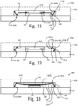
- Figures 8-13 illustrate cross-sectional views of embodiments of the systems and methods for EMI shielding having various arrangements of extension or spring elements 210, 300.
- Figure 8 illustrates an embodiment 800 where extension or spring element 210, 300 has various bent sections 802 and 806 forming a downward facing hook-like shape.
- a bend or junction 804 is between sections 802 and 804.
- compressive forces F 1 and/or F2 are applied to EMI shield 108, one or more of sections 802 and 806 bend or deflect at junction 804 in a spring-like manner to contact the reference circuit/ pads of PCB 102.
- Figure 9 illustrates an embodiment 900 where extension or spring element 210, 300 has various bent sections 904 and 908 forming an upward facing hook-like shape.
- a bend or junction 906 is between sections 904 and 908.
- compressive forces similar to F1 and/or F2 of Figure 8
- section 904 bends or deflects at junction 902 in a spring-like manner to contact the reference voltage of the circuits of PCB 102.
- sections 904 and 908 may also bend or deflect at junction 906 in a spring-like manner.
- Figure 10 illustrates an embodiment 1000 where extension or spring element 210, 300 has various bent sections 1004, 1008 and 1012 forming a downward facing hook-like shape.
- a plurality of bends or junctions 1002, 1006 and 1010 are provided between the bent sections.
- section 1004 bends or deflects at junction 1002 in a spring-like manner to contact the reference voltage of the circuits of PCB 102.
- sections 1008 and 1012 may also bend or deflect at junctions 1006 and/or 1010 in a spring-like manner.
- Figure 11 illustrates an embodiment 1100 where extension or spring element 210, 300 has various bent sections 1104, 1108 and 1112 forming an upward facing hook-like shape.
- a plurality of bends or junctions 1102, 1106 and 1110 are provided between the bent sections.
- compressive forces similar to F1 and/or F2 of Figure 8
- one or more of sections 1104, 1108 and/or 1112 bend or deflect at junctions 1102, 1106 and/or 1110 in a spring-like manner to contact the reference voltage of the circuits of PCB 102.
- Figure 12 illustrates an embodiment 1200 where extension or spring element 210, 300 has various bent sections 1204, 1208 and 1212 forming a downward facing hook-like shape. A plurality of bends or junctions 1202, 1206 and 1210 are provided between the bent sections. When compressive forces (similar to F1 and/or F2 of Figure 8 ) are applied to EMI shield 108, one or more of sections 1204, 1208 and/or 1212 bend or deflect at junctions 1202, 1206 and/or 1210 in a spring-like manner to contact the reference voltage of the circuits of PCB 102.
- compressive forces similar to F1 and/or F2 of Figure 8
- Figure 13 illustrates an embodiment 1300 of an EMI shield 108 having a planar top portion 1302 and where extension or spring elements 210, 300 have various bent sections 1308, 1312 and 1316 forming a downward facing hook-like shape. A plurality of bends or junctions 1306, 1310 and 1314 are provided between the bent sections. When compressive forces (similar to F1 and/or F2 of Figure 8 ) are applied to EMI shield 108, one or more of sections 1308, 1312 and/or 1316 bend or deflect at junctions 1306, 1310, and/or 1314 in a spring-like manner to contact the reference voltage of the circuits of PCB 102.
- compressive forces similar to F1 and/or F2 of Figure 8
- the embodiment of Figure 13 also optionally includes a thermal interface grease layer 1304 between the electrical circuit 104 and the top portion 1302 of EMI shield 108.
- Planar top portion 1302 is between thermal interface grease layer 1304 and TIM layer 700 thus providing a thermal path to cool the electric circuit 104.
- thermal interface grease 1304 can be compressed to accommodate the compressive forces applied to EMI shield 108.
- Use of thermal interface grease improves thermal contact and compensates for surface roughness of the components.
- a larger TIM layer 700 can be used that extends between the bending parts (e.g., extensions 201, 300) of EMI shield 108 compared to other embodiments.
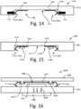
- Figures 14 and 15 illustrate cross-sectional views of various embodiments of EMI shields 108 preassembled with molded or milled EMI masks 702 and prior to association with PCB 102.
- an embodiment 1400 is shown having EMI shield 108 within cavity 704 and retained therein via radially compressive forces F3 and F4 created by the side walls of cavity 704.
- an alternate embodiment 1500 is shown having EMI shield 108 within cavity 704 and kept therein via retainers 1502.
- Retainers 1502 can be, for example, fasteners such as aluminum or copper rivets or other rivet-like structures having a body and wider head portion, as shown.
- extensions 210, 300 can extend beyond the body of mask 702 and then compress or flex as they contact the voltage reference of the circuits of PCB 102 during assembly therewith.
- Figure 16 illustrates a cross-sectional view of one embodiment 1600 of an EMI shield 108 incorporated into a protective cover (e.g., radome) 1602.
- Protective cover 1602 can be made of a non-conductive material such as plastic or fiberglass that provides physical and/or chemical protection to PCB 102 and its contents.
- protective cover 1602 includes, for example, retainers 1604 and 1606 similar to 1502 of Figure 15 .
- a TIM layer 700 can be provided on the side of PCB 102 opposite the electric circuit 106 to facilitate heat transfer 1608 away from the electric circuit 104.
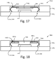
- Figures 17 and 18 illustrate cross-sectional views of various embodiments of systems and methods for EMI shielding that optionally include EMI absorber components avoiding cavity resonances.
- system 1700 includes EMI absorber 1702 within the shielded volume or space of EMI shield 108.
- EMI absorber 1702 can be made from materials such as, for example, ferrites, carbon-loaded polymers, or metal foams that are capable of absorbing electromagnetic energy.
- system 1800 includes both EMI absorbers 1802 and 1804 and TIM layer 700 within the shielded volume of EMI shield 108.
- the EMI absorbers can be layers or components affixed to the EMI shield in any suitable manner including, for example, adhesives, tapes, and/or glues.
- the EMI absorbers can be arranged to completely or partially fill the unoccupied spaces/volume within EMI shield 108.
- Figures 19 and 20 illustrate cross-sectional views of various embodiments of systems and methods for EMI shielding that have a flexible EMI mask component.
- embodiment 1900 includes a PCB carrier plate 1902 that can be made of a conductive and/or insulator material.
- PCB 102 having EMI shield 108 sits within a cavity of the carrier plate 1902.
- a flexible EMI mask 1904 made of a conductive material such as, for example, metal (e.g., aluminum, copper, etc.) is provided.
- Flexible mask 1904 has the ability to bend and to provide a compressive force on to the EMI shield 108 to ensure its contact with the reference voltage of the circuits of PCB 102.
- a thermal interface grease 1906 can be optionally provided to improve the contact between electric circuit 104 and flexible mask 1904 to better thermal transfer from electric circuit 104 to flexible mask 1904.
- Flexible mask 1904 can be secured to carrier plate 1902 by any number of means including, for example, fasteners (screws, clips, clamps, etc.)
- thermal interface grease 1910 can be provided between flexible mask 1904 and carrier plate 1902 to improve the thermal transfer between the components.
- EMI shield 108 includes an opening or aperture in its top portion (e.g., see opening 214 in the embodiments of Figures 2-4 and 7 ). This permits a nearly direct connection between flexible mask 1902 and electric circuit 104 via optional thermal interface grease 1906.
- Embodiment 2000 of Figure 20 is similar to that of Figure 19 except that the connection between flexible mask 1902 and electric circuit 104 is indirect via top portion 200 of EMI shield 108 that does not have an opening or aperture therein.
- thermal interface grease 1906 may be provided on one or both sides of top portion 200 to improve the thermal transfer of heat between electric circuit 104 and flexible mask 1902.
- flexible mask 1902 provides the advantage of tolerance compensation due to various sizes (e.g., height) of electric circuits 104 and associated soldering heights connecting the circuits to the PCB.
- flexible mask 1902 can be provided with geometrically weakened bending areas to control the amount of compressive force being applied to the EMI shield 108 and other components.
- the geometrically weakened areas can, for example, be located near where flexible mask 1902 contacts EMI shield 108.
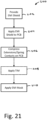
- Method 2100 can begin, for example, in step 2102 where an EMI shield is provided.
- the EMI shield can be, for example, any one of the previously described EMI shields.
- the EMI shield is applied to a PCB and, preferably over at least one electric circuit or component to be shielded.
- one example of such an electric circuit includes MMICs and other circuits/components that emit electromagnetic radio waves or are sensitive to electromagnetic waves.
- the extensions/spring contacts of the EMI shield compress to make connection with a reference layer of the PCB.
- a compressive force is applied to the EMI shield through, for example, application of another component such as an EMI mask, radome cover, etc.
- a TIM layer(s) (and/or thermal interface grease layers) can be optionally applied to the electric circuit directly and/or indirectly via a top portion of the EMI shield or surface of the PCB.
- an EMI mask is applied over the EMI shield to make direct or indirect contact with the EMI shield via, for example, a TIM or thermal interface grease layer(s).
- an electric circuit is provided with a compressive EMI shield that compensates via a spring-like (or flexing or bending or material section torsion) action for PCB irregularities (e.g., warping, bending, etc.) and other irregularities (e.g., integrated circuit height tolerances, soldering heights, etc.)
- PCB irregularities e.g., warping, bending, etc.
- other irregularities e.g., integrated circuit height tolerances, soldering heights, etc.
- the systems and methods disclosed provide electronic EMI shields that can compensate for irregularities associated with PCBs and the circuits thereon.
- the EMI shield includes one or more extensions/spring elements that can compress, flex, bend, or tordate under an applied force to provide a spring-like action for connecting the EMI shield to a reference layer/circuit of a PCB.
- the extensions/spring elements can be, for example, separated by gaps having dimensions that prevent entry/exit of EMI radiation.
- the EMI shield can be economically constructed of, for example, a thin metal material such as aluminum, copper, electrically conductive plastic, plastic components/parts with electrical conductive coating(s), etc. And, the EMI shield can be reliably applied over a range of PCB and electric circuit physical tolerances while still providing effective EMI shielding of the desired components.
- the flexible extensions or spring elements/contacts can have a variety of geometries. This includes for example not only the linear bent sections disclosed, but also sections that gradually and continuously curve to form the same or similar shape/geometry. Accordingly, the described aspects are intended to embrace all such alterations, modifications, and variations that fall within the scope of the appended claims.
Landscapes
- Engineering & Computer Science (AREA)
- Microelectronics & Electronic Packaging (AREA)
- Physics & Mathematics (AREA)
- Electromagnetism (AREA)
- Shielding Devices Or Components To Electric Or Magnetic Fields (AREA)
Priority Applications (2)
| Application Number | Priority Date | Filing Date | Title |
|---|---|---|---|
| EP23168584.3A EP4451818A1 (de) | 2023-04-18 | 2023-04-18 | Systeme und verfahren zur emi-abschirmung |
| US18/308,654 US20240357782A1 (en) | 2023-04-18 | 2023-04-27 | Systems and methods for emi shielding |
Applications Claiming Priority (1)
| Application Number | Priority Date | Filing Date | Title |
|---|---|---|---|
| EP23168584.3A EP4451818A1 (de) | 2023-04-18 | 2023-04-18 | Systeme und verfahren zur emi-abschirmung |
Publications (1)
| Publication Number | Publication Date |
|---|---|
| EP4451818A1 true EP4451818A1 (de) | 2024-10-23 |
Family
ID=86095820
Family Applications (1)
| Application Number | Title | Priority Date | Filing Date |
|---|---|---|---|
| EP23168584.3A Pending EP4451818A1 (de) | 2023-04-18 | 2023-04-18 | Systeme und verfahren zur emi-abschirmung |
Country Status (2)
| Country | Link |
|---|---|
| US (1) | US20240357782A1 (de) |
| EP (1) | EP4451818A1 (de) |
Citations (4)
| Publication number | Priority date | Publication date | Assignee | Title |
|---|---|---|---|---|
| US6985366B2 (en) * | 2002-05-24 | 2006-01-10 | Siemens Aktiengesellschaft | EMC shield and housing for electronic components |
| US20100089619A1 (en) * | 2008-10-13 | 2010-04-15 | Askey Computer Corp. | Circuit board of communication product and manufacturing method thereof |
| US20190004571A1 (en) * | 2017-06-29 | 2019-01-03 | Qualcomm Incorporated | Device comprising compressed thermal interface material (tim) and electromagnetic (emi) shield comprising flexible portion |
| US20220132711A1 (en) * | 2019-07-05 | 2022-04-28 | Denso Corporation | Radar apparatus |
-
2023
- 2023-04-18 EP EP23168584.3A patent/EP4451818A1/de active Pending
- 2023-04-27 US US18/308,654 patent/US20240357782A1/en active Pending
Patent Citations (4)
| Publication number | Priority date | Publication date | Assignee | Title |
|---|---|---|---|---|
| US6985366B2 (en) * | 2002-05-24 | 2006-01-10 | Siemens Aktiengesellschaft | EMC shield and housing for electronic components |
| US20100089619A1 (en) * | 2008-10-13 | 2010-04-15 | Askey Computer Corp. | Circuit board of communication product and manufacturing method thereof |
| US20190004571A1 (en) * | 2017-06-29 | 2019-01-03 | Qualcomm Incorporated | Device comprising compressed thermal interface material (tim) and electromagnetic (emi) shield comprising flexible portion |
| US20220132711A1 (en) * | 2019-07-05 | 2022-04-28 | Denso Corporation | Radar apparatus |
Also Published As
| Publication number | Publication date |
|---|---|
| US20240357782A1 (en) | 2024-10-24 |
Similar Documents
| Publication | Publication Date | Title |
|---|---|---|
| EP1943674B1 (de) | Verfahren und Vorrichtung zur Masseverbindung eines in thermischem Kontakt mit einem elektronischen Bauelement befindlichen Kühlkörpers unter Verwendung von Masseverbindungsfedern bestehend aus mehreren miteinander verbundenen Fingerelementen | |
| US4724443A (en) | Patch antenna with a strip line feed element | |
| US6483024B1 (en) | Panel gasket | |
| US6734045B2 (en) | Lossy RF shield for integrated circuits | |
| CN1336024A (zh) | 天线组件 | |
| US6330167B1 (en) | Electronic assembly with an electromagnetic radiation shielding cap | |
| CN116916543A (zh) | 用于基片集成波导转换的具有超宽频带波导的雷达组件 | |
| US20130322040A1 (en) | Electronic circuit module | |
| JP2001516978A (ja) | シールドされた弾性表面波パッケージ | |
| US7479036B2 (en) | Movable connector bracket for end mounting panel members | |
| KR20180033572A (ko) | 전자 장치 및 그 제조 방법 | |
| US11026355B2 (en) | Housing for receiving electronic devices and electronic system having the same | |
| US20230273295A1 (en) | In-vehicle radar device | |
| KR20190085266A (ko) | 차량용 레이더 장치 | |
| JP2018007107A (ja) | アンテナ装置 | |
| EP4451818A1 (de) | Systeme und verfahren zur emi-abschirmung | |
| US8933346B1 (en) | Miniature surface mount technology electromagnetic interference shielding device | |
| US20220021122A1 (en) | Omnidirectional antenna assembly | |
| EP0951209A2 (de) | HF-Schirmkappe mit niedriger Abmessung für einen strahlenden Stift auf einer Leiterplatte | |
| US20020051344A1 (en) | Covering device for ceramic modules | |
| US10700015B2 (en) | Electronic control unit | |
| US12262483B2 (en) | Electronic device housing | |
| US20240413542A1 (en) | Radio wave absorber for high-frequency communication device | |
| US6316721B1 (en) | Method and a device for shielding electronic components | |
| US6414383B1 (en) | Very low magnetic field integrated circuit |
Legal Events
| Date | Code | Title | Description |
|---|---|---|---|
| PUAI | Public reference made under article 153(3) epc to a published international application that has entered the european phase |
Free format text: ORIGINAL CODE: 0009012 |
|
| STAA | Information on the status of an ep patent application or granted ep patent |
Free format text: STATUS: THE APPLICATION HAS BEEN PUBLISHED |
|
| AK | Designated contracting states |
Kind code of ref document: A1 Designated state(s): AL AT BE BG CH CY CZ DE DK EE ES FI FR GB GR HR HU IE IS IT LI LT LU LV MC ME MK MT NL NO PL PT RO RS SE SI SK SM TR |
|
| P01 | Opt-out of the competence of the unified patent court (upc) registered |
Free format text: CASE NUMBER: APP_60531/2024 Effective date: 20241111 |
|
| STAA | Information on the status of an ep patent application or granted ep patent |
Free format text: STATUS: REQUEST FOR EXAMINATION WAS MADE |
|
| 17P | Request for examination filed |
Effective date: 20250416 |