EP4451533A1 - Dynamische stromgrenzen für gleichstrom-gleichstrom-wandler - Google Patents
Dynamische stromgrenzen für gleichstrom-gleichstrom-wandler Download PDFInfo
- Publication number
- EP4451533A1 EP4451533A1 EP24170865.0A EP24170865A EP4451533A1 EP 4451533 A1 EP4451533 A1 EP 4451533A1 EP 24170865 A EP24170865 A EP 24170865A EP 4451533 A1 EP4451533 A1 EP 4451533A1
- Authority
- EP
- European Patent Office
- Prior art keywords
- current
- circuit
- converter
- voltage
- power management
- Prior art date
- Legal status (The legal status is an assumption and is not a legal conclusion. Google has not performed a legal analysis and makes no representation as to the accuracy of the status listed.)
- Pending
Links
Images


Classifications
-
- H—ELECTRICITY
- H02—GENERATION; CONVERSION OR DISTRIBUTION OF ELECTRIC POWER
- H02M—APPARATUS FOR CONVERSION BETWEEN AC AND AC, BETWEEN AC AND DC, OR BETWEEN DC AND DC, AND FOR USE WITH MAINS OR SIMILAR POWER SUPPLY SYSTEMS; CONVERSION OF DC OR AC INPUT POWER INTO SURGE OUTPUT POWER; CONTROL OR REGULATION THEREOF
- H02M1/00—Details of apparatus for conversion
- H02M1/0003—Details of control, feedback or regulation circuits
- H02M1/0012—Control circuits using digital or numerical techniques
-
- H—ELECTRICITY
- H02—GENERATION; CONVERSION OR DISTRIBUTION OF ELECTRIC POWER
- H02M—APPARATUS FOR CONVERSION BETWEEN AC AND AC, BETWEEN AC AND DC, OR BETWEEN DC AND DC, AND FOR USE WITH MAINS OR SIMILAR POWER SUPPLY SYSTEMS; CONVERSION OF DC OR AC INPUT POWER INTO SURGE OUTPUT POWER; CONTROL OR REGULATION THEREOF
- H02M1/00—Details of apparatus for conversion
- H02M1/0003—Details of control, feedback or regulation circuits
-
- H—ELECTRICITY
- H02—GENERATION; CONVERSION OR DISTRIBUTION OF ELECTRIC POWER
- H02M—APPARATUS FOR CONVERSION BETWEEN AC AND AC, BETWEEN AC AND DC, OR BETWEEN DC AND DC, AND FOR USE WITH MAINS OR SIMILAR POWER SUPPLY SYSTEMS; CONVERSION OF DC OR AC INPUT POWER INTO SURGE OUTPUT POWER; CONTROL OR REGULATION THEREOF
- H02M1/00—Details of apparatus for conversion
- H02M1/0003—Details of control, feedback or regulation circuits
- H02M1/0025—Arrangements for modifying reference values, feedback values or error values in the control loop of a converter
-
- H—ELECTRICITY
- H02—GENERATION; CONVERSION OR DISTRIBUTION OF ELECTRIC POWER
- H02M—APPARATUS FOR CONVERSION BETWEEN AC AND AC, BETWEEN AC AND DC, OR BETWEEN DC AND DC, AND FOR USE WITH MAINS OR SIMILAR POWER SUPPLY SYSTEMS; CONVERSION OF DC OR AC INPUT POWER INTO SURGE OUTPUT POWER; CONTROL OR REGULATION THEREOF
- H02M3/00—Conversion of DC power input into DC power output
- H02M3/02—Conversion of DC power input into DC power output without intermediate conversion into AC
- H02M3/04—Conversion of DC power input into DC power output without intermediate conversion into AC by static converters
- H02M3/10—Conversion of DC power input into DC power output without intermediate conversion into AC by static converters using discharge tubes with control electrode or semiconductor devices with control electrode
- H02M3/145—Conversion of DC power input into DC power output without intermediate conversion into AC by static converters using discharge tubes with control electrode or semiconductor devices with control electrode using devices of a triode or transistor type requiring continuous application of a control signal
- H02M3/155—Conversion of DC power input into DC power output without intermediate conversion into AC by static converters using discharge tubes with control electrode or semiconductor devices with control electrode using devices of a triode or transistor type requiring continuous application of a control signal using semiconductor devices only
-
- H—ELECTRICITY
- H02—GENERATION; CONVERSION OR DISTRIBUTION OF ELECTRIC POWER
- H02M—APPARATUS FOR CONVERSION BETWEEN AC AND AC, BETWEEN AC AND DC, OR BETWEEN DC AND DC, AND FOR USE WITH MAINS OR SIMILAR POWER SUPPLY SYSTEMS; CONVERSION OF DC OR AC INPUT POWER INTO SURGE OUTPUT POWER; CONTROL OR REGULATION THEREOF
- H02M3/00—Conversion of DC power input into DC power output
- H02M3/02—Conversion of DC power input into DC power output without intermediate conversion into AC
- H02M3/04—Conversion of DC power input into DC power output without intermediate conversion into AC by static converters
- H02M3/10—Conversion of DC power input into DC power output without intermediate conversion into AC by static converters using discharge tubes with control electrode or semiconductor devices with control electrode
- H02M3/145—Conversion of DC power input into DC power output without intermediate conversion into AC by static converters using discharge tubes with control electrode or semiconductor devices with control electrode using devices of a triode or transistor type requiring continuous application of a control signal
- H02M3/155—Conversion of DC power input into DC power output without intermediate conversion into AC by static converters using discharge tubes with control electrode or semiconductor devices with control electrode using devices of a triode or transistor type requiring continuous application of a control signal using semiconductor devices only
- H02M3/156—Conversion of DC power input into DC power output without intermediate conversion into AC by static converters using discharge tubes with control electrode or semiconductor devices with control electrode using devices of a triode or transistor type requiring continuous application of a control signal using semiconductor devices only with automatic control of output voltage or current, e.g. switching regulators
-
- H—ELECTRICITY
- H02—GENERATION; CONVERSION OR DISTRIBUTION OF ELECTRIC POWER
- H02M—APPARATUS FOR CONVERSION BETWEEN AC AND AC, BETWEEN AC AND DC, OR BETWEEN DC AND DC, AND FOR USE WITH MAINS OR SIMILAR POWER SUPPLY SYSTEMS; CONVERSION OF DC OR AC INPUT POWER INTO SURGE OUTPUT POWER; CONTROL OR REGULATION THEREOF
- H02M3/00—Conversion of DC power input into DC power output
- H02M3/02—Conversion of DC power input into DC power output without intermediate conversion into AC
- H02M3/04—Conversion of DC power input into DC power output without intermediate conversion into AC by static converters
- H02M3/10—Conversion of DC power input into DC power output without intermediate conversion into AC by static converters using discharge tubes with control electrode or semiconductor devices with control electrode
- H02M3/145—Conversion of DC power input into DC power output without intermediate conversion into AC by static converters using discharge tubes with control electrode or semiconductor devices with control electrode using devices of a triode or transistor type requiring continuous application of a control signal
- H02M3/155—Conversion of DC power input into DC power output without intermediate conversion into AC by static converters using discharge tubes with control electrode or semiconductor devices with control electrode using devices of a triode or transistor type requiring continuous application of a control signal using semiconductor devices only
- H02M3/156—Conversion of DC power input into DC power output without intermediate conversion into AC by static converters using discharge tubes with control electrode or semiconductor devices with control electrode using devices of a triode or transistor type requiring continuous application of a control signal using semiconductor devices only with automatic control of output voltage or current, e.g. switching regulators
- H02M3/157—Conversion of DC power input into DC power output without intermediate conversion into AC by static converters using discharge tubes with control electrode or semiconductor devices with control electrode using devices of a triode or transistor type requiring continuous application of a control signal using semiconductor devices only with automatic control of output voltage or current, e.g. switching regulators with digital control
-
- H—ELECTRICITY
- H03—ELECTRONIC CIRCUITRY
- H03F—AMPLIFIERS
- H03F3/00—Amplifiers with only discharge tubes or only semiconductor devices as amplifying elements
- H03F3/20—Power amplifiers, e.g. Class B amplifiers, Class C amplifiers
- H03F3/24—Power amplifiers, e.g. Class B amplifiers, Class C amplifiers of transmitter output stages
- H03F3/245—Power amplifiers, e.g. Class B amplifiers, Class C amplifiers of transmitter output stages with semiconductor devices only
-
- H—ELECTRICITY
- H02—GENERATION; CONVERSION OR DISTRIBUTION OF ELECTRIC POWER
- H02M—APPARATUS FOR CONVERSION BETWEEN AC AND AC, BETWEEN AC AND DC, OR BETWEEN DC AND DC, AND FOR USE WITH MAINS OR SIMILAR POWER SUPPLY SYSTEMS; CONVERSION OF DC OR AC INPUT POWER INTO SURGE OUTPUT POWER; CONTROL OR REGULATION THEREOF
- H02M3/00—Conversion of DC power input into DC power output
- H02M3/02—Conversion of DC power input into DC power output without intermediate conversion into AC
- H02M3/04—Conversion of DC power input into DC power output without intermediate conversion into AC by static converters
- H02M3/10—Conversion of DC power input into DC power output without intermediate conversion into AC by static converters using discharge tubes with control electrode or semiconductor devices with control electrode
- H02M3/145—Conversion of DC power input into DC power output without intermediate conversion into AC by static converters using discharge tubes with control electrode or semiconductor devices with control electrode using devices of a triode or transistor type requiring continuous application of a control signal
- H02M3/155—Conversion of DC power input into DC power output without intermediate conversion into AC by static converters using discharge tubes with control electrode or semiconductor devices with control electrode using devices of a triode or transistor type requiring continuous application of a control signal using semiconductor devices only
- H02M3/156—Conversion of DC power input into DC power output without intermediate conversion into AC by static converters using discharge tubes with control electrode or semiconductor devices with control electrode using devices of a triode or transistor type requiring continuous application of a control signal using semiconductor devices only with automatic control of output voltage or current, e.g. switching regulators
- H02M3/1566—Conversion of DC power input into DC power output without intermediate conversion into AC by static converters using discharge tubes with control electrode or semiconductor devices with control electrode using devices of a triode or transistor type requiring continuous application of a control signal using semiconductor devices only with automatic control of output voltage or current, e.g. switching regulators with means for compensating against rapid load changes, e.g. with auxiliary current source, with dual mode control or with inductance variation
Definitions
- the technology of the disclosure relates generally to voltage converters such as direct current-to-direct current (DC-DC) converters and providing smooth settling for same.
- DC-DC direct current-to-direct current
- aspects of the present disclosure contemplate a DC-DC converter (e.g., a buck-boost converter) having current and voltage feedback loops.
- Information from the voltage feedback loop may be used to set a reference level for the current feedback loop. This information may be further based on information from a ramp compensation circuit and a current limiting circuit. The accumulated information may then be combined with another output from the ramp compensation circuit to control the DC-DC converter.
- the combination of feedback and elements provides an opportunity to sculpt a voltage output of the DC-DC converter to avoid over and undershooting a target output.
- a power management circuit includes a DC-DC converter, an output node coupled to the DC-DC converter, a current feedback circuit associated with the DC-DC converter, a voltage feedback circuit associated with the DC-DC converter, and a comparator coupled to the current feedback circuit and the voltage feedback circuit, where a voltage output from the voltage feedback circuit is used as a reference for a current output of the current feedback circuit, the comparator further configured to provide a feedback signal to the DC-DC converter.
- a wireless transceiver includes transmit circuitry, including a power amplifier and a power management circuit.
- the power management circuit includes a direct current-to-direct current (DC-DC) converter configured to provide a supply voltage for the power amplifier, an output node coupled to the DC-DC converter, and a current feedback circuit associated with the DC-DC converter.
- the power management circuit also includes a voltage feedback circuit associated with the DC-DC converter and a comparator coupled to the current feedback circuit and the voltage feedback circuit, where a voltage output from the voltage feedback circuit is used as a reference for a current output of the current feedback circuit, the comparator further configured to provide a feedback signal to the DC-DC converter.
- a method of controlling a power management circuit includes detecting a voltage at an output node of a direct current-to-direct current (DC-DC) converter and detecting a current proximate the output node.
- the method also includes modifying a detected voltage with a current limit and a target voltage and using a modified detected voltage as a reference for a current feedback loop.
- DC-DC direct current-to-direct current
- aspects disclosed in the detailed description include systems and methods for dynamic current limits for direct current-to-direct current (DC-DC) converters.
- a DC-DC converter e.g., a buck-boost converter
- Information from the voltage feedback loop may be used to set a reference level for the current feedback loop. This information may be further based on information from a ramp compensation circuit and a current limiting circuit. The accumulated information may then be combined with another output from the ramp compensation circuit to control the DC-DC converter.
- the combination of feedback and elements provides an opportunity to sculpt a voltage output of the DC-DC converter to avoid over and undershooting a target output.
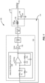
- Figure 1 is a block diagram of a power management circuit 100 that includes a DC-DC converter 102 and an output filter 104 formed from an inductor 106 and a capacitor 108, although other structures for the output filter 104 are possible.
- the output filter 104 couples the DC-DC converter 102 to an output node 110.
- the output node 110 is configured to be coupled to a power amplifier and provide a supply voltage (sometimes referred to as Vout or Vcc) to the power amplifier.
- the output node 110 may also be coupled to a control circuit 112 through a voltage feedback loop 114.
- the control circuit 112 may loosely be considered a stabilization filter 116, a comparator 118, and a pulse width modulation (PWM) circuit 120.
- the stabilization filter 116 provides a signal to the comparator 118.
- the comparator 118 is also coupled to a reference voltage (not shown).
- the PWM circuit 120 provides a pulse to the DC-DC converter 102.
- the pulse width is proportional to a desired supply voltage. For example, wide pulses to the DC-DC converter 102 will cause the DC-DC converter 102 to provide a high voltage and a narrower pulse to provide a lower voltage.
- Other sorts of state machines or control circuits may be present in place of the PWM circuit 120.
- Various other elements such as resistor R, resistor Rz, capacitor Cz, resistor Rint, capacitor C, and capacitor Cint may also be present
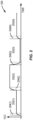
- the power management circuit 100 may have changes in the supply voltage at the output node 110 that provide a steady state voltage for time increments 202(1)-202(N).
- the time increments 202(1)-202(N) may correspond to frames, slots, symbols, or even sub-symbols of data to be transmitted through an antenna (not shown).
- each voltage change between different increments 202(1)-202(N) may be accompanied by a write command to registers in the DC-DC converter 102 that cause the supply voltage to change to the new value.
- additional information on how to manage the transition optimally may also be written to registers in the DC-DC converter 102.
- aspects of the present disclosure provide a dynamic current limiting circuit that allows for fast transitions between voltage levels as well as preventing over and undershooting during settling at the new voltage level.
- the DC-DC converter is controlled by both a voltage feedback loop and a current feedback loop.
- the voltage feedback loop provides a reference current for the current feedback loop.
- the voltage feedback loop also receives information from a ramp compensation circuit that knows the state of the DC-DC converter and the target supply voltage. Based on this information, a dynamic current limit circuit may adjust the voltage feedback loop to a desired reference current. Then, as the supply voltage approaches the desired target level, the current limit may be dynamically adjusted back to a level corresponding to normal operation. Rather than merely turning off the device at high currents, aspects of the present disclosure provide a dynamic current profile that allows for optimal level changes without the risk of damaging the circuitry.
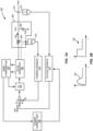
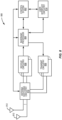
- FIG. 3A provides a block diagram of a power management circuit 300 according to aspects of the present disclosure.
- the power management circuit 300 includes a DC-DC converter 302 and an output filter 304 formed from an inductor 306 (having a current Iout therethrough) and a capacitor 308 (having a capacitance Cout).
- the DC-DC converter 302 may be a buck, a buck-boost, or a boost converter as needed or desired.
- the output filter 304 couples the DC-DC converter 302 to an output node 310.
- a voltage sensor 312 detects the output voltage at the output node 310 and provides this value or information relating to this value to voltage feedback circuit 314.
- a current sensor 316 may detect a current across the inductor 306, some other structure in the output filter 304, or from the DC-DC converter 302 and provide this value or information relating to this value to current feedback circuit 318.
- Values (Iref) from the voltage feedback circuit 314 are compared to values (Ifb) from the current feedback circuit 318 by a summation circuit or comparator 320, where the value from the voltage feedback circuit 314 acts as a reference for the value from the current feedback circuit 318.
- the comparator 320 may inject current forward to be provided to the DC-DC converter 302 through a control circuit 322.
- the difference between the values provides the current to be injected. It should be appreciated that the current feedback performs cycle-to-cycle corrections while the voltage feedback is substantially slower and more readily able to serve as the reference.
- the control circuit 322 also receives input from a ramp compensation circuit 324.
- the ramp compensation circuit 324 knows information on the state of the DC-DC converter 302 relative to the transition being undertaken. This information is used to set a dynamic current limit in a dynamic current limit circuit 326.
- the dynamic current limit circuit 326 sets a dynamic current limit based on the target voltage and the state of the transition. This dynamic current limit is provided to the voltage feedback circuit 314, which adjusts Iref based thereon.
- Figure 3B provides an example of dynamic current limit profiles 330 and 332 comparing current to time.
- the current limit is initially raised so that Iref is initially high, causing current to be injected rapidly at the comparator 320, but then after transition has reached a certain point, the current limit is adjusted back to a level that supports normal operation. Manipulation of this curve may reduce or eliminate the overshoot or undershoot of the transition. Likewise, the curve may be set such that there is no damage to the circuitry while still allowing the transition to occur in an expedient manner.
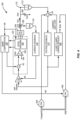
- control circuit 322 is expanded to show a comparator 400 (analogous to the comparator 118) and a state machine 402.
- the state machine 402 may provide state information to the ramp compensation circuit 324 and receive a clock signal (fclk).
- the ramp compensation circuit 324 may also receive the clock signal.
- the control circuit 322 may further include a summation circuit 403 that sums the signal from the ramp compensation circuit 324 with the output of the comparator 320. Additional details are also provided for the voltage feedback loop.
- a target voltage may be supplied, such as from a baseband processor, the DC-DC converter 302, the ramp compensation circuit 324, or other source.
- This target voltage is provided to a first digital-to-analog converter (DAC) 404 and summed with the sensed voltage from voltage sensor 312 by a summation circuit 405. Additionally, some bits (i.e., the most significant bits (MSB)) are provided to a second DAC 406, which provides a current limit (Ilimit) to a voltage clamp 408. The second DAC 406 also receives Iref from the ramp compensation circuit 324. The value of the voltage clamp 408 is also summed with the sensed voltage from the voltage sensor 312 at the summation circuit 405. The voltage clamp 408 also receives a feedback signal from the voltage feedback circuit 314. This structure provides a current limit loop, where the target voltage and Iref adjust the current limit dynamically.
- DAC digital-to-analog converter
- Figure 5 provides other additional details about the power management circuit 300 and, in particular, about the current limit loop 500 as well as explicitly showing voltage-to-current converters 502, 504 that provide currents to the summation circuit or comparator 320 (since currents are easier to sum than voltages).
- the control circuit 322 may include a voltage-to-current converter 506 so that the comparator 400 may compare voltages more readily.
- the threshold for the current limit (Ilimit) may be generated as a voltage level (Vlimit) that goes into a reference input of a transconductance circuit 508.
- the Vlimit can be generated by injecting a current from a DAC 510 into a resistance 512.
- the DAC 510 allows adjustment to a static component of the current limit.
- the transconductance circuit 508 is used to close a feedback loop around the voltage feedback circuit 314.
- a dominant pole circuit 514 may be added to the feedback limiting local loop to provide stable operation of the voltage feedback circuit 314.
- the process 700 begins by detecting a voltage at the output node 310 (block 702) and detecting a current at or near the output node 310 (block 704).
- the detected voltage is modified by a current limit and a target voltage (block 706).
- the modified voltage is used as a reference for a current feedback loop (block 708), where the detected current is compared to the modified voltage to get a correction value for a DC-DC converter 302. It should be appreciated the current limit is based on the ramp compensation circuit 324 and the target voltage.
- control system 802 can include at least a microprocessor(s), an embedded memory circuit(s), and a communication bus interface(s).
- the receive circuitry 808 receives radio frequency signals via the antennas 812 and through the antenna switching circuitry 810 from one or more base stations.
- a low noise amplifier and a filter of the receive circuitry 808 cooperate to amplify and remove broadband interference from the received signal for processing.
- Downconversion and digitization circuitry (not shown) will then downconvert the filtered, received signal to an intermediate or baseband frequency signal, which is then digitized into one or more digital streams using an analog-to-digital converter(s) (ADC).
- ADC analog-to-digital converter
- the baseband processor 804 processes the digitized received signal to extract the information or data bits conveyed in the received signal. This processing typically comprises demodulation, decoding, and error correction operations.
- the baseband processor 804 is generally implemented in one or more digital signal processors (DSPs) and ASICs.
- the baseband processor 804 receives digitized data, which may represent voice, data, or control information, from the control system 802 that it encodes for transmission.
- the encoded data is output to the transmit circuitry 806, where a digital-to-analog converter(s) (DAC) converts the digitally encoded data into an analog signal, and a modulator modulates the analog signal onto a carrier signal that is at a desired transmit frequency or frequencies.
- a power amplifier will amplify the modulated carrier signal to a level appropriate for transmission and deliver the modulated carrier signal to the antennas 812 through the antenna switching circuitry 810 to the antennas 812.
- power management circuits may work with the power amplifier to assist in providing efficient operation of the power amplifier.
- the multiple antennas 812 and the replicated transmit and receive circuitries 806, 808 may provide spatial diversity. Modulation and processing details will be understood by those skilled in the art.
- a computer readable medium may include non-transitory type media such as physical storage media including storage discs and solid state devices.
- a computer readable medium may also or alternatively include transient media such as carrier signals and transmission media.
- a computer-readable storage medium is defined herein as a non-transitory memory device.
- a memory device includes memory space within a single physical storage device or memory space spread across multiple physical storage devices.
- a DC-DC converter e.g., a buck-boost converter having dual current and voltage feedback loops.
- Information from the voltage feedback loop may be used to set a reference level for the current feedback loop. This information may be further based on information from a ramp compensation circuit and a current limiting circuit. The accumulated information may then be combined with another output from the ramp compensation circuit to control the DC-DC converter.
- the combination of feedback and elements provides an opportunity to sculpt a voltage output of the DC-DC converter to avoid over and undershooting a target output.
Landscapes
- Engineering & Computer Science (AREA)
- Power Engineering (AREA)
- Dc-Dc Converters (AREA)
Applications Claiming Priority (2)
| Application Number | Priority Date | Filing Date | Title |
|---|---|---|---|
| US202363460975P | 2023-04-21 | 2023-04-21 | |
| US18/627,584 US20240356424A1 (en) | 2023-04-21 | 2024-04-05 | Dynamic current limits for direct current-to-direct current (dc-dc) converters |
Publications (1)
| Publication Number | Publication Date |
|---|---|
| EP4451533A1 true EP4451533A1 (de) | 2024-10-23 |
Family
ID=90789670
Family Applications (1)
| Application Number | Title | Priority Date | Filing Date |
|---|---|---|---|
| EP24170865.0A Pending EP4451533A1 (de) | 2023-04-21 | 2024-04-17 | Dynamische stromgrenzen für gleichstrom-gleichstrom-wandler |
Country Status (2)
| Country | Link |
|---|---|
| US (1) | US20240356424A1 (de) |
| EP (1) | EP4451533A1 (de) |
Citations (3)
| Publication number | Priority date | Publication date | Assignee | Title |
|---|---|---|---|---|
| US8773097B2 (en) * | 2011-01-06 | 2014-07-08 | Texas Instruments Incorporated | Digital peak current mode control for switch-mode power converters |
| US9379621B1 (en) * | 2015-01-28 | 2016-06-28 | Microchip Technology Incorporated | Digital slope compensation for peak current controlled converters |
| US11183928B2 (en) * | 2015-01-12 | 2021-11-23 | Hua Cao | Switching regulator and control method thereof |
Family Cites Families (6)
| Publication number | Priority date | Publication date | Assignee | Title |
|---|---|---|---|---|
| US20130147277A1 (en) * | 2011-12-08 | 2013-06-13 | O2Micro Inc. | Power management system |
| US9756572B2 (en) * | 2014-12-04 | 2017-09-05 | Texas Instruments Incorporated | Reduction of power consumption in a half-duplex transceiver |
| DE102016217857A1 (de) * | 2016-09-19 | 2018-03-22 | Dialog Semiconductor (Uk) Limited | Spitzenstromservo |
| US12348136B2 (en) * | 2022-01-11 | 2025-07-01 | Mediatek Inc. | Apparatus and method for improving adaptive voltage positioning performance of voltage regulator by sensing output capacitor current |
| US20240339918A1 (en) * | 2023-04-05 | 2024-10-10 | Qorvo Us, Inc. | Systems and methods for improving efficiency in a power management circuit |
| US20250266753A1 (en) * | 2024-02-19 | 2025-08-21 | Qorvo Us, Inc. | Ripple reduction for direct current-to-direct current (dc-dc) converters |
-
2024
- 2024-04-05 US US18/627,584 patent/US20240356424A1/en active Pending
- 2024-04-17 EP EP24170865.0A patent/EP4451533A1/de active Pending
Patent Citations (3)
| Publication number | Priority date | Publication date | Assignee | Title |
|---|---|---|---|---|
| US8773097B2 (en) * | 2011-01-06 | 2014-07-08 | Texas Instruments Incorporated | Digital peak current mode control for switch-mode power converters |
| US11183928B2 (en) * | 2015-01-12 | 2021-11-23 | Hua Cao | Switching regulator and control method thereof |
| US9379621B1 (en) * | 2015-01-28 | 2016-06-28 | Microchip Technology Incorporated | Digital slope compensation for peak current controlled converters |
Also Published As
| Publication number | Publication date |
|---|---|
| US20240356424A1 (en) | 2024-10-24 |
Similar Documents
| Publication | Publication Date | Title |
|---|---|---|
| US9442140B2 (en) | Average current mode control of multi-phase switching power converters | |
| KR102704900B1 (ko) | 동적으로 출력 전압을 변경하는 스위칭 레귤레이터 및 이를 포함하는 전원 회로 | |
| US7948720B2 (en) | Voltage regulator with transient recovery circuit | |
| EP3198718B1 (de) | Digitales pwm-hüllkurvennachführungssystem mit offener schleife mit dynamischer verstärkung | |
| US11005368B2 (en) | Hysteretic window adjustment of tri-level switching regulator | |
| US7821238B1 (en) | Feedback loop compensation for buck/boost switching converter | |
| US20160164551A1 (en) | Envelope tracking with reduced circuit area and power consumption | |
| EP2965413B1 (de) | Übertragungsfunktionserzeugung auf basis von pulsweitenmodulationsinformationen | |
| US9480017B2 (en) | Dynamic power management control | |
| WO2013165401A1 (en) | Voltage regulator with adaptive control | |
| CN105009434B (zh) | 开关功率转换器 | |
| US11342842B2 (en) | Pulse frequency modulation and frequency avoidance method and implementation for switching regulators | |
| US20200266707A1 (en) | Buck converter | |
| KR20160043076A (ko) | 디지털 마이크로폰용 슬루 레이트 제어 장치 | |
| KR20140081708A (ko) | 프로그래밍 가능한 전력 변환기를 제어하는 방법 및 장치 | |
| EP4451533A1 (de) | Dynamische stromgrenzen für gleichstrom-gleichstrom-wandler | |
| US20250266753A1 (en) | Ripple reduction for direct current-to-direct current (dc-dc) converters | |
| US8896383B2 (en) | Enhanced pulse frequency modulation (PFM) control mode for switching regulators | |
| EP4451532A1 (de) | Systeme und verfahren zur verbesserung der effizienz in einer leistungsverwaltungsschaltung | |
| CN118826456A (zh) | 直流电-直流电(dc-dc)转换器的动态电流限制 | |
| EP4443728A1 (de) | Gleichstrom-gleichstrom-wandler mit programmierbarer kompensation | |
| CA2658532A1 (en) | Methods and apparatuses for providing input voltages to power amplifiers | |
| US20070200542A1 (en) | Voltage regulating power supply for noise sensitive circuits | |
| WO2025024053A1 (en) | Systems and method for smooth transitions in a buck-boost direct current-to-direct current (dc-dc) converter | |
| CN121620847A (zh) | 功率管理电路中的无冲突电流分配 |
Legal Events
| Date | Code | Title | Description |
|---|---|---|---|
| PUAI | Public reference made under article 153(3) epc to a published international application that has entered the european phase |
Free format text: ORIGINAL CODE: 0009012 |
|
| STAA | Information on the status of an ep patent application or granted ep patent |
Free format text: STATUS: THE APPLICATION HAS BEEN PUBLISHED |
|
| AK | Designated contracting states |
Kind code of ref document: A1 Designated state(s): AL AT BE BG CH CY CZ DE DK EE ES FI FR GB GR HR HU IE IS IT LI LT LU LV MC ME MK MT NL NO PL PT RO RS SE SI SK SM TR |
|
| STAA | Information on the status of an ep patent application or granted ep patent |
Free format text: STATUS: REQUEST FOR EXAMINATION WAS MADE |
|
| 17P | Request for examination filed |
Effective date: 20250416 |