EP4451118A1 - Programmladeverfahren und -vorrichtung sowie computerlesbares medium und elektronische vorrichtung - Google Patents
Programmladeverfahren und -vorrichtung sowie computerlesbares medium und elektronische vorrichtung Download PDFInfo
- Publication number
- EP4451118A1 EP4451118A1 EP23742708.3A EP23742708A EP4451118A1 EP 4451118 A1 EP4451118 A1 EP 4451118A1 EP 23742708 A EP23742708 A EP 23742708A EP 4451118 A1 EP4451118 A1 EP 4451118A1
- Authority
- EP
- European Patent Office
- Prior art keywords
- speed
- spi
- fsbl
- flash memory
- program loading
- Prior art date
- Legal status (The legal status is an assumption and is not a legal conclusion. Google has not performed a legal analysis and makes no representation as to the accuracy of the status listed.)
- Pending
Links
Images


Classifications
-
- G—PHYSICS
- G06—COMPUTING OR CALCULATING; COUNTING
- G06F—ELECTRIC DIGITAL DATA PROCESSING
- G06F9/00—Arrangements for program control, e.g. control units
- G06F9/06—Arrangements for program control, e.g. control units using stored programs, i.e. using an internal store of processing equipment to receive or retain programs
- G06F9/44—Arrangements for executing specific programs
- G06F9/445—Program loading or initiating
-
- G—PHYSICS
- G06—COMPUTING OR CALCULATING; COUNTING
- G06F—ELECTRIC DIGITAL DATA PROCESSING
- G06F9/00—Arrangements for program control, e.g. control units
- G06F9/06—Arrangements for program control, e.g. control units using stored programs, i.e. using an internal store of processing equipment to receive or retain programs
- G06F9/44—Arrangements for executing specific programs
- G06F9/445—Program loading or initiating
- G06F9/44505—Configuring for program initiating, e.g. using registry, configuration files
-
- G—PHYSICS
- G06—COMPUTING OR CALCULATING; COUNTING
- G06F—ELECTRIC DIGITAL DATA PROCESSING
- G06F9/00—Arrangements for program control, e.g. control units
- G06F9/06—Arrangements for program control, e.g. control units using stored programs, i.e. using an internal store of processing equipment to receive or retain programs
- G06F9/44—Arrangements for executing specific programs
- G06F9/4401—Bootstrapping
-
- G—PHYSICS
- G06—COMPUTING OR CALCULATING; COUNTING
- G06F—ELECTRIC DIGITAL DATA PROCESSING
- G06F1/00—Details not covered by groups G06F3/00 - G06F13/00 and G06F21/00
- G06F1/04—Generating or distributing clock signals or signals derived directly therefrom
- G06F1/08—Clock generators with changeable or programmable clock frequency
-
- G—PHYSICS
- G06—COMPUTING OR CALCULATING; COUNTING
- G06F—ELECTRIC DIGITAL DATA PROCESSING
- G06F21/00—Security arrangements for protecting computers, components thereof, programs or data against unauthorised activity
- G06F21/50—Monitoring users, programs or devices to maintain the integrity of platforms, e.g. of processors, firmware or operating systems
- G06F21/51—Monitoring users, programs or devices to maintain the integrity of platforms, e.g. of processors, firmware or operating systems at application loading time, e.g. accepting, rejecting, starting or inhibiting executable software based on integrity or source reliability
-
- G—PHYSICS
- G06—COMPUTING OR CALCULATING; COUNTING
- G06F—ELECTRIC DIGITAL DATA PROCESSING
- G06F21/00—Security arrangements for protecting computers, components thereof, programs or data against unauthorised activity
- G06F21/50—Monitoring users, programs or devices to maintain the integrity of platforms, e.g. of processors, firmware or operating systems
- G06F21/57—Certifying or maintaining trusted computer platforms, e.g. secure boots or power-downs, version controls, system software checks, secure updates or assessing vulnerabilities
- G06F21/575—Secure boot
-
- G—PHYSICS
- G06—COMPUTING OR CALCULATING; COUNTING
- G06F—ELECTRIC DIGITAL DATA PROCESSING
- G06F9/00—Arrangements for program control, e.g. control units
- G06F9/06—Arrangements for program control, e.g. control units using stored programs, i.e. using an internal store of processing equipment to receive or retain programs
- G06F9/44—Arrangements for executing specific programs
- G06F9/445—Program loading or initiating
- G06F9/44568—Immediately runnable code
- G06F9/44578—Preparing or optimising for loading
-
- Y—GENERAL TAGGING OF NEW TECHNOLOGICAL DEVELOPMENTS; GENERAL TAGGING OF CROSS-SECTIONAL TECHNOLOGIES SPANNING OVER SEVERAL SECTIONS OF THE IPC; TECHNICAL SUBJECTS COVERED BY FORMER USPC CROSS-REFERENCE ART COLLECTIONS [XRACs] AND DIGESTS
- Y02—TECHNOLOGIES OR APPLICATIONS FOR MITIGATION OR ADAPTATION AGAINST CLIMATE CHANGE
- Y02D—CLIMATE CHANGE MITIGATION TECHNOLOGIES IN INFORMATION AND COMMUNICATION TECHNOLOGIES [ICT], I.E. INFORMATION AND COMMUNICATION TECHNOLOGIES AIMING AT THE REDUCTION OF THEIR OWN ENERGY USE
- Y02D10/00—Energy efficient computing, e.g. low power processors, power management or thermal management
Definitions
- the present disclosure relates to hardware program loading, and in particular, to a method, apparatus, computer-readable medium and electronic device for program loading.
- Bootrom or Boot ROM is a small piece of mask ROM or write-protected flash memory embedded in a CPU chip, which may not be flexibly modified. If a first-stage boot loader (FSBL) of an embedded system (such as various accelerator cards on a server) is in a serial peripheral interface flash (SPI flash memory), the Bootrom needs to load the FSBL into Static Random-Access Memory (SRAM) after the CPU is powered on, verify and execute FSBL. Due to security requirements, even the eXecute In Place (XIP) way needs to read the entire FSBL and verify it before jumping to execution.
- FSBL first-stage boot loader
- SRAM Static Random-Access Memory
- the clock rate of the SPI controller in the Bootrom is relatively low (usually about 10MHz), resulting in a long time to load FSBL, which may not be applied to occasions that are sensitive to startup time.
- the present disclosure provides a method for program, the method being implemented at an electronic device.
- the method includes: loading the bin file at a program loading speed that is a first speed; the bin file comprising a configuration parameter for adjusting the program loading speed; adjusting the program loading speed to a second speed based on the configuration parameter in the bin file; the second speed being faster than the first speed; and loading a first-stage bootloader, FSBL, at the program loading speed which is adjusted to the second speed.
- the present disclosure provides an apparatus program loading, the apparatus being implemented at an electronic device.
- the apparatus includes: a loading module configured to load the bin file at a program loading speed that is a first speed; the bin file comprising a configuration parameter for adjusting the program loading speed; a processing module configured to adjust the program loading speed to a second speed based on the configuration parameter in the bin file; the second speed being faster than the first speed; and the loading module being further configured to load a first-stage bootloader, FSBL, at the program loading speed which is adjusted to the second speed.
- FSBL first-stage bootloader
- the present disclosure provides a computer-readable medium having a computer program stored thereon that, when executed by a processing device, implements the steps of the aforementioned method.
- the present disclosure provides an electronic device, comprising: a storage device having a computer program stored thereon; and a processing device configured to execute the computer program in the storage device to implement the steps of the aforementioned method.
- the bin file in the flash memory is loaded at the program loading speed that is the first speed, and the program loading speed is adjusted to the second speed based on the configuration parameter in the bin file.
- the second speed is faster than the first speed, and then the FBSL is loaded at the second speed.
- 100-electronic device 10-Boot ROM; 20-SPI flash memory; 20- apparatus for program loading; 201-loading module; 203-processing module; 600-computer device; 601-processing device; 602-ROM; 603-RAM; 604-bus; 605-I/O interface; 606-input device; 607-output device; 608-storage device; 609-communication device.
- Boot ROM (Bootrom) is the code solidified in the internal ROM of a CPU.
- the Bootrom contains the first code executed by the processor when it is powered on or reset. Depending on the configuration of certain strap pins or internal fuses, it may decide where to load the next part of the code to be executed as well as verify that the code to be executed is correct or valid. Sometimes, the Bootrom may also contain additional functions that may be used by user code during or after boot. For example, for iPhone boot ROM, the code embedded in the mask ROM cannot be modified, the ROM loads the next-level bootloader from flash memory (flash) or USB and uses the built-in RSA algorithm to verify the signature of the bootloader, and the ROM provides the accelerated decryption function for the next-level bootloader.
- SPI flash is a flash storage device that operates through the serial peripheral interface (SPI). Flash is usually divided into two types according to different internal storage structures: Nor flash and Nand flash. Here, the SPI flash belongs to Nor flash. SPI flash reads and writes slowly, and the number of reads and writes is also limited. It is generally used for storage that does not change frequently.
- the interface of early stage Nor flash is in the form of parallel, that is, the data lines and address lines are connected side by side to the pins of the integrated circuit (IC). But later, people in the industry discover that Nor flash with different capacities is not compatible in hardware because the number of data lines and address lines is different, and the package is relatively large, occupying a larger area of a printed circuit board (PCB), and thus it is gradually replaced by SPI Nor flash later.
- PCB printed circuit board
- the XIP way means that the application may be run directly in flash without having to read the code into the system Random Access Memory (RAM).
- Execution in flash means that Nor flash does not need to be initialized and the code may be executed directly in flash. However, often only part of the code is executed, such as initializing RAM.
- the Bootrom needs to load the FSBL to SRAM after the CPU is powered on.
- the signature of the FSBL needs to be verified and then the FSBL is executed. Even the XIP way requires reading the entire FSBL and verifying the signature before executing the FSBL.
- a SPI controller that support high-speed clock (CLK) (high-speed here usually refers to a clock frequency greater than 25MHz, that is, CLK > 25MHz), it usually has a port physical layer (PHY).
- the PHY register needs to be adapted according to the wiring of the circuit board, flash parameters, etc. to work.
- the Bootrom is solidified inside the CPU chip and cannot flexibly customize the values of these PHY registers. Even though some high-speed SPI controllers may modify the value of the PHY register through jumpers, this jumper way may not cover all related PHY registers. Therefore, when the Bootrom reads the FSBL, the clock rate of the SPI controller cannot be set too high, such as usually not higher than 25MHz.
- SPI is divided into three modes which are Single SPI (standard SPI, transmitting 1 bit in one clock), Dual SPI (double SPI, transmitting 2 bits in one clock) and Quad SPI (quadruple SPI, transmitting 4 bits in one clock), corresponding to 3-wire, 4-wire and 6-wire respectively. Under the same clock, the more the number of wires, the higher the data transmission rate. Most SPI flash support QSPI (Quad SPI), but the CPU needs to read the serial flash discoverable parameter (flash SFDP) to determine how to enable QSPI. However, these logics are cumbersome and complicated and not suitable for putting into the Bootrom.
- the clock rate of the SPI controller in the Bootrom is relatively conservative (about 10MHz), and the QSPI mode of SPI is rarely turned on, resulting in too long loading time of the FSBL.
- PCIe peripheral component interconnect express
- the present disclosure proposes a method for program loading of the Bootrom that may be applied to embedded systems. This method shortens the time for the Bootrom to load FSBL from SPI flash. The following will provide a detailed explanation of this method.
- FIG. 1 shows a schematic structural diagram of an electronic device provided by an example embodiment of the present disclosure.
- the electronic device 100 includes a boot ROM (Bootrom) 10 and a SPI flash memory (SPI flash) 20.
- the SPI flash memory 20 may be a SPI Nor flash.
- a bin file may be stored in the SPI flash memory 20.
- the Bootrom establishes a communication connection with the SPI flash memory 20. Firstly, the Bootrom verifies the security of the SPI flash memory 20, and after the SPI flash memory 20 passes the security verification, the Bootrom reads the relevant code in the SPI flash memory 20 and executes it, to obtain relevant parameters to adapt the PHY register, or adjust the clock rate of the SPI controller. Then, the FSBL is read from the SPI flash memory 20 and security verification perform. After the FSBL passes the security verification, the Bootrom executes the FSBL.
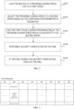
- FIG. 2 is a flowchart of a method for program loading provided by an example embodiment of the present disclosure.
- the method may include the following steps.
- the bin file is loaded at a program loading speed that is a first speed.
- the clock rate of the SPI controller in the Bootrom is relatively low, which is about 10MHz. Therefore, the first speed in this step is a reasonable value in this field. This value may be obtained based on human experience or other feasible ways.
- the first speed may be but not limited to the clock rate value of the SPI controller which is 10MHz.
- the bin file is stored in the SPI flash.
- the bin file contains a configuration parameter for adjusting the program loading speed.
- the configuration parameter includes at least one of the following: a PHY register configuration parameter, a flash memory adaptation parameter, and a SPI clock rate parameter.
- the PHY register configuration parameter is used to adjust the PHY register configuration of the board-level wiring of the embedded system, specifically to adjust the phase relationship between the SPI signals, so that the SPI may work normally.
- the SPI clock rate parameter is used to adjust the clock rate of the SPI controller, and the flash memory adaptation parameter is used to enable the QSPI mode of the SPI.
- the program loading speed is adjusted to a second speed based on the configuration parameter in the bin file.
- the PHY register configuration of the board-level wiring of the embedded system is adjusted based on the PHY register configuration parameter in the bin file, specifically to adjust the phase relationship between the SPI signals, so that the SPI may work normally.
- the value of the second speed is greater than the first speed.
- the second speed is a reasonable value in this field. This value may be obtained based on human experience or other feasible ways.
- the second speed may be but not limited to the clock rate of the SPI controller which is 50MHz.
- the way of adjusting the program loading speed to the second speed based on the configuration parameter in the bin file may be enabling a QSPI mode of a SPI based on the flash memory adaptation parameter, to cause the program loading speed to reach the second speed.
- SPI may be divided into the above three modes: Single SPI, Dual SPI and Quad SPI, which correspond to 3-wire, 4-wire and 6-wire respectively. Under the same clock, the more the number of wires, the higher the data transmission rate. Flashes manufactured by different companies correspond to different adjustment ways. The specific adjustment ways may be obtained based on the flash manual given by the company, which is not limited in this disclosure. For example, the flash of a certain company is taken as an example to illustrate, as shown in FIG.
- Bit0-bit7 are all registers, where Quad Enable (QE) is usually controlled by the bit6 register, that is, the QSPI mode is controlled by the bit6 register.
- QE Quad Enable
- the way of adjusting the program loading speed to the second speed based on the configuration parameter in the bin file may further be adjusting a clock rate of the SPI based on the SPI clock rate parameter in the bin file, to cause the program loading speed to reach the second speed.
- the clock rate of the SPI controller may be adjusted to 50MHz.
- the way of adjusting the program loading speed to the second speed based on the configuration parameter in the bin file may further be enabling the QSPI mode of the SPI based on the flash memory adaptation parameter in the bin file and adjusting the clock rate of the SPI based on the SPI clock rate parameter in the bin file, to cause the program loading speed to reach the second speed.
- the clock rate of the controller is adjusted to allow the program loading speed to reach the second speed.
- the clock rate of the SPI controller may be adjusted to 50MHz.
- the first stage loading program (FSBL) is loaded at the program loading speed which is adjusted to the second speed.
- the Bootrom reads FSBL from SPI flash at the second speed program loading speed. Normally, the second speed can be adjusted to 4-5 times the first speed, thereby achieving the purpose of loading FSBL at a high speed.
- the configuration parameter in the bin file is executed to adjust the speed of the Bootrom loading the FSBL from the flash memory, which shortens the time for the Bootrom to load the FSBL and thus embedded systems are enabled to be compatible with various flash memories while also being applicable in occasions sensitive to startup time.
- Products that are forced to use SD/MMC related registers may use SPI flash instead due to Bootrom startup speed limitations, thereby reducing hardware costs.
- the above method may further include the following steps.
- step S104 security verification is performed on the FSBL.
- the security verification on the FSBL using the MD5 algorithm is used as an example for explanation.
- the FSBL and a first encrypted signature of the FSBL are packaged together and stored in the SPI flash.
- the first encrypted signature is obtained by encrypting the signature of FSBL with a private key.
- the FSBL and the first encrypted signature of the FSBL are obtained from the FSBL loaded at step S103, and then the first encrypted signature is decrypted by a public key pre-stored in Bootrom corresponding to the private key, to obtain the decrypted first signature.
- the signature of FSBL is calculated to obtain the second signature of FSBL and the first signature is compared with the second signature. When the first signature is the same as the second signature, it is determined that the FSBL passes the security verification.
- step S105 if the FSBL passes the security verification, the FSBL is executed.
- the specific implementation of the method for program loading provided by the present disclosure may be to add a plug-in in the Bootrom.
- the plug-in is not only limited to high-speed loading of the FSBL, but may also achieve other purposes by adjusting the code in the plug-in. For example, some flashes may only access the first 16M address space without special configuration. After configuring the corresponding access address space plug-in, it may be expanded to the 4G address space.
- the method for program loading includes: loading the bin file in the SPI flash at a program loading speed that is a first speed, adjusting the program loading speed to a second speed based on a configuration parameter in the bin file, the second speed being faster than the first speed and loading a FSBL at the program loading speed that is a second speed.
- the speed of the Bootrom loading the FSBL from SPI flash is adjusted, which shortens the time for the Bootrom to load FSBL, and thus embedded systems are enabled to be compatible with various flash memories while also being applicable in occasions sensitive to startup time.
- FIG. 4 is a block diagram of an apparatus program loading provided by an example embodiment of the present disclosure.
- the apparatus 20 includes a loading module 201 and a processing module 203.
- the loading module 201 is configured to load the bin file at a program loading speed that is a first speed; the bin file comprising a configuration parameter for adjusting the program loading speed.
- the processing module 203 is configured to adjust the program loading speed to a second speed based on the configuration parameter in the bin file; the second speed being faster than the first speed.
- the loading module 201 is further configured to load a first-stage bootloader, FSBL, at the program loading speed which is adjusted to the second speed.
- the configuration parameter comprises at least one of the following: a port physical layer, PHY, register configuration parameter, a flash memory adaptation parameter, or a serial peripheral interface, SPI, clock rate parameter.
- processing module 203 is configured to:
- processing module 203 is further configured to:
- processing module 203 is configured to:
- FIG. 5 shows a structural schematic diagram of an electronic device 600 adapted to implement the embodiments of the present disclosure.
- the terminal device may include, but not limited to, mobile terminals such as a mobile phone, a laptop computer, a digital broadcast receiver, a Personal Digital Assistant (PDA), a tablet computer or PAD, a Portable Multimedia Player (PMP), and an in-vehicle terminal (e.g., an in-vehicle navigation terminal), and fixed terminals such as a digital TV and a desktop computer.
- PDA Personal Digital Assistant
- PMP Portable Multimedia Player
- in-vehicle terminal e.g., an in-vehicle navigation terminal
- fixed terminals such as a digital TV and a desktop computer.
- the electronic device illustrated in FIG. 5 is merely an example and should not be construed as limiting the function and scope of use of the embodiments of the present disclosure.
- the electronic device 600 may include a processing device 601 (e.g., a central processor, a graphics processor, etc.), which may perform various appropriate actions and processing in accordance with programs stored in a read only memory (ROM) 602 or loaded from a storage device 608 into a random access memory (RAM) 603. Various programs and data required for operation of the electronic device 600 may also be stored in the RAM 603.
- the processing device 601, the ROM 602, and the RAM 603 are connected to each other through a bus 604.
- An input/output (I/O) interface 605 is also connected to bus 604.
- the following devices may be connected to the I/O interface 605: an input device 606 including, for example, a touch screen, a touch pad, a keyboard, a mouse, a camera, a microphone, an accelerometer, a gyroscope, etc.; an output device 607 including, for example, a liquid crystal display (LCD), a speaker, a vibrator, and the like; a storage device 608 including, for example, magnetic tape, hard disk, etc.; and a communication device 609.
- the communication device 609 may allow the electronic device 600 to perform wireless or wired communication with other devices for data exchange.
- FIG. 5 illustrates the electronic device 600 having various devices, it should be understood that it is not necessary to implement or provide all the illustrated devices. Alternatively, more or fewer devices may be implemented or provided.
- the above computer-readable medium in the present disclosure may be a computer-readable signal medium or a computer-readable storage medium or any combination thereof.
- the computer-readable storage medium may be, but not limited to, for example, an electrical, magnetic, optical, electromagnetic, infrared, or semiconductor system, apparatus, or device, or any combination thereof.
- the computer-readable storage medium may include, but not limited to: an electrical connection having one or more wires, a portable computer disk, a hard disk, a random access memory (RAM), a read only memory (ROM), an erasable programmable read only memory (EPROM) or a flash memory, an optical fiber, a compact disc read-only memory (CD-ROM), an optical storage device, a magnetic storage device, or any suitable combination thereof.
- the computer-readable storage medium may be any tangible medium including or storing programs, which may be used by or used with an instruction execution system, apparatus, or device.
- the computer-readable signal medium may include a data signal propagated in a baseband or as a part of a carrier that carries computer-readable program codes. Such propagated data signal may be in various forms, including but not limited to an electromagnetic signal, an optical signal, or any suitable combination thereof.
- the computer-readable signal medium may be any computer-readable medium other than the computer-readable storage medium, which may transmit, propagate, or transfer programs used by or used with an instruction execution system, apparatus or device.
- the program codes contained on the computer-readable medium may be transmitted via any appropriate medium, including but not limited to electric cable, optical cable, Radio Frequency (RF), or any suitable combination thereof.
- RF Radio Frequency
- the above-mentioned computer readable medium may be contained in the above-mentioned electronic device or may be standalone without being assembled into the electronic device.
- the above-mentioned computer-readable medium carries one or more programs.
- the one or more programs When the one or more programs are executed by the electronic device, cause the electronic device to: loading the bin file at a program loading speed that is a first speed; the bin file comprising a configuration parameter for adjusting the program loading speed; adjusting the program loading speed to a second speed based on the configuration parameter in the bin file; the second speed being faster than the first speed; and loading a first-stage bootloader, FSBL, at the program loading speed which is adjusted to the second speed.
- FSBL first-stage bootloader
- the computer program codes for implementing the operations of the present disclosure may be written in one or more programming languages or any combination thereof.
- the programming languages may include object-oriented programming languages, such as Java, Smalltalk, or C++, as well as conventional procedure-oriented programming languages, such as "C" language or similar programming languages.
- the program codes may be executed completely on a user computer, partly on the user computer, as a standalone software package, partly on the user computer and partly on a remote computer, or completely on the remote computer or server.
- the remote computer may be connected to the user computer through any types of networks, including a Local Area Network (LAN) or a Wide Area Network (WAN), or to an external computer (e.g., over the Internet by using an Internet service provider).
- LAN Local Area Network
- WAN Wide Area Network
- each block in the flowcharts or block diagrams may represent a module, a program segment, or a part of codes.
- the module, program segment, or part of codes may contain one or more executable instructions for implementing a specified logical function.
- the functions showed in blocks may occur in an order other than the order illustrated in the drawings. For example, two blocks illustrated in succession may actually be executed substantially in parallel with each other, or sometimes even in a reverse order, depending on functions involved.
- each block in the block diagrams and/or flowcharts, or any combination of the blocks in the block diagrams and/or flowcharts may be implemented using a dedicated hardware-based system configured to perform specified functions or operations or may be implemented using a combination of dedicated hardware and computer instructions.
- the modules involved in the embodiments described in this disclosure may be implemented in software or hardware.
- the name of the module does not constitute a limitation on the module itself under certain circumstances.
- exemplary types of suitable hardware logic components include a field programmable gate array (FPGA), an application specific integrated circuit (ASIC), an application specific standard product (ASSP), a system on chip (SOC), a complex programmable logic device (CPLD), and the like.
- FPGA field programmable gate array
- ASIC application specific integrated circuit
- ASSP application specific standard product
- SOC system on chip
- CPLD complex programmable logic device
- a machine-readable medium may be a tangible medium, which may contain or store a program for use by or in connection with an instruction execution system, apparatus, or device.
- the machine-readable medium may be a machine-readable signal medium or a machine-readable storage medium.
- the machine-readable medium may include, but is not limited to, an electronic, magnetic, optical, electromagnetic, infrared, or semiconductor system, apparatus, or device, or any suitable combination of the foregoing.
- a machine-readable storage medium would include an electrical connection having one or more wires, a portable computer disk, a hard disk, a random access memory (RAM), a read only memory (ROM), an erasable programmable read only memory (EPROM) or flash memory, an optical fiber, a compact disc read only memory (CD-ROM), an optical storage device, a magnetic storage device, or any suitable combination thereof.
- RAM random access memory
- ROM read only memory
- EPROM erasable programmable read only memory
- flash memory an optical fiber
- CD-ROM compact disc read only memory
- CD-ROM compact disc read only memory
- magnetic storage device or any suitable combination thereof.
- example 1 provides a method for program loading, the method being implemented at an electronic device.
- a preconfigured bin file is stored in a flash memory of the electronic device.
- the method includes: loading the bin file at a program loading speed that is a first speed; the bin file comprising a configuration parameter for adjusting the program loading speed;
- example 2 provides the method of example 1, the configuration parameter comprises at least one of the following: a port physical layer, PHY, register configuration parameter, a flash memory adaptation parameter, or a serial peripheral interface, SPI, clock rate parameter.
- example 3 provides the method of example 1, and the step of adjusting the program loading speed to a second speed based on the configuration parameter in the bin file comprises:
- example 4 provides the method of example 3. After the step of loading a FSBL at the program loading speed which is adjusted to the second speed, the method further comprises:
- example 5 provides the method of example 4, and the step of performing a security verification on the FSBL comprises:
- example 6 provides the method of example 1, and the flash memory of the electronic device is a SPI flash memory.
- example 7 provides an apparatus for program loading, the apparatus being implemented at an electronic device.
- a preconfigured bin file is stored in a flash memory of the electronic device.
- the apparatus includes:
- example 8 provides the apparatus of example 7, the processing module is configured to:
- example 9 provides a computer-readable medium having a computer program stored thereon that, when executed by a processing device, implements the steps of the aforementioned method for program loading.
- example 10 provides an electronic device, including:
Landscapes
- Engineering & Computer Science (AREA)
- Software Systems (AREA)
- Theoretical Computer Science (AREA)
- General Engineering & Computer Science (AREA)
- Physics & Mathematics (AREA)
- General Physics & Mathematics (AREA)
- Computer Security & Cryptography (AREA)
- Computer Hardware Design (AREA)
- Stored Programmes (AREA)
Applications Claiming Priority (2)
| Application Number | Priority Date | Filing Date | Title |
|---|---|---|---|
| CN202210055209.2A CN116501401A (zh) | 2022-01-18 | 2022-01-18 | 程序加载方法、装置、计算机可读介质及电子设备 |
| PCT/CN2023/070732 WO2023138392A1 (zh) | 2022-01-18 | 2023-01-05 | 程序加载方法、装置、计算机可读介质及电子设备 |
Publications (2)
| Publication Number | Publication Date |
|---|---|
| EP4451118A1 true EP4451118A1 (de) | 2024-10-23 |
| EP4451118A4 EP4451118A4 (de) | 2025-04-02 |
Family
ID=87323581
Family Applications (1)
| Application Number | Title | Priority Date | Filing Date |
|---|---|---|---|
| EP23742708.3A Pending EP4451118A4 (de) | 2022-01-18 | 2023-01-05 | Programmladeverfahren und -vorrichtung sowie computerlesbares medium und elektronische vorrichtung |
Country Status (6)
| Country | Link |
|---|---|
| US (1) | US12436774B2 (de) |
| EP (1) | EP4451118A4 (de) |
| JP (1) | JP7796236B2 (de) |
| KR (1) | KR20240151739A (de) |
| CN (1) | CN116501401A (de) |
| WO (1) | WO2023138392A1 (de) |
Family Cites Families (13)
| Publication number | Priority date | Publication date | Assignee | Title |
|---|---|---|---|---|
| EP1426859B1 (de) * | 2001-08-22 | 2009-11-18 | Legend (Beijing) Limited | Verfahren zum schnellen hochfahren eines computers |
| JP2005258967A (ja) * | 2004-03-12 | 2005-09-22 | Murata Mach Ltd | データ処理装置 |
| JP2008134736A (ja) * | 2006-11-27 | 2008-06-12 | Fujifilm Corp | 電子機器 |
| CN104679559B (zh) | 2015-02-11 | 2019-06-18 | 北京配天技术有限公司 | 单片机在线编程的方法 |
| EP3330849A4 (de) * | 2015-07-31 | 2018-07-25 | Kyocera Document Solutions Inc. | Elektronische vorrichtung |
| CN108139916B (zh) * | 2015-10-06 | 2021-04-30 | 赛灵思公司 | 可编程逻辑设备的多阶段引导映像加载和配置 |
| US20170220033A1 (en) * | 2016-01-28 | 2017-08-03 | Honeywell International, Inc. | System and method for interactive adjustment of a model predictive controller in an embedded execution environment |
| US11115205B2 (en) * | 2016-09-29 | 2021-09-07 | Nokia Technologies Oy | Method and apparatus for trusted computing |
| CN108874491A (zh) * | 2018-06-15 | 2018-11-23 | 广州视源电子科技股份有限公司 | 信息加载的方法及装置 |
| CN109783102B (zh) * | 2019-01-18 | 2022-04-12 | 北京城市网邻信息技术有限公司 | 一种小程序中Canvas画布生成的方法、装置、设备和存储介质 |
| CN109947500A (zh) * | 2019-03-08 | 2019-06-28 | 西安电子科技大学 | 一种程序加载方法、装置、系统、芯片和存储介质 |
| US10853085B2 (en) * | 2019-03-22 | 2020-12-01 | Dell Products L.P. | Adjustable performance boot system |
| CN111444123B (zh) * | 2020-03-28 | 2021-01-15 | 珠海市一微半导体有限公司 | 基于硬件加速的spi接口的自动读取控制系统及方法 |
-
2022
- 2022-01-18 CN CN202210055209.2A patent/CN116501401A/zh active Pending
-
2023
- 2023-01-05 EP EP23742708.3A patent/EP4451118A4/de active Pending
- 2023-01-05 JP JP2024543029A patent/JP7796236B2/ja active Active
- 2023-01-05 KR KR1020247024459A patent/KR20240151739A/ko active Pending
- 2023-01-05 WO PCT/CN2023/070732 patent/WO2023138392A1/zh not_active Ceased
-
2024
- 2024-07-18 US US18/777,354 patent/US12436774B2/en active Active
Also Published As
| Publication number | Publication date |
|---|---|
| JP2025504848A (ja) | 2025-02-19 |
| US12436774B2 (en) | 2025-10-07 |
| EP4451118A4 (de) | 2025-04-02 |
| KR20240151739A (ko) | 2024-10-18 |
| US20240370272A1 (en) | 2024-11-07 |
| JP7796236B2 (ja) | 2026-01-08 |
| WO2023138392A1 (zh) | 2023-07-27 |
| CN116501401A (zh) | 2023-07-28 |
Similar Documents
| Publication | Publication Date | Title |
|---|---|---|
| US10552604B2 (en) | Hardware isolated secure processing system within a secure element | |
| KR101702289B1 (ko) | 플랫폼 부트 펌웨어에 대한 신뢰의 연속성 | |
| KR102147088B1 (ko) | 전자장치에서 수신된 정보를 사용자에게 제공하기 위한 방법 및 장치 | |
| US8954804B2 (en) | Secure boot circuit and method | |
| US9740866B2 (en) | Automatic measuring boot process using an automatic measuring processor coupled to a memory | |
| EP3835983A1 (de) | Verarbeitungsverfahren und verarbeitungsvorrichtung auf der basis von künstlicher intelligenz (ki) | |
| US9411601B2 (en) | Flexible bootstrap code architecture | |
| BR112015029289B1 (pt) | Sistemas e métodos para verificação de endereço de retorno de procedimento | |
| US11016769B1 (en) | Method and apparatus for processing information | |
| KR102180529B1 (ko) | 어플리케이션 접근 제어 방법 및 이를 구현하는 전자 장치 | |
| US20140181495A1 (en) | System on chip including boot shell debugging hardware and driving method thereof | |
| TW202507545A (zh) | 使用獨立階段金鑰的多階段設備啟動 | |
| US20240202340A1 (en) | Trusted access control for secure boot process for storage controllers or drivers | |
| US20210034364A1 (en) | Processing unit, processor, processing system, electronic device and processing method | |
| US9495177B2 (en) | Techniques for pre-OS image rewriting to provide cross-architecture support, security introspection, and performance optimization | |
| EP4451118A1 (de) | Programmladeverfahren und -vorrichtung sowie computerlesbares medium und elektronische vorrichtung | |
| CN118939335A (zh) | Pcie交换机配置管理方法和装置 | |
| KR20250167598A (ko) | 두 측정 상태들 간의 쌍별 키 설정 | |
| KR20140112393A (ko) | 무결성 검사를 이용한 어플리케이션의 접근 제어 방법 및 이를 구현하는 전자 장치 | |
| US20260067096A1 (en) | Support for additional cryptographic algorithms using an inline cryptographic hardware component | |
| US20260105194A1 (en) | Generation and validation system for hardware configurations | |
| US11068276B2 (en) | Controlled customization of silicon initialization | |
| CN118733092A (zh) | Fpga器件的软件升级方法、装置、设备、车辆及介质 | |
| KR20260051358A (ko) | 독립 스테이지 키들로의 멀티스테이지 디바이스 부트 | |
| CN119739658A (zh) | 总线转换方法、系统、设备及存储介质 |
Legal Events
| Date | Code | Title | Description |
|---|---|---|---|
| STAA | Information on the status of an ep patent application or granted ep patent |
Free format text: STATUS: THE INTERNATIONAL PUBLICATION HAS BEEN MADE |
|
| PUAI | Public reference made under article 153(3) epc to a published international application that has entered the european phase |
Free format text: ORIGINAL CODE: 0009012 |
|
| STAA | Information on the status of an ep patent application or granted ep patent |
Free format text: STATUS: REQUEST FOR EXAMINATION WAS MADE |
|
| 17P | Request for examination filed |
Effective date: 20240718 |
|
| AK | Designated contracting states |
Kind code of ref document: A1 Designated state(s): AL AT BE BG CH CY CZ DE DK EE ES FI FR GB GR HR HU IE IS IT LI LT LU LV MC ME MK MT NL NO PL PT RO RS SE SI SK SM TR |
|
| A4 | Supplementary search report drawn up and despatched |
Effective date: 20250304 |
|
| RIC1 | Information provided on ipc code assigned before grant |
Ipc: G06F 21/57 20130101ALI20250227BHEP Ipc: G06F 9/4401 20180101ALI20250227BHEP Ipc: G06F 9/445 20180101AFI20250227BHEP |
|
| DAV | Request for validation of the european patent (deleted) | ||
| DAX | Request for extension of the european patent (deleted) |