EP4450290A1 - Thermal printer - Google Patents
Thermal printer Download PDFInfo
- Publication number
- EP4450290A1 EP4450290A1 EP24159060.3A EP24159060A EP4450290A1 EP 4450290 A1 EP4450290 A1 EP 4450290A1 EP 24159060 A EP24159060 A EP 24159060A EP 4450290 A1 EP4450290 A1 EP 4450290A1
- Authority
- EP
- European Patent Office
- Prior art keywords
- drive data
- clock signals
- heating elements
- synchronization
- thermal head
- Prior art date
- Legal status (The legal status is an assumption and is not a legal conclusion. Google has not performed a legal analysis and makes no representation as to the accuracy of the status listed.)
- Granted
Links
Images


Classifications
-
- B—PERFORMING OPERATIONS; TRANSPORTING
- B41—PRINTING; LINING MACHINES; TYPEWRITERS; STAMPS
- B41J—TYPEWRITERS; SELECTIVE PRINTING MECHANISMS, i.e. MECHANISMS PRINTING OTHERWISE THAN FROM A FORME; CORRECTION OF TYPOGRAPHICAL ERRORS
- B41J2/00—Typewriters or selective printing mechanisms characterised by the printing or marking process for which they are designed
- B41J2/315—Typewriters or selective printing mechanisms characterised by the printing or marking process for which they are designed characterised by selective application of heat to a heat sensitive printing or impression-transfer material
- B41J2/32—Typewriters or selective printing mechanisms characterised by the printing or marking process for which they are designed characterised by selective application of heat to a heat sensitive printing or impression-transfer material using thermal heads
- B41J2/35—Typewriters or selective printing mechanisms characterised by the printing or marking process for which they are designed characterised by selective application of heat to a heat sensitive printing or impression-transfer material using thermal heads providing current or voltage to the thermal head
- B41J2/355—Control circuits for heating-element selection
-
- B—PERFORMING OPERATIONS; TRANSPORTING
- B41—PRINTING; LINING MACHINES; TYPEWRITERS; STAMPS
- B41J—TYPEWRITERS; SELECTIVE PRINTING MECHANISMS, i.e. MECHANISMS PRINTING OTHERWISE THAN FROM A FORME; CORRECTION OF TYPOGRAPHICAL ERRORS
- B41J2/00—Typewriters or selective printing mechanisms characterised by the printing or marking process for which they are designed
- B41J2/315—Typewriters or selective printing mechanisms characterised by the printing or marking process for which they are designed characterised by selective application of heat to a heat sensitive printing or impression-transfer material
- B41J2/32—Typewriters or selective printing mechanisms characterised by the printing or marking process for which they are designed characterised by selective application of heat to a heat sensitive printing or impression-transfer material using thermal heads
- B41J2/35—Typewriters or selective printing mechanisms characterised by the printing or marking process for which they are designed characterised by selective application of heat to a heat sensitive printing or impression-transfer material using thermal heads providing current or voltage to the thermal head
- B41J2/355—Control circuits for heating-element selection
- B41J2/3551—Block driving
-
- B—PERFORMING OPERATIONS; TRANSPORTING
- B41—PRINTING; LINING MACHINES; TYPEWRITERS; STAMPS
- B41J—TYPEWRITERS; SELECTIVE PRINTING MECHANISMS, i.e. MECHANISMS PRINTING OTHERWISE THAN FROM A FORME; CORRECTION OF TYPOGRAPHICAL ERRORS
- B41J2/00—Typewriters or selective printing mechanisms characterised by the printing or marking process for which they are designed
- B41J2/315—Typewriters or selective printing mechanisms characterised by the printing or marking process for which they are designed characterised by selective application of heat to a heat sensitive printing or impression-transfer material
- B41J2/32—Typewriters or selective printing mechanisms characterised by the printing or marking process for which they are designed characterised by selective application of heat to a heat sensitive printing or impression-transfer material using thermal heads
-
- B—PERFORMING OPERATIONS; TRANSPORTING
- B41—PRINTING; LINING MACHINES; TYPEWRITERS; STAMPS
- B41J—TYPEWRITERS; SELECTIVE PRINTING MECHANISMS, i.e. MECHANISMS PRINTING OTHERWISE THAN FROM A FORME; CORRECTION OF TYPOGRAPHICAL ERRORS
- B41J2/00—Typewriters or selective printing mechanisms characterised by the printing or marking process for which they are designed
- B41J2/315—Typewriters or selective printing mechanisms characterised by the printing or marking process for which they are designed characterised by selective application of heat to a heat sensitive printing or impression-transfer material
- B41J2/32—Typewriters or selective printing mechanisms characterised by the printing or marking process for which they are designed characterised by selective application of heat to a heat sensitive printing or impression-transfer material using thermal heads
- B41J2/335—Structure of thermal heads
- B41J2/33505—Constructional details
-
- B—PERFORMING OPERATIONS; TRANSPORTING
- B41—PRINTING; LINING MACHINES; TYPEWRITERS; STAMPS
- B41J—TYPEWRITERS; SELECTIVE PRINTING MECHANISMS, i.e. MECHANISMS PRINTING OTHERWISE THAN FROM A FORME; CORRECTION OF TYPOGRAPHICAL ERRORS
- B41J2/00—Typewriters or selective printing mechanisms characterised by the printing or marking process for which they are designed
- B41J2/315—Typewriters or selective printing mechanisms characterised by the printing or marking process for which they are designed characterised by selective application of heat to a heat sensitive printing or impression-transfer material
- B41J2/32—Typewriters or selective printing mechanisms characterised by the printing or marking process for which they are designed characterised by selective application of heat to a heat sensitive printing or impression-transfer material using thermal heads
- B41J2/35—Typewriters or selective printing mechanisms characterised by the printing or marking process for which they are designed characterised by selective application of heat to a heat sensitive printing or impression-transfer material using thermal heads providing current or voltage to the thermal head
- B41J2/355—Control circuits for heating-element selection
- B41J2/36—Print density control
-
- B—PERFORMING OPERATIONS; TRANSPORTING
- B41—PRINTING; LINING MACHINES; TYPEWRITERS; STAMPS
- B41J—TYPEWRITERS; SELECTIVE PRINTING MECHANISMS, i.e. MECHANISMS PRINTING OTHERWISE THAN FROM A FORME; CORRECTION OF TYPOGRAPHICAL ERRORS
- B41J29/00—Details of, or accessories for, typewriters or selective printing mechanisms not otherwise provided for
- B41J29/38—Drives, motors, controls or automatic cut-off devices for the entire printing mechanism
- B41J29/393—Devices for controlling or analysing the entire machine ; Controlling or analysing mechanical parameters involving printing of test patterns
Definitions
- Embodiments described herein relate generally to a thermal printer.
- a thermal head configured such that a large number of mounted heating elements are divided into blocks, and drive data is input in parallel for each block is known.
- drive data for driving the heating elements of each block is input to the thermal head in synchronization with the same clock signal.
- change timings of a plurality of pieces of drive data supplied to the thermal head may coincide with each other, leading to an increase in common-mode noise, which may cause a problem with electromagnetic interference (EMI).
- EMI electromagnetic interference
- thermal printer and a method of operating a thermal printer are provided.
- thermal printer that can reduce common-mode noise.
- a thermal printer includes a thermal head, a drive data generation unit (drive data generator, a clock generation unit (clock generator), and a drive data supply unit (drive data supply).
- the thermal head is configured such that a large number of heating elements divided into a plurality of blocks are mounted thereon, and is configured to input drive data for driving the large number of heating elements to the plurality of blocks in parallel in synchronization with a plurality of different first clock signals (each of the plurality of first clock signals is different with respect to each of the plurality of blocks).
- the drive data generation unit is configured to generate a plurality of pieces of drive data for each of the plurality of blocks from print data and to output the plurality of pieces of drive data in synchronization with a plurality of second clock signals.
- the clock generation unit is configured to generate a plurality of clock signals whose phases are shifted from each other as the first clock signals.
- the drive data supply unit is configured to take in the plurality of pieces of drive data, which are output from the drive data generation unit, in synchronization with the plurality of second clock signals and to supply the plurality of pieces of drive data to the thermal head in synchronization with the plurality of first clock signals generated by the clock generation unit.
- FIG. 1 is a block diagram showing a circuit configuration of main parts of a thermal printer 1 according to at least one embodiment.
- the thermal printer 1 includes a thermal head 10, a motor group 20, a motor driver 30, a sensor element group 40, a sensor circuit 50, a clock generation circuit 60, an input port 70, a central processing unit (CPU) 80, a read-only memory (ROM) 90, a random-access memory (RAM) 100, and a complex programmable logic device (CPLD) 110.
- CPU central processing unit
- ROM read-only memory
- RAM random-access memory
- CPLD complex programmable logic device
- the thermal head 10 includes a large number of heating elements 11 and four drive circuits 12. All of the large number of heating elements 11 generate heat by applying a current.
- the large number of heating elements 11 are arranged, for example, in a row at equal intervals. However, the large number of heating elements 11 may be arranged in multiple rows or in a zigzag manner.
- the large number of heating elements 11 are divided into four groups.
- the four drive circuits 12 correspond to the four groups of heating elements 11, respectively.
- the heating elements 11 belonging to the corresponding group are connected to the drive circuit 12.
- the drive circuit 12 controls application of a current to each of the heating elements 11 belonging to the corresponding group.
- the motor group 20 includes a plurality of motors.
- the motors included in the motor group 20 are power sources for conveying print paper and the like.
- the motor driver 30 drives the motors included in the motor group 20 under the control of the CPU 80.
- the sensor element group 40 includes various sensor elements for detecting an operating state of the thermal printer 1.
- the sensor circuit 50 determines the operating state of the thermal printer 1 based on the state of each of the sensor elements included in the sensor element group 40.
- the clock generation circuit 60 generates a system clock signal CA that serves as a reference for an operation timing of the thermal printer 1.
- the input port 70 is a port to which a host device is connected and through which print data transmitted from the host device is input. It is assumed that, for example, a well-known communication device based on a universal serial bus (USB) is used as the input port 70.
- USB universal serial bus
- the CPU 80 generates four pieces of drive data DBA, DBB, DBC, and DBD for driving the thermal head 10 from the print data that is input through the input port 70.
- the CPU 80 outputs the drive data DBA, DBB, DBC, and DBD together with clock signals CBA, CBB, CBC, and CBD in synchronization with the clock signals CBA, CBB, CBC, and CBD having different timings.
- the pieces of drive data DBA, DBB, DBC, and DBD correspond to the four groups of heating elements 11, respectively, and are supplied to the drive circuits 12 corresponding to the same groups via the CPLD 110.
- the CPU 80 outputs a latch signal LAT for giving an instruction for a timing at which the drive data DBA, DBB, DBC, and DBD are latched to each of the drive circuits 12 and a strobe signal STB for giving an instruction for a timing at which a current is applied to the heating elements 11 to each of the four drive circuits 12.
- the CPU 80 outputs the drive data DBA, DBB, DBC, and DBD, the latch signal LAT, and the strobe signal STB and controls the motor driver 30 in order to execute a necessary print operation while referring to the operating state determined by the sensor circuit 50.
- the ROM 90 stores various types of software that describe a processing procedure of the CPU 80 and various types of data to be referred to by the CPU 80 at the time of executing various types of information processing.
- the RAM 100 temporarily stores data used if the CPU 80 executes various types of information processing.
- the CPLD 110 is programed to constitute a logic circuit for generating clock signals CCA, CCB, CCC, and CCD to be described later and supplying the drive data DBA, DBB, DBC, and DBD to the thermal head 10 in synchronization with the clock signals CCA, CCB, CCC, and CCD.
- An operation of printing an image using the thermal printer 1 may be basically the same as that of other existing thermal printers of the same type.
- An operation of the thermal printer 1 which is different from those of other existing thermal printers is the supply of the drive data DBA, DBB, DBC, and DBD to the thermal head 10, which will be described below.
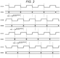
- FIG. 2 is a timing diagram of outputs of the CPLD 110.
- the CPLD 110 generates the clock signals CCA, CCB, CCC, and CCD whose phases are shifted by 90 degrees from each other, as shown in FIG. 2 , based on the system clock signal CA.
- the CPLD 110 takes in the drive data DBA output from the CPU 80 in synchronization with the clock signal CBA, buffers the drive data DBA, and outputs the drive data DBA to one of the drive circuits 12 in synchronization with the clock signal CCA.
- the drive circuit 12 receiving the drive data DBA and the clock signal CCA takes in the drive data DBA in synchronization with the clock signal CCA.
- the CPLD 110 takes in the drive data DBB output from the CPU 80 in synchronization with the clock signal CBB, buffers the drive data DBB, and outputs the drive data DBB to one of the drive circuits 12 in synchronization with the clock signal CCB.
- the drive circuit 12 receiving the drive data DBB and the clock signal CCB takes in the drive data DBB in synchronization with the clock signal CCB.
- the CPLD 110 takes in the drive data DBC output from the CPU 80 in synchronization with the clock signal CBC, buffers the drive data DBC, and outputs the drive data DBC to one of the drive circuits 12 in synchronization with the clock signal CCC.
- the drive circuit 12 receiving the drive data DBC and the clock signal CCC takes in the drive data DBC in synchronization with the clock signal CCC.
- the CPLD 110 takes in the drive data DBD output from the CPU 80 in synchronization with the clock signal CBD, buffers the drive data DBD, and outputs the drive data DBD to one of the drive circuits 12 in synchronization with the clock signal CCD.
- the drive circuit 12 receiving the drive data DBD and the clock signal CCD takes in the drive data DBD in synchronization with the clock signal CCD.
- Each of the four drive circuits 12 latches the taken-in drive data in synchronization with the latch signal LAT.
- Each of the four drive circuits 12 controls application of a current to the corresponding heating element 11 in synchronization with the strobe signal STB based on the drive data latched in this manner.
- the clock signals CBA, CBB, CBC, and CBD correspond to a plurality of first clock signals
- the clock signals CCA, CCB, CCC, and CCD correspond to a plurality of second clock signals.
- the CPU 80 also has a function as a drive data generation unit.
- the CPLD 110 has functions as a clock generation unit and a drive data supply unit.
- FIG. 3 is a diagram showing the state of fluctuations in a power supply current due to fluctuations in the clock signals CCA, CCB, CCC, and CCD.
- the state of fluctuations in the power supply current shown in FIG. 3 only represents the outline of a tendency of fluctuations, and minute fluctuations are not illustrated.
- Fluctuations in a power supply current due to fluctuations in the clock signal CCA are as in a current CUA shown in FIG. 3 .
- Fluctuations in a power supply current due to fluctuations in the clock signal CCB are as in a current CUB shown in FIG. 3 .
- Fluctuations in a power supply current due to fluctuations in the clock signal CCC are as in a current CUC shown in FIG. 3 .
- Fluctuations in a power supply current due to fluctuations in the clock signal CCD are as in a current CUD shown in FIG. 3 .
- the actual fluctuation in a power supply current CUX is a combination of these currents CUA, CUB, CUC, and CUD, and theoretically becomes zero as shown in FIG. 3 .
- the power supply current CUX does not become completely zero due to errors in change timings and signal levels of the clock signals CCA, CCB, CCC, and CCD, but it can be sufficiently reduced.
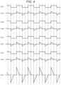
- FIG. 4 is a diagram showing the state of fluctuations in a power supply current if the clock signals CCA, CCB, CCC, and CCD fluctuate at the same timing.
- the state of fluctuations in the power supply current shown in FIG. 4 represents the outline of a tendency of fluctuations, and minute fluctuations are not illustrated.
- a phase difference between the clock signals CCA, CCB, CCC, and CCD is set to 90°, which is obtained by 4 / 360 because the number of groups of the heating elements 11 is four.
- This embodiment can be modified in various ways as follows.
- the number of groups of the heating elements 11 may be any integer equal to or greater than 2.
- n clock signals it is desirable that a phase difference between n clock signals be set to be an angle obtained by n / 360 as in the above-described embodiment.
- n clock signals have a phase difference, it is possible to reduce common-mode noise as compared to a case where there is no phase difference, and thus a phase difference of an angle different from an angle obtained by n / 360 may be provided.
- the functions implemented by the CPLD 110 can be partially or entirely implemented by hardware that executes processing that is not based on a program, such as a logic circuit.
Landscapes
- Electronic Switches (AREA)
Abstract
Description
- Embodiments described herein relate generally to a thermal printer.
- A thermal head configured such that a large number of mounted heating elements are divided into blocks, and drive data is input in parallel for each block is known.
- In a thermal printer using a thermal head having such a configuration, drive data for driving the heating elements of each block is input to the thermal head in synchronization with the same clock signal.
- For this reason, change timings of a plurality of pieces of drive data supplied to the thermal head may coincide with each other, leading to an increase in common-mode noise, which may cause a problem with electromagnetic interference (EMI).
- Due to such circumstances, it is desired to reduce common-mode noise.
- To this end, a thermal printer and a method of operating a thermal printer are provided.
-
-
FIG. 1 is a block diagram showing a circuit configuration of main parts of a thermal printer according to at least one embodiment; -
FIG. 2 is a timing diagram of outputs of a CPLD inFIG. 1 ; -
FIG. 3 is a diagram showing the state of fluctuations in a power supply current due to fluctuations in clock signals in at least one embodiment; and -
FIG. 4 is a diagram showing the state of fluctuations in a power supply current if clock signals fluctuate at the same timing. - There is provided a thermal printer that can reduce common-mode noise.
- In general, according to at least one embodiment, a thermal printer includes a thermal head, a drive data generation unit (drive data generator, a clock generation unit (clock generator), and a drive data supply unit (drive data supply). The thermal head is configured such that a large number of heating elements divided into a plurality of blocks are mounted thereon, and is configured to input drive data for driving the large number of heating elements to the plurality of blocks in parallel in synchronization with a plurality of different first clock signals (each of the plurality of first clock signals is different with respect to each of the plurality of blocks). The drive data generation unit is configured to generate a plurality of pieces of drive data for each of the plurality of blocks from print data and to output the plurality of pieces of drive data in synchronization with a plurality of second clock signals. The clock generation unit is configured to generate a plurality of clock signals whose phases are shifted from each other as the first clock signals. The drive data supply unit is configured to take in the plurality of pieces of drive data, which are output from the drive data generation unit, in synchronization with the plurality of second clock signals and to supply the plurality of pieces of drive data to the thermal head in synchronization with the plurality of first clock signals generated by the clock generation unit.
- An example of at least one embodiment will be described below with reference to the drawings.
-
FIG. 1 is a block diagram showing a circuit configuration of main parts of a thermal printer 1 according to at least one embodiment. - The thermal printer 1 includes a
thermal head 10, amotor group 20, amotor driver 30, asensor element group 40, asensor circuit 50, aclock generation circuit 60, aninput port 70, a central processing unit (CPU) 80, a read-only memory (ROM) 90, a random-access memory (RAM) 100, and a complex programmable logic device (CPLD) 110. - The
thermal head 10 includes a large number ofheating elements 11 and fourdrive circuits 12. All of the large number ofheating elements 11 generate heat by applying a current. The large number ofheating elements 11 are arranged, for example, in a row at equal intervals. However, the large number ofheating elements 11 may be arranged in multiple rows or in a zigzag manner. The large number ofheating elements 11 are divided into four groups. The fourdrive circuits 12 correspond to the four groups ofheating elements 11, respectively. Theheating elements 11 belonging to the corresponding group are connected to thedrive circuit 12. Thedrive circuit 12 controls application of a current to each of theheating elements 11 belonging to the corresponding group. - The
motor group 20 includes a plurality of motors. The motors included in themotor group 20 are power sources for conveying print paper and the like. - The
motor driver 30 drives the motors included in themotor group 20 under the control of theCPU 80. - The
sensor element group 40 includes various sensor elements for detecting an operating state of the thermal printer 1. - The
sensor circuit 50 determines the operating state of the thermal printer 1 based on the state of each of the sensor elements included in thesensor element group 40. - The
clock generation circuit 60 generates a system clock signal CA that serves as a reference for an operation timing of the thermal printer 1. - The
input port 70 is a port to which a host device is connected and through which print data transmitted from the host device is input. It is assumed that, for example, a well-known communication device based on a universal serial bus (USB) is used as theinput port 70. - The
CPU 80 generates four pieces of drive data DBA, DBB, DBC, and DBD for driving thethermal head 10 from the print data that is input through theinput port 70. TheCPU 80 outputs the drive data DBA, DBB, DBC, and DBD together with clock signals CBA, CBB, CBC, and CBD in synchronization with the clock signals CBA, CBB, CBC, and CBD having different timings. The pieces of drive data DBA, DBB, DBC, and DBD correspond to the four groups ofheating elements 11, respectively, and are supplied to thedrive circuits 12 corresponding to the same groups via theCPLD 110. - The
CPU 80 outputs a latch signal LAT for giving an instruction for a timing at which the drive data DBA, DBB, DBC, and DBD are latched to each of thedrive circuits 12 and a strobe signal STB for giving an instruction for a timing at which a current is applied to theheating elements 11 to each of the fourdrive circuits 12. - The
CPU 80 outputs the drive data DBA, DBB, DBC, and DBD, the latch signal LAT, and the strobe signal STB and controls themotor driver 30 in order to execute a necessary print operation while referring to the operating state determined by thesensor circuit 50. - The
ROM 90 stores various types of software that describe a processing procedure of theCPU 80 and various types of data to be referred to by theCPU 80 at the time of executing various types of information processing. - The
RAM 100 temporarily stores data used if theCPU 80 executes various types of information processing. - The
CPLD 110 is programed to constitute a logic circuit for generating clock signals CCA, CCB, CCC, and CCD to be described later and supplying the drive data DBA, DBB, DBC, and DBD to thethermal head 10 in synchronization with the clock signals CCA, CCB, CCC, and CCD. - Next, an operation of the thermal printer 1 configured as described above will be described.
- An operation of printing an image using the thermal printer 1 may be basically the same as that of other existing thermal printers of the same type. An operation of the thermal printer 1 which is different from those of other existing thermal printers is the supply of the drive data DBA, DBB, DBC, and DBD to the
thermal head 10, which will be described below. -
FIG. 2 is a timing diagram of outputs of theCPLD 110. - The
CPLD 110 generates the clock signals CCA, CCB, CCC, and CCD whose phases are shifted by 90 degrees from each other, as shown inFIG. 2 , based on the system clock signal CA. - The
CPLD 110 takes in the drive data DBA output from theCPU 80 in synchronization with the clock signal CBA, buffers the drive data DBA, and outputs the drive data DBA to one of thedrive circuits 12 in synchronization with the clock signal CCA. Thedrive circuit 12 receiving the drive data DBA and the clock signal CCA takes in the drive data DBA in synchronization with the clock signal CCA. - The
CPLD 110 takes in the drive data DBB output from theCPU 80 in synchronization with the clock signal CBB, buffers the drive data DBB, and outputs the drive data DBB to one of thedrive circuits 12 in synchronization with the clock signal CCB. Thedrive circuit 12 receiving the drive data DBB and the clock signal CCB takes in the drive data DBB in synchronization with the clock signal CCB. - The
CPLD 110 takes in the drive data DBC output from theCPU 80 in synchronization with the clock signal CBC, buffers the drive data DBC, and outputs the drive data DBC to one of thedrive circuits 12 in synchronization with the clock signal CCC. Thedrive circuit 12 receiving the drive data DBC and the clock signal CCC takes in the drive data DBC in synchronization with the clock signal CCC. - The
CPLD 110 takes in the drive data DBD output from theCPU 80 in synchronization with the clock signal CBD, buffers the drive data DBD, and outputs the drive data DBD to one of thedrive circuits 12 in synchronization with the clock signal CCD. Thedrive circuit 12 receiving the drive data DBD and the clock signal CCD takes in the drive data DBD in synchronization with the clock signal CCD. - Each of the four
drive circuits 12 latches the taken-in drive data in synchronization with the latch signal LAT. Each of the fourdrive circuits 12 controls application of a current to thecorresponding heating element 11 in synchronization with the strobe signal STB based on the drive data latched in this manner. - As described above, the clock signals CBA, CBB, CBC, and CBD correspond to a plurality of first clock signals, and the clock signals CCA, CCB, CCC, and CCD correspond to a plurality of second clock signals. The
CPU 80 also has a function as a drive data generation unit. TheCPLD 110 has functions as a clock generation unit and a drive data supply unit. -
FIG. 3 is a diagram showing the state of fluctuations in a power supply current due to fluctuations in the clock signals CCA, CCB, CCC, and CCD. However, the state of fluctuations in the power supply current shown inFIG. 3 only represents the outline of a tendency of fluctuations, and minute fluctuations are not illustrated. - Fluctuations in a power supply current due to fluctuations in the clock signal CCA are as in a current CUA shown in
FIG. 3 . Fluctuations in a power supply current due to fluctuations in the clock signal CCB are as in a current CUB shown inFIG. 3 . Fluctuations in a power supply current due to fluctuations in the clock signal CCC are as in a current CUC shown inFIG. 3 . Fluctuations in a power supply current due to fluctuations in the clock signal CCD are as in a current CUD shown inFIG. 3 . However, the actual fluctuation in a power supply current CUX is a combination of these currents CUA, CUB, CUC, and CUD, and theoretically becomes zero as shown inFIG. 3 . However, actually, the power supply current CUX does not become completely zero due to errors in change timings and signal levels of the clock signals CCA, CCB, CCC, and CCD, but it can be sufficiently reduced. -
FIG. 4 is a diagram showing the state of fluctuations in a power supply current if the clock signals CCA, CCB, CCC, and CCD fluctuate at the same timing. However, the state of fluctuations in the power supply current shown inFIG. 4 represents the outline of a tendency of fluctuations, and minute fluctuations are not illustrated. - As shown in
FIG. 4 , if the clock signals CCA, CCB, CCC, and CCD fluctuate at the same timing, fluctuations in the power supply current CUX become significantly large, and it can be understood that fluctuations in the power supply current CUX can be significantly reduced in the embodiment. - Thus, according to the thermal printer 1, it is possible to reduce common-mode noise.
- In the thermal printer 1, a phase difference between the clock signals CCA, CCB, CCC, and CCD is set to 90°, which is obtained by 4 / 360 because the number of groups of the
heating elements 11 is four. Thereby, as described above, fluctuations in the power supply current CUX can be logically set to zero, and common-mode noise can be minimized. - This embodiment can be modified in various ways as follows.
- The number of groups of the
heating elements 11 may be any integer equal to or greater than 2. - If the number of groups of the
heating elements 11 is expressed as n, it is desirable that a phase difference between n clock signals be set to be an angle obtained by n / 360 as in the above-described embodiment. However, if the n clock signals have a phase difference, it is possible to reduce common-mode noise as compared to a case where there is no phase difference, and thus a phase difference of an angle different from an angle obtained by n / 360 may be provided. - The functions implemented by the
CPLD 110 can be partially or entirely implemented by hardware that executes processing that is not based on a program, such as a logic circuit. - While certain embodiments have been described, these embodiments have been presented by way of example only, and are not intended to limit the scope of the disclosure. Indeed, the novel embodiment described herein may be embodied in a variety of other forms; furthermore, various omissions, substitutions and changes in the form of the embodiments described herein may be made without departing from the scope of the disclosure. The accompanying claims and their equivalents are intended to cover such forms or modifications as would fall within the scope of the disclosure.
Claims (10)
- A thermal printer comprising:a thermal head arranged such that a large number of heating elements divided into a plurality of blocks are mounted on the thermal head, the thermal head configured to input drive data for driving the large number of heating elements to the plurality of blocks in parallel in synchronization with a plurality of different first clock signals;a drive data generator configured to:generate a plurality of pieces of drive data for each of the plurality of blocks from print data, andoutput the plurality of pieces of drive data in synchronization with a plurality of second clock signals;a clock generator configured to generate a plurality of clock signals whose phases are shifted from each other as the first clock signals; anda drive data supply configured to:take in the plurality of pieces of drive data, which are output from the drive data generator, in synchronization with the plurality of second clock signals, andsupply the plurality of pieces of drive data to the thermal head in synchronization with the plurality of first clock signals generated by the clock generator.
- The printer according to claim 1, whereinthe large number of heating elements divided into n (n is an integer) blocks are mounted on the thermal head, andthe clock generator is configured to generate n first clock signals whose phases are different by 360 / n degrees.
- The printer according to claim 1 or 2, wherein the large number of heating elements are arranged in a row in equal intervals.
- The printer according to any one of claims 1 to 3, wherein the large number of heating elements are arranged in multiple rows or in a zigzag manner.
- The printer according to any one of claims 1 to 4, wherein a number of groups of the heating elements may be any integer equal to or greater than 2.
- A method of operating a thermal printer, the thermal printed comprising:a thermal head arranged such that a large number of heating elements divided into a plurality of blocks are mounted on the thermal head, the thermal head configured to input drive data for driving the large number of heating elements to the plurality of blocks in parallel in synchronization with a plurality of different first clock signals,the method comprising:generating a plurality of pieces of drive data for each of the plurality of blocks from print data;
outputting the plurality of pieces of drive data in synchronization with a plurality of second clock signals;generating a plurality of clock signals whose phases are shifted from each other as the first clock signals;taking in the plurality of pieces of drive data, which are output, in synchronization with the plurality of second clock signals; andsupplying the plurality of pieces of drive data to the thermal head in synchronization with the plurality of first clock signals generated by the clock generator. - The method according to claim 6, wherein
the large number of heating elements divided into n (n is an integer) blocks are mounted on the thermal head, and further comprising generating n first clock signals whose phases are different by 360 / n degrees. - The method according to claim 6 or 7, wherein the large number of heating elements are arranged in a row in equal intervals.
- The method according to any one of claims 6 to 8, wherein the large number of heating elements are arranged in multiple rows or in a zigzag manner.
- The method according to any one of claims 6 to 9, wherein a number of groups of the heating elements may be any integer equal to or greater than 2.
Applications Claiming Priority (1)
| Application Number | Priority Date | Filing Date | Title |
|---|---|---|---|
| JP2023068573A JP7828922B2 (en) | 2023-04-19 | 2023-04-19 | Thermal printer |
Publications (2)
| Publication Number | Publication Date |
|---|---|
| EP4450290A1 true EP4450290A1 (en) | 2024-10-23 |
| EP4450290B1 EP4450290B1 (en) | 2026-03-04 |
Family
ID=90053730
Family Applications (1)
| Application Number | Title | Priority Date | Filing Date |
|---|---|---|---|
| EP24159060.3A Active EP4450290B1 (en) | 2023-04-19 | 2024-02-22 | Thermal printer |
Country Status (4)
| Country | Link |
|---|---|
| US (1) | US12508819B2 (en) |
| EP (1) | EP4450290B1 (en) |
| JP (1) | JP7828922B2 (en) |
| CN (1) | CN118810249B (en) |
Citations (1)
| Publication number | Priority date | Publication date | Assignee | Title |
|---|---|---|---|---|
| JP2008155491A (en) * | 2006-12-25 | 2008-07-10 | Seiko Epson Corp | Thermal head driver, thermal head, electronic equipment and printing system |
Family Cites Families (14)
| Publication number | Priority date | Publication date | Assignee | Title |
|---|---|---|---|---|
| JP2798933B2 (en) * | 1988-07-28 | 1998-09-17 | 株式会社東芝 | Recording device |
| JP2938275B2 (en) * | 1991-10-31 | 1999-08-23 | 京セラ株式会社 | Printing device |
| JPH0796622A (en) * | 1993-06-30 | 1995-04-11 | Kyocera Corp | Printing device drive method |
| JPH07125286A (en) * | 1993-10-29 | 1995-05-16 | Kyocera Corp | Thermal head |
| JP3310789B2 (en) * | 1994-09-06 | 2002-08-05 | 富士写真フイルム株式会社 | Color thermal printing method |
| JPH08300711A (en) * | 1995-05-15 | 1996-11-19 | Tec Corp | Method of inputting multi-gradation data to line head |
| JPH10193617A (en) * | 1996-11-14 | 1998-07-28 | Canon Inc | Recording apparatus and its control |
| JP2001301211A (en) * | 2000-04-19 | 2001-10-30 | Seiko Epson Corp | Thermal head control device and head drive IC |
| KR100365691B1 (en) * | 2000-08-17 | 2002-12-26 | 삼성전자 주식회사 | Circuit and method for driving thermal print head quickly |
| JP2008279683A (en) | 2007-05-11 | 2008-11-20 | Shinko Electric Co Ltd | Printer, printer control method, printer control program |
| JP5072578B2 (en) * | 2007-12-21 | 2012-11-14 | キヤノン株式会社 | Head element substrate, recording head, and recording apparatus |
| JP2014058051A (en) * | 2012-09-14 | 2014-04-03 | Oki Data Corp | Light emitting element unit substrate, and exposure unit and image formation device including the same |
| JP6302880B2 (en) * | 2015-08-31 | 2018-03-28 | 東芝テック株式会社 | Thermal printer |
| CN112590402B (en) * | 2020-12-11 | 2022-02-22 | 南阳柯丽尔科技有限公司 | Thermal printer control method, thermal printer control device, thermal printer and medium |
-
2023
- 2023-04-19 JP JP2023068573A patent/JP7828922B2/en active Active
-
2024
- 2024-02-06 US US18/434,264 patent/US12508819B2/en active Active
- 2024-02-18 CN CN202410181107.4A patent/CN118810249B/en active Active
- 2024-02-22 EP EP24159060.3A patent/EP4450290B1/en active Active
Patent Citations (1)
| Publication number | Priority date | Publication date | Assignee | Title |
|---|---|---|---|---|
| JP2008155491A (en) * | 2006-12-25 | 2008-07-10 | Seiko Epson Corp | Thermal head driver, thermal head, electronic equipment and printing system |
Also Published As
| Publication number | Publication date |
|---|---|
| CN118810249B (en) | 2026-08-04 |
| US12508819B2 (en) | 2025-12-30 |
| CN118810249A (en) | 2024-10-22 |
| US20240351348A1 (en) | 2024-10-24 |
| JP2024154640A (en) | 2024-10-31 |
| EP4450290B1 (en) | 2026-03-04 |
| JP7828922B2 (en) | 2026-03-12 |
Similar Documents
| Publication | Publication Date | Title |
|---|---|---|
| CN1318881C (en) | Beam light scanning device and image forming apparatus using same | |
| EP2072260B1 (en) | Head element substrate, recording head, and recording apparatus | |
| CN101879817B (en) | Printer and control method for a printer | |
| JP6314982B2 (en) | Image forming apparatus and phase adjustment method | |
| JP2010162810A5 (en) | ||
| EP4450290B1 (en) | Thermal printer | |
| JPS5831785A (en) | Control mode for printer | |
| US7452041B2 (en) | Ink jet heater chip with internally generated clock signal | |
| US6752480B2 (en) | Integrated-circuit apparatus and ink jet recording apparatus using the same | |
| CN112590402B (en) | Thermal printer control method, thermal printer control device, thermal printer and medium | |
| US12030323B2 (en) | Interface circuit and thermal history control method | |
| US9070078B2 (en) | Transfer system and printing apparatus | |
| JP2011235528A (en) | Recording head and recording apparatus | |
| JP4079958B2 (en) | Thermal history control device, operation method thereof, and thermal printer | |
| JP3182789B2 (en) | Printer control device, printer and control method therefor | |
| JP5013704B2 (en) | Multi-beam image output device and method for controlling image output device | |
| EP4520537A1 (en) | Thermal printer and control method thereof | |
| JP2008078800A (en) | Image forming apparatus | |
| JPH04327952A (en) | Printing by printer | |
| JP3222971B2 (en) | Serial dot printer | |
| JP2009096078A (en) | Thermal printer and print control method | |
| JP2563014B2 (en) | Thermal head | |
| JPH01115644A (en) | Recording head device | |
| JP2015166972A (en) | Transfer system and printing device | |
| JP2015166973A (en) | Transfer system and printing device |
Legal Events
| Date | Code | Title | Description |
|---|---|---|---|
| PUAI | Public reference made under article 153(3) epc to a published international application that has entered the european phase |
Free format text: ORIGINAL CODE: 0009012 |
|
| STAA | Information on the status of an ep patent application or granted ep patent |
Free format text: STATUS: THE APPLICATION HAS BEEN PUBLISHED |
|
| AK | Designated contracting states |
Kind code of ref document: A1 Designated state(s): AL AT BE BG CH CY CZ DE DK EE ES FI FR GB GR HR HU IE IS IT LI LT LU LV MC ME MK MT NL NO PL PT RO RS SE SI SK SM TR |
|
| STAA | Information on the status of an ep patent application or granted ep patent |
Free format text: STATUS: REQUEST FOR EXAMINATION WAS MADE |
|
| 17P | Request for examination filed |
Effective date: 20250423 |
|
| GRAP | Despatch of communication of intention to grant a patent |
Free format text: ORIGINAL CODE: EPIDOSNIGR1 |
|
| STAA | Information on the status of an ep patent application or granted ep patent |
Free format text: STATUS: GRANT OF PATENT IS INTENDED |
|
| INTG | Intention to grant announced |
Effective date: 20250924 |
|
| GRAS | Grant fee paid |
Free format text: ORIGINAL CODE: EPIDOSNIGR3 |
|
| GRAA | (expected) grant |
Free format text: ORIGINAL CODE: 0009210 |
|
| STAA | Information on the status of an ep patent application or granted ep patent |
Free format text: STATUS: THE PATENT HAS BEEN GRANTED |
|
| AK | Designated contracting states |
Kind code of ref document: B1 Designated state(s): AL AT BE BG CH CY CZ DE DK EE ES FI FR GB GR HR HU IE IS IT LI LT LU LV MC ME MK MT NL NO PL PT RO RS SE SI SK SM TR |
|
| REG | Reference to a national code |
Ref country code: CH Ref legal event code: F10 Free format text: ST27 STATUS EVENT CODE: U-0-0-F10-F00 (AS PROVIDED BY THE NATIONAL OFFICE) Effective date: 20260304 Ref country code: GB Ref legal event code: FG4D |
|
| REG | Reference to a national code |
Ref country code: IE Ref legal event code: FG4D |
|
| REG | Reference to a national code |
Ref country code: DE Ref legal event code: R096 Ref document number: 602024002885 Country of ref document: DE |
|
| PG25 | Lapsed in a contracting state [announced via postgrant information from national office to epo] |
Ref country code: RS Free format text: LAPSE BECAUSE OF FAILURE TO SUBMIT A TRANSLATION OF THE DESCRIPTION OR TO PAY THE FEE WITHIN THE PRESCRIBED TIME-LIMIT Effective date: 20260604 |
|
| PG25 | Lapsed in a contracting state [announced via postgrant information from national office to epo] |
Ref country code: ES Free format text: LAPSE BECAUSE OF FAILURE TO SUBMIT A TRANSLATION OF THE DESCRIPTION OR TO PAY THE FEE WITHIN THE PRESCRIBED TIME-LIMIT Effective date: 20260304 |
|
| REG | Reference to a national code |
Ref country code: NL Ref legal event code: MP Effective date: 20260304 |
|
| PG25 | Lapsed in a contracting state [announced via postgrant information from national office to epo] |
Ref country code: PL Free format text: LAPSE BECAUSE OF FAILURE TO SUBMIT A TRANSLATION OF THE DESCRIPTION OR TO PAY THE FEE WITHIN THE PRESCRIBED TIME-LIMIT Effective date: 20260304 |
|
| PG25 | Lapsed in a contracting state [announced via postgrant information from national office to epo] |
Ref country code: GR Free format text: LAPSE BECAUSE OF FAILURE TO SUBMIT A TRANSLATION OF THE DESCRIPTION OR TO PAY THE FEE WITHIN THE PRESCRIBED TIME-LIMIT Effective date: 20260605 |
|
| REG | Reference to a national code |
Ref country code: LT Ref legal event code: MG9D |
|
| PG25 | Lapsed in a contracting state [announced via postgrant information from national office to epo] |
Ref country code: LT Free format text: LAPSE BECAUSE OF FAILURE TO SUBMIT A TRANSLATION OF THE DESCRIPTION OR TO PAY THE FEE WITHIN THE PRESCRIBED TIME-LIMIT Effective date: 20260304 |
|
| PG25 | Lapsed in a contracting state [announced via postgrant information from national office to epo] |
Ref country code: NO Free format text: LAPSE BECAUSE OF FAILURE TO SUBMIT A TRANSLATION OF THE DESCRIPTION OR TO PAY THE FEE WITHIN THE PRESCRIBED TIME-LIMIT Effective date: 20260604 |
|
| PG25 | Lapsed in a contracting state [announced via postgrant information from national office to epo] |
Ref country code: SE Free format text: LAPSE BECAUSE OF FAILURE TO SUBMIT A TRANSLATION OF THE DESCRIPTION OR TO PAY THE FEE WITHIN THE PRESCRIBED TIME-LIMIT Effective date: 20260304 Ref country code: FI Free format text: LAPSE BECAUSE OF FAILURE TO SUBMIT A TRANSLATION OF THE DESCRIPTION OR TO PAY THE FEE WITHIN THE PRESCRIBED TIME-LIMIT Effective date: 20260304 |
|
| PG25 | Lapsed in a contracting state [announced via postgrant information from national office to epo] |
Ref country code: HR Free format text: LAPSE BECAUSE OF FAILURE TO SUBMIT A TRANSLATION OF THE DESCRIPTION OR TO PAY THE FEE WITHIN THE PRESCRIBED TIME-LIMIT Effective date: 20260304 |
|
| PG25 | Lapsed in a contracting state [announced via postgrant information from national office to epo] |
Ref country code: LV Free format text: LAPSE BECAUSE OF FAILURE TO SUBMIT A TRANSLATION OF THE DESCRIPTION OR TO PAY THE FEE WITHIN THE PRESCRIBED TIME-LIMIT Effective date: 20260304 |
|
| PG25 | Lapsed in a contracting state [announced via postgrant information from national office to epo] |
Ref country code: BG Free format text: LAPSE BECAUSE OF FAILURE TO SUBMIT A TRANSLATION OF THE DESCRIPTION OR TO PAY THE FEE WITHIN THE PRESCRIBED TIME-LIMIT Effective date: 20260304 |