EP4447028A1 - Tiled display device - Google Patents
Tiled display device Download PDFInfo
- Publication number
- EP4447028A1 EP4447028A1 EP21966992.6A EP21966992A EP4447028A1 EP 4447028 A1 EP4447028 A1 EP 4447028A1 EP 21966992 A EP21966992 A EP 21966992A EP 4447028 A1 EP4447028 A1 EP 4447028A1
- Authority
- EP
- European Patent Office
- Prior art keywords
- fastening
- elements
- magnetic
- display device
- modules
- Prior art date
- Legal status (The legal status is an assumption and is not a legal conclusion. Google has not performed a legal analysis and makes no representation as to the accuracy of the status listed.)
- Pending
Links
Images


Classifications
-
- G—PHYSICS
- G09—EDUCATION; CRYPTOGRAPHY; DISPLAY; ADVERTISING; SEALS
- G09F—DISPLAYING; ADVERTISING; SIGNS; LABELS OR NAME-PLATES; SEALS
- G09F9/00—Indicating arrangements for variable information in which the information is built-up on a support by selection or combination of individual elements
- G09F9/30—Indicating arrangements for variable information in which the information is built-up on a support by selection or combination of individual elements in which the desired character or characters are formed by combining individual elements
- G09F9/302—Indicating arrangements for variable information in which the information is built-up on a support by selection or combination of individual elements in which the desired character or characters are formed by combining individual elements characterised by the form or geometrical disposition of the individual elements
-
- G—PHYSICS
- G02—OPTICS
- G02F—OPTICAL DEVICES OR ARRANGEMENTS FOR THE CONTROL OF LIGHT BY MODIFICATION OF THE OPTICAL PROPERTIES OF THE MEDIA OF THE ELEMENTS INVOLVED THEREIN; NON-LINEAR OPTICS; FREQUENCY-CHANGING OF LIGHT; OPTICAL LOGIC ELEMENTS; OPTICAL ANALOGUE/DIGITAL CONVERTERS
- G02F1/00—Devices or arrangements for the control of the intensity, colour, phase, polarisation or direction of light arriving from an independent light source, e.g. switching, gating or modulating; Non-linear optics
- G02F1/01—Devices or arrangements for the control of the intensity, colour, phase, polarisation or direction of light arriving from an independent light source, e.g. switching, gating or modulating; Non-linear optics for the control of the intensity, phase, polarisation or colour
- G02F1/13—Devices or arrangements for the control of the intensity, colour, phase, polarisation or direction of light arriving from an independent light source, e.g. switching, gating or modulating; Non-linear optics for the control of the intensity, phase, polarisation or colour based on liquid crystals, e.g. single liquid crystal display cells
- G02F1/133—Constructional arrangements; Operation of liquid crystal cells; Circuit arrangements
- G02F1/1333—Constructional arrangements; Manufacturing methods
- G02F1/13336—Combining plural substrates to produce large-area displays, e.g. tiled displays
-
- G—PHYSICS
- G02—OPTICS
- G02F—OPTICAL DEVICES OR ARRANGEMENTS FOR THE CONTROL OF LIGHT BY MODIFICATION OF THE OPTICAL PROPERTIES OF THE MEDIA OF THE ELEMENTS INVOLVED THEREIN; NON-LINEAR OPTICS; FREQUENCY-CHANGING OF LIGHT; OPTICAL LOGIC ELEMENTS; OPTICAL ANALOGUE/DIGITAL CONVERTERS
- G02F1/00—Devices or arrangements for the control of the intensity, colour, phase, polarisation or direction of light arriving from an independent light source, e.g. switching, gating or modulating; Non-linear optics
- G02F1/01—Devices or arrangements for the control of the intensity, colour, phase, polarisation or direction of light arriving from an independent light source, e.g. switching, gating or modulating; Non-linear optics for the control of the intensity, phase, polarisation or colour
- G02F1/13—Devices or arrangements for the control of the intensity, colour, phase, polarisation or direction of light arriving from an independent light source, e.g. switching, gating or modulating; Non-linear optics for the control of the intensity, phase, polarisation or colour based on liquid crystals, e.g. single liquid crystal display cells
- G02F1/133—Constructional arrangements; Operation of liquid crystal cells; Circuit arrangements
- G02F1/1333—Constructional arrangements; Manufacturing methods
- G02F1/133308—Support structures for LCD panels, e.g. frames or bezels
- G02F1/133314—Back frames
-
- G—PHYSICS
- G06—COMPUTING OR CALCULATING; COUNTING
- G06F—ELECTRIC DIGITAL DATA PROCESSING
- G06F3/00—Input arrangements for transferring data to be processed into a form capable of being handled by the computer; Output arrangements for transferring data from processing unit to output unit, e.g. interface arrangements
- G06F3/14—Digital output to display device ; Cooperation and interconnection of the display device with other functional units
- G06F3/1423—Digital output to display device ; Cooperation and interconnection of the display device with other functional units controlling a plurality of local displays, e.g. CRT and flat panel display
- G06F3/1446—Digital output to display device ; Cooperation and interconnection of the display device with other functional units controlling a plurality of local displays, e.g. CRT and flat panel display display composed of modules, e.g. video walls
-
- G—PHYSICS
- G09—EDUCATION; CRYPTOGRAPHY; DISPLAY; ADVERTISING; SEALS
- G09F—DISPLAYING; ADVERTISING; SIGNS; LABELS OR NAME-PLATES; SEALS
- G09F9/00—Indicating arrangements for variable information in which the information is built-up on a support by selection or combination of individual elements
- G09F9/30—Indicating arrangements for variable information in which the information is built-up on a support by selection or combination of individual elements in which the desired character or characters are formed by combining individual elements
- G09F9/302—Indicating arrangements for variable information in which the information is built-up on a support by selection or combination of individual elements in which the desired character or characters are formed by combining individual elements characterised by the form or geometrical disposition of the individual elements
- G09F9/3026—Video wall, i.e. stackable semiconductor matrix display modules
-
- G—PHYSICS
- G09—EDUCATION; CRYPTOGRAPHY; DISPLAY; ADVERTISING; SEALS
- G09F—DISPLAYING; ADVERTISING; SIGNS; LABELS OR NAME-PLATES; SEALS
- G09F9/00—Indicating arrangements for variable information in which the information is built-up on a support by selection or combination of individual elements
- G09F9/30—Indicating arrangements for variable information in which the information is built-up on a support by selection or combination of individual elements in which the desired character or characters are formed by combining individual elements
- G09F9/33—Indicating arrangements for variable information in which the information is built-up on a support by selection or combination of individual elements in which the desired character or characters are formed by combining individual elements being semiconductor devices, e.g. diodes
-
- G—PHYSICS
- G09—EDUCATION; CRYPTOGRAPHY; DISPLAY; ADVERTISING; SEALS
- G09F—DISPLAYING; ADVERTISING; SIGNS; LABELS OR NAME-PLATES; SEALS
- G09F9/00—Indicating arrangements for variable information in which the information is built-up on a support by selection or combination of individual elements
- G09F9/30—Indicating arrangements for variable information in which the information is built-up on a support by selection or combination of individual elements in which the desired character or characters are formed by combining individual elements
- G09F9/35—Indicating arrangements for variable information in which the information is built-up on a support by selection or combination of individual elements in which the desired character or characters are formed by combining individual elements being liquid crystals
-
- G—PHYSICS
- G02—OPTICS
- G02F—OPTICAL DEVICES OR ARRANGEMENTS FOR THE CONTROL OF LIGHT BY MODIFICATION OF THE OPTICAL PROPERTIES OF THE MEDIA OF THE ELEMENTS INVOLVED THEREIN; NON-LINEAR OPTICS; FREQUENCY-CHANGING OF LIGHT; OPTICAL LOGIC ELEMENTS; OPTICAL ANALOGUE/DIGITAL CONVERTERS
- G02F2201/00—Constructional arrangements not provided for in groups G02F1/00 - G02F7/00
- G02F2201/46—Fixing elements
-
- H—ELECTRICITY
- H10—SEMICONDUCTOR DEVICES; ELECTRIC SOLID-STATE DEVICES NOT OTHERWISE PROVIDED FOR
- H10K—ORGANIC ELECTRIC SOLID-STATE DEVICES
- H10K59/00—Integrated devices, or assemblies of multiple devices, comprising at least one organic light-emitting element covered by group H10K50/00
- H10K59/10—OLED displays
- H10K59/12—Active-matrix OLED [AMOLED] displays
- H10K59/1201—Manufacture or treatment
-
- H—ELECTRICITY
- H10—SEMICONDUCTOR DEVICES; ELECTRIC SOLID-STATE DEVICES NOT OTHERWISE PROVIDED FOR
- H10W—GENERIC PACKAGES, INTERCONNECTIONS, CONNECTORS OR OTHER CONSTRUCTIONAL DETAILS OF DEVICES COVERED BY CLASS H10
- H10W90/00—Package configurations
-
- Y—GENERAL TAGGING OF NEW TECHNOLOGICAL DEVELOPMENTS; GENERAL TAGGING OF CROSS-SECTIONAL TECHNOLOGIES SPANNING OVER SEVERAL SECTIONS OF THE IPC; TECHNICAL SUBJECTS COVERED BY FORMER USPC CROSS-REFERENCE ART COLLECTIONS [XRACs] AND DIGESTS
- Y02—TECHNOLOGIES OR APPLICATIONS FOR MITIGATION OR ADAPTATION AGAINST CLIMATE CHANGE
- Y02E—REDUCTION OF GREENHOUSE GAS [GHG] EMISSIONS, RELATED TO ENERGY GENERATION, TRANSMISSION OR DISTRIBUTION
- Y02E10/00—Energy generation through renewable energy sources
- Y02E10/50—Photovoltaic [PV] energy
Definitions
- the present disclosure relates to a field of display technology and in particular, to a splicing display device.
- the inventor of the present disclosure found that the light-emitting diode light bars are generally fixed on the liquid crystal panels with an adhesive, which is not conducive to the installation and adjustment of the light-emitting diode light bars.
- the present disclosure provides a splicing display device, which facilitates the installation and adjustment of a light-emitting diode substrate.
- the present disclosure provides a splicing display device, characterized by including:
- each of the magnetic assemblies includes a supporting base, a connecting element, and a second magnetic member, supporting bases of the magnetic assemblies are arranged on the fastening elements, connecting elements of the magnetic assemblies are extendably arranged on the supporting bases, and second magnetic members of the magnetic assemblies are arranged on the connecting elements.
- each of the connecting elements and a corresponding second magnetic member of the second magnetic members are integrally formed, and each of the connecting elements is made of a magnetic material.
- each of the supporting bases is provided with a threaded hole
- an outer surface of each of the connecting elements is provided with a plurality of threads
- the connecting elements are threadedly connected to threaded holes of the supporting bases.
- one end of each of the fastening elements is connected to a back of one of the support modules, and another end of each of the fastening elements is connected to a back of another one of the support modules, and each of the fastening elements crosses a corresponding gap of the gaps; and each of the connecting elements is arranged on a portion of one of the fastening elements corresponding to one of the gaps.
- each of the fastening elements is disposed in one of the gaps, one end of each of the fastening elements is connected to a side surface of one of the support modules, and another end of each fastening element is connected to a side surface of another one of the support modules, or.
- each of the fastening elements includes a first fastening part and a second fastening part
- each of the connecting elements includes a first connecting part and a second connecting part, between two adjacent ones of the at least two display devices, the first fastening part is arranged on a back or a side surface of one of the support modules, and the second fastening part is arranged on a back or a side surface of another one of the support modules, the first connecting part is arranged on the first fastening part, and the second connecting part is arranged on the second fastening part.
- the support modules are backlight modules, and panels of the at least two display devices are liquid crystal panels.
- each of the support modules includes a backplate
- panels of the at least two display devices are non-liquid-crystal panels
- the panels are arranged on backplates of the support modules
- the fastening elements are arranged on sides of the backplates away from the panels.
- the present disclosure further provides a splicing display device, characterized by including:
- the present disclosure uses the fastening modules and the first magnetic members arranged on the LED substrates to achieve magnetic attraction connection, which simplifies installation of the LED substrates and enhances adjustability of the LED substrates.
- a plurality of redundant bond pads are arranged on each base of the LED substrates, the redundant bond pads are arranged on one side of each base away from the corresponding LED elements, and the first magnetic members are fixedly connected to the redundant bond pads.
- the first magnetic members are fixed on the redundant bond pads.
- idle bond pads are reasonably used.
- the welding method is used to achieve stable connection between the first magnetic members and the redundant bond pads.
- each of the magnetic assemblies includes a supporting base, a connecting element, and a second magnetic member, supporting bases of the magnetic assemblies are arranged on the fastening elements, connecting elements of the magnetic assemblies are extendably arranged on the supporting bases, and second magnetic members of the magnetic assemblies are arranged on the connecting elements.
- the connecting element is extendably arranged on the supporting base, and therefore the present disclosure can easily adjust a vertical position of the LED substrate, and improves the stability and applicability in installing the LED substrate.
- each of the connecting elements and a corresponding second magnetic member of the second magnetic members are integrally formed, and each of the connecting elements is made of a magnetic material.
- Such configuration simplifies a structure of the magnetic assembly and improves the stability of the overall structure.
- each of the supporting bases is provided with a threaded hole
- an outer surface of each of the connecting elements is provided with a plurality of threads
- the connecting elements are threadedly connected to threaded holes of the supporting bases.
- the connecting element is extendable by means of a threaded connection, and the threaded connection achieves precise extendable functions and a convenient telescopic extension of the connecting element.
- one end of each of the fastening elements is connected to a back of one of the support modules, and another end of each of the fastening elements is connected to a back of another one of the support modules, and each of the fastening elements crosses a corresponding gap of the gaps; and each of the connecting elements is arranged on a portion of one of the fastening elements corresponding to one of the gaps.
- the fastening element is fixed to the backs of the support modules of two adjacent display devices, thereby improving the stability and convenience in assembling the fastening module and the display devices.
- each of the fastening elements is disposed in one of the gaps, one end of each of the fastening elements is connected to a side surface of one of the support modules, and another end of each fastening element is connected to a side surface of another one of the support modules.
- the fastening element is fixed to the side surfaces of the support modules of two adjacent display devices and is located in the gap.
- the present disclosure improves the stability of an assembled structure of the fastening module and the display device and saves installation space.
- each of the fastening elements includes a first fastening part and a second fastening part
- each of the connecting elements includes a first connecting part and a second connecting part, between two adjacent ones of the at least two display devices, the first fastening part is arranged on a back or a side surface of one of the support modules, and the second fastening part is arranged on a back or a side surface of another one of the support modules, the first connecting part is arranged on the first fastening part, and the second connecting part is arranged on the second fastening part.
- One fastening element is installed corresponding to one connecting element, so difficulty of maintenance is reduced.
- the support modules are backlight modules, and panels of the at least two display devices are liquid crystal panels.
- the present disclosure combines liquid crystal display devices and the LED substrates, thus reducing costs of the splicing display device.
- each of the support modules includes a backplate
- panels of the at least two display devices are non-liquid-crystal panels
- the panels are arranged on backplates of the support modules
- the fastening elements are arranged on sides of the backplates away from the panels.
- each of the first magnetic members includes a material selected from one of a magnetic conductor material or a permanent magnetic material.
- the splicing display device of the present disclosure includes at least two display devices, a plurality of LED substrates, and a plurality of fastening modules.
- a plurality of gaps are defined between the at least two display devices, and each display device includes a support module and a panel disposed on the support module.
- Each LED substrate is arranged on two adjacent display devices and covers one of the gaps.
- the LED substrate includes a base, a plurality of LED elements and a plurality of first magnetic members, the LED elements are arranged on the base, and the first magnetic members are arranged on one side of the base away from the LED elements.
- Each fastening module includes a fastening element and a plurality of magnetic assemblies, the fastening elements are arranged on the support modules, at least a portion of each fastening element is arranged corresponding to one of the gaps, the magnetic assemblies are arranged on the fastening elements and located in the plurality of gaps, and the magnetic assemblies are magnetically connected to the first magnetic members.
- the present disclosure uses the fastening modules and the first magnetic members arranged on the LED substrates to achieve magnetic attraction connection, which simplifies installation of the LED substrates and enhances adjustability of the LED substrates.
- the present disclosure provides a splicing display device. Detailed descriptions are provided below. It should be noted that an order of descriptions in the following embodiments is not intended to limit a preferred order of the embodiments.
- an embodiment of the present disclosure provides a splicing display device 1000.
- the splicing display device 1000 includes at least two display devices 100, a plurality of light-emitting diode (LED) substrates 200 and a plurality of fastening modules 300.
- LED light-emitting diode
- At least two display devices 100 are spliced to form a plurality of gaps Fx.
- Each display device 100 includes a support module 11 and a panel 12 arranged on the support module 11.
- Each LED substrate 200 is arranged on two adjacent display devices 100. Each LED substrate 200 covers one of the gaps Fx.
- the LED substrate 200 includes a base 21, a plurality of LED elements, and a plurality of first magnetic members 23.
- the base 21 is arranged on two adjacent panels 12.
- the LED elements 22 are arranged on the base 21, and the first magnetic members 23 are arranged on one side of the base 21 away from the LED elements 22.
- Each fastening module 300 includes a fastening element 31 and a plurality of magnetic assemblies 32.
- the fastening elements 31 are arranged on the support modules 11. At least a portion of each fastening element 31 is arranged corresponding to one of the gaps Fx.
- the magnetic assemblies are arranged on the fastening elements 31 and located in the plurality of gaps Fx.
- the magnetic assemblies 32 are magnetically connected to the first magnetic members 23.
- the splicing display device 1000 of the present disclosure uses the fastening modules 300 and the first magnetic members 23 arranged on the LED substrates 200 to achieve magnetic attraction connection, which simplifies installation of the LED substrates 200 and enhances adjustability of the LED substrates 200.
- the support module 11 is a backlight module
- the panel 12 is a liquid crystal panel.
- the present embodiment combines liquid crystal display devices and the LED substrates 200, thus reducing costs of the splicing display device 1000.
- each support module 11 includes a backplate.
- the panels 12 are non-liquid-crystal panels, the panels 12 are arranged on the backplates, and each fastening elements 31 are arranged on one sides of the backplates away from the panels 12.
- the non-liquid crystal panel can be a sub-millimeter light emitting diode (Mini-LED) panel, a micro light emitting diode (Micro-LED) panel, an organic light emitting diode (OLED) panel, or a quantum dot light emitting diode (QLED) panel.
- Mini-LED sub-millimeter light emitting diode
- Micro-LED micro light emitting diode
- OLED organic light emitting diode
- QLED quantum dot light emitting diode
- the first magnetic member 23 includes material selected from one of a magnetic conductor material or a permanent magnetic material.
- the material can be iron, silicon steel, iron-aluminum alloy, permalloy, sendust alloy, spinel-type ferrites, and planar hexagonal ferrites.
- the material can also be magnetic steel, metal permanent magnet, magnetoplumbite type ferrites, and rare earth permanent magnet materials.
- redundant bond pads 24 are disposed on the base 21.
- the redundant bond pads 24 are disposed on one side of the base 21 away from the LED elements 22.
- the first magnetic member 23 is fixedly connected to the redundant bond pad 24.
- the first magnetic members 23 are fixed on the redundant bond pads 24.
- idle bond pads are reasonably used.
- the welding method is used to achieve stable connection between the first magnetic members 23 and the redundant bond pads 24.
- the first magnetic member 23 can also be a coating on the redundant bond pad 24. That is to say, the first magnetic member 23 is a film layer doped with magnetic particles.
- the redundant bond pads 24 can be made of a conductive material such as metal or metal oxide.
- the redundant bond pads 24 can be made of metal.
- one end of the fastening element 31 is connected to the back of one support module 11, and another end of the fastening element 31 is connected to the back of another support module 11.
- the fastening element 31 crosses the gap Fx.
- the magnetic assembly 32 is disposed on a portion of the fastening element 31 corresponding to the gap Fx.
- the fastening element 31 is fixed to the backs of the support modules 11 of two adjacent display devices 100, thereby improving the stability and convenience in assembling the fastening module 300 and the display devices 100.
- the panel 12 includes a display area AA and a non-display area NA, and the non-display area NA is arranged outside the display area AA.
- the LED substrate 200 is correspondingly disposed on the non-display area NA of the panel 12.
- the magnetic assembly 32 includes a supporting base 321, a connecting element 322 and a second magnetic member 323.
- the supporting base 321 is disposed on the fastening member 31.
- the connecting element 322 is extendably arranged on the supporting base 321.
- the second magnetic member 323 is disposed on the connecting element 322.
- the connecting element 322 is extendably arranged on the supporting base 321, and therefore the present disclosure can easily adjust a vertical position of the LED substrate 200, and improves the stability and applicability in installing the LED substrate 200.
- each supporting base 321 is provided with a threaded hole 32a
- an outer surface of each connecting element 322 is provided with a plurality of threads
- the connecting elements 322 are threadedly connected to the threaded holes 32a.
- the connecting element 322 is extendable by means of a threaded connection, and the threaded connection achieves precise extendable functions and a convenient telescopic extension of the connecting element 322.
- the second magnetic member 323 includes material selected from one of a magnetic conductor material or a permanent magnetic material.
- the material can be iron, silicon steel, iron-aluminum alloy, permalloy, sendust alloy, spinel-type ferrites, and planar hexagonal ferrites.
- the material can also be magnetic steel, metal permanent magnet, magnetoplumbite type ferrites, and rare earth permanent magnet materials.
- At least one of the first magnetic member 23 or the second magnetic member 323 is a permanent magnetic member.
- the present embodiment can also adopt an engagement connection method to realize the telescopic extension of the connecting element 322.
- the present embodiment is different from the embodiment of FIG. 3 in that, in the magnetic assembly 32, a connecting hole 32b is defined in one side of the supporting base 321 facing the LED substrate 200.
- An inner surface of the connecting hole 32b is provided with one of engagement blocks 32c or engagement grooves 32d arranged at intervals, and the outer surface of the connecting member 322 is provided with the other of the engagement blocks 32c or the engagement grooves 32d.
- the connecting element 322 is disposed in the connecting hole 32b. The engagement blocks 32c and the engagement grooves 32d are engaged with each other.
- the engagement blocks 32c and the engagement grooves 32d are arranged at intervals along a telescopic direction of the connecting element 322.
- the present embodiment is illustrated using an example in which the engagement grooves 32d are defined in the inner surface of the connecting hole 32b, and the connecting element 322 includes the engagement blocks 32c; however, the present disclosure is not limited in this regard.
- a plurality of guiding grooves 32f are defined in the magnetic assembly 32.
- the engagement blocks 32c can slide in the guiding grooves 32f.
- the guiding grooves 32f and the engagement grooves 32d are alternately arranged and communicated with each other.
- a width of the guiding groove 32f is less than a width of the engagement groove 32d, and a depth of the guiding groove 32f is less than a depth of the engagement groove 32d.
- FIG. 5 for alternative embodiments.
- the present embodiment is different from the embodiment of FIG. 3 or FIG. 4 in that the connecting element 322 and the second magnetic member 323 are integrally formed.
- the connecting element 322 is a magnetic material. That is to say, the connecting element 322 and the second magnetic member 323 are made of the same material. Such configuration simplifies a structure of the magnetic assembly 32 and improves the stability of the overall structure.
- the present embodiment is different from the foregoing embodiments in that the fastening element 31 is disposed in the gap Fx.
- One end of the fastening element 31 is connected to a side surface of one support module 11, and another end of the fastening element 31 is connected to a side surface of another support module 11.
- the fastening element 31 is fixed to the side surfaces of the support modules 11 of two adjacent display devices 100 and is located in the gap Fx.
- the present disclosure improves the stability of an assembled structure of the fastening module 300 and the display device 100 and saves installation space.
- the fastening element 31 includes a first fastening portion 311, a middle portion 312, and a second fastening portion 313.
- the first fastening portion 311 is fixedly connected to the side surface of one support module 11, and the second fastening portion 313 is fixedly connected to the side surface of another support module 11.
- the middle portion 312 is connected between the first fastening portion 311 and the second fastening portion 313.
- the supporting base 321 is disposed on the middle portion 312.
- FIG. 8 and FIG. 9 for alternative embodiments.
- the present embodiment is different from the embodiment of FIG. 6 in that, a side of each support module 11 is provided with an insertion slot 11c, the first fastening part 311 is inserted into the insertion slot 11c of one support module 11, and the second fastening part 313 is inserted into the insertion slot 11c of another support module 11.
- Such configuration facilitates the installation of the fastening module 300.
- the fastening element 31 includes a first fastening part 31a and a second fastening part 31b.
- the magnetic assemblies 32 include a first magnetic assembly 32m and a second magnetic assembly 32n.
- the first fastening part 31a is arranged on a back or a side surface of one support module 11, and the second fastening part 31b is arranged on a back or a side surface of another support module 11.
- the first magnetic assembly 32m is disposed on the first fastening part 31a.
- the second magnetic assembly 32n is disposed on the second fastening part 31b.
- One fastening element 31 is installed corresponding to one connecting element, so difficulty of maintenance is reduced.
- the present embodiment is illustrated taking an example in which the first fastening part 31a and the second fastening part 31b are respectively disposed on the back surfaces of the corresponding support modules 11; however, the present disclosure is not limited in this regard.
- interval Jx between the first fastening part 31a and the second fastening part 31b.
- the interval is used for insertion of a flexible circuit board electrically connected to the LED substrate 200.
- the splicing display device of the present disclosure includes at least two display devices, a plurality of LED substrates, and a plurality of fastening modules.
- a plurality of gaps are defined between the at least two display devices, and each display device includes a support module and a panel disposed on the support module.
- Each LED substrate is arranged on two adjacent display devices and covers one of the gaps.
- the LED substrate includes a base, a plurality of LED elements and a plurality of first magnetic members, the LED elements are arranged on the base, and the first magnetic members are arranged on one side of the base away from the LED elements.
- Each fastening module includes a fastening element and a plurality of magnetic assemblies, the fastening elements are arranged on the support modules, at least a portion of each fastening element is arranged corresponding to one of the gaps, the magnetic assemblies are arranged on the fastening elements and located in the plurality of gaps, and the magnetic assemblies are magnetically connected to the first magnetic members.
- the present disclosure uses the fastening modules and the first magnetic members arranged on the LED substrates to achieve magnetic attraction connection, which simplifies installation of the LED substrates and enhances adjustability of the LED substrates.
Landscapes
- Physics & Mathematics (AREA)
- Engineering & Computer Science (AREA)
- General Physics & Mathematics (AREA)
- Nonlinear Science (AREA)
- Theoretical Computer Science (AREA)
- Chemical & Material Sciences (AREA)
- Crystallography & Structural Chemistry (AREA)
- Mathematical Physics (AREA)
- Optics & Photonics (AREA)
- Multimedia (AREA)
- General Engineering & Computer Science (AREA)
- Human Computer Interaction (AREA)
- Devices For Indicating Variable Information By Combining Individual Elements (AREA)
Abstract
Description
- The present disclosure relates to a field of display technology and in particular, to a splicing display device.
- With rapid development of the outdoor display market, there has been a trend to develop large-size and high-resolution outdoor displays. Conventional liquid crystal display devices have advantages such as low cost and high resolution, but when spliced to form a splicing screen, it has seams which cannot be eliminated, and consequently, visual effects are affected. Conventional technology combines mini-LED display technology and covers the seams with light-emitting diode light bars, so that liquid crystal panels can be spliced with zero seam, thereby improving splicing quality.
- During research and practice in conventional techniques, the inventor of the present disclosure found that the light-emitting diode light bars are generally fixed on the liquid crystal panels with an adhesive, which is not conducive to the installation and adjustment of the light-emitting diode light bars.
- The present disclosure provides a splicing display device, which facilitates the installation and adjustment of a light-emitting diode substrate.
- The present disclosure provides a splicing display device, characterized by including:
- at least two display devices, a plurality of gaps are defined between the at least two display devices, and each of the at least two display devices includes a support module and a panel disposed on the support module;
- a plurality of light-emitting diode, LED, substrates, each of the LED substrates is arranged on two adjacent ones of the at least two display devices and covers one of the gaps, each of the LED substrates includes a base, a plurality of LED elements and a plurality of first magnetic members, the base is arranged on two adjacent panels, the LED elements are arranged on the base, and the first magnetic members are arranged on one side of the base away from the LED elements; and
- a plurality of fastening modules, each of the fastening modules includes a fastening element and a plurality of magnetic assemblies, fastening elements of the fastening modules are arranged on support modules of the at least two display devices, at least a portion of each of the fastening elements is arranged corresponding to one of the gaps, the magnetic assemblies are arranged on the fastening element and located in one of the gaps, and the magnetic assemblies are magnetically connected to the first magnetic members;
- a plurality of redundant bond pads are arranged on each base of the LED substrates, the redundant bond pads are arranged on one side of each base away from corresponding LED elements, and the first magnetic members are fixedly connected to the redundant bond pads; and
- each of the first magnetic members includes a material selected from one of a magnetic conductor material or a permanent magnetic material.
- Optionally, in some embodiments, each of the magnetic assemblies includes a supporting base, a connecting element, and a second magnetic member, supporting bases of the magnetic assemblies are arranged on the fastening elements, connecting elements of the magnetic assemblies are extendably arranged on the supporting bases, and second magnetic members of the magnetic assemblies are arranged on the connecting elements.
- Optionally, in some embodiments, each of the connecting elements and a corresponding second magnetic member of the second magnetic members are integrally formed, and each of the connecting elements is made of a magnetic material.
- Optionally, in some embodiments, each of the supporting bases is provided with a threaded hole, an outer surface of each of the connecting elements is provided with a plurality of threads, and the connecting elements are threadedly connected to threaded holes of the supporting bases.
- Optionally, in some embodiments, one end of each of the fastening elements is connected to a back of one of the support modules, and another end of each of the fastening elements is connected to a back of another one of the support modules, and each of the fastening elements crosses a corresponding gap of the gaps; and
each of the connecting elements is arranged on a portion of one of the fastening elements corresponding to one of the gaps. - Optionally, in some embodiments, each of the fastening elements is disposed in one of the gaps, one end of each of the fastening elements is connected to a side surface of one of the support modules, and another end of each fastening element is connected to a side surface of another one of the support modules, or.
- Optionally, in some embodiments, each of the fastening elements includes a first fastening part and a second fastening part, and each of the connecting elements includes a first connecting part and a second connecting part,
between two adjacent ones of the at least two display devices, the first fastening part is arranged on a back or a side surface of one of the support modules, and the second fastening part is arranged on a back or a side surface of another one of the support modules, the first connecting part is arranged on the first fastening part, and the second connecting part is arranged on the second fastening part. - Optionally, in some embodiments, the support modules are backlight modules, and panels of the at least two display devices are liquid crystal panels.
- Optionally, in some embodiments, each of the support modules includes a backplate, panels of the at least two display devices are non-liquid-crystal panels, the panels are arranged on backplates of the support modules, and the fastening elements are arranged on sides of the backplates away from the panels.
- Accordingly, the present disclosure further provides a splicing display device, characterized by including:
- at least two display devices, a plurality of gaps are defined between the at least two display devices, and each of the at least two display devices includes a support module and a panel disposed on the support module;
- a plurality of light-emitting diode, LED, substrates, each of the LED substrates is arranged on two adjacent ones of the at least two display devices and covers one of the gaps, each of the LED substrates includes a base, a plurality of LED elements and a plurality of first magnetic members, the base is arranged on two adjacent panels, the LED elements are arranged on the base, and the first magnetic members are arranged on one side of the base away from the LED elements; and
- a plurality of fastening modules, each of the fastening modules includes a fastening element and a plurality of magnetic assemblies, fastening elements of the fastening modules are arranged on support modules of the at least two display devices, at least a portion of each of the fastening elements is arranged corresponding to one of the gaps, the magnetic assemblies are arranged on the fastening elements and located in one of the gaps, and the magnetic assemblies are magnetically connected to the first magnetic members.
- The present disclosure uses the fastening modules and the first magnetic members arranged on the LED substrates to achieve magnetic attraction connection, which simplifies installation of the LED substrates and enhances adjustability of the LED substrates.
- Optionally, in some embodiments, a plurality of redundant bond pads are arranged on each base of the LED substrates, the redundant bond pads are arranged on one side of each base away from the corresponding LED elements,
and the first magnetic members are fixedly connected to the redundant bond pads. - The first magnetic members are fixed on the redundant bond pads. On the one hand, idle bond pads are reasonably used. On the other hand, the welding method is used to achieve stable connection between the first magnetic members and the redundant bond pads.
- Optionally, in some embodiments, each of the magnetic assemblies includes a supporting base, a connecting element, and a second magnetic member, supporting bases of the magnetic assemblies are arranged on the fastening elements, connecting elements of the magnetic assemblies are extendably arranged on the supporting bases, and second magnetic members of the magnetic assemblies are arranged on the connecting elements.
- The connecting element is extendably arranged on the supporting base, and therefore the present disclosure can easily adjust a vertical position of the LED substrate, and improves the stability and applicability in installing the LED substrate.
- Optionally, in some embodiments, each of the connecting elements and a corresponding second magnetic member of the second magnetic members are integrally formed, and each of the connecting elements is made of a magnetic material.
- Such configuration simplifies a structure of the magnetic assembly and improves the stability of the overall structure.
- Optionally, in some embodiments, each of the supporting bases is provided with a threaded hole, an outer surface of each of the connecting elements is provided with a plurality of threads, and the connecting elements are threadedly connected to threaded holes of the supporting bases.
- The connecting element is extendable by means of a threaded connection, and the threaded connection achieves precise extendable functions and a convenient telescopic extension of the connecting element.
- Optionally, in some embodiments, one end of each of the fastening elements is connected to a back of one of the support modules, and another end of each of the fastening elements is connected to a back of another one of the support modules, and each of the fastening elements crosses a corresponding gap of the gaps; and
each of the connecting elements is arranged on a portion of one of the fastening elements corresponding to one of the gaps. - The fastening element is fixed to the backs of the support modules of two adjacent display devices, thereby improving the stability and convenience in assembling the fastening module and the display devices.
- Optionally, in some embodiments, each of the fastening elements is disposed in one of the gaps, one end of each of the fastening elements is connected to a side surface of one of the support modules, and another end of each fastening element is connected to a side surface of another one of the support modules.
- The fastening element is fixed to the side surfaces of the support modules of two adjacent display devices and is located in the gap. As a result, the present disclosure improves the stability of an assembled structure of the fastening module and the display device and saves installation space.
- Optionally, in some embodiments, each of the fastening elements includes a first fastening part and a second fastening part, and each of the connecting elements includes a first connecting part and a second connecting part,
between two adjacent ones of the at least two display devices, the first fastening part is arranged on a back or a side surface of one of the support modules, and the second fastening part is arranged on a back or a side surface of another one of the support modules, the first connecting part is arranged on the first fastening part, and the second connecting part is arranged on the second fastening part. - One fastening element is installed corresponding to one connecting element, so difficulty of maintenance is reduced.
- Optionally, in some embodiments, the support modules are backlight modules, and panels of the at least two display devices are liquid crystal panels. Through such configuration, the present disclosure combines liquid crystal display devices and the LED substrates, thus reducing costs of the splicing display device.
- Optionally, in some embodiments, each of the support modules includes a backplate, panels of the at least two display devices are non-liquid-crystal panels, the panels are arranged on backplates of the support modules, and the fastening elements are arranged on sides of the backplates away from the panels. Through such configuration, the present disclosure combines non-liquid-crystal display devices and the LED substrates, thus improves applicability.
- Optionally, in some embodiments, each of the first magnetic members includes a material selected from one of a magnetic conductor material or a permanent magnetic material.
- The splicing display device of the present disclosure includes at least two display devices, a plurality of LED substrates, and a plurality of fastening modules. A plurality of gaps are defined between the at least two display devices, and each display device includes a support module and a panel disposed on the support module. Each LED substrate is arranged on two adjacent display devices and covers one of the gaps. The LED substrate includes a base, a plurality of LED elements and a plurality of first magnetic members, the LED elements are arranged on the base, and the first magnetic members are arranged on one side of the base away from the LED elements. Each fastening module includes a fastening element and a plurality of magnetic assemblies, the fastening elements are arranged on the support modules, at least a portion of each fastening element is arranged corresponding to one of the gaps, the magnetic assemblies are arranged on the fastening elements and located in the plurality of gaps, and the magnetic assemblies are magnetically connected to the first magnetic members.
- The present disclosure uses the fastening modules and the first magnetic members arranged on the LED substrates to achieve magnetic attraction connection, which simplifies installation of the LED substrates and enhances adjustability of the LED substrates.
- In order to more clearly illustrate the embodiments of the present disclosure or related art, figures which will be described in the embodiments are briefly introduced hereinafter. It is obvious that the drawings are merely for the purposes of illustrating some embodiments of the present disclosure, and a person having ordinary skill in this field can obtain other figures according to these figures without inventive work.
-
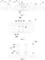
FIG. 1 is a first structural view of a splicing display device according to one embodiment of the present disclosure. -
FIG. 2 is an enlarged view of part H inFIG. 1 . -
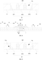
FIG. 3 is a first structural view of a fastening module of the splicing display device according to one embodiment of the present disclosure. -
FIG. 4 is a second structural view of the fastening module of the splicing display device according to one embodiment of the present disclosure. -
FIG. 5 is a third structural view of the fastening module of the splicing display device according to one embodiment of the present disclosure. -
FIG. 6 is a second structural view of the splicing display device according to one embodiment of the present disclosure. -
FIG. 7 is an enlarged view of part K inFIG. 6 . -
FIG. 8 is a third structural view of the splicing display device according to one embodiment of the present disclosure. -
FIG. 9 is an enlarged view of part L inFIG. 6 . -
FIG. 10 is a fourth structural view of the splicing display device according to one embodiment of the present disclosure. - The technical solutions in the present disclosure will be clearly and completely described below in conjunction with accompanying drawings and with reference to specific embodiments. Obviously, the embodiments are only some of the embodiments of the present disclosure, rather than all the embodiments. Based on the embodiments in the present disclosure, all other embodiments obtained by those skilled in the art without creative work shall fall within the protection scope of the present disclosure. In addition, it should be understood that the specific embodiments described here are only used to illustrate and explain the present disclosure, and are not used to limit the present disclosure. In the present disclosure, unless otherwise specified, directional terms such as "upper" and "lower" generally refer to the upper and lower directions of a device in actual use or work state, and specifically refer to the directions in the drawings. The terms "inner" and "outer" are referred to with reference to outlines of the device.
- The present disclosure provides a splicing display device. Detailed descriptions are provided below. It should be noted that an order of descriptions in the following embodiments is not intended to limit a preferred order of the embodiments.
- Referring to
FIGs. 1 and 2 , an embodiment of the present disclosure provides asplicing display device 1000. Thesplicing display device 1000 includes at least twodisplay devices 100, a plurality of light-emitting diode (LED)substrates 200 and a plurality offastening modules 300. - At least two
display devices 100 are spliced to form a plurality of gaps Fx. Eachdisplay device 100 includes asupport module 11 and apanel 12 arranged on thesupport module 11. - Each
LED substrate 200 is arranged on twoadjacent display devices 100. EachLED substrate 200 covers one of the gaps Fx. TheLED substrate 200 includes abase 21, a plurality of LED elements, and a plurality of firstmagnetic members 23. Thebase 21 is arranged on twoadjacent panels 12. TheLED elements 22 are arranged on thebase 21, and the firstmagnetic members 23 are arranged on one side of the base 21 away from theLED elements 22. - Each
fastening module 300 includes afastening element 31 and a plurality ofmagnetic assemblies 32. Thefastening elements 31 are arranged on thesupport modules 11. At least a portion of eachfastening element 31 is arranged corresponding to one of the gaps Fx. The magnetic assemblies are arranged on thefastening elements 31 and located in the plurality of gaps Fx. Themagnetic assemblies 32 are magnetically connected to the firstmagnetic members 23. - The
splicing display device 1000 of the present disclosure uses thefastening modules 300 and the firstmagnetic members 23 arranged on theLED substrates 200 to achieve magnetic attraction connection, which simplifies installation of theLED substrates 200 and enhances adjustability of theLED substrates 200. - Optionally, in the
display device 100, thesupport module 11 is a backlight module, and thepanel 12 is a liquid crystal panel. The present embodiment combines liquid crystal display devices and theLED substrates 200, thus reducing costs of thesplicing display device 1000. - Optionally, in some embodiments, each
support module 11 includes a backplate. Thepanels 12 are non-liquid-crystal panels, thepanels 12 are arranged on the backplates, and eachfastening elements 31 are arranged on one sides of the backplates away from thepanels 12. - For example, the non-liquid crystal panel can be a sub-millimeter light emitting diode (Mini-LED) panel, a micro light emitting diode (Micro-LED) panel, an organic light emitting diode (OLED) panel, or a quantum dot light emitting diode (QLED) panel.
- Optionally, the first
magnetic member 23 includes material selected from one of a magnetic conductor material or a permanent magnetic material. For example, the material can be iron, silicon steel, iron-aluminum alloy, permalloy, sendust alloy, spinel-type ferrites, and planar hexagonal ferrites. The material can also be magnetic steel, metal permanent magnet, magnetoplumbite type ferrites, and rare earth permanent magnet materials. - Optionally,
redundant bond pads 24 are disposed on thebase 21. Theredundant bond pads 24 are disposed on one side of the base 21 away from theLED elements 22. The firstmagnetic member 23 is fixedly connected to theredundant bond pad 24. - The first
magnetic members 23 are fixed on theredundant bond pads 24. On the one hand, idle bond pads are reasonably used. On the other hand, the welding method is used to achieve stable connection between the firstmagnetic members 23 and theredundant bond pads 24. - In some embodiments, the first
magnetic member 23 can also be a coating on theredundant bond pad 24. That is to say, the firstmagnetic member 23 is a film layer doped with magnetic particles. - Optionally, the
redundant bond pads 24 can be made of a conductive material such as metal or metal oxide. In the present embodiment, theredundant bond pads 24 can be made of metal. - Optionally, one end of the
fastening element 31 is connected to the back of onesupport module 11, and another end of thefastening element 31 is connected to the back of anothersupport module 11. Thefastening element 31 crosses the gap Fx. Themagnetic assembly 32 is disposed on a portion of thefastening element 31 corresponding to the gap Fx. - The
fastening element 31 is fixed to the backs of thesupport modules 11 of twoadjacent display devices 100, thereby improving the stability and convenience in assembling thefastening module 300 and thedisplay devices 100. - Optionally, the
panel 12 includes a display area AA and a non-display area NA, and the non-display area NA is arranged outside the display area AA. - The
LED substrate 200 is correspondingly disposed on the non-display area NA of thepanel 12. - Optionally, referring to
FIG. 3 , themagnetic assembly 32 includes a supportingbase 321, a connectingelement 322 and a secondmagnetic member 323. The supportingbase 321 is disposed on thefastening member 31. The connectingelement 322 is extendably arranged on the supportingbase 321. The secondmagnetic member 323 is disposed on the connectingelement 322. - The connecting
element 322 is extendably arranged on the supportingbase 321, and therefore the present disclosure can easily adjust a vertical position of theLED substrate 200, and improves the stability and applicability in installing theLED substrate 200. - Optionally, each supporting
base 321 is provided with a threadedhole 32a, an outer surface of each connectingelement 322 is provided with a plurality of threads, and the connectingelements 322 are threadedly connected to the threadedholes 32a. - In the present embodiment, the connecting
element 322 is extendable by means of a threaded connection, and the threaded connection achieves precise extendable functions and a convenient telescopic extension of the connectingelement 322. - Optionally, the second
magnetic member 323 includes material selected from one of a magnetic conductor material or a permanent magnetic material. For example, the material can be iron, silicon steel, iron-aluminum alloy, permalloy, sendust alloy, spinel-type ferrites, and planar hexagonal ferrites. The material can also be magnetic steel, metal permanent magnet, magnetoplumbite type ferrites, and rare earth permanent magnet materials. - At least one of the first
magnetic member 23 or the secondmagnetic member 323 is a permanent magnetic member. - Optionally, please refer to
FIG. 4 for alternative embodiments. Compared with the embodiment ofFIG. 3 , the present embodiment can also adopt an engagement connection method to realize the telescopic extension of the connectingelement 322. - In detail, the present embodiment is different from the embodiment of
FIG. 3 in that, in themagnetic assembly 32, a connectinghole 32b is defined in one side of the supportingbase 321 facing theLED substrate 200. An inner surface of the connectinghole 32b is provided with one ofengagement blocks 32c orengagement grooves 32d arranged at intervals, and the outer surface of the connectingmember 322 is provided with the other of the engagement blocks 32c or theengagement grooves 32d. The connectingelement 322 is disposed in the connectinghole 32b. The engagement blocks 32c and theengagement grooves 32d are engaged with each other. - The engagement blocks 32c and the
engagement grooves 32d are arranged at intervals along a telescopic direction of the connectingelement 322. - The present embodiment is illustrated using an example in which the
engagement grooves 32d are defined in the inner surface of the connectinghole 32b, and the connectingelement 322 includes the engagement blocks 32c; however, the present disclosure is not limited in this regard. - Optionally, a plurality of guiding
grooves 32f are defined in themagnetic assembly 32. The engagement blocks 32c can slide in the guidinggrooves 32f. In the telescopic direction of the connectingelement 322, the guidinggrooves 32f and theengagement grooves 32d are alternately arranged and communicated with each other. A width of the guidinggroove 32f is less than a width of theengagement groove 32d, and a depth of the guidinggroove 32f is less than a depth of theengagement groove 32d. Such configuration facilitates movement of the connectingelement 322 in the connectinghole 32b. - Optionally, please refer to
FIG. 5 for alternative embodiments. The present embodiment is different from the embodiment ofFIG. 3 orFIG. 4 in that the connectingelement 322 and the secondmagnetic member 323 are integrally formed. The connectingelement 322 is a magnetic material. That is to say, the connectingelement 322 and the secondmagnetic member 323 are made of the same material. Such configuration simplifies a structure of themagnetic assembly 32 and improves the stability of the overall structure. - It should be noted that the present embodiment is described by comparing the embodiment of 3 as an example; however, the present disclosure is not limited in this regard.
- Optionally, please refer to
FIG. 6 andFIG. 7 for alternative embodiments. Compared with the foregoing embodiments, the present embodiment is different from the foregoing embodiments in that thefastening element 31 is disposed in the gap Fx. One end of thefastening element 31 is connected to a side surface of onesupport module 11, and another end of thefastening element 31 is connected to a side surface of anothersupport module 11. - The
fastening element 31 is fixed to the side surfaces of thesupport modules 11 of twoadjacent display devices 100 and is located in the gap Fx. As a result, the present disclosure improves the stability of an assembled structure of thefastening module 300 and thedisplay device 100 and saves installation space. - Optionally, the
fastening element 31 includes afirst fastening portion 311, amiddle portion 312, and asecond fastening portion 313. Thefirst fastening portion 311 is fixedly connected to the side surface of onesupport module 11, and thesecond fastening portion 313 is fixedly connected to the side surface of anothersupport module 11. Themiddle portion 312 is connected between thefirst fastening portion 311 and thesecond fastening portion 313. The supportingbase 321 is disposed on themiddle portion 312. - Optionally, please refer to
FIG. 8 and FIG. 9 for alternative embodiments. The present embodiment is different from the embodiment ofFIG. 6 in that, a side of eachsupport module 11 is provided with aninsertion slot 11c, thefirst fastening part 311 is inserted into theinsertion slot 11c of onesupport module 11, and thesecond fastening part 313 is inserted into theinsertion slot 11c of anothersupport module 11. Such configuration facilitates the installation of thefastening module 300. - Optionally, please refer to
FIG. 10 for alternative embodiments. Compared with the foregoing embodiments, thefastening element 31 includes afirst fastening part 31a and asecond fastening part 31b. Themagnetic assemblies 32 include a first magnetic assembly 32m and a second magnetic assembly 32n. - Between two
adjacent display devices 100, thefirst fastening part 31a is arranged on a back or a side surface of onesupport module 11, and thesecond fastening part 31b is arranged on a back or a side surface of anothersupport module 11. The first magnetic assembly 32m is disposed on thefirst fastening part 31a. The second magnetic assembly 32n is disposed on thesecond fastening part 31b. - One
fastening element 31 is installed corresponding to one connecting element, so difficulty of maintenance is reduced. - It should be noted that, the present embodiment is illustrated taking an example in which the
first fastening part 31a and thesecond fastening part 31b are respectively disposed on the back surfaces of thecorresponding support modules 11; however, the present disclosure is not limited in this regard. - Optionally, there is an interval Jx between the
first fastening part 31a and thesecond fastening part 31b. The interval is used for insertion of a flexible circuit board electrically connected to theLED substrate 200. - The splicing display device of the present disclosure includes at least two display devices, a plurality of LED substrates, and a plurality of fastening modules. A plurality of gaps are defined between the at least two display devices, and each display device includes a support module and a panel disposed on the support module. Each LED substrate is arranged on two adjacent display devices and covers one of the gaps. The LED substrate includes a base, a plurality of LED elements and a plurality of first magnetic members, the LED elements are arranged on the base, and the first magnetic members are arranged on one side of the base away from the LED elements. Each fastening module includes a fastening element and a plurality of magnetic assemblies, the fastening elements are arranged on the support modules, at least a portion of each fastening element is arranged corresponding to one of the gaps, the magnetic assemblies are arranged on the fastening elements and located in the plurality of gaps, and the magnetic assemblies are magnetically connected to the first magnetic members.
- The present disclosure uses the fastening modules and the first magnetic members arranged on the LED substrates to achieve magnetic attraction connection, which simplifies installation of the LED substrates and enhances adjustability of the LED substrates.
- The above is a detailed description to the splicing display device of the present disclosure. Specific examples are used in the present disclosure to illustrate working principles and embodiments of the present disclosure. The descriptions of the above embodiments are only used for ease of understanding the present disclosure. Those skilled in the art can modify the embodiments and the disclosure range according to the ideas of the present disclosure. In conclusion, the contents of the specification should not be construed as a limitation to the present disclosure.
Claims (20)
- A splicing display device, characterized by comprising:at least two display devices, wherein a plurality of gaps are defined between the at least two display devices, and each of the at least two display devices comprises a support module and a panel disposed on the support module;a plurality of light-emitting diode, LED, substrates, wherein each of the LED substrates is arranged on two adjacent ones of the at least two display devices and covers one of the gaps,each of the LED substrates comprises a base, a plurality of LED elements and a plurality of first magnetic members, the base is arranged on two adjacent panels, the LED elements are arranged on the base, and the first magnetic members are arranged on one side of the base away from the LED elements; anda plurality of fastening modules, wherein each of the fastening modules comprises a fastening element and a plurality of magnetic assemblies, fastening elements of the fastening modules are arranged on support modules of the at least two display devices, at least a portion of each of the fastening elements is arranged corresponding to one of the gaps, the magnetic assemblies are arranged on the fastening element and located in one of the gaps, and the magnetic assemblies are magnetically connected to the first magnetic members;a plurality of redundant bond pads are arranged on each base of the LED substrates, the redundant bond pads are arranged on one side of each base away from corresponding LED elements, and the first magnetic members are fixedly connected to the redundant bond pads; andeach of the first magnetic members comprises a material selected from one of a magnetic conductor material or a permanent magnetic material.
- The splicing display device according to claim 1, characterized in that each of the magnetic assemblies comprises a supporting base, a connecting element, and a second magnetic member, supporting bases of the magnetic assemblies are arranged on the fastening elements, connecting elements of the magnetic assemblies are extendably arranged on the supporting bases, and second magnetic members of the magnetic assemblies are arranged on the connecting elements.
- The splicing display device according to claim 2, characterized in that each of the connecting elements and a corresponding second magnetic member of the second magnetic members are integrally formed, and each of the connecting elements is made of a magnetic material.
- The splicing display device according to claim 2, characterized in that each of the supporting bases is provided with a threaded hole, an outer surface of each of the connecting elements is provided with a plurality of threads, and the connecting elements are threadedly connected to threaded holes of the supporting bases.
- The splicing display device according to claim 2, characterized in that one end of each of the fastening elements is connected to a back of one of the support modules, and another end of each of the fastening elements is connected to a back of another one of the support modules, and each of the fastening elements crosses a corresponding gap of the gaps; and each of the connecting elements is arranged on a portion of one of the fastening elements corresponding to one of the gaps.
- The splicing display device according to claim 2, characterized in that each of the fastening elements is disposed in one of the gaps, one end of each of the fastening elements is connected to a side surface of one of the support modules, and another end of each of the fastening elements is connected to a side surface of another one of the support module.
- The splicing display device according to claim 2, characterized in that each of the fastening elements comprises a first fastening part and a second fastening part, and each of the connecting elements comprises a first connecting part and a second connecting part, between two adjacent ones of the at least two display devices, the first fastening part is arranged on a back or a side surface of one of the support modules, and the second fastening part is arranged on a back or a side surface of another one of the support modules, the first connecting part is arranged on the first fastening part, and the second connecting part is arranged on the second fastening part.
- The splicing display device according to claim 1, characterized in that the support modules are backlight modules, and panels of the at least two display devices are liquid crystal panels.
- The splicing display device according to claim 1, characterized in that each of the support modules comprises a backplate, panels of the at least two display devices are non-liquid-crystal panels, the panels are arranged on backplates of the support modules, and the fastening elements are arranged on sides of the backplates away from the panels.
- A splicing display device, characterized by comprising:at least two display devices, wherein a plurality of gaps are defined between the at least two display devices, and each of the at least two display devices comprises a support module and a panel disposed on the support module;a plurality of light-emitting diode, LED, substrates, wherein each of the LED substrates is arranged on two adjacent ones of the at least two display devices and covers one of the gaps, each of the LED substrates comprises a base, a plurality of LED elements and a plurality of first magnetic members, the base is arranged on two adjacent panels, the LED elements are arranged on the base, and the first magnetic members are arranged on one side of the base away from the LED elements; anda plurality of fastening modules, wherein each of the fastening modules comprises a fastening element and a plurality of magnetic assemblies, fastening elements of the fastening modules are arranged on support modules of the at least two display devices, at least a portion of each of the fastening elements is arranged corresponding to one of the gaps, the magnetic assemblies are arranged on the fastening element and located in one of the gaps, and the magnetic assemblies are magnetically connected to the first magnetic members.
- The splicing display device according to claim 10, characterized in that a plurality of redundant bond pads are arranged on each base of the LED substrates, the redundant bond pads are arranged on one side of each base away from the corresponding LED elements, and the first magnetic members are fixedly connected to the redundant bond pads.
- The splicing display device according to claim 10, characterized in that each of the magnetic assemblies comprises a supporting base, a connecting element, and a second magnetic member, supporting bases of the magnetic assemblies are arranged on the fastening elements, connecting elements of the magnetic assemblies are extendably arranged on the supporting bases, and second magnetic members of the magnetic assemblies are arranged on the connecting elements.
- The splicing display device according to claim 12, characterized in that each of the connecting elements and a corresponding second magnetic member of the second magnetic members are integrally formed, and each of the connecting elements is made of a magnetic material.
- The splicing display device according to claim 13, characterized in that each of the supporting bases is provided with a threaded hole, an outer surface of each of the connecting elements is provided with a plurality of threads, and the connecting elements are threadedly connected to threaded holes of the supporting bases.
- The splicing display device according to claim 12, characterized in that one end of each of the fastening elements is connected to a back of one of the support modules, and another end of each of the fastening elements is connected to a back of another one of the support modules, and each of the fastening elements crosses a corresponding gap of the gaps; and each of the connecting elements is arranged on a portion of one of the fastening elements corresponding to one of the gaps.
- The splicing display device according to claim 12, characterized in that each of the fastening elements is disposed in one of the gaps, one end of each of the fastening elements is connected to a side surface of one of the support modules, and another end of each of the fastening elements is connected to a side surface of another one of the support modules.
- The splicing display device according to claim 12, characterized in that each of the fastening elements comprises a first fastening part and a second fastening part, and each of the connecting elements comprises a first connecting part and a second connecting part, between two adjacent ones of the at least two display devices, the first fastening part is arranged on a back or a side surface of one of the support modules, and the second fastening part is arranged on a back or a side surface of another one of the support modules, the first connecting part is arranged on the first fastening part, and the second connecting part is arranged on the second fastening part.
- The splicing display device according to claim 10, the support modules are backlight modules, and panels of the at least two display devices are liquid crystal panels.
- The splicing display device according to claim 10, characterized in that each of the support modules comprises a backplate, panels of the at least two display devices are non-liquid-crystal panels, the panels are arranged on backplates of the support modules, and the fastening elements are arranged on sides of the backplates away from the panels.
- The splicing display device according to claim 10, characterized in that each of the first magnetic members comprises a material selected from one of a magnetic conductor material or a permanent magnetic material.
Applications Claiming Priority (2)
| Application Number | Priority Date | Filing Date | Title |
|---|---|---|---|
| CN202111477605.6A CN114141154B (en) | 2021-12-06 | 2021-12-06 | Spliced display device |
| PCT/CN2021/139939 WO2023103080A1 (en) | 2021-12-06 | 2021-12-21 | Tiled display device |
Publications (2)
| Publication Number | Publication Date |
|---|---|
| EP4447028A1 true EP4447028A1 (en) | 2024-10-16 |
| EP4447028A4 EP4447028A4 (en) | 2026-01-21 |
Family
ID=86608541
Family Applications (1)
| Application Number | Title | Priority Date | Filing Date |
|---|---|---|---|
| EP21966992.6A Pending EP4447028A4 (en) | 2021-12-06 | 2021-12-21 | Tiled display device |
Country Status (3)
| Country | Link |
|---|---|
| US (1) | US11841569B2 (en) |
| EP (1) | EP4447028A4 (en) |
| CN (1) | CN117616490A (en) |
Families Citing this family (3)
| Publication number | Priority date | Publication date | Assignee | Title |
|---|---|---|---|---|
| KR102404360B1 (en) * | 2020-10-23 | 2022-06-02 | 엘지전자 주식회사 | Display control module and display device including same |
| WO2024044945A1 (en) * | 2022-08-30 | 2024-03-07 | 京东方科技集团股份有限公司 | Assembly member for display module, display module, and tiled display device |
| CN118692318A (en) * | 2023-03-21 | 2024-09-24 | 广州华星光电半导体显示技术有限公司 | Splicing display device |
Family Cites Families (27)
| Publication number | Priority date | Publication date | Assignee | Title |
|---|---|---|---|---|
| JP2007192977A (en) | 2006-01-18 | 2007-08-02 | Seiko Epson Corp | Tiling display |
| CN103901643B (en) | 2014-03-20 | 2016-04-13 | 京东方科技集团股份有限公司 | A kind of display screen and mosaic display screen |
| CN105044964A (en) * | 2014-04-01 | 2015-11-11 | 台湾巴可科技股份有限公司 | Spliced display device |
| CN204590355U (en) * | 2015-05-11 | 2015-08-26 | 中亿丰建设集团股份有限公司 | LED flood lighting and curtain wall integral system |
| WO2017011364A1 (en) | 2015-07-10 | 2017-01-19 | Bleich Noah | Tea display and storage device |
| CN105044959B (en) * | 2015-09-14 | 2019-04-05 | 深圳市华星光电技术有限公司 | It is a kind of that seamless spliced multi-display apparatus can be achieved |
| JP2017152553A (en) | 2016-02-25 | 2017-08-31 | セイコーエプソン株式会社 | Electronic component storage container and method of manufacturing electronic component storage container |
| GB201620544D0 (en) * | 2016-12-02 | 2017-01-18 | Barco Nv | Front maintenance apparatus for flexible tiled LED display |
| KR102740814B1 (en) * | 2016-12-20 | 2024-12-09 | 엘지디스플레이 주식회사 | Display apparatus and multi screen display apparatus comprising the same |
| CN106842711A (en) * | 2017-03-29 | 2017-06-13 | 韩玉君 | Display structure and integrated morphology for eliminating FPD platen edge piece |
| WO2020040616A1 (en) * | 2018-08-24 | 2020-02-27 | Samsung Electronics Co., Ltd. | Display apparatus |
| CN112309268A (en) | 2019-07-31 | 2021-02-02 | 海信视像科技股份有限公司 | A display device and a method for manufacturing the same |
| CN210535225U (en) | 2019-09-18 | 2020-05-15 | 广东德豪锐拓显示技术有限公司 | LED display screen |
| CN210720954U (en) | 2019-10-21 | 2020-06-09 | 南京中电熊猫平板显示科技有限公司 | Backlight module |
| CN210627782U (en) | 2019-12-27 | 2020-05-26 | 深圳市科彤科技有限公司 | Liquid crystal curtain wall convenient to clean |
| CN111276058B (en) | 2020-02-11 | 2022-10-11 | 京东方科技集团股份有限公司 | Splicing display panel and splicing display device |
| CN111312087B (en) | 2020-04-01 | 2021-11-02 | 深圳市华星光电半导体显示技术有限公司 | Splicing screen connecting structure and display device |
| CN111653207B (en) | 2020-07-30 | 2022-12-13 | 上海天马微电子有限公司 | Display module assembly, display device and spliced screen |
| CN114093248A (en) * | 2020-07-31 | 2022-02-25 | 京东方科技集团股份有限公司 | Tiled display unit, tiled display device and manufacturing method thereof |
| CN111883005A (en) | 2020-08-05 | 2020-11-03 | 张明晓 | Novel LED display screen unit board magnetic pole that stretches out and draws back |
| CN214042924U (en) | 2020-12-24 | 2021-08-24 | 北京京东方光电科技有限公司 | A mounting structure and concatenation screen for splicing screen |
| CN213990829U (en) | 2021-01-29 | 2021-08-17 | 深圳市青象信息科技有限公司 | Multi-screen splicing mixed seamless matrix |
| CN112863390B (en) | 2021-03-09 | 2023-02-28 | 上海中航光电子有限公司 | Light-emitting module, backlight module and display device |
| CN214669956U (en) * | 2021-04-28 | 2021-11-09 | 惠州视维新技术有限公司 | Seamless splicing display |
| CN113516923B (en) * | 2021-07-29 | 2022-10-04 | Tcl华星光电技术有限公司 | Display screen splicing device and splicing display device |
| CN113703211B (en) | 2021-08-16 | 2023-02-03 | Tcl华星光电技术有限公司 | Tiled display device |
| US11914240B2 (en) * | 2021-12-27 | 2024-02-27 | Tcl China Star Optoelectronics Technology Co., Ltd. | Spliced display screen |
-
2021
- 2021-12-21 EP EP21966992.6A patent/EP4447028A4/en active Pending
- 2021-12-21 CN CN202180099875.XA patent/CN117616490A/en active Pending
- 2021-12-21 US US17/597,229 patent/US11841569B2/en active Active
Also Published As
| Publication number | Publication date |
|---|---|
| CN117616490A (en) | 2024-02-27 |
| US20230176411A1 (en) | 2023-06-08 |
| EP4447028A4 (en) | 2026-01-21 |
| US11841569B2 (en) | 2023-12-12 |
Similar Documents
| Publication | Publication Date | Title |
|---|---|---|
| CN116486708B (en) | splicing display device | |
| US11841569B2 (en) | Splicing display device | |
| US12094372B2 (en) | Display device | |
| EP3667405B1 (en) | Backlight unit and liquid crystal display including the same | |
| US7864516B2 (en) | Display unit and multi-display device having the same | |
| KR102807721B1 (en) | Display device and tiling display device | |
| US12360413B2 (en) | Splicing display panel and electronic device | |
| CN113748372B (en) | Bar display structure, display panel and display device | |
| CN114299828B (en) | Display unit, spliced screen and display device | |
| CN114415410A (en) | Splicing display module and display device | |
| CN219609938U (en) | Spliced display device | |
| CN211698505U (en) | display device | |
| KR102847144B1 (en) | Display device | |
| EP4167280A1 (en) | Display device comprising semiconductor light-emitting element | |
| KR102843566B1 (en) | Display device | |
| CN119360748B (en) | Display modules, display devices, adjustment devices and methods, splicing display equipment | |
| US20260020396A1 (en) | Display device | |
| KR20250080222A (en) | Display device including semiconductor light emitting device | |
| CN117518604A (en) | Light-emitting substrate and display device | |
| KR20250051204A (en) | Display device | |
| KR20250115036A (en) | A semiconductor lightemitting device package for display pixels, assembly substrate including the same, and assembly method thereof | |
| CN121191395A (en) | splicing display panels and display devices | |
| KR20220086120A (en) | Display device and tiling display device | |
| KR20220026073A (en) | Display Device |
Legal Events
| Date | Code | Title | Description |
|---|---|---|---|
| STAA | Information on the status of an ep patent application or granted ep patent |
Free format text: STATUS: THE INTERNATIONAL PUBLICATION HAS BEEN MADE |
|
| PUAI | Public reference made under article 153(3) epc to a published international application that has entered the european phase |
Free format text: ORIGINAL CODE: 0009012 |
|
| STAA | Information on the status of an ep patent application or granted ep patent |
Free format text: STATUS: REQUEST FOR EXAMINATION WAS MADE |
|
| 17P | Request for examination filed |
Effective date: 20240209 |
|
| AK | Designated contracting states |
Kind code of ref document: A1 Designated state(s): AL AT BE BG CH CY CZ DE DK EE ES FI FR GB GR HR HU IE IS IT LI LT LU LV MC MK MT NL NO PL PT RO RS SE SI SK SM TR |
|
| DAV | Request for validation of the european patent (deleted) | ||
| DAX | Request for extension of the european patent (deleted) | ||
| A4 | Supplementary search report drawn up and despatched |
Effective date: 20251218 |
|
| RIC1 | Information provided on ipc code assigned before grant |
Ipc: G09F 9/302 20060101AFI20251212BHEP Ipc: H04N 5/65 20060101ALI20251212BHEP Ipc: H05K 5/00 20060101ALI20251212BHEP |