EP4446786A1 - Optical element, light source module, and display device - Google Patents
Optical element, light source module, and display device Download PDFInfo
- Publication number
- EP4446786A1 EP4446786A1 EP21966719.3A EP21966719A EP4446786A1 EP 4446786 A1 EP4446786 A1 EP 4446786A1 EP 21966719 A EP21966719 A EP 21966719A EP 4446786 A1 EP4446786 A1 EP 4446786A1
- Authority
- EP
- European Patent Office
- Prior art keywords
- light
- light source
- ring
- center
- optical component
- Prior art date
- Legal status (The legal status is an assumption and is not a legal conclusion. Google has not performed a legal analysis and makes no representation as to the accuracy of the status listed.)
- Granted
Links
Images




Classifications
-
- F—MECHANICAL ENGINEERING; LIGHTING; HEATING; WEAPONS; BLASTING
- F21—LIGHTING
- F21V—FUNCTIONAL FEATURES OR DETAILS OF LIGHTING DEVICES OR SYSTEMS THEREOF; STRUCTURAL COMBINATIONS OF LIGHTING DEVICES WITH OTHER ARTICLES, NOT OTHERWISE PROVIDED FOR
- F21V9/00—Elements for modifying spectral properties, polarisation or intensity of the light emitted, e.g. filters
- F21V9/40—Elements for modifying spectral properties, polarisation or intensity of the light emitted, e.g. filters with provision for controlling spectral properties, e.g. colour, or intensity
-
- G—PHYSICS
- G02—OPTICS
- G02B—OPTICAL ELEMENTS, SYSTEMS OR APPARATUS
- G02B5/00—Optical elements other than lenses
- G02B5/18—Diffraction gratings
- G02B5/1809—Diffraction gratings with pitch less than or comparable to the wavelength
-
- G—PHYSICS
- G02—OPTICS
- G02B—OPTICAL ELEMENTS, SYSTEMS OR APPARATUS
- G02B5/00—Optical elements other than lenses
- G02B5/18—Diffraction gratings
- G02B5/1866—Transmission gratings characterised by their structure, e.g. step profile, contours of substrate or grooves, pitch variations, materials
- G02B5/1871—Transmissive phase gratings
Definitions
- the present disclosure relates to an optical component, a light source module and a display device. More particular, the present disclosure relates to the optical component which emits the light uniformly, and also relates to the light source module and the display device including this optical component.
- LEDs light emitting diodes
- Those display devices are usually equipped with at least one component for light uniformity, for example, with a diffuser to uniform the light, and thus the light from the LEDs may be emitted uniformly.
- numbers of producers dedicate their effort to researching and improving the component for light-uniformity with distinctive optical principles in order to achieve the uniformity of emitting light, and further to improve the image quality of the display devices.
- an object for the disclosure is to provide an optical component, and its light incident surface and the light exiting surface can use the effect of near-field diffraction and thus,achieve the uniformity of emitting light.
- At least one embodiment of the disclosure provides an optical component.
- the optical component uniforms the light through the effect of near-field diffraction.
- At least one embodiment of the disclosure provides a light source module including the optical component.
- At least one embodiment of the disclosure provides a display device including the light source module.
- At least one embodiment of the disclosure provides an optical component.
- the optical component has a light incident surface and a light exiting surface opposite to the light incident surface. At least one light source is suitable for emitting light toward the light incident surface.
- the optical component includes at least one phase diffraction grating and at least one amplitude diffraction grating.
- the phase diffraction grating includes a center concave section and a plurality of ring stages surrounding the center concave section and arranged in concentric circles. The center concave section and the plurality of ring stages are formed to be the light incident surface defining a cavity and becoming an inner surface of the cavity.
- Each of the ring stages has a first stage surface, and each of the first stage surfaces includes a plurality of ring microstructures arranged in concentric circles.
- a width of each of the ring microstructures on at least one of the ring stages is less than or equal to a quarter of a wavelength of the light.
- the amplitude diffraction grating includes a center convex section aligned to the center concave section, and includes a plurality of ring parts surrounding the center convex section and arranged in concentric circles. The center convex section and the ring parts are formed to be the light exiting surface.
- the amplitude diffraction grating perpendicularly projects a projective region on the light incident surface, and the phase diffraction grating entirely overlaps the projective region.
- the width of each of the ring parts is less than or equal to the wavelength of the light.
- the light source has a top surface
- the ring stages above the top surface of the light source belong to a first group.
- a plurality of first angles are each formed between the top surface of the light source and the first stage surface of each of the ring stages in the first group. These first angles of the first group increasingly decrease in a direction away from the center concave section.
- the ring stages below the top surface of the light source belong to a second group.
- a plurality of second angles are each formed between the top surface of the light source and the first stage surface of each of the ring stages in the second group. These second angles of the second group increasingly increase in a direction away from the center concave section.
- the center convex section and the ring parts form a depression.
- the optical component further has a surface.
- the light incident surface is concavely disposed on the surface, and the light exiting surface is opposite to the surface.
- Each of the ring parts has a second stage surface, and each of a plurality of vertical distances between the second stage surface of each of the ring parts and the surface decrease in a direction away from the center convex section.
- the widths of theses ring stages are equal to each other.
- the widths of theses ring microstructures in the same first stage surface are equal to each other.
- the widths of these ring parts are equal to each other.
- the vertical distance between the bottom surface of the center concave section and the top surface of the light source is less than 4 mm.
- the optical component further includes a light incident layer, a light exiting layer and a center layer.
- the light incident layer has a light incident surface, and the at least one phase diffraction grating is concavely disposed on the light incident surface.
- the light exiting layer has a light exiting surface, and the at least one amplitude diffraction grating is formed in the light exiting surface.
- the center layer is disposed between the light incident layer and the light exiting layer.
- the refractive index of the center layer is less than the refractive index of the light incident layer or the refractive index of the light exiting layer.
- the disclosure provides a light source module including the optical component and light-emitting assembly.
- the light-emitting assembly includes at least one light source which is disposed in the cavity defined by the light incident surface.
- the light source is a monochromatic light source.
- the wavelength of the light from the light source is between 400 nm and 500 nm, and the widths of each of the ring microstructures are between 100 nm and 125 nm.
- the light source has an optical axis.
- the center convex section and the center concave section aligned to each other are coaxial.
- a center axis of the center concave section overlaps the optical axis.
- Another embodiment of the disclosure provides a display device including a light source module and a display panel which is disposed opposite to the light source module.
- the width of each ring microstructures on at least one ring stage is less than or equal to a quarter of wavelength of the light from the light source, hence, the phase diffraction grating is able to generate the near-field diffraction of the light to disperse the light.
- the amplitude diffraction grating is able to collimate the dispersed light in order to emit the light uniformly, and make the light source module appropriate to be applied on display devices, so that the image quality is improved.
- the dimensions (such as lengths, widths and thicknesses) of components (such as layers, films, substrates and regions) in the drawings are enlarged not-to-scale, and the number of components may be reduced in order to clarify the technical features of the disclosure. Therefore, the following illustrations and explanations are not limited to the number of components, the number of components, the dimensions and the shapes of components, and the deviation of size and shape caused by the practical procedures or tolerances are included.
- a flat surface shown in drawings may have rough and/or non-linear features, while angles shown in drawings may be circular.
- the drawings of components shown in the disclosure are mainly for illustration and not intended to accurately depict the real shapes of the components, nor are intended to limit the scope of the claimed content of the disclosure.
- the disclosure provides an optical component which has a light incident surface and a light exiting surface opposite to the light incident surface, and is able to be applied to at least a light source.
- the aforementioned light source is appropriate for emitting the light toward the light incident surface.
- the optical component includes at least a phase diffraction grating and at least an amplitude diffraction grating, in which the light source uses Raman-Nath diffraction (e.g. the near-field diffraction) for producing the constructive interference.
- the phase diffraction grating is primary used for generating optical path differences and enhancing diffraction efficiency while the amplitude diffraction grating is used for generating the superposition wave effect of wave optics.
- the phase diffraction grating includes a center concave section and a plurality of ring stages.
- the ring stages surround the center concave section and are arranged in concentric circles.
- the center concave section and the ring stages form the light incident surface.
- the light incident surface defines a cavity.
- the inner surface of this cavity is composed by the center concave section and the ring stages, and each of the ring stages has a first stage surface.
- Each of the first stage surfaces includes a plurality of ring microstructures arranged in concentric circles.
- the amplitude diffraction grating includes a center convex section and a plurality of ring parts, and the center convex section is aligned to the center concave section.
- the ring parts surround the center convex section and are arranged in concentric circles.
- the center convex section and the ring parts form the light exiting surface. Furthermore, when the width of the phase diffraction grating is equivalent to the wavelength of the light source, the effect of the wave optics becomes more significant.
- the optical components of the disclosure is able to receive the light emitted from the light source with the light incident surface formed by the phase diffraction grating, and the phase diffraction grating is able to disperse this light in order to make the partial light enters the optical component through the light incident surface at a larger light emergent angle.
- the light transmitted in the optical component propagates toward the light exiting surface formed by the amplitude diffraction grating, and then exits from the light exiting surface.
- the amplitude diffraction grating is able to collimate the light which is dispersed by the phase diffraction grating in order to achieve the uniformity of emitting light.
- each of the ring microstructures on at least one of the ring stages in the phase diffraction grating is less than or equal to a quarter wavelength of the light from the light source.
- a phase shift can be generated, and the phase diffraction grating is able to generate the near-field diffraction of the light to disperse this light.
- the amplitude diffraction grating is able to collimate the aforementioned scattered light in order to make the light emitted uniformly, and to make the light source module appropriate to be applied on display devices, so that the image quality is improved.
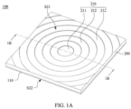
- FIG 1A illustrates a stereoscopic view of a light module in accordance with an embodiment of the present disclosure.
- the light source module 100 includes the light-emitting assembly 110 and the optical component 200.
- the optical component 200 is disposed opposite to the light-emitting assembly 110, and the optical component 200 and the light-emitting assembly 110 are stacked on each other.
- the optical component 200 has the surface S22 adjacent to the light-emitting assembly 110. A portion of the surface S22 may be a plane.
- the optical component 200 includes the amplitude diffraction grating 210 which is opposite to the surface S22.
- the amplitude diffraction grating 210 and the surface S22 are located on the opposite sides of the optical component 200 respectively.
- the amplitude diffraction grating 210 includes the center convex section 211 and the plurality of ring parts 212.
- the ring parts 212 surround the center convex section 211 and are arranged in concentric circles as shown in FIG 1A .
- the light-emitting assembly 110 emits the light toward the optical component 200. Because the whole optical component 200 is transparent, the light emitted from light-emitting assembly 110 passes through the optical component 200 and then exits from the center convex section 211 and the ring parts 212. Therefore, the center convex section 211 and the ring parts 212 is able to form the light exiting surface S21 of the optical component 200, and the light exiting surface S21 is opposite to the surface S22.
- FIG 1B illustrates a cross-sectional view taken along a line 1B-1B of FIG 1A .
- the widths 212w of the ring parts 212 may substantially equal to each other while the width 212w of each of the ring parts 212 is equal to a half of the difference between the outer ring diameter and the inner ring diameter.
- the width 212w is basically equal to the distance between the inner edge (not shown) of the ring parts 212 and the outer edge (not shown) of the ring parts 212.
- the width 212w may be a horizontal width, that is, the width 212w may be the width of the projection of the ring parts 212 projected onto a horizontal direction D1 (namely the half difference between the outer ring diameter and the inner ring diameter). Furthermore, in the embodiment of FIG 1B , the surface S22 may be parallel to the horizontal direction D1, and thus the width 212w may be the width of the projection of ring parts 212 projected onto the surface S22.
- the widths 212w of the ring parts 212 may be slightly different with each other due to the influence of the processing limitations. Hence, the widths 212w may be unequal to each other within an allowable tolerance.
- the center convex section 211 and the ring parts 212 may form a depression in the amplitude diffraction grating 210.
- the light exiting surface S21 on the amplitude diffraction grating 210 may define this depression.
- the inner surface of the depression includes the side wall and the bottom surface. That is, the light exiting surface S21 may be a concave surface.
- the optical component 200 has not only the light exiting surface S21 but a light incident surface 229 opposite to the light exiting surface S21.
- the light incident surface 229 is concavely disposed on the surface S22, and thus the light incident surface 229 may be a concave surface.
- the light incident surface 229 may define a cavity and be the inner surface thereof.
- the inner surface includes the side wall and the bottom surface.
- a portion of the surface S22 except the light incident surface 229 may be a plane because the light incident surface 229 is concavely disposed on the surface S22.
- the light-emitting assembly 110 may include at least one light source light source 111 and a circuit substrate 112, and the circuit substrate 112 may be a printed circuit board or an active device array substrate with control circuit.
- the light source 111 which may be a LED, such as a micro LED or a mini LED may emit the light toward the light incident surface 229.
- the light source 111 is mounted on the circuit substrate 112 and disposed in the cavity defined by the light incident surface 229.
- the light source 111 may be mounted on the circuit substrate 112 by the method of flip chip or wire bonding.
- the surface S22 of the optical component 200, especially the plane part, is advantageous for the attachment and the fixation on the circuit substrate 112.
- the optical component 200 further includes the phase diffraction grating 220, while the phase diffraction grating 220 includes the center concave section 221 and the plurality of ring stages 222.
- the phase diffraction grating 220 is opposite to the amplitude diffraction grating 210, and thus the phase diffraction grating 220 and the amplitude diffraction grating 210 are formed on the two opposite sides of the optical component 200 respectively.
- the amplitude diffraction grating 210 may perpendicularly project a projective region P12 on the light incident surface 229 and the surface S22.
- the projective region P12 is formed by projecting the amplitude diffraction grating 210 on the light incident surface 229 and the surface S22 along with a vertical direction D2.
- the vertical direction D2 is perpendicular to the horizontal direction D1.
- the phase diffraction grating 220 entirely overlaps the projective region P12, and thus the amplitude diffraction grating 210 is overlapping on the phase diffraction grating 220 and exceeds all the edges of the phase diffraction grating 220.
- the area of the amplitude diffraction grating 210 is obviously larger than the area of the phase diffraction grating 220.
- Each of the ring stages 222 has a first stage surface 222a while each of the ring parts 212 has a second stage surface 212b, and the second stage surface 212b is an incline.
- Each of the plurality of vertical distances vertical distances VD2 decrease in the direction which is away from the center convex section 211.
- the vertical distance VD2 is parallel to the vertical direction D2 as shown in FIG 1B , and the vertical distance VD2 may be equal to the thickness of the optical component 200.
- Each of the second stage surface 212b has an inner edge (not shown) and an outer edge (not shown) surrounding the inner edge.
- the inner edge is closer to the center convex section 211 than the outer edge. Since each of the plurality of vertical distances VD2 decrease in the direction which is away from the center convex section 211, the inner edge relative to the surface S22 is higher than the outer edge relative to the surface S22 in one second stage surface 212b as shown in FIG 1B .
- FIG 1C illustrates a locally enlarged view of the light source module shown in FIG 1B
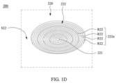
- FIG 1D illustrates a locally stereoscopic view of the optical component on the light incident surface shown in FIG 1A
- the center concave section 221 and the ring stages 222 form the light incident surface 229.
- the ring stages 222 surround the center concave section 221 and are arranged in concentric circles.
- Each first stage surface 222a includes the plurality of ring microstructures R22 arranged in concentric circles, so that each of the ring microstructures R22 also surrounds the center concave section 221.
- the phase diffraction grating 220 may include four ring stages 222, and thus the phase diffraction grating 220 may include even number of the ring stages 222.
- the number of the ring stages 222 which the phase diffraction grating 220 may include is 8 or 16. Therefore, the number of the ring stages 222 is not limited by FIG 1C and FIG 1D .
- each of the first stage surfaces 222a may include four ring microstructures R22 as shown in FIG 1C and FIG 1D .
- these distances between the different ring stages 222 and the circuit substrate 112 are not constant. Take FIG 1C for example, these distances between the ring stages 222 and the circuit substrate 112 increasingly or gradually decrease in the direction which is away from the center concave section 221. Accordingly, the ring stages 222 with larger diameter is closer to the circuit substrate 112 while the ring stages 222 with smaller diameter is farther away from the circuit substrate 112.
- the center convex section 211 is aligned to the center concave section 221, while the aligned center convex section 211 and the center concave section 221 are coaxial, that is, the center axes of center convex section 211 and the center concave section 221 are overlapping.
- the light source 111 has the optical axis A11, while center axes of the center concave section 221 and the center convex section 211 are overlapping with the optical axis A11. Therefore, the optical axis A11 of FIG 1C may be deemed as the center axes of the center concave section 221 and the center convex section 211.
- the widths of the ring stages 222 may be equal to each other substantially, while the widths W22 of the ring microstructures R22 in one first stage surface 222a may be equal to each other substantially.
- the widths W22 of each ring microstructure R22 in each of the ring stages 222 are the same.
- the widths 222w are slightly different with each other, and the widths W22 of one first stage surface 222a are slightly different with each other due to the influence of the processing limitations.
- the widths 222w may be unequal to each other, while the widths W22 may be unequal to each other within an allowable tolerance.
- the light source 111 is able to emit the light L11 toward the light incident surface 229.
- the light source 111 may be a monochromatic light source, so that the light L11 may be a monochromatic light with a narrow spectral linewidth.
- the wavelength of the light L11 emitted from the light source 111 may be between 400 nm and 500 nm.
- the light L11 may be 400 nm or 500 nm.
- the color of the light L11 may be blue-green (the wavelength is about 500 nm), blue or purple (the wavelength is about 400 nm).
- the light L11 may be an invisible light, such as a UV light (the wavelength is about 380 nm).
- the color of the light L11 is not limited by this embodiment, that is, the light L11 may be other visible light.
- the width W22 of each ring microstructure R22 on at least one of the ring stage 222 is less than or equal to a quarter wavelength of the light L11.
- the width W22 of each ring microstructure R22 in each of the ring stages 222 is less than or equal to a quarter wavelength of the light L11.
- the wavelength of the light L11 is between 400 nm and 500 nm
- the widths W22 of each ring microstructure R22 may be between 100 nm and 125 nm.
- the widths W22 may be 100 nm, 125 nm or 110 nm.
- each ring part 212 may be less than or equal to the wavelength of the light L11.
- the light source 111 has the top surface 111t, and the depth D22 which may be the vertical distance between the bottom of the center concave section 221 and the top surface 111t may be less than 4 mm as shown in FIG 1C .
- the cavity design defined by the light incident surface 229 is helpful for reducing the thickness of the light source module 100 and the optical component 200, so that the light source module 100 is on trend of thinning development of present mobile devices (e.g. smartphones and tablets). Additionally, the light L11 of the light source 111 is able to be emitted from the top surface 111t.
- the top surface 111t may be as the light exiting surface of the light source 111.
- the light source 111 is able to be emitted from the side surface and the top surface 111t in order to increase the light emergent angle of the light source 111.
- the optical component 200 may further include a light incident layer 201, a light exiting layer 202 and a center layer 203.
- the center layer 203 is disposed between the light incident layer 201 and the light exiting layer 202.
- the light incident layer 201 has the light incident surface 229, so that the phase diffraction grating 220 is concavely disposed on and formed in the light incident layer 201.
- the light exiting layer 202 has the light exiting surface S21, so that the amplitude diffraction grating 210 is also concavely disposed on and formed in the light exiting layer 202.
- the light incident layer 201 and the light exiting layer 202 may be formed of the same materials.
- the light incident layer 201 and the light exiting layer 202 may be made of the UV curing adhesives, and the refractive indexes of the light incident layer 201 and the light exiting layer 202 are about 1.61.
- the phase diffraction grating 220 and the amplitude diffraction grating 210 may be formed by imprinting or roll-to-roll processing, which imprints the featured patterns on the circumference of the roller over the surfaces of the light incident layer 201 and the light exiting layer 202.
- the center layer 203 may be made of polymer material, which is, for example, polycarbonate (PC), poly methyl methacrylate (PMMA), or methyl methacrylate styrene copolymer (MS).
- PC polycarbonate
- PMMA poly methyl methacrylate
- MS methyl methacrylate styrene copolymer
- the refractive index of the center layer 203 may be between 1.4 and 1.6, such as 1.49, 1.57 or 1.59. Therefore, the refractive index of the center layer 203 may be less than the refractive index of the light incident layer 201 or the light exiting layer 202 (for example, the refractive indexes of the light incident layer 201 and the light exiting layer 202 are about 1.61), so that the light L11 through the interface between the center layer 203 and the light incident layer 201 may be matched with the light incident angle for the near-field diffraction, and thus the amplitude diffraction grating 210 is able to collimate the light dispersed by the phase diffraction grating 220 in order to achieve the light-uniformity.
- FIG 1E illustrates the locally enlarged view of the light module of FIG 1C
- FIG 1E only depicts the left part of the light source module 100 of FIG 1C
- the ring stages 222 are distributed above and beneath the top surface 111t.
- the ring stages 222 above the top surface 111t belong to the first group G11 while the ring stages 222 beneath the top surface 111t belong to the second group G12.
- the ring stages 222 are classified according to the positions of the first stage surfaces 222a relative to the top surface 111t. Specifically, the ring stages 222 with the first stage surface 222a higher than the top surface 111t belong to the first group G11, and the ring stages 222 with the first stage surface 222a lower than the top surface 111t belong to the second group G12.
- First angles A01 are formed between the top surface 111t of the light source 111 and each of the first stage surfaces 222a of the first group G11, while second angles A02 are between the top surface 111t of the light source 111 and each of the first stage surfaces 222a of the second group G12.
- the first angles A01 increasingly or gradually decrease in the direction away from the center concave section 221. Accordingly, the first angle A01 which is the closest to the center concave section 221 is the largest, while the first angle A01 which is the farthest from the center concave section 221 is the smallest.
- the second angles A02 increasingly or gradually increase in the direction which is away from the center concave section 221.
- the second angle A02 which is the closest to the center concave section 221 is the smallest, while the second angle A02 which is the farthest from the center concave section 221 is the largest.
- the feature that the angle between each first stage surface 222a of the ring stages 222 and the optical axis of the light source 111 increases with the increasing diameter of the ring stage, is able to allow the light incident surface 229 of the optical component 200 to receive the light L11 uniformly.
- the phase diffraction grating 220 includes the ring stages 222, and each ring stage 222 includes the ring microstructures R22.
- the widths W22 of each ring microstructure R22 are less than or equal to a quarter of the wavelength of the light L11.
- the phase diffraction grating 220 is able to generate the near-field diffraction of the light L11, and thus the light L11 is dispersed into multiple-order light such as the 0 order, 1st order, 2nd order and 3rd order diffractive light. Accordingly, the phase diffraction grating 220 may disperse the light L11, so that the light L11 is not accumulated in the optical component 200.
- the ring microstructures R22 is able to increase the optical path difference so that the phase diffraction grating 220 disperses the light L11 into multiple lights (as the multiple-order light mentioned above), and thus the diffraction angle is increased to uniform the light L 11.
- the amplitude diffraction grating 210 may collimate the multiple-order light generated by the phase diffraction grating 220, and the light L11 is able to be emitted uniformly from the light exiting surface S21, so that the light source module 100 is advantageously used as the light source of the display devices.
- each optical component 200 of FIG 1A to FIG 1E includes one amplitude diffraction grating 210 and one phase diffraction grating 220, respectively, while each light-emitting assembly 110 includes one light source 111.
- the optical component may include a plurality of amplitude diffraction gratings and a plurality of phase diffraction gratings while the light-emitting assembly may include a plurality of light sources, for example, as a light source module 500 shown in FIG 2A .
- FIG 2A illustrates the bottom view of a light source module in accordance with at least an embodiment of the present disclosure
- FIG 2B illustrates the top view of the light source module of FIG 2A
- the light source module 500 includes the optical component 600 and the light-emitting assembly.
- the light-emitting assembly of the light source module 500 includes the plurality of the light sources 111.
- the light-emitting assembly in the embodiment may further include a circuit substrate (such as the circuit substrate 112 not shown in FIG 2A and FIG 2B ), and the light sources 111 are mounted on the circuit substrate 112.
- the optical component 600 may include the plurality of amplitude diffraction gratings 210 and the plurality of phase diffraction gratings 220.
- the phase diffraction gratings 220 may be arranged in an array (as shown in FIG 2A ) while the amplitude diffraction gratings 210 may be arranged in an array (as shown in FIG 2B ).
- the light sources 111 are disposed in the phase diffraction grating 220 respectively, while the number of the light sources 111 may be equal to the number of the phase diffraction gratings 220.
- the amplitude diffraction gratings 210 are adjacent to each other, and the edges of two adjacent amplitude diffraction gratings 210 may be connected with each other as shown in FIG 2B .
- the amplitude diffraction gratings 210 are aligned to the phase diffraction gratings 220 respectively. Therefore, the center axes of the center convex sections 211 of the amplitude diffraction gratings 210 are substantially overlapping to the center axes of the center convex sections 211 (not shown) of the phase diffraction gratings 220. Moreover, the numbers of the light sources 111, the phase diffraction gratings 220 and the amplitude diffraction gratings 210 may be the same.
- FIG 2C illustrates the cross-section view of a light source module of FIG 2A .
- the light sources 111 of the light source module 500 emit the light
- the light L11 emitted from the light sources 111 enters the phase diffraction gratings 220 and is diffracted by the phase diffraction gratings 220.
- Each light L11 has the plurality of wavefronts W11, and the phase diffraction grating 220 is able to make the wavefronts W11 of the light L11 form a non-plane wave, such as the spherical wave shown in FIG 2C .
- the wavefronts W11 of the lights L11 are superposed to each other, and thus the light L11 of the light sources 111 may interfere with each other.
- the amplitude diffraction gratings 210 can make the wavefronts W11 of the light L11 emitted by the amplitude diffraction gratings 210 turn into a plane wave (as shown in FIG 2C ). Accordingly, the interfered light L11 may be uniformed by the amplitude diffraction gratings 210, so that the light L11 emitted from the light sources 111 may be emitted uniformly from the amplitude diffraction gratings 210.
- the scale of the light source module 500 shown in FIG 2C is different from the scale of the light source module 100 shown in FIG 1B and FIG 1C , and the components of the light source module 500 of FIG 2C (e.g. the amplitude diffraction grating 210 and the phase diffraction grating 220) are not on the same scale, so that the interference phenomenon is clearly to be shown so as to clearly present the technical features of this disclosure.
- the light source module 500 includes the plurality of light sources 111 and the optical component 600, while the optical component 600 includes the plurality of amplitude diffraction gratings 210 and the plurality of phase diffraction gratings 220, so that the light source module 500 is appropriate to be applied on display devices, especially on large scale display devices.
- the light source module 500 is appropriate for large scale display devices and being as the direct type backlight module of the display device.
- the circuit substrate 112 mounted with the light sources 111 may have a control circuit (not shown), which controls the light sources 111 to emit the light.
- the control circuit is able to control the light sources 111 in at least two different regions, and thus these regions may present two different kinds of brightness in order to achieve the dimming effect and improve the contrast.
- FIG 3 illustrates a schematic diagram of a display device in accordance with one embodiment of the present disclosure'.
- the display device 800 includes the light source module 700 and the display panel 810, and the display panel 810 is disposed oppositely to the light source module 700.
- the light source module 700 may be the light source module 100 or the light source module 500 of the aforementioned embodiments, and thus the light source module 700 may include at least one light source 111 and the circuit substrate 112 (are not shown in FIG 3 ).
- the light source module 700 includes the plurality of light sources 111 and the light sources 111 are monochromatic light sources
- the circuit substrate 112 may be a transistor array substrate with a plurality of thin-film transistors (TFTs)
- the display panel 810 may include several kinds of wavelength converting layers (not shown).
- the wavelength converting layers may convert the light L11 emitted from the light source 111 into the light with different colors.
- the light L11 may be blue light
- the wavelength converting layers is able to convert the lights L11 of the light sources 111 into red or green light, so that the display panel 810 is able to present the images consist of red, green and blue light.
- the materials of the wavelength converting layers may be fluorescent materials or quantum dots materials while the display device 800 may be a quantum dots light LED (QLED) display.
- QLED quantum dots light LED
- the optical component of the light source module 700 may include the light incident layer 201, the light exiting layer 202 and the center layer 203, as the light source module 100 shown in FIG 1C . Therefore, the total internal reflection (TIR) occurs inside the optical component of the light source module 700 (namely the interface between the center layer 203 and the light incident layer 201) in order to reflect the light L11 deviated from the optical axis A11, and the light leakage of the display device 800 may thereby be reduced or avoided.
- TIR total internal reflection
- the aforementioned light source module 100, the light source module 500 and the light source module 700 are appropriate to be applied on the display devices, the light source modules 100, 500 and 700 are also appropriate to be applied in other technical fields.
- the light source modules 100, 500 and 700 may be used in lamps, such as advertising light boxes.
- the light source modules and their optical components in the above embodiments are not limited to be applied on the display devices.
Landscapes
- Physics & Mathematics (AREA)
- General Physics & Mathematics (AREA)
- Optics & Photonics (AREA)
- Spectroscopy & Molecular Physics (AREA)
- Engineering & Computer Science (AREA)
- General Engineering & Computer Science (AREA)
- Diffracting Gratings Or Hologram Optical Elements (AREA)
- Push-Button Switches (AREA)
- Devices For Indicating Variable Information By Combining Individual Elements (AREA)
Abstract
Description
- The present disclosure relates to an optical component, a light source module and a display device. More particular, the present disclosure relates to the optical component which emits the light uniformly, and also relates to the light source module and the display device including this optical component.
- At present, light emitting diodes (LEDs) are used as the light sources of display devices. Those display devices are usually equipped with at least one component for light uniformity, for example, with a diffuser to uniform the light, and thus the light from the LEDs may be emitted uniformly. As a result, numbers of producers dedicate their effort to researching and improving the component for light-uniformity with distinctive optical principles in order to achieve the uniformity of emitting light, and further to improve the image quality of the display devices.
- Accordingly, an object for the disclosure is to provide an optical component, and its light incident surface and the light exiting surface can use the effect of near-field diffraction and thus,achieve the uniformity of emitting light.
- At least one embodiment of the disclosure provides an optical component. The optical component uniforms the light through the effect of near-field diffraction.
- At least one embodiment of the disclosure provides a light source module including the optical component.
- At least one embodiment of the disclosure provides a display device including the light source module.
- At least one embodiment of the disclosure provides an optical component. The optical component has a light incident surface and a light exiting surface opposite to the light incident surface. At least one light source is suitable for emitting light toward the light incident surface. The optical component includes at least one phase diffraction grating and at least one amplitude diffraction grating. The phase diffraction grating includes a center concave section and a plurality of ring stages surrounding the center concave section and arranged in concentric circles. The center concave section and the plurality of ring stages are formed to be the light incident surface defining a cavity and becoming an inner surface of the cavity. Each of the ring stages has a first stage surface, and each of the first stage surfaces includes a plurality of ring microstructures arranged in concentric circles. A width of each of the ring microstructures on at least one of the ring stages is less than or equal to a quarter of a wavelength of the light. The amplitude diffraction grating includes a center convex section aligned to the center concave section, and includes a plurality of ring parts surrounding the center convex section and arranged in concentric circles. The center convex section and the ring parts are formed to be the light exiting surface.
- At least in one embodiment of the disclosure, the amplitude diffraction grating perpendicularly projects a projective region on the light incident surface, and the phase diffraction grating entirely overlaps the projective region.
- At least in one embodiment of the disclosure, the width of each of the ring parts is less than or equal to the wavelength of the light.
- At least in one embodiment of the disclosure, the light source has a top surface, the ring stages above the top surface of the light source belong to a first group. A plurality of first angles are each formed between the top surface of the light source and the first stage surface of each of the ring stages in the first group. These first angles of the first group increasingly decrease in a direction away from the center concave section.
- At least in one embodiment of the disclosure, the ring stages below the top surface of the light source belong to a second group. A plurality of second angles are each formed between the top surface of the light source and the first stage surface of each of the ring stages in the second group. These second angles of the second group increasingly increase in a direction away from the center concave section.
- At least in one embodiment of the disclosure, the center convex section and the ring parts form a depression.
- At least in one embodiment of the disclosure, the optical component further has a surface. The light incident surface is concavely disposed on the surface, and the light exiting surface is opposite to the surface. Each of the ring parts has a second stage surface, and each of a plurality of vertical distances between the second stage surface of each of the ring parts and the surface decrease in a direction away from the center convex section.
- At least in one embodiment of the disclosure, the widths of theses ring stages are equal to each other.
- At least in one embodiment of the disclosure, the widths of theses ring microstructures in the same first stage surface are equal to each other.
- At least in one embodiment of the disclosure, the widths of these ring parts are equal to each other.
- At least in one embodiment of the disclosure, the vertical distance between the bottom surface of the center concave section and the top surface of the light source is less than 4 mm.
- At least in one embodiment of the disclosure, the optical component further includes a light incident layer, a light exiting layer and a center layer. The light incident layer has a light incident surface, and the at least one phase diffraction grating is concavely disposed on the light incident surface. The light exiting layer has a light exiting surface, and the at least one amplitude diffraction grating is formed in the light exiting surface. The center layer is disposed between the light incident layer and the light exiting layer.
- At least in one embodiment of the disclosure, the refractive index of the center layer is less than the refractive index of the light incident layer or the refractive index of the light exiting layer.
- Another embodiment of the disclosure provides a light source module including the optical component and light-emitting assembly. The light-emitting assembly includes at least one light source which is disposed in the cavity defined by the light incident surface.
- At least in one embodiment of the disclosure, the light source is a monochromatic light source.
- At least in one embodiment of the disclosure, the wavelength of the light from the light source is between 400 nm and 500 nm, and the widths of each of the ring microstructures are between 100 nm and 125 nm.
- At least in one embodiment of the disclosure, the light source has an optical axis. The center convex section and the center concave section aligned to each other are coaxial. A center axis of the center concave section overlaps the optical axis.
- Another embodiment of the disclosure provides a display device including a light source module and a display panel which is disposed opposite to the light source module.
- According to the aforementioned description, the width of each ring microstructures on at least one ring stage is less than or equal to a quarter of wavelength of the light from the light source, hence, the phase diffraction grating is able to generate the near-field diffraction of the light to disperse the light. The amplitude diffraction grating is able to collimate the dispersed light in order to emit the light uniformly, and make the light source module appropriate to be applied on display devices, so that the image quality is improved.
- To illustrate more clearly the aforementioned and the other objects, features, merits, and embodiments of the present disclosure, the description of the accompanying figures are as follows:
-
FIG 1A illustrates a stereographic view of a light source module in accordance with at least one embodiment of the present disclosure; -
FIG 1B illustrates cross-sectional view taken along a line 1B-1B ofFIG 1A ; -
FIG 1C illustrates a locally enlarged view of a light source module ofFIG 1B ; -
FIG 1D illustrates a stereographic view of an optical component ofFIG 1A on its light incident surface; -
FIG 1E illustrates a locally enlarged view of a light source module ofFIG 1C ; -
FIG 2A illustrates bottom view of a light source module in accordance with at least one embodiment of the present disclosure; -
FIG 2B illustrates a top view of a light source module ofFIG 2A ; -
FIG 2C illustrates a cross-sectional view of a light source module ofFIG 2A ; and -
FIG 3 illustrates a schematic diagram of a display device in accordance with at least one embodiment of the present disclosure. - In the following description, the dimensions (such as lengths, widths and thicknesses) of components (such as layers, films, substrates and regions) in the drawings are enlarged not-to-scale, and the number of components may be reduced in order to clarify the technical features of the disclosure. Therefore, the following illustrations and explanations are not limited to the number of components, the number of components, the dimensions and the shapes of components, and the deviation of size and shape caused by the practical procedures or tolerances are included. For example, a flat surface shown in drawings may have rough and/or non-linear features, while angles shown in drawings may be circular. As a result, the drawings of components shown in the disclosure are mainly for illustration and not intended to accurately depict the real shapes of the components, nor are intended to limit the scope of the claimed content of the disclosure.
- Further, when a number or a range of numbers is described with "about," "approximate," "substantially," and the like, the term is intended to encompass numbers that are within a reasonable range considering variations that inherently arise during manufacturing as understood by one of ordinary skill in the art. In addition, the number or range of numbers encompasses a reasonable range including the number described, such as within +/-30%, +/-20%, +/-10% or +/-5% of the number described, based on known manufacturing tolerances associated with manufacturing a feature having a characteristic associated with the number. The words of deviations such as "about," "approximate," "substantially," and the like are chosen in accordance with the optical properties, etching properties, mechanical properties or other properties. The words of deviations used in the optical properties, etching properties, mechanical properties or other properties are not chosen with a single standard.
- The disclosure provides an optical component which has a light incident surface and a light exiting surface opposite to the light incident surface, and is able to be applied to at least a light source. The aforementioned light source is appropriate for emitting the light toward the light incident surface. The optical component includes at least a phase diffraction grating and at least an amplitude diffraction grating, in which the light source uses Raman-Nath diffraction (e.g. the near-field diffraction) for producing the constructive interference. The phase diffraction grating is primary used for generating optical path differences and enhancing diffraction efficiency while the amplitude diffraction grating is used for generating the superposition wave effect of wave optics. The phase diffraction grating includes a center concave section and a plurality of ring stages. The ring stages surround the center concave section and are arranged in concentric circles. The center concave section and the ring stages form the light incident surface. The light incident surface defines a cavity. In other words, the inner surface of this cavity is composed by the center concave section and the ring stages, and each of the ring stages has a first stage surface. Each of the first stage surfaces includes a plurality of ring microstructures arranged in concentric circles. The amplitude diffraction grating includes a center convex section and a plurality of ring parts, and the center convex section is aligned to the center concave section. The ring parts surround the center convex section and are arranged in concentric circles. The center convex section and the ring parts form the light exiting surface. Furthermore, when the width of the phase diffraction grating is equivalent to the wavelength of the light source, the effect of the wave optics becomes more significant.
- The optical components of the disclosure is able to receive the light emitted from the light source with the light incident surface formed by the phase diffraction grating, and the phase diffraction grating is able to disperse this light in order to make the partial light enters the optical component through the light incident surface at a larger light emergent angle. The light transmitted in the optical component propagates toward the light exiting surface formed by the amplitude diffraction grating, and then exits from the light exiting surface. The amplitude diffraction grating is able to collimate the light which is dispersed by the phase diffraction grating in order to achieve the uniformity of emitting light.
- In addition, the width of each of the ring microstructures on at least one of the ring stages in the phase diffraction grating is less than or equal to a quarter wavelength of the light from the light source. Hence, a phase shift can be generated, and the phase diffraction grating is able to generate the near-field diffraction of the light to disperse this light. The amplitude diffraction grating is able to collimate the aforementioned scattered light in order to make the light emitted uniformly, and to make the light source module appropriate to be applied on display devices, so that the image quality is improved.
- The following embodiments are provided with the explanatory figures for a better understanding of the features and advantages of this disclosure. The illustration is as follows.
-
FIG 1A illustrates a stereoscopic view of a light module in accordance with an embodiment of the present disclosure. Referring toFIG 1A , thelight source module 100 includes the light-emittingassembly 110 and theoptical component 200. Theoptical component 200 is disposed opposite to the light-emittingassembly 110, and theoptical component 200 and the light-emittingassembly 110 are stacked on each other. Theoptical component 200 has the surface S22 adjacent to the light-emittingassembly 110. A portion of the surface S22 may be a plane. - The
optical component 200 includes theamplitude diffraction grating 210 which is opposite to the surface S22. In other words, theamplitude diffraction grating 210 and the surface S22 are located on the opposite sides of theoptical component 200 respectively. Theamplitude diffraction grating 210 includes the centerconvex section 211 and the plurality ofring parts 212. Thering parts 212 surround the centerconvex section 211 and are arranged in concentric circles as shown inFIG 1A . - The light-emitting
assembly 110 emits the light toward theoptical component 200. Because the wholeoptical component 200 is transparent, the light emitted from light-emittingassembly 110 passes through theoptical component 200 and then exits from the centerconvex section 211 and thering parts 212. Therefore, the centerconvex section 211 and thering parts 212 is able to form the light exiting surface S21 of theoptical component 200, and the light exiting surface S21 is opposite to the surface S22. -
FIG 1B illustrates a cross-sectional view taken along a line 1B-1B ofFIG 1A . Referring toFIG 1A andFIG 1B , thewidths 212w of thering parts 212 may substantially equal to each other while thewidth 212w of each of thering parts 212 is equal to a half of the difference between the outer ring diameter and the inner ring diameter. In other words, thewidth 212w is basically equal to the distance between the inner edge (not shown) of thering parts 212 and the outer edge (not shown) of thering parts 212. Thewidth 212w may be a horizontal width, that is, thewidth 212w may be the width of the projection of thering parts 212 projected onto a horizontal direction D1 (namely the half difference between the outer ring diameter and the inner ring diameter). Furthermore, in the embodiment ofFIG 1B , the surface S22 may be parallel to the horizontal direction D1, and thus thewidth 212w may be the width of the projection ofring parts 212 projected onto the surface S22. - It is noted that the
widths 212w of thering parts 212 may be slightly different with each other due to the influence of the processing limitations. Hence, thewidths 212w may be unequal to each other within an allowable tolerance. Additionally, the centerconvex section 211 and thering parts 212 may form a depression in theamplitude diffraction grating 210. The light exiting surface S21 on theamplitude diffraction grating 210 may define this depression. In other words, the inner surface of the depression includes the side wall and the bottom surface. That is, the light exiting surface S21 may be a concave surface. - The
optical component 200 has not only the light exiting surface S21 but alight incident surface 229 opposite to the light exiting surface S21. Thelight incident surface 229 is concavely disposed on the surface S22, and thus thelight incident surface 229 may be a concave surface. As a result, thelight incident surface 229 may define a cavity and be the inner surface thereof. The inner surface includes the side wall and the bottom surface. In addition, a portion of the surface S22 except thelight incident surface 229 may be a plane because thelight incident surface 229 is concavely disposed on the surface S22. - The light-emitting
assembly 110 may include at least one light sourcelight source 111 and acircuit substrate 112, and thecircuit substrate 112 may be a printed circuit board or an active device array substrate with control circuit. Thelight source 111 which may be a LED, such as a micro LED or a mini LED may emit the light toward thelight incident surface 229. Thelight source 111 is mounted on thecircuit substrate 112 and disposed in the cavity defined by thelight incident surface 229. Thelight source 111 may be mounted on thecircuit substrate 112 by the method of flip chip or wire bonding. The surface S22 of theoptical component 200, especially the plane part, is advantageous for the attachment and the fixation on thecircuit substrate 112. - The
optical component 200 further includes thephase diffraction grating 220, while thephase diffraction grating 220 includes the centerconcave section 221 and the plurality of ring stages 222. Thephase diffraction grating 220 is opposite to theamplitude diffraction grating 210, and thus thephase diffraction grating 220 and theamplitude diffraction grating 210 are formed on the two opposite sides of theoptical component 200 respectively. Theamplitude diffraction grating 210 may perpendicularly project a projective region P12 on thelight incident surface 229 and the surface S22. - In particular, the projective region P12 is formed by projecting the
amplitude diffraction grating 210 on thelight incident surface 229 and the surface S22 along with a vertical direction D2. The vertical direction D2 is perpendicular to the horizontal direction D1. Referring toFIG 1B , thephase diffraction grating 220 entirely overlaps the projective region P12, and thus theamplitude diffraction grating 210 is overlapping on thephase diffraction grating 220 and exceeds all the edges of thephase diffraction grating 220. The area of theamplitude diffraction grating 210 is obviously larger than the area of thephase diffraction grating 220. - Each of the ring stages 222 has a
first stage surface 222a while each of thering parts 212 has asecond stage surface 212b, and thesecond stage surface 212b is an incline. In oneamplitude diffraction grating 210, there is a plurality of the vertical distances VD2 between each of thesecond stage surface 212b and surface S22. Each of the plurality of vertical distances vertical distances VD2 decrease in the direction which is away from the centerconvex section 211. The vertical distance VD2 is parallel to the vertical direction D2 as shown inFIG 1B , and the vertical distance VD2 may be equal to the thickness of theoptical component 200. - Each of the
second stage surface 212b has an inner edge (not shown) and an outer edge (not shown) surrounding the inner edge. The inner edge is closer to the centerconvex section 211 than the outer edge. Since each of the plurality of vertical distances VD2 decrease in the direction which is away from the centerconvex section 211, the inner edge relative to the surface S22 is higher than the outer edge relative to the surface S22 in onesecond stage surface 212b as shown inFIG 1B . -
FIG 1C illustrates a locally enlarged view of the light source module shown inFIG 1B , andFIG 1D illustrates a locally stereoscopic view of the optical component on the light incident surface shown inFIG 1A . Referring toFIG 1C andFIG 1D , the centerconcave section 221 and the ring stages 222 form thelight incident surface 229. The ring stages 222 surround the centerconcave section 221 and are arranged in concentric circles. Eachfirst stage surface 222a includes the plurality of ring microstructures R22 arranged in concentric circles, so that each of the ring microstructures R22 also surrounds the centerconcave section 221. - In the embodiment of
FIG 1C andFIG 1D , thephase diffraction grating 220 may include fourring stages 222, and thus thephase diffraction grating 220 may include even number of the ring stages 222. In other embodiment, the number of the ring stages 222 which thephase diffraction grating 220 may include is 8 or 16. Therefore, the number of the ring stages 222 is not limited byFIG 1C andFIG 1D . In addition, each of thefirst stage surfaces 222a may include four ring microstructures R22 as shown inFIG 1C andFIG 1D . - Furthermore, referring to
FIG 1C , these distances between the different ring stages 222 and thecircuit substrate 112 are not constant. TakeFIG 1C for example, these distances between the ring stages 222 and thecircuit substrate 112 increasingly or gradually decrease in the direction which is away from the centerconcave section 221. Accordingly, the ring stages 222 with larger diameter is closer to thecircuit substrate 112 while the ring stages 222 with smaller diameter is farther away from thecircuit substrate 112. - The center
convex section 211 is aligned to the centerconcave section 221, while the aligned centerconvex section 211 and the centerconcave section 221 are coaxial, that is, the center axes of centerconvex section 211 and the centerconcave section 221 are overlapping. In addition, thelight source 111 has the optical axis A11, while center axes of the centerconcave section 221 and the centerconvex section 211 are overlapping with the optical axis A11. Therefore, the optical axis A11 ofFIG 1C may be deemed as the center axes of the centerconcave section 221 and the centerconvex section 211. - The widths of the ring stages 222 may be equal to each other substantially, while the widths W22 of the ring microstructures R22 in one
first stage surface 222a may be equal to each other substantially. In the embodiment, the widths W22 of each ring microstructure R22 in each of the ring stages 222 are the same. However, thewidths 222w are slightly different with each other, and the widths W22 of onefirst stage surface 222a are slightly different with each other due to the influence of the processing limitations. Thewidths 222w may be unequal to each other, while the widths W22 may be unequal to each other within an allowable tolerance. - The
light source 111 is able to emit the light L11 toward thelight incident surface 229. Thelight source 111 may be a monochromatic light source, so that the light L11 may be a monochromatic light with a narrow spectral linewidth. In the embodiment, the wavelength of the light L11 emitted from thelight source 111 may be between 400 nm and 500 nm. For instance, the light L11 may be 400 nm or 500 nm. As a result, the color of the light L11 may be blue-green (the wavelength is about 500 nm), blue or purple (the wavelength is about 400 nm). Alternatively, the light L11 may be an invisible light, such as a UV light (the wavelength is about 380 nm). The color of the light L11 is not limited by this embodiment, that is, the light L11 may be other visible light. - The width W22 of each ring microstructure R22 on at least one of the
ring stage 222 is less than or equal to a quarter wavelength of the light L11. To takeFIG 1C for example, the width W22 of each ring microstructure R22 in each of the ring stages 222 is less than or equal to a quarter wavelength of the light L11. While the wavelength of the light L11 is between 400 nm and 500 nm, the widths W22 of each ring microstructure R22 may be between 100 nm and 125 nm. For instance, the widths W22 may be 100 nm, 125 nm or 110 nm. - The
width 212w of eachring part 212 may be less than or equal to the wavelength of the light L11. Thelight source 111 has thetop surface 111t, and the depth D22 which may be the vertical distance between the bottom of the centerconcave section 221 and thetop surface 111t may be less than 4 mm as shown inFIG 1C . The cavity design defined by thelight incident surface 229 is helpful for reducing the thickness of thelight source module 100 and theoptical component 200, so that thelight source module 100 is on trend of thinning development of present mobile devices (e.g. smartphones and tablets). Additionally, the light L11 of thelight source 111 is able to be emitted from thetop surface 111t. Hence, thetop surface 111t may be as the light exiting surface of thelight source 111. In another embodiment, thelight source 111 is able to be emitted from the side surface and thetop surface 111t in order to increase the light emergent angle of thelight source 111. - The
optical component 200 may further include alight incident layer 201, alight exiting layer 202 and acenter layer 203. Thecenter layer 203 is disposed between thelight incident layer 201 and thelight exiting layer 202. Thelight incident layer 201 has thelight incident surface 229, so that thephase diffraction grating 220 is concavely disposed on and formed in thelight incident layer 201. Thelight exiting layer 202 has the light exiting surface S21, so that theamplitude diffraction grating 210 is also concavely disposed on and formed in thelight exiting layer 202. Thelight incident layer 201 and thelight exiting layer 202 may be formed of the same materials. For example, thelight incident layer 201 and thelight exiting layer 202 may be made of the UV curing adhesives, and the refractive indexes of thelight incident layer 201 and thelight exiting layer 202 are about 1.61. In addition, thephase diffraction grating 220 and theamplitude diffraction grating 210 may be formed by imprinting or roll-to-roll processing, which imprints the featured patterns on the circumference of the roller over the surfaces of thelight incident layer 201 and thelight exiting layer 202. - The
center layer 203 may be made of polymer material, which is, for example, polycarbonate (PC), poly methyl methacrylate (PMMA), or methyl methacrylate styrene copolymer (MS). The refractive index of PC is about 1.57 while the refractive index of PMMA is about 1.49 and the refractive index of MS is about 1.59. - Accordingly, the refractive index of the
center layer 203 may be between 1.4 and 1.6, such as 1.49, 1.57 or 1.59. Therefore, the refractive index of thecenter layer 203 may be less than the refractive index of thelight incident layer 201 or the light exiting layer 202 (for example, the refractive indexes of thelight incident layer 201 and thelight exiting layer 202 are about 1.61), so that the light L11 through the interface between thecenter layer 203 and thelight incident layer 201 may be matched with the light incident angle for the near-field diffraction, and thus theamplitude diffraction grating 210 is able to collimate the light dispersed by thephase diffraction grating 220 in order to achieve the light-uniformity. -
FIG 1E illustrates the locally enlarged view of the light module ofFIG 1C , andFIG 1E only depicts the left part of thelight source module 100 ofFIG 1C . Referring toFIG 1E , the ring stages 222 are distributed above and beneath thetop surface 111t. The ring stages 222 above thetop surface 111t belong to the first group G11 while the ring stages 222 beneath thetop surface 111t belong to the second group G12. To takeFIG 1E for instance, there are fourring stages 222, in which two of the ring stages 222 are above thetop surface 111t and two of the ring stages 222 are beneath the ring stages 222, that is, the first group G11 has tworing stages 222 and the second group G12 has two ring stages 222. - In the embodiment, the ring stages 222 are classified according to the positions of the
first stage surfaces 222a relative to thetop surface 111t. Specifically, the ring stages 222 with thefirst stage surface 222a higher than thetop surface 111t belong to the first group G11, and the ring stages 222 with thefirst stage surface 222a lower than thetop surface 111t belong to the second group G12. - First angles A01 are formed between the
top surface 111t of thelight source 111 and each of thefirst stage surfaces 222a of the first group G11, while second angles A02 are between thetop surface 111t of thelight source 111 and each of thefirst stage surfaces 222a of the second group G12. As shown inFIG 1E , the first angles A01 increasingly or gradually decrease in the direction away from the centerconcave section 221. Accordingly, the first angle A01 which is the closest to the centerconcave section 221 is the largest, while the first angle A01 which is the farthest from the centerconcave section 221 is the smallest. The second angles A02 increasingly or gradually increase in the direction which is away from the centerconcave section 221. Accordingly, the second angle A02 which is the closest to the centerconcave section 221 is the smallest, while the second angle A02 which is the farthest from the centerconcave section 221 is the largest. In other words, the feature that the angle between eachfirst stage surface 222a of the ring stages 222 and the optical axis of thelight source 111 increases with the increasing diameter of the ring stage, is able to allow thelight incident surface 229 of theoptical component 200 to receive the light L11 uniformly. - Referring to
FIG 1C , thephase diffraction grating 220 includes the ring stages 222, and eachring stage 222 includes the ring microstructures R22. The widths W22 of each ring microstructure R22 are less than or equal to a quarter of the wavelength of the light L11. Hence, thephase diffraction grating 220 is able to generate the near-field diffraction of the light L11, and thus the light L11 is dispersed into multiple-order light such as the 0 order, 1st order, 2nd order and 3rd order diffractive light. Accordingly, thephase diffraction grating 220 may disperse the light L11, so that the light L11 is not accumulated in theoptical component 200. - The ring microstructures R22 is able to increase the optical path difference so that the
phase diffraction grating 220 disperses the light L11 into multiple lights (as the multiple-order light mentioned above), and thus the diffraction angle is increased to uniform the light L 11. Theamplitude diffraction grating 210 may collimate the multiple-order light generated by thephase diffraction grating 220, and the light L11 is able to be emitted uniformly from the light exiting surface S21, so that thelight source module 100 is advantageously used as the light source of the display devices. - It is noted that each
optical component 200 ofFIG 1A to FIG 1E includes oneamplitude diffraction grating 210 and onephase diffraction grating 220, respectively, while each light-emittingassembly 110 includes onelight source 111. However, in other embodiments, the optical component may include a plurality of amplitude diffraction gratings and a plurality of phase diffraction gratings while the light-emitting assembly may include a plurality of light sources, for example, as alight source module 500 shown inFIG 2A . -
FIG 2A illustrates the bottom view of a light source module in accordance with at least an embodiment of the present disclosure, andFIG 2B illustrates the top view of the light source module ofFIG 2A . Referring toFIG 2A andFIG 2B , thelight source module 500 includes theoptical component 600 and the light-emitting assembly. The light-emitting assembly of thelight source module 500 includes the plurality of thelight sources 111. In addition, the light-emitting assembly in the embodiment may further include a circuit substrate (such as thecircuit substrate 112 not shown inFIG 2A andFIG 2B ), and thelight sources 111 are mounted on thecircuit substrate 112. - The
optical component 600 may include the plurality ofamplitude diffraction gratings 210 and the plurality ofphase diffraction gratings 220. Thephase diffraction gratings 220 may be arranged in an array (as shown inFIG 2A ) while theamplitude diffraction gratings 210 may be arranged in an array (as shown inFIG 2B ). Thelight sources 111 are disposed in thephase diffraction grating 220 respectively, while the number of thelight sources 111 may be equal to the number of thephase diffraction gratings 220. Furthermore, theamplitude diffraction gratings 210 are adjacent to each other, and the edges of two adjacentamplitude diffraction gratings 210 may be connected with each other as shown inFIG 2B . - The
amplitude diffraction gratings 210 are aligned to thephase diffraction gratings 220 respectively. Therefore, the center axes of the centerconvex sections 211 of theamplitude diffraction gratings 210 are substantially overlapping to the center axes of the center convex sections 211 (not shown) of thephase diffraction gratings 220. Moreover, the numbers of thelight sources 111, thephase diffraction gratings 220 and theamplitude diffraction gratings 210 may be the same. -
FIG 2C illustrates the cross-section view of a light source module ofFIG 2A . Referring toFIG 2C , when thelight sources 111 of thelight source module 500 emit the light, the light L11 emitted from thelight sources 111 enters thephase diffraction gratings 220 and is diffracted by thephase diffraction gratings 220. Each light L11 has the plurality of wavefronts W11, and thephase diffraction grating 220 is able to make the wavefronts W11 of the light L11 form a non-plane wave, such as the spherical wave shown inFIG 2C . The wavefronts W11 of the lights L11 are superposed to each other, and thus the light L11 of thelight sources 111 may interfere with each other. - When the interfered light L11 enters into the
amplitude diffraction gratings 210, theamplitude diffraction gratings 210 can make the wavefronts W11 of the light L11 emitted by theamplitude diffraction gratings 210 turn into a plane wave (as shown inFIG 2C ). Accordingly, the interfered light L11 may be uniformed by theamplitude diffraction gratings 210, so that the light L11 emitted from thelight sources 111 may be emitted uniformly from theamplitude diffraction gratings 210. - Furthermore, the scale of the
light source module 500 shown inFIG 2C is different from the scale of thelight source module 100 shown inFIG 1B andFIG 1C , and the components of thelight source module 500 ofFIG 2C (e.g. theamplitude diffraction grating 210 and the phase diffraction grating 220) are not on the same scale, so that the interference phenomenon is clearly to be shown so as to clearly present the technical features of this disclosure. - The
light source module 500 includes the plurality oflight sources 111 and theoptical component 600, while theoptical component 600 includes the plurality ofamplitude diffraction gratings 210 and the plurality ofphase diffraction gratings 220, so that thelight source module 500 is appropriate to be applied on display devices, especially on large scale display devices. In other words, thelight source module 500 is appropriate for large scale display devices and being as the direct type backlight module of the display device. - Additionally, the
circuit substrate 112 mounted with thelight sources 111 may have a control circuit (not shown), which controls thelight sources 111 to emit the light. For example, the control circuit is able to control thelight sources 111 in at least two different regions, and thus these regions may present two different kinds of brightness in order to achieve the dimming effect and improve the contrast. -
FIG 3 illustrates a schematic diagram of a display device in accordance with one embodiment of the present disclosure'. Referring toFIG 3 , thedisplay device 800 includes thelight source module 700 and thedisplay panel 810, and thedisplay panel 810 is disposed oppositely to thelight source module 700. Thelight source module 700 may be thelight source module 100 or thelight source module 500 of the aforementioned embodiments, and thus thelight source module 700 may include at least onelight source 111 and the circuit substrate 112 (are not shown inFIG 3 ). - While the
light source module 700 includes the plurality oflight sources 111 and thelight sources 111 are monochromatic light sources, thecircuit substrate 112 may be a transistor array substrate with a plurality of thin-film transistors (TFTs), and thedisplay panel 810 may include several kinds of wavelength converting layers (not shown). The wavelength converting layers may convert the light L11 emitted from thelight source 111 into the light with different colors. For example, the light L11 may be blue light, and the wavelength converting layers is able to convert the lights L11 of thelight sources 111 into red or green light, so that thedisplay panel 810 is able to present the images consist of red, green and blue light. Moreover, the materials of the wavelength converting layers may be fluorescent materials or quantum dots materials while thedisplay device 800 may be a quantum dots light LED (QLED) display. - It is worth mentioning that referring to
FIG 1C andFIG 3 , the optical component of thelight source module 700 may include thelight incident layer 201, thelight exiting layer 202 and thecenter layer 203, as thelight source module 100 shown inFIG 1C . Therefore, the total internal reflection (TIR) occurs inside the optical component of the light source module 700 (namely the interface between thecenter layer 203 and the light incident layer 201) in order to reflect the light L11 deviated from the optical axis A11, and the light leakage of thedisplay device 800 may thereby be reduced or avoided. - It is noted that although the aforementioned
light source module 100, thelight source module 500 and thelight source module 700 are appropriate to be applied on the display devices, thelight source modules light source modules - Although the embodiments of the present disclosure have been disclosed as above in the embodiments, they are not intended to limit the embodiments of the present disclosure. Any person having ordinary skill in the art can make various changes and modifications without departing from the spirit and the scope of the embodiments of the present disclosure. Therefore, the protection scope of the embodiments of the present disclosure should be determined according to the scope of the appended claims.
-
- 100, 500, 700:
- light source module
- 110:
- light-emitting assembly
- 111:
- light source
- 111t:
- top surface
- 112:
- circuit substrate
- 200, 600:
- optical component
- 201:
- light incident layer
- 202:
- light exiting layer
- 203:
- center layer
- 210:
- amplitude diffraction grating
- 211:
- center convex section
- 212:
- ring part
- 212b:
- second stage surface
- 212w, 222w, W22:
- width
- 220:
- phase diffraction grating
- 221:
- center concave section
- 222:
- ring stage
- 222a:
- first stage surface
- 229:
- light incident surface
- 800:
- display device
- 810:
- display panel
- A01:
- first angle
- A02:
- second angle
- A11:
- optical axis
- D1:
- horizontal direction
- D2:
- vertical direction
- D22:
- depth
- G11:
- first group
- G12:
- second group
- L11:
- light
- P12:
- projective region
- R22:
- ring microstructure
- S21:
- light exiting surface
- S22:
- surface
- VD2:
- vertical distance
Claims (14)
- An optical component with a light incident surface and a light exiting surface opposite to the light incident surface, and at least one light source suitable for emitting light toward the light incident surface, the optical component comprising:at least one phase diffraction grating, comprising:a center concave section; anda plurality of ring stages, surrounding the center concave section and arranged in concentric circles, wherein the center concave section and the plurality of ring stages are formed to be the light incident surface defining a cavity and becoming an inner surface of the cavity, wherein each of the ring stages has a first stage surface, and the first stage surface includes a plurality of ring microstructures arranged in concentric circles, wherein a width of each of the ring microstructures on at least one of the ring stages is less than or equal to a quarter of a wavelength of the light; andat least one amplitude diffraction grating, comprising:a center convex section, aligned to the center concave section; anda plurality of ring parts, surrounding the center convex section and arranged in concentric circles, wherein the center convex section and the ring parts are formed to be the light exiting surface.
- The optical component of claim 1, wherein the at least one amplitude diffraction grating perpendicularly projects a projective region on the light incident surface, and the at least one phase diffraction grating entirely overlaps the projective region.
- The optical component of claim 1, wherein a width of each of the ring parts is less than or equal to the wavelength of the light.
- The optical component of claim 1, wherein the at least one light source has a top surface, the ring stages above the top surface of the light source belong to a first group, and a plurality of first angles are each formed between the top surface of the light source and the first stage surface of each of the ring stages in the first group,
wherein these first angles of the first group increasingly decrease in a direction away from the center concave section. - The optical component of claim 4, wherein the ring stages below a top surface of the light source belong to a second group, and a plurality of second angles are each formed between the top surface of the light source and the first stage surface of each of the ring stages in the second group,
wherein these second angles of the second group increasingly increase in a direction away from the center concave section. - The optical component of claim 1, wherein the center convex section and the ring parts form a depression.
- The optical component of claim 1, further having a surface, wherein the light incident surface is concavely disposed on the surface, and the light exiting surface is opposite to the surface, each of the ring parts has a second stage surface, and each of a plurality of vertical distances between the second stage surface of each of the ring parts and the surface decrease in a direction away from the center convex section.
- The optical component of claim 1, further comprising:a light incident layer with the light incident surface, wherein the at least one phase diffraction grating is concavely disposed on the light incident surface;a light exiting layer with the light exiting surface, wherein the at least one amplitude diffraction grating is formed in the light exiting surface ; anda center layer disposed between the light incident layer and the light exiting layer.
- The optical component of claim 8, wherein a refractive index of the center layer is less than a refractive index of the light incident layer or a refractive index of the light exiting layer.
- Alight source module, comprising:the optical component of any one of claims 1 to 9; anda light-emitting assembly, comprising at least one light source, wherein the at least one light source is disposed in the cavity.
- The light source module of claim 10, wherein the at least one light source is a monochromatic light source.
- The light source module of claim 10, wherein a wavelength of a light from the at least one light source is between 400 nm and 500 nm, and a width of each of the ring microstructures is between 100 nm and 125 nm.
- The light source module of claim 10, wherein the light source has an optical axis, and the center convex section and the center concave section aligned to each other are coaxial, wherein a center axis of the center concave section overlaps the optical axis.
- A display device, comprising:the light source module of any one of claims 10 to 13; anda display panel disposed opposite to the light source module.
Applications Claiming Priority (1)
| Application Number | Priority Date | Filing Date | Title |
|---|---|---|---|
| PCT/CN2021/136626 WO2023102795A1 (en) | 2021-12-09 | 2021-12-09 | Optical element, light source module, and display device |
Publications (4)
| Publication Number | Publication Date |
|---|---|
| EP4446786A1 true EP4446786A1 (en) | 2024-10-16 |
| EP4446786A4 EP4446786A4 (en) | 2025-01-01 |
| EP4446786C0 EP4446786C0 (en) | 2026-01-28 |
| EP4446786B1 EP4446786B1 (en) | 2026-01-28 |
Family
ID=86689048
Family Applications (1)
| Application Number | Title | Priority Date | Filing Date |
|---|---|---|---|
| EP21966719.3A Active EP4446786B1 (en) | 2021-12-09 | 2021-12-09 | Optical element, light source module, and display device |
Country Status (5)
| Country | Link |
|---|---|
| US (1) | US12098841B2 (en) |
| EP (1) | EP4446786B1 (en) |
| CN (1) | CN117255959B (en) |
| TW (1) | TWI791366B (en) |
| WO (1) | WO2023102795A1 (en) |
Family Cites Families (38)
| Publication number | Priority date | Publication date | Assignee | Title |
|---|---|---|---|---|
| US4773731A (en) * | 1987-08-28 | 1988-09-27 | North American Philips Corp. | One-piece projection screen |
| US4881804A (en) * | 1987-11-12 | 1989-11-21 | Cohen Allen L | Multifocal phase plate with a pure refractive portion |
| JP3743732B2 (en) * | 1997-01-28 | 2006-02-08 | パイオニア株式会社 | Optical pickup device |
| JP2003131390A (en) * | 2001-03-22 | 2003-05-09 | Seiko Epson Corp | Method for manufacturing fine structure, method for manufacturing electronic device, and manufacturing apparatus |
| US6765681B1 (en) * | 2001-04-10 | 2004-07-20 | Intel Corporation | Measuring optical phase |
| JP4859311B2 (en) * | 2001-09-17 | 2012-01-25 | 株式会社リコー | Laser illumination optical system, exposure apparatus using the optical system, laser processing machine, and projection apparatus |
| US7245407B2 (en) * | 2002-06-10 | 2007-07-17 | Matsushita Electric Industrial Co., Ltd. | Complex objective lens compatible with information media of different thicknesses |
| JP4425059B2 (en) * | 2003-06-25 | 2010-03-03 | シャープ株式会社 | Polarizing optical element and display device using the same |
| JP4293857B2 (en) * | 2003-07-29 | 2009-07-08 | シチズン電子株式会社 | Lighting device using Fresnel lens |
| JP4329608B2 (en) * | 2004-04-23 | 2009-09-09 | コニカミノルタオプト株式会社 | Objective lens, optical pickup device, and optical information recording / reproducing device |
| JP2006091821A (en) * | 2004-08-26 | 2006-04-06 | Fuji Photo Film Co Ltd | Prism sheet and display device using the same |
| WO2006032002A1 (en) * | 2004-09-13 | 2006-03-23 | Fusion Optix, Inc. | High contrast optical path corrected screen |
| JP4380590B2 (en) * | 2005-05-13 | 2009-12-09 | 日本ビクター株式会社 | Multi-stage diffractive optical element |
| US7334933B1 (en) * | 2005-11-04 | 2008-02-26 | Simon Jerome H | Unified optical collection and distribution of light from quasi-point sources including LEDs, and linear light sources |
| CN100462746C (en) * | 2005-12-02 | 2009-02-18 | 鸿富锦精密工业(深圳)有限公司 | optical low pass filter |
| FI20065407A0 (en) * | 2006-06-14 | 2006-06-14 | Avantone Oy | Hard forgery hologram |
| TWI397744B (en) * | 2009-04-03 | 2013-06-01 | Au Optronics Corp | Display device and multi display apparatus |
| JP2010256476A (en) * | 2009-04-22 | 2010-11-11 | Canon Inc | Imaging optical system |
| CN101956950B (en) * | 2009-07-15 | 2012-09-05 | 颖台科技股份有限公司 | Optical thin plate, manufacturing method thereof, and backlight module |
| TWI444721B (en) * | 2011-04-29 | 2014-07-11 | Au Optronics Corp | Backlight module |
| CN102809825B (en) * | 2012-07-26 | 2014-12-24 | 上海交通大学 | Holographic-grating-based three-dimensional display |
| CN103939845A (en) * | 2013-01-17 | 2014-07-23 | 鸿富锦精密工业(深圳)有限公司 | Diffusion plate and backlight module |
| CN105359007A (en) * | 2013-05-14 | 2016-02-24 | 莱迪尔公司 | A light guide for modifying a light distribution pattern |
| KR20140138001A (en) * | 2013-05-23 | 2014-12-03 | 삼성전자주식회사 | Apparatus and method for generating wide angle coherent light and display apparatus thereof |
| US10203432B2 (en) * | 2014-11-25 | 2019-02-12 | Bolymedia Holdings Co. Ltd. | Fresnel lens system |
| JP2019501416A (en) * | 2015-12-09 | 2019-01-17 | スリーエム イノベイティブ プロパティズ カンパニー | Optical laminate |
| CN105607266B (en) * | 2016-01-06 | 2017-11-14 | 北京理工大学 | The generation method and device of trivector light beam |
| JP2017187649A (en) * | 2016-04-06 | 2017-10-12 | 株式会社豊田中央研究所 | Optical phased array and optical antenna |
| CN206248865U (en) * | 2016-12-09 | 2017-06-13 | 苏州维旺科技有限公司 | A kind of diffuser plate of anti-dazzle |
| JP6857297B2 (en) * | 2016-12-22 | 2021-04-14 | 日亜化学工業株式会社 | Light guide plate, surface light source device, display device and electronic device |
| CN107193070B (en) * | 2017-08-01 | 2020-07-28 | 京东方科技集团股份有限公司 | A light field modulation layer, backlight structure and display device |
| CN107238979B (en) * | 2017-08-11 | 2020-04-10 | 京东方科技集团股份有限公司 | Light guide assembly, preparation method, backlight module and display device |
| CN107608134B (en) * | 2017-09-27 | 2019-07-12 | 京东方科技集团股份有限公司 | Light guide structure, down straight aphototropism mode set and display panel |
| WO2019201012A1 (en) * | 2018-04-16 | 2019-10-24 | 青岛海信激光显示股份有限公司 | Fresnel projection screen and projection system |
| CN109036927A (en) * | 2018-07-10 | 2018-12-18 | 苏州达方电子有限公司 | Backlight module and illuminated keyboard |
| CN111061070B (en) * | 2019-12-24 | 2022-12-20 | 华中科技大学鄂州工业技术研究院 | Multifunctional array element based on super surface structure and multifunctional realization method |
| CN111781676B (en) * | 2020-06-29 | 2022-09-27 | 南京大学 | Bragg waveguide grating modulator |
| CN216901006U (en) * | 2021-12-09 | 2022-07-05 | 瑞仪光电股份有限公司 | Optical element, light source module and display device |
-
2021
- 2021-12-09 CN CN202180020099.XA patent/CN117255959B/en active Active
- 2021-12-09 EP EP21966719.3A patent/EP4446786B1/en active Active
- 2021-12-09 WO PCT/CN2021/136626 patent/WO2023102795A1/en not_active Ceased
- 2021-12-28 TW TW110149186A patent/TWI791366B/en active
-
2023
- 2023-01-17 US US18/155,716 patent/US12098841B2/en active Active
Also Published As
| Publication number | Publication date |
|---|---|
| EP4446786C0 (en) | 2026-01-28 |
| US20230184409A1 (en) | 2023-06-15 |
| EP4446786B1 (en) | 2026-01-28 |
| TWI791366B (en) | 2023-02-01 |
| TW202323938A (en) | 2023-06-16 |
| WO2023102795A1 (en) | 2023-06-15 |
| EP4446786A4 (en) | 2025-01-01 |
| CN117255959B (en) | 2026-08-04 |
| US12098841B2 (en) | 2024-09-24 |
| CN117255959A (en) | 2023-12-19 |
Similar Documents
| Publication | Publication Date | Title |
|---|---|---|
| US10732459B2 (en) | Backlight unit and liquid crystal display device including the same | |
| US9075172B2 (en) | Light converting optical structure and lighting device utilizing the same | |
| KR100965681B1 (en) | Light redirecting film and light redirecting film system | |
| KR100989695B1 (en) | Transreflectors, transreflector systems and displays and methods of making transreflectors | |
| US7986383B2 (en) | Liquid crystal display device having improved light guide plate | |
| US8487519B2 (en) | Light emitting device | |
| US10447987B2 (en) | Lighting device and vehicle lamp including same | |
| US8681289B2 (en) | Lighting device and liquid crystal display apparatus comprising the same | |
| CN114566092B (en) | Backlight module and display device | |
| US10690834B2 (en) | Backlight device and manufacturing method thereof | |
| WO2018116816A1 (en) | Light guiding plate, surface light source device, display device, and electronic device | |
| KR20090117419A (en) | Display | |
| KR20150031675A (en) | Backlight assembly and display divece having the same | |
| TWI809126B (en) | Optical member, optical sheet and method for fabricating optical sheet | |
| KR20100124754A (en) | Optical arrangement and production method | |
| US20170175956A1 (en) | Backlight modules | |
| TWI596407B (en) | Backlight unit | |
| CN110720012B (en) | Light transmission unit with shielding part, backlight module using the same, and method for manufacturing light transmission unit | |
| US12098841B2 (en) | Optical component, light source module and display device | |
| CN216901006U (en) | Optical element, light source module and display device | |
| TW201910885A (en) | Liquid crystal display device | |
| CN103791274B (en) | planar light source generator | |
| US12631805B2 (en) | Optical component, backlight module and display device | |
| TWI827262B (en) | Light-emitting module and electronic device | |
| TW202329491A (en) | Light emitting device |
Legal Events
| Date | Code | Title | Description |
|---|---|---|---|
| STAA | Information on the status of an ep patent application or granted ep patent |
Free format text: STATUS: THE INTERNATIONAL PUBLICATION HAS BEEN MADE |
|
| PUAI | Public reference made under article 153(3) epc to a published international application that has entered the european phase |
Free format text: ORIGINAL CODE: 0009012 |
|
| STAA | Information on the status of an ep patent application or granted ep patent |
Free format text: STATUS: REQUEST FOR EXAMINATION WAS MADE |
|
| 17P | Request for examination filed |
Effective date: 20240320 |
|
| AK | Designated contracting states |
Kind code of ref document: A1 Designated state(s): AL AT BE BG CH CY CZ DE DK EE ES FI FR GB GR HR HU IE IS IT LI LT LU LV MC MK MT NL NO PL PT RO RS SE SI SK SM TR |
|
| A4 | Supplementary search report drawn up and despatched |
Effective date: 20241129 |
|
| RIC1 | Information provided on ipc code assigned before grant |
Ipc: G02B 5/18 20060101AFI20241126BHEP |
|
| DAV | Request for validation of the european patent (deleted) | ||
| DAX | Request for extension of the european patent (deleted) | ||
| GRAP | Despatch of communication of intention to grant a patent |
Free format text: ORIGINAL CODE: EPIDOSNIGR1 |
|
| STAA | Information on the status of an ep patent application or granted ep patent |
Free format text: STATUS: GRANT OF PATENT IS INTENDED |
|
| GRAS | Grant fee paid |
Free format text: ORIGINAL CODE: EPIDOSNIGR3 |
|
| INTG | Intention to grant announced |
Effective date: 20251124 |
|
| GRAA | (expected) grant |
Free format text: ORIGINAL CODE: 0009210 |
|
| STAA | Information on the status of an ep patent application or granted ep patent |
Free format text: STATUS: THE PATENT HAS BEEN GRANTED |
|
| AK | Designated contracting states |
Kind code of ref document: B1 Designated state(s): AL AT BE BG CH CY CZ DE DK EE ES FI FR GB GR HR HU IE IS IT LI LT LU LV MC MK MT NL NO PL PT RO RS SE SI SK SM TR |
|
| REG | Reference to a national code |
Ref country code: CH Ref legal event code: F10 Free format text: ST27 STATUS EVENT CODE: U-0-0-F10-F00 (AS PROVIDED BY THE NATIONAL OFFICE) Effective date: 20260128 Ref country code: GB Ref legal event code: FG4D |
|
| REG | Reference to a national code |
Ref country code: DE Ref legal event code: R096 Ref document number: 602021047449 Country of ref document: DE |
|
| REG | Reference to a national code |
Ref country code: IE Ref legal event code: FG4D |
|
| U01 | Request for unitary effect filed |
Effective date: 20260302 |
|
| U07 | Unitary effect registered |
Designated state(s): AT BE BG DE DK EE FI FR IT LT LU LV MT NL PT RO SE SI Effective date: 20260310 |
|
| PG25 | Lapsed in a contracting state [announced via postgrant information from national office to epo] |
Ref country code: RS Free format text: LAPSE BECAUSE OF FAILURE TO SUBMIT A TRANSLATION OF THE DESCRIPTION OR TO PAY THE FEE WITHIN THE PRESCRIBED TIME-LIMIT Effective date: 20260428 |
|
| PG25 | Lapsed in a contracting state [announced via postgrant information from national office to epo] |
Ref country code: ES Free format text: LAPSE BECAUSE OF FAILURE TO SUBMIT A TRANSLATION OF THE DESCRIPTION OR TO PAY THE FEE WITHIN THE PRESCRIBED TIME-LIMIT Effective date: 20260128 |
|
| PG25 | Lapsed in a contracting state [announced via postgrant information from national office to epo] |
Ref country code: PL Free format text: LAPSE BECAUSE OF FAILURE TO SUBMIT A TRANSLATION OF THE DESCRIPTION OR TO PAY THE FEE WITHIN THE PRESCRIBED TIME-LIMIT Effective date: 20260128 |
|
| PG25 | Lapsed in a contracting state [announced via postgrant information from national office to epo] |
Ref country code: GR Free format text: LAPSE BECAUSE OF FAILURE TO SUBMIT A TRANSLATION OF THE DESCRIPTION OR TO PAY THE FEE WITHIN THE PRESCRIBED TIME-LIMIT Effective date: 20260429 |
|
| PG25 | Lapsed in a contracting state [announced via postgrant information from national office to epo] |
Ref country code: NO Free format text: LAPSE BECAUSE OF FAILURE TO SUBMIT A TRANSLATION OF THE DESCRIPTION OR TO PAY THE FEE WITHIN THE PRESCRIBED TIME-LIMIT Effective date: 20260428 |
|
| PG25 | Lapsed in a contracting state [announced via postgrant information from national office to epo] |
Ref country code: HR Free format text: LAPSE BECAUSE OF FAILURE TO SUBMIT A TRANSLATION OF THE DESCRIPTION OR TO PAY THE FEE WITHIN THE PRESCRIBED TIME-LIMIT Effective date: 20260128 |
|
| PG25 | Lapsed in a contracting state [announced via postgrant information from national office to epo] |
Ref country code: IS Free format text: LAPSE BECAUSE OF FAILURE TO SUBMIT A TRANSLATION OF THE DESCRIPTION OR TO PAY THE FEE WITHIN THE PRESCRIBED TIME-LIMIT Effective date: 20260528 |