EP4443506A2 - Multi-chip package with reinforced isolation - Google Patents
Multi-chip package with reinforced isolation Download PDFInfo
- Publication number
- EP4443506A2 EP4443506A2 EP24189578.8A EP24189578A EP4443506A2 EP 4443506 A2 EP4443506 A2 EP 4443506A2 EP 24189578 A EP24189578 A EP 24189578A EP 4443506 A2 EP4443506 A2 EP 4443506A2
- Authority
- EP
- European Patent Office
- Prior art keywords
- die
- layer
- leads
- laminate
- laminate transformer
- Prior art date
- Legal status (The legal status is an assumption and is not a legal conclusion. Google has not performed a legal analysis and makes no representation as to the accuracy of the status listed.)
- Pending
Links
Images

Classifications
-
- H—ELECTRICITY
- H10—SEMICONDUCTOR DEVICES; ELECTRIC SOLID-STATE DEVICES NOT OTHERWISE PROVIDED FOR
- H10W—GENERIC PACKAGES, INTERCONNECTIONS, CONNECTORS OR OTHER CONSTRUCTIONAL DETAILS OF DEVICES COVERED BY CLASS H10
- H10W90/00—Package configurations
-
- H—ELECTRICITY
- H10—SEMICONDUCTOR DEVICES; ELECTRIC SOLID-STATE DEVICES NOT OTHERWISE PROVIDED FOR
- H10W—GENERIC PACKAGES, INTERCONNECTIONS, CONNECTORS OR OTHER CONSTRUCTIONAL DETAILS OF DEVICES COVERED BY CLASS H10
- H10W70/00—Package substrates; Interposers; Redistribution layers [RDL]
- H10W70/40—Leadframes
-
- H—ELECTRICITY
- H01—ELECTRIC ELEMENTS
- H01F—MAGNETS; INDUCTANCES; TRANSFORMERS; SELECTION OF MATERIALS FOR THEIR MAGNETIC PROPERTIES
- H01F27/00—Details of transformers or inductances, in general
- H01F27/06—Mounting, supporting or suspending transformers, reactors or choke coils not being of the signal type
-
- H—ELECTRICITY
- H01—ELECTRIC ELEMENTS
- H01F—MAGNETS; INDUCTANCES; TRANSFORMERS; SELECTION OF MATERIALS FOR THEIR MAGNETIC PROPERTIES
- H01F27/00—Details of transformers or inductances, in general
- H01F27/40—Structural association with built-in electric component, e.g. fuse
-
- H—ELECTRICITY
- H10—SEMICONDUCTOR DEVICES; ELECTRIC SOLID-STATE DEVICES NOT OTHERWISE PROVIDED FOR
- H10W—GENERIC PACKAGES, INTERCONNECTIONS, CONNECTORS OR OTHER CONSTRUCTIONAL DETAILS OF DEVICES COVERED BY CLASS H10
- H10W40/00—Arrangements for thermal protection or thermal control
- H10W40/20—Arrangements for cooling
- H10W40/25—Arrangements for cooling characterised by their materials
- H10W40/255—Arrangements for cooling characterised by their materials having a laminate or multilayered structure, e.g. direct bond copper [DBC] ceramic substrates
-
- H—ELECTRICITY
- H10—SEMICONDUCTOR DEVICES; ELECTRIC SOLID-STATE DEVICES NOT OTHERWISE PROVIDED FOR
- H10W—GENERIC PACKAGES, INTERCONNECTIONS, CONNECTORS OR OTHER CONSTRUCTIONAL DETAILS OF DEVICES COVERED BY CLASS H10
- H10W70/00—Package substrates; Interposers; Redistribution layers [RDL]
- H10W70/20—Conductive package substrates serving as an interconnection, e.g. metal plates
- H10W70/24—Conductive package substrates serving as an interconnection, e.g. metal plates characterised by materials
-
- H—ELECTRICITY
- H10—SEMICONDUCTOR DEVICES; ELECTRIC SOLID-STATE DEVICES NOT OTHERWISE PROVIDED FOR
- H10W—GENERIC PACKAGES, INTERCONNECTIONS, CONNECTORS OR OTHER CONSTRUCTIONAL DETAILS OF DEVICES COVERED BY CLASS H10
- H10W70/00—Package substrates; Interposers; Redistribution layers [RDL]
- H10W70/40—Leadframes
- H10W70/411—Chip-supporting parts, e.g. die pads
-
- H—ELECTRICITY
- H10—SEMICONDUCTOR DEVICES; ELECTRIC SOLID-STATE DEVICES NOT OTHERWISE PROVIDED FOR
- H10W—GENERIC PACKAGES, INTERCONNECTIONS, CONNECTORS OR OTHER CONSTRUCTIONAL DETAILS OF DEVICES COVERED BY CLASS H10
- H10W70/00—Package substrates; Interposers; Redistribution layers [RDL]
- H10W70/40—Leadframes
- H10W70/464—Additional interconnections in combination with leadframes
- H10W70/468—Circuit boards
-
- H—ELECTRICITY
- H10—SEMICONDUCTOR DEVICES; ELECTRIC SOLID-STATE DEVICES NOT OTHERWISE PROVIDED FOR
- H10W—GENERIC PACKAGES, INTERCONNECTIONS, CONNECTORS OR OTHER CONSTRUCTIONAL DETAILS OF DEVICES COVERED BY CLASS H10
- H10W70/00—Package substrates; Interposers; Redistribution layers [RDL]
- H10W70/40—Leadframes
- H10W70/481—Leadframes for devices being provided for in groups H10D8/00 - H10D48/00
-
- H—ELECTRICITY
- H10—SEMICONDUCTOR DEVICES; ELECTRIC SOLID-STATE DEVICES NOT OTHERWISE PROVIDED FOR
- H10W—GENERIC PACKAGES, INTERCONNECTIONS, CONNECTORS OR OTHER CONSTRUCTIONAL DETAILS OF DEVICES COVERED BY CLASS H10
- H10W74/00—Encapsulations, e.g. protective coatings
- H10W74/01—Manufacture or treatment
-
- H—ELECTRICITY
- H10—SEMICONDUCTOR DEVICES; ELECTRIC SOLID-STATE DEVICES NOT OTHERWISE PROVIDED FOR
- H10W—GENERIC PACKAGES, INTERCONNECTIONS, CONNECTORS OR OTHER CONSTRUCTIONAL DETAILS OF DEVICES COVERED BY CLASS H10
- H10W74/00—Encapsulations, e.g. protective coatings
- H10W74/10—Encapsulations, e.g. protective coatings characterised by their shape or disposition
- H10W74/111—Encapsulations, e.g. protective coatings characterised by their shape or disposition the semiconductor body being completely enclosed
-
- H—ELECTRICITY
- H10—SEMICONDUCTOR DEVICES; ELECTRIC SOLID-STATE DEVICES NOT OTHERWISE PROVIDED FOR
- H10W—GENERIC PACKAGES, INTERCONNECTIONS, CONNECTORS OR OTHER CONSTRUCTIONAL DETAILS OF DEVICES COVERED BY CLASS H10
- H10W90/00—Package configurations
- H10W90/811—Multiple chips on leadframes
-
- H—ELECTRICITY
- H01—ELECTRIC ELEMENTS
- H01F—MAGNETS; INDUCTANCES; TRANSFORMERS; SELECTION OF MATERIALS FOR THEIR MAGNETIC PROPERTIES
- H01F27/00—Details of transformers or inductances, in general
- H01F27/06—Mounting, supporting or suspending transformers, reactors or choke coils not being of the signal type
- H01F2027/065—Mounting on printed circuit boards
-
- H—ELECTRICITY
- H10—SEMICONDUCTOR DEVICES; ELECTRIC SOLID-STATE DEVICES NOT OTHERWISE PROVIDED FOR
- H10W—GENERIC PACKAGES, INTERCONNECTIONS, CONNECTORS OR OTHER CONSTRUCTIONAL DETAILS OF DEVICES COVERED BY CLASS H10
- H10W72/00—Interconnections or connectors in packages
- H10W72/071—Connecting or disconnecting
- H10W72/073—Connecting or disconnecting of die-attach connectors
-
- H—ELECTRICITY
- H10—SEMICONDUCTOR DEVICES; ELECTRIC SOLID-STATE DEVICES NOT OTHERWISE PROVIDED FOR
- H10W—GENERIC PACKAGES, INTERCONNECTIONS, CONNECTORS OR OTHER CONSTRUCTIONAL DETAILS OF DEVICES COVERED BY CLASS H10
- H10W72/00—Interconnections or connectors in packages
- H10W72/071—Connecting or disconnecting
- H10W72/075—Connecting or disconnecting of bond wires
-
- H—ELECTRICITY
- H10—SEMICONDUCTOR DEVICES; ELECTRIC SOLID-STATE DEVICES NOT OTHERWISE PROVIDED FOR
- H10W—GENERIC PACKAGES, INTERCONNECTIONS, CONNECTORS OR OTHER CONSTRUCTIONAL DETAILS OF DEVICES COVERED BY CLASS H10
- H10W72/00—Interconnections or connectors in packages
- H10W72/50—Bond wires
- H10W72/541—Dispositions of bond wires
- H10W72/5449—Dispositions of bond wires not being orthogonal to a side surface of the chip, e.g. fan-out arrangements
-
- H—ELECTRICITY
- H10—SEMICONDUCTOR DEVICES; ELECTRIC SOLID-STATE DEVICES NOT OTHERWISE PROVIDED FOR
- H10W—GENERIC PACKAGES, INTERCONNECTIONS, CONNECTORS OR OTHER CONSTRUCTIONAL DETAILS OF DEVICES COVERED BY CLASS H10
- H10W72/00—Interconnections or connectors in packages
- H10W72/50—Bond wires
- H10W72/59—Bond pads specially adapted therefor
-
- H—ELECTRICITY
- H10—SEMICONDUCTOR DEVICES; ELECTRIC SOLID-STATE DEVICES NOT OTHERWISE PROVIDED FOR
- H10W—GENERIC PACKAGES, INTERCONNECTIONS, CONNECTORS OR OTHER CONSTRUCTIONAL DETAILS OF DEVICES COVERED BY CLASS H10
- H10W72/00—Interconnections or connectors in packages
- H10W72/90—Bond pads, in general
- H10W72/931—Shapes of bond pads
- H10W72/932—Plan-view shape, i.e. in top view
-
- H—ELECTRICITY
- H10—SEMICONDUCTOR DEVICES; ELECTRIC SOLID-STATE DEVICES NOT OTHERWISE PROVIDED FOR
- H10W—GENERIC PACKAGES, INTERCONNECTIONS, CONNECTORS OR OTHER CONSTRUCTIONAL DETAILS OF DEVICES COVERED BY CLASS H10
- H10W72/00—Interconnections or connectors in packages
- H10W72/90—Bond pads, in general
- H10W72/941—Dispositions of bond pads
- H10W72/944—Dispositions of multiple bond pads
- H10W72/9445—Top-view layouts, e.g. mirror arrays
-
- H—ELECTRICITY
- H10—SEMICONDUCTOR DEVICES; ELECTRIC SOLID-STATE DEVICES NOT OTHERWISE PROVIDED FOR
- H10W—GENERIC PACKAGES, INTERCONNECTIONS, CONNECTORS OR OTHER CONSTRUCTIONAL DETAILS OF DEVICES COVERED BY CLASS H10
- H10W74/00—Encapsulations, e.g. protective coatings
-
- H—ELECTRICITY
- H10—SEMICONDUCTOR DEVICES; ELECTRIC SOLID-STATE DEVICES NOT OTHERWISE PROVIDED FOR
- H10W—GENERIC PACKAGES, INTERCONNECTIONS, CONNECTORS OR OTHER CONSTRUCTIONAL DETAILS OF DEVICES COVERED BY CLASS H10
- H10W90/00—Package configurations
- H10W90/701—Package configurations characterised by the relative positions of pads or connectors relative to package parts
- H10W90/751—Package configurations characterised by the relative positions of pads or connectors relative to package parts of bond wires
- H10W90/753—Package configurations characterised by the relative positions of pads or connectors relative to package parts of bond wires between laterally-adjacent chips
-
- H—ELECTRICITY
- H10—SEMICONDUCTOR DEVICES; ELECTRIC SOLID-STATE DEVICES NOT OTHERWISE PROVIDED FOR
- H10W—GENERIC PACKAGES, INTERCONNECTIONS, CONNECTORS OR OTHER CONSTRUCTIONAL DETAILS OF DEVICES COVERED BY CLASS H10
- H10W90/00—Package configurations
- H10W90/701—Package configurations characterised by the relative positions of pads or connectors relative to package parts
- H10W90/751—Package configurations characterised by the relative positions of pads or connectors relative to package parts of bond wires
- H10W90/756—Package configurations characterised by the relative positions of pads or connectors relative to package parts of bond wires between a chip and a stacked lead frame, conducting package substrate or heat sink
-
- H—ELECTRICITY
- H10—SEMICONDUCTOR DEVICES; ELECTRIC SOLID-STATE DEVICES NOT OTHERWISE PROVIDED FOR
- H10W—GENERIC PACKAGES, INTERCONNECTIONS, CONNECTORS OR OTHER CONSTRUCTIONAL DETAILS OF DEVICES COVERED BY CLASS H10
- H10W90/00—Package configurations
- H10W90/701—Package configurations characterised by the relative positions of pads or connectors relative to package parts
- H10W90/751—Package configurations characterised by the relative positions of pads or connectors relative to package parts of bond wires
- H10W90/759—Package configurations characterised by the relative positions of pads or connectors relative to package parts of bond wires between a chip and a laterally-adjacent discrete passive device
Definitions
- This Disclosure relates to packaged semiconductor isolation (ISO) devices, and more particularly to packaged multi-chip ISO devices.
- HV high voltage
- steps traditionally include insulation, grounding, and the isolation of dangerous HV levels by establishing a dielectric separation from the HV.
- Techniques for passing signal information and power across a dielectric separation in a communication channel between integrated circuit (IC) die are known.
- a packaged ISO device prevents the propagation of direct current (DC) and unwanted AC currents between its input on one die and its output on the other die, while allowing the transmission of the desired AC signal between the die.
- the ISO device accomplishes this function using an isolation barrier between the first and second IC die that has a high breakdown voltage and low current leakage. A high resistance path exists across the isolation barrier, but the ISO device can still transfer information encoded in the desired AC signal across the isolation barrier from one IC die to the other by capacitive coupling, inductive coupling (transformer isolation), or by optical coupling.
- transformer isolation a magnetic enhanced laminate transformer is known that comprises a coil 1 (with N1 turns) and a coil 2 (with N2 turns) with magnetic field enhancing magnetic cores comprising a top magnetic core and a bottom magnetic core that typically comprise ferrite.
- ISO devices comprise a DC/DC converter with a 5 kV root mean square (RMS) reinforced isolation rating designed to provide efficient, isolated power to isolated circuits that require a bias supply with a well-regulated output voltages.
- This ISO device includes a transformer and DC/DC controller that can provide 500 mW (typical) of isolated power with a high-power conversion efficiency and a low electromagnetic interference (EMI).
- EMI electromagnetic interference
- isolation is used to enable the system to function properly, but not necessarily to serve as a barrier against electrical shock, it is conventionally called functional isolation.
- the isolation provides sufficient protection against electrical shock as long as the insulation barrier is intact, it is conventionally called basic isolation.
- Safety regulations require basic isolation to be supplemented with a secondary isolation barrier for redundancy, so that the additional barrier provides electrical shock protection, even if the first ISO-barrier fails. This is conventionally called double isolation.
- Disclosed aspects recognize compliance with creepage rules defined by various industrial standards such as underwriters laboratories (UL)1577, International Electrotechnical Commission (IEC)60747, and UL60950, limit the thermal dissipation capability of conventional reinforced ISO device packages (e.g., including two IC die supporting a DC/DC converter with IC die-IC die isolation) due to the absence of an exposed die pad, and thus prevents such ISO device packages from supporting high output power (e.g., > 1W) applications.
- the size of the ISO device package also is conventionally enlarged to meet the creepage requirements.
- Disclosed aspects include a solution to the above-described problem of conventional ISO device packages with reinforced isolation packages by adding an isolated interposer substrate, such and interposer substrate including as a thermally conductive dielectric layer between top and bottom metal layers that can both be copper.
- a disclosed ISO device package includes a first IC die including a transmitter or receiver and a second IC die including a transmitter or receiver, with a laminate transformer providing reinforced isolation coupled between the transmitter and the receiver on the respective IC die.
- a multi-chip ISO device package includes a leadframe including leads, an interposer substrate including a top copper layer and a bottom metal layer, with a dielectric layer in-between.
- a first IC die and a second IC die both include circuitry including a transmitter or a receiver, and first bond pads on the first IC die and second bond pads on the second IC die are attached top side up in the package.
- a laminate transformer is attached to the top copper layer positioned lateral to the IC die.
- the invention also relates to the following:
- Coupled to or “couples with” (and the like) as used herein without further qualification are intended to describe either an indirect or direct electrical connection.
- a first device “couples” to a second device, that connection can be through a direct electrical connection where there are only parasitics in the pathway, or through an indirect electrical connection via intervening items including other devices and connections.
- the intervening item generally does not modify the information of a signal but may adjust its current level, voltage level, and/or power level.
- an interposer substrate such as a direct bonded copper (DBC) substrate with a ceramic core dielectric layer having reasonably good thermal conductivity such as alumina or aluminum nitride
- the ceramic core material provides electrical isolation between the HV and low voltage nodes of the ISO device package within and external to the package.
- the generally thick top copper layer of the interposer substrate combined with the relatively high thermal conductivity of the ceramic material that the dielectric layer of the interposer substrate generally comprises help with enhanced heat dissipation which enables a higher power multi-chip ISO device package solution.
- Known multi-chip ISO device package solutions such as the exposed die attach pad (DAP) small outline integrated circuit (SOIC) package, are non-isolated and generally also violate creepage requirements.
- DAP exposed die attach pad
- SOIC small outline integrated circuit
- Disclosed ISO devices generally provide the smallest area package with an exposed thermal pad which meets reinforced isolation requirements.
- the bottom thick copper layer of the interposer substrate provides the enhanced thermal transfer capability.
- the bottom copper layer also enables the attachment of a heat sink which will be isolated from the first IC die and second IC die components inside the package due to the dielectric nature of the core ceramic material.
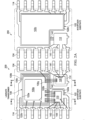
- FIG. 1 is a top perspective view that shows an example multi-chip ISO device package 100 which includes a first IC die 110 including circuitry comprising a transmitter or a receiver, and a second IC die 120 including circuitry comprising a transmitter or a receiver so that the package provides at least one communication channel.
- the ISO device package 100 also comprises a laminate transformer 130 that is mounted to an interposer substrate 122 (e.g., a DBC substrate, such as for its dielectric layer 122b including ceramic such as Alumina (Al 2 O 3 ), Aluminum Nitride (AlN), or silicon nitride) including a top copper layer 122a and a bottom metal layer 122c with the dielectric layer 122b between these metal layers.
- an interposer substrate 122 e.g., a DBC substrate, such as for its dielectric layer 122b including ceramic such as Alumina (Al 2 O 3 ), Aluminum Nitride (AlN), or silicon nitride
- a laminate transformer 130 is on the top copper layer 122a, where the transformer 130 is coupled between the transmitter and the receiver of the respective IC die 110, 120 which provides reinforced isolation.
- the laminate transformer 130 generally supports a root mean square (RMS) breakdown voltage of at least 1 kV for a test time of one minute, typically providing a breakdown voltage of at least 2.5kV to 5kV.
- RMS root mean square
- UCC12050 has a breakdown test for a minute pursuant to UL1577 which is one of the most popular standards for isolation devices.
- the interposer substrate can comprise substrates besides DBC substrates, such as for example an insulated metal substrate (IMS) which can also be used as the interposer.
- IMS insulated metal substrate
- An IMS as known in the art comprises of a metal baseplate (aluminum is commonly used because of its low cost and density) covered by a thin layer of dielectric (usually an epoxy-based layer, typically FR-4) and a top layer of copper (generally about 35 ⁇ m to more than 200 ⁇ m thick).
- the FR-4-based dielectric is usually provided thin (about 100 ⁇ m thick) because it has lower thermal conductivity as compared to the ceramics used in DBC substrates.
- the interposer substrate can also include an active metal brazed substrates (AMB), where a metal foil is soldered to a ceramic using a solder paste.
- AMB is generally a higher cost arrangement compared to DBC, but technically, AMB has essentially the same configuration as DBC.
- the laminate transformer 130 generally during ISO device package operation being the hottest component in the ISO device package being attached to the top copper layer 122a of the interposer substrate 122 enables the heat generated by the laminate transformer 130 to be vertically conducted away.
- the heat transfer path for the ISO device package 100 is first through the top copper layer 122a, then through the dielectric layer 122b, and then finally out the bottom metal layer 122c to the ambient which functions as a heatsink for the ISO device package 100.
- the dielectric layer 122b can comprise a ceramic layer, which can provide a thermal conductivity at 20 0 C of at least 20 W/m ⁇ K.
- alumina has a Thermal Conductivity at 20 0 C of 28 to 35 W/m ⁇ K
- aluminum nitride has a Thermal Conductivity at 20 0 C of about 70 to 180 W/m K
- silicon nitride has Thermal Conductivity of about 30 W/m K at 20 0 C.
- the interposer substrate 122 is shown by example for the ISO device package 100 in FIG. 1 being L-shaped to accommodate the laminate transformer 130 and the second IC die 120.
- the first IC die 110 is lateral to the area of interposer substrate 122, and is instead on a die pad 112 of the leadframe that is lateral to the area of the interposer substrate 122.
- the interposer substrate 122 can also in some disclosed arrangements occupy essentially the whole area of the ISO device package so that the laminate transformer 130 and the first and second IC die 110, 120 are all on a patterned top copper layer 122a portion of the interposer substrate 122. This arrangement is shown in FIG. 2D described below. In another arrangement, the interposer substrate 122 takes up only enough area of the package so that the laminate transformer 130 is thereon, and there are separate die pads of a leadframe for the first IC die 110 and for the second IC die 120. This other arrangement is shown in FIG. 2E described below.
- the bottom metal layer 122c can comprise copper or aluminum.
- the first IC die 110 which includes circuitry 180a and bond pads 181a is shown on the die pad 112, while the second IC die 120 including circuitry 180b and bond pads 181b is shown on the top copper layer 122a of the interposer substrate 122.
- the circuitry 180a, 180b on the IC die 110, 120 as known in the art comprises circuit elements (including transistors, and generally diodes, resistors, capacitors, etc.) formed in the semiconductor substrate, such as in an epitaxial layer on the bulk substrate material, configured together for generally realizing each at least a transmitter or receiver, with at least one of the IC die providing at least one additional circuit function.
- Example additional circuit functions include analog (e.g., amplifier, or a power converter), radio frequency (RF), digital, or non-volatile memory functions.
- the top copper layer 122a is etched or otherwise patterned to allow electrically isolating the second IC die 120 from the laminate transformer 130.
- the top copper layer 122a is patterned to isolate the first and second IC die 110, 120 from one another, and to provide isolation from the laminate transformer 130.
- Leads are shown as 124 on one side of the ISO device package 100, and leads 114 are shown on the other side of the ISO device package 100 opposite to the leads 124.
- a laminate dielectric 130b generally comprises a laminate substrate that has multiple metal layers (levels) with via connections through a dielectric material between the respective metal layers to bring all signals to a topmost surface of the laminate substrate.
- the bondwires 142, 143 between the IC die 110, 120 and the laminate transformer 130 will generally make connections to the topmost copper layer of the laminate substrate that are connected to either the top core (shown as coil 2) or bottom core (shown as coil 1) of the laminate transformer 130.
- bondwires 143 between some of the bond pads 130g on the laminate transformer 130 and some of the bond pads 181b on the second IC die 120, and some bondwires 144 between some of the bond pads 181b on the second IC die 120 and some of the leads 114.
- bondwires 145 between some of the bond pads 130g on the laminate transformer 130 and some of the leads 114.
- a mold compound 160 is also shown.
- the interposer substrate 122 is shown in FIG. 1 spanning an area of the ISO device package 100 sufficient to accommodate the laminate transformer 130 and one of the IC die shown as the second IC die 120, this need not be the case, such as in the case that the leadframe includes a first die pad and a second die pad for mounting the first IC die 110 and the second IC die 120.
- the top copper layer 122a of the interposer substrate 122 thus can have thereon either one of the two IC die and the laminate transformer 130, both of the IC die 110, 120 and the laminate transformer 130, or only the laminate transformer 130.
- the IC die 110, 120 can both be mounted on the dielectric layer 122b of the interposer substrate 122, or one or both IC die 110, 120 can have a separate area of the top copper layer 122a on the dielectric layer 122b to provide device isolation.
- the interposer substrate 122 comprises a DBC substrate
- a DBC substrate is typically more expensive than a leadframe arrangement, it is generally better to keep the area of the DBC substrate as small if possible.
- An advantage of a larger area DBC substrate with all components thereon is a thermal benefit. Having a large area top copper layer 122a helps the heat spreading by utilizing a larger area. Accordingly, for the ISO device package 100 there is a trade-off between cost and thermal performance.
- multi-chip ISO device package 100 shown in FIG. 1 includes only 2 IC die, 110, 120, disclosed multi-chip ISO device packages can have more than 2 IC die when desired.
- 3 IC die can be included instead of only 2 IC die in one disclosed multi-chip ISO device package. Accordingly, disclosed multi-chip ISO device packages provide scalability depending on the end application.
- Disclosed multichip IC device packages can generally be used for any power electronics circuit topology, not just for DC-DC converters. Examples beyond DC-DC converters can include a digital isolator, isolated flyback controller, isolated analog to digital converter (ADC), isolated gate driver, and isolated amplifiers.
- DC-DC converters can include a digital isolator, isolated flyback controller, isolated analog to digital converter (ADC), isolated gate driver, and isolated amplifiers.
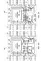
- FIG. 2A is a top view depiction example multi-chip ISO device package 200 which includes a laminate transformer 130 mounted to an interposer substrate 122, and first and second IC die 110, 120.
- the laminate transformer 130 generally comprises coil 1 (withN1 turns) and coil 2 (with N2 turns) each with magnetic field enhancing magnetic cores comprising a top magnetic core 130a and a bottom magnetic core 130c (that both typically comprise ferrite) which are spaced apart from one another by a laminate dielectric shown as 130b.
- the bottom view of this ISO device package 200 provided to the right of this FIG. shows the bottom metal layer 122c on the dielectric layer 122b of the interposer substrate 122. In this arrangement, analogous to FIG.
- the interposer substrate 122 again has an area large enough to accommodate the laminate transformer 130 as well is one of the IC die now shown as the first IC die 110, while the second IC die 120 is shown lateral to the area of the interposer substrate 122 instead being on a die pad 112 of the leadframe.
- FIG. 2B is a side cross-sectional view of the ISO device package 200 shown in FIG. 2A taken along the cut line A-A shown in FIG. 2A , where the top copper layer 122a is a patterned layer.
- FIG. 2B shows the first IC die 110 on a portion of the top copper layer 122a of the interposer substrate, having a bond pad 181a wirebonded by a bondwire 142 to a bond pad 130g of the laminate dielectric 130b of the laminate transformer 130 that is also on another portion of the top copper layer 122a.
- a mold compound 160 is shown, where the bottom metal layer 122c of the interposer substrate 122 is shown exposed from the ISO device package 200 to provide enhanced cooling for the laminate transformer 130.
- FIG. 2C is a side cross-sectional view of the ISO device package 200 shown in FIG. 2A taken along cut line B-B shown in FIG. 2A that shows the second IC die 120 on the die pad 112.
- the second IC die 120 has a bond pad 181b wirebonded to a bond pad 130g on the laminate dielectric 130b of the laminate transformer 130, where the laminate transformer 130 is on the top copper layer 122a of the interposer substrate 122.
- the second IC die 120 can be seen to be lateral to the interposer substrate 122, being instead on a die pad 112 of the leadframe.
- the bottom metal layer 122c of the interposer substrate 122 can again as in FIG. 2B be seen to be exposed from a bottom side of the ISO device package 200.
- Disclosed arrangements have freedom to select the cooling side of the ISO device package. For example, if the end application needs a topside cooling package, the backside of interposer substrate, such as copper for a DBC substrate, can also be exposed on topside of the ISO device package for topside heat sink attachment by flipping the view of the ISO device package 200 shown in FIG. 2C .
- FIG. 2D is a top view depiction example multi-chip ISO device package 240 which includes a laminate transformer 130 mounted to an interposer substrate shown as 122l.
- the interposer substrate 122l occupies essentially the whole area of the ISO device package 240 so that the laminate transformer 130 as well as the first IC die 110 and the second IC 120 are all on separate (patterned) areas of the top copper layer 122a of the interposer substrate 122l.
- FIG. 2E is a top view depiction example multi-chip ISO device package 260 which includes a laminate transformer 130 mounted onto an interposer substrate shown as 122s.
- the interposer substrate 122s takes up only enough area of the ISO device package 260 so that the laminate transformer 130 is thereon, and the leadframe provides separate die pads for the respective IC die, with a die pad 112a provided for the first IC die 110 and another die pad 112b provided for the second IC die 120.
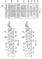
- FIG. 3 is a flow chart that shows steps in an example method 300 for forming multi-chip ISO device package that includes a laminate transformer mounted onto an isolating interposer substrate, according to an example aspect.
- Step 301 shown as "raw material preparation” comprises providing a first IC die 110, a second IC die 120, a laminate transformer 130, an interposer substrate 122, and a leadframe including leads or lead terminals (leads 114, 124 shown in FIG. 1 ) that optionally includes one or more die pad(s).
- the leadframe can include 0, 1, or 2 die pads, where the IC die can be either on die pads, or directly on the top copper layer of the interposer substrate where the top copper layer is optionally a patterned layer.
- the interposer substrate can have an area sufficient to accommodate all the components of the ISO device package, such as shown in FIG. 2D described above.
- Step 302 comprises mounting the leadframe (generally a leadframe panel/array) onto a fixture, and then picking and placing an interposer substrate inside the leads or lead terminals of the leadframe onto the fixture.
- the fixture can provide an accurate alignment between the leadframe and interposer substrate to enable placing the interposer substrate within an opening in the leadframe, and a tie-bar on the leadframe can be used to physically connect interposer substrates to the leadframe panel/array. This physical connection can be accomplished by using either an adhesive material along with reflow step, or using mechanical clamping.
- Step 303 comprises dispensing an adhesive on the top copper layer of the interposer substrate and optionally on one or more die pads.
- the adhesive generally has a thermal conductivity of at least 2 W/m ⁇ K @ 20 0 C, such as least 20 W/m ⁇ K @ 20 0 C.
- Step 304 comprises picking and placing the laminate transformer on the adhesive on the top copper layer of the interposer substrate, and the first IC die and second IC die on the adhesive on the top copper layer of the interposer substrate when the top copper layer is a patterned layer, or on the die pad(s) when the leadframe includes die pad(s).
- Step 305 comprises a curing or reflow process to cure the adhesive, such as curing at a temperature about 200°C for about a minute.
- Step 306 comprises wirebonding.
- Step 307 comprises a molding process to form a mold compound, and step 308 comprises package trim and forming, including cutting the tie-bars of the leadframe.
- the assembly can comprise configurations comprising a plurality of stacked semiconductor die.
- a variety of package substrates may be used.
- the semiconductor die may include various elements therein and/or layers thereon, including barrier layers, dielectric layers, device structures, active elements and passive elements including source regions, drain regions, bit lines, bases, emitters, collectors, conductive lines, conductive vias, etc.
- the semiconductor die can be formed from a variety of processes including bipolar, insulated-gate bipolar transistor (IGBT), CMOS, BiCMOS and MEMS.
Landscapes
- Engineering & Computer Science (AREA)
- Power Engineering (AREA)
- Lead Frames For Integrated Circuits (AREA)
- Manufacturing & Machinery (AREA)
- Semiconductor Integrated Circuits (AREA)
Abstract
Description
- This Disclosure relates to packaged semiconductor isolation (ISO) devices, and more particularly to packaged multi-chip ISO devices.
- In circuit designs for applications where high voltage (HV) is present, such as for motor control, it is generally necessary to take steps to reduce the potential risk to users of the electrical system. These steps traditionally include insulation, grounding, and the isolation of dangerous HV levels by establishing a dielectric separation from the HV. Techniques for passing signal information and power across a dielectric separation in a communication channel between integrated circuit (IC) die are known. A packaged ISO device prevents the propagation of direct current (DC) and unwanted AC currents between its input on one die and its output on the other die, while allowing the transmission of the desired AC signal between the die.
- The ISO device accomplishes this function using an isolation barrier between the first and second IC die that has a high breakdown voltage and low current leakage. A high resistance path exists across the isolation barrier, but the ISO device can still transfer information encoded in the desired AC signal across the isolation barrier from one IC die to the other by capacitive coupling, inductive coupling (transformer isolation), or by optical coupling. In the case of transformer isolation, a magnetic enhanced laminate transformer is known that comprises a coil 1 (with N1 turns) and a coil 2 (with N2 turns) with magnetic field enhancing magnetic cores comprising a top magnetic core and a bottom magnetic core that typically comprise ferrite.
- Some commercially available ISO devices comprise a DC/DC converter with a 5 kV root mean square (RMS) reinforced isolation rating designed to provide efficient, isolated power to isolated circuits that require a bias supply with a well-regulated output voltages. This ISO device includes a transformer and DC/DC controller that can provide 500 mW (typical) of isolated power with a high-power conversion efficiency and a low electromagnetic interference (EMI).
- Where isolation is used to enable the system to function properly, but not necessarily to serve as a barrier against electrical shock, it is conventionally called functional isolation. Where the isolation provides sufficient protection against electrical shock as long as the insulation barrier is intact, it is conventionally called basic isolation. Safety regulations require basic isolation to be supplemented with a secondary isolation barrier for redundancy, so that the additional barrier provides electrical shock protection, even if the first ISO-barrier fails. This is conventionally called double isolation. To make systems comprising ISO devices compact and to save cost, it is desirable to have only one level of isolation that has the required electrical strength, reliability, and shock protection conventionally provided by two levels of basic isolation. This isolation arrangement is conventionally called reinforced isolation.
- This Summary is provided to introduce a brief selection of disclosed concepts in a simplified form that are further described below in the Detailed Description including the drawings provided. This Summary is not intended to limit the claimed subject matter's scope.
- Disclosed aspects recognize compliance with creepage rules defined by various industrial standards such as underwriters laboratories (UL)1577, International Electrotechnical Commission (IEC)60747, and UL60950, limit the thermal dissipation capability of conventional reinforced ISO device packages (e.g., including two IC die supporting a DC/DC converter with IC die-IC die isolation) due to the absence of an exposed die pad, and thus prevents such ISO device packages from supporting high output power (e.g., > 1W) applications. The size of the ISO device package also is conventionally enlarged to meet the creepage requirements.
- Disclosed aspects include a solution to the above-described problem of conventional ISO device packages with reinforced isolation packages by adding an isolated interposer substrate, such and interposer substrate including as a thermally conductive dielectric layer between top and bottom metal layers that can both be copper. A disclosed ISO device package includes a first IC die including a transmitter or receiver and a second IC die including a transmitter or receiver, with a laminate transformer providing reinforced isolation coupled between the transmitter and the receiver on the respective IC die.
- Disclosed aspects include a multi-chip ISO device package includes a leadframe including leads, an interposer substrate including a top copper layer and a bottom metal layer, with a dielectric layer in-between. A first IC die and a second IC die both include circuitry including a transmitter or a receiver, and first bond pads on the first IC die and second bond pads on the second IC die are attached top side up in the package. A laminate transformer is attached to the top copper layer positioned lateral to the IC die. Bondwires wirebond the first bond pads to first pads on the laminate transformer and to a first group of the leads or the lead terminals, and bondwires wirebond the second bond pads to second pads on the laminate transformer and to a second group of the leads or the lead terminals, and a mold compound provides encapsulation for the ISO device package. The invention also relates to the following:
- 1. A multi-chip isolation (ISO) device package, comprising:
- a leadframe including leads or lead terminals,
- an interposer substrate comprising a top copper layer and a bottom metal layer, with a dielectric layer positioned between the top copper layer and the bottom metal layer;
- a first IC die comprising circuitry including a transmitter or a receiver and first bond pads attached top side up in the ISO device package;
- a second IC die comprising circuitry including a transmitter or a receiver and second bond pads attached top side up in the ISO device package;
- a laminate transformer attached to the top copper layer positioned lateral to the first and the second IC die;
- bondwires wirebonding respective ones of the first bond pads of the first IC die to first pads on the laminate transformer and to a first group of the leads or the lead terminals;
- bondwires wirebonding respective ones of the second bond pads of the second IC die to second pads on the laminate transformer and to a second group of the leads or the lead terminals, and
- a mold compound providing encapsulation for the ISO device package, wherein the bottom metal layer is exposed from the ISO device package at least under the laminate transformer.
- 2. The ISO device package of
item 1, wherein the interposer substrate comprises a direct bonded copper (DBC) substrate so that the bottom metal layer comprises copper. - 3. The multi-chip package of
item 1, wherein the circuitry for the first IC die or for the second IC die further comprises a DC/DC converter. - 4. The multi-chip package of
item 1, wherein the laminate transformer supports a root mean square (RMS) breakdown voltage of at least 1 kV. - 5. The multi-chip package of
item 1, wherein the top copper layer comprises a patterned layer. - 6. The multi-chip package of
item 1, wherein the dielectric layer comprises a ceramic layer which provides a thermal conductivity at 20 0C of at least 20 W/m K. - 7. The multi-chip package of
item 1, wherein the bottom metal layer is exposed from a bottom side or a topside of the ISO device package. - 8. The multi-chip package of
item 1, wherein the leadframe includes at least one die pad, and wherein the first IC die or the second IC die is attached top side up onto the die pad. - 9. The multi-chip package of
item 1, wherein the leadframe includes a first die pad and a second die pad, and wherein the first IC die is on the first die pad and the second IC die is on the second die pad. - 10. A method for forming a multi-chip isolation (ISO) device package, comprising:
- providing a first IC die including circuitry including a transmitter or a receiver and first bond pads, a second IC die including circuitry including a transmitter or a receiver and second bond pads, a laminate transformer, an interposer substrate comprising a top copper layer and a bottom metal layer with a dielectric layer positioned between the top copper layer and the bottom metal layer, and a leadframe including a plurality of leads or lead terminals;
- mounting the leadframe onto a fixture, and then picking and placing the interposer substrate inside the leads or lead terminals of the leadframe onto the fixture;
- dispensing an adhesive onto at least the top copper layer;
- picking and placing the laminate transformer, the first IC die, and the second IC die, onto the adhesive;
- curing the adhesive;
- wirebonding respective ones of the first bond pads of the first IC die to first pads on the laminate transformer and to a first group of the leads or the lead terminals, and respective ones of the second bond pads of the second IC die to second pads on the laminate transformer and to a second group of the leads or the lead terminals, and
- molding processing to form a mold compound for encapsulation for the ISO device package, wherein the bottom metal layer is exposed from the ISO device package at least under the laminate transformer.
- 11. The method of item 10, wherein the dispensing comprises positioning adhesive on the top copper layer when the top copper layer is a patterned layer, or on at least one die pad when the leadframe includes the die pad.
- 12. The method of item 10, wherein the adhesive has a thermal conductivity of at least 20 W/m·K at 20 0C.
- 13. The method of item 10, wherein the interposer substrate comprises a direct bonded copper (DBC) substrate so that the bottom metal layer comprises copper.
- 14. The method of item 10, wherein the top copper layer is a patterned layer.
- 15. The method of item 10, wherein the laminate transformer supports a root mean square (RMS) breakdown voltage of at least 1 kV.
- 16. The method of item 10, wherein the dielectric layer comprises a ceramic layer which provides a thermal conductivity at 20 0C of at least 20 W/m·K.
- 17. The method of item 10, wherein the leadframe includes at least one die pad, and wherein the picking and placing comprises placing the first IC die or the second IC die top side up onto the die pad.
- 18. The method of item 10, wherein the leadframe includes a first die pad and a second die pad, and wherein the picking and placing comprises placing the first IC die on the first die pad and the second IC die on the second die pad.
- 19. The method of item 10, wherein the leadframe comprises a leadframe panel.
- 20. The method of item 10, wherein the circuitry for the first IC die or for the second IC die further comprises a DC/DC converter.
- Reference will now be made to the accompanying drawings, which are not necessarily drawn to scale, wherein:
-
FIG. 1 is a top perspective view that shows an example multi-chip ISO device package which includes a first IC die including circuitry comprising a transmitter or a receiver, and a second IC die including circuitry comprising a transmitter or a receiver so that the package provides at least one communication channel, and a laminate transformer that is mounted to an interposer substrate that has a laminate transformer thereon that is coupled between the transmitter and the receiver of the respective IC die which provides reinforced isolation. -
FIG. 2A is a top view depiction example multi-chip ISO device package which includes a laminate transformer mounted to an interposer substrate. The bottom view of this ISO device package provided to the right of this FIG. shows the bottom metal layer on the dielectric layer of the interposer substrate. -
FIG. 2B is a side cross-sectional view of the ISO device package shown inFIG. 2A taken along cut line A-A shown inFIG. 2A , where the top copper layer is a patterned layer, that shows the first IC die on the top copper layer having a bond pad wirebonded to a bond pad on the laminate dielectric of the laminate transformer that is on the interposer substrate. -
FIG. 2C is a side cross-sectional view of the ISO device package shown inFIG. 2A taken along cut line B-B shown inFIG. 2A that shows the second IC die on a die pad having a bond pad wirebonded to a bond pad on the laminate dielectric of the laminate transformer which is on the top copper layer of the interposer substrate. -
FIG. 2D is a top view depiction example multi-chip ISO device package which includes a laminate transformer mounted onto an interposer substrate. In this arrangement, the top copper layer is a patterned layer, and the interposer substrate occupies essentially the whole area of the package so that the laminate transformer as well as the first IC die and second IC die are all on an area of the top copper layer of the interposer substrate. -
FIG. 2E is a top view depiction example multi-chip ISO device package which includes a laminate transformer mounted onto an interposer substrate. In this arrangement, the interposer substrate takes up only enough area of the package so that the laminate transformer is thereon, and there are separate die pads of a leadframe for the first IC die and for the second IC die. -
FIG. 3 is a flow chart that shows steps in an example method for forming multi-chip ISO device package that includes a laminate transformer that is mounted onto an interposer substrate, according to an example aspect. - Example aspects are described with reference to the drawings, wherein like reference numerals are used to designate similar or equivalent elements. Illustrated ordering of acts or events should not be considered as limiting, as some acts or events may occur in different order and/or concurrently with other acts or events. Furthermore, some illustrated acts or events may not be required to implement a methodology in accordance with this Disclosure.
- Also, the terms "coupled to" or "couples with" (and the like) as used herein without further qualification are intended to describe either an indirect or direct electrical connection. Thus, if a first device "couples" to a second device, that connection can be through a direct electrical connection where there are only parasitics in the pathway, or through an indirect electrical connection via intervening items including other devices and connections. For indirect coupling, the intervening item generally does not modify the information of a signal but may adjust its current level, voltage level, and/or power level.
- Disclosed aspects recognize the use of an interposer substrate, such as a direct bonded copper (DBC) substrate with a ceramic core dielectric layer having reasonably good thermal conductivity such as alumina or aluminum nitride, helps performance of the multi-chip ISO device package in at least 2 ways. The ceramic core material provides electrical isolation between the HV and low voltage nodes of the ISO device package within and external to the package. The generally thick top copper layer of the interposer substrate combined with the relatively high thermal conductivity of the ceramic material that the dielectric layer of the interposer substrate generally comprises help with enhanced heat dissipation which enables a higher power multi-chip ISO device package solution. Known multi-chip ISO device package solutions, such as the exposed die attach pad (DAP) small outline integrated circuit (SOIC) package, are non-isolated and generally also violate creepage requirements.
- Disclosed ISO devices generally provide the smallest area package with an exposed thermal pad which meets reinforced isolation requirements. The bottom thick copper layer of the interposer substrate provides the enhanced thermal transfer capability. The bottom copper layer also enables the attachment of a heat sink which will be isolated from the first IC die and second IC die components inside the package due to the dielectric nature of the core ceramic material.
-
FIG. 1 is a top perspective view that shows an example multi-chipISO device package 100 which includes a first IC die 110 including circuitry comprising a transmitter or a receiver, and a second IC die 120 including circuitry comprising a transmitter or a receiver so that the package provides at least one communication channel. TheISO device package 100 also comprises alaminate transformer 130 that is mounted to an interposer substrate 122 (e.g., a DBC substrate, such as for itsdielectric layer 122b including ceramic such as Alumina (Al2O3), Aluminum Nitride (AlN), or silicon nitride) including atop copper layer 122a and abottom metal layer 122c with thedielectric layer 122b between these metal layers. - A
laminate transformer 130 is on thetop copper layer 122a, where thetransformer 130 is coupled between the transmitter and the receiver of the respective IC die 110, 120 which provides reinforced isolation. Thelaminate transformer 130 generally supports a root mean square (RMS) breakdown voltage of at least 1 kV for a test time of one minute, typically providing a breakdown voltage of at least 2.5kV to 5kV. UCC12050 has a breakdown test for a minute pursuant to UL1577 which is one of the most popular standards for isolation devices. - The interposer substrate can comprise substrates besides DBC substrates, such as for example an insulated metal substrate (IMS) which can also be used as the interposer. An IMS as known in the art comprises of a metal baseplate (aluminum is commonly used because of its low cost and density) covered by a thin layer of dielectric (usually an epoxy-based layer, typically FR-4) and a top layer of copper (generally about 35 µm to more than 200 µm thick). The FR-4-based dielectric is usually provided thin (about 100 µm thick) because it has lower thermal conductivity as compared to the ceramics used in DBC substrates. As another alternate, the interposer substrate can also include an active metal brazed substrates (AMB), where a metal foil is soldered to a ceramic using a solder paste. AMB is generally a higher cost arrangement compared to DBC, but technically, AMB has essentially the same configuration as DBC.
- The
laminate transformer 130 generally during ISO device package operation being the hottest component in the ISO device package being attached to thetop copper layer 122a of theinterposer substrate 122 enables the heat generated by thelaminate transformer 130 to be vertically conducted away. The heat transfer path for theISO device package 100 is first through thetop copper layer 122a, then through thedielectric layer 122b, and then finally out thebottom metal layer 122c to the ambient which functions as a heatsink for theISO device package 100. - As noted above the
dielectric layer 122b can comprise a ceramic layer, which can provide a thermal conductivity at 20 0C of at least 20 W/m·K. For example, alumina has a Thermal Conductivity at 20 0C of 28 to 35 W/m·K, aluminum nitride has a Thermal Conductivity at 200C of about 70 to 180 W/m K, and silicon nitride has Thermal Conductivity of about 30 W/m K at 20 0C. - The
interposer substrate 122 is shown by example for theISO device package 100 inFIG. 1 being L-shaped to accommodate thelaminate transformer 130 and the second IC die 120. In this example, the first IC die 110 is lateral to the area ofinterposer substrate 122, and is instead on adie pad 112 of the leadframe that is lateral to the area of theinterposer substrate 122. - The
interposer substrate 122 can also in some disclosed arrangements occupy essentially the whole area of the ISO device package so that thelaminate transformer 130 and the first and second IC die 110, 120 are all on a patternedtop copper layer 122a portion of theinterposer substrate 122. This arrangement is shown inFIG. 2D described below. In another arrangement, theinterposer substrate 122 takes up only enough area of the package so that thelaminate transformer 130 is thereon, and there are separate die pads of a leadframe for the first IC die 110 and for the second IC die 120. This other arrangement is shown inFIG. 2E described below. - The
bottom metal layer 122c can comprise copper or aluminum. The first IC die 110 which includescircuitry 180a andbond pads 181a is shown on thedie pad 112, while the second IC die 120 includingcircuitry 180b andbond pads 181b is shown on thetop copper layer 122a of theinterposer substrate 122. Thecircuitry - The
top copper layer 122a is etched or otherwise patterned to allow electrically isolating the second IC die 120 from thelaminate transformer 130. In the case that the first and second IC die 110, 120 are both on thelaminate transformer 130, which is not shown inFIG. 1 , thetop copper layer 122a is patterned to isolate the first and second IC die 110, 120 from one another, and to provide isolation from thelaminate transformer 130. - Leads are shown as 124 on one side of the
ISO device package 100, and leads 114 are shown on the other side of theISO device package 100 opposite to theleads 124. There are bondwires shown as 141 between some of theleads 124 and some of thebond pads 181a on the first IC die 110, andbondwires 142 between some of thebond pads 181a on the first IC die 110 and some of thebond pads 130g on thelaminate dielectric 130b of thelaminate transformer 130. As known in the art, what is shown as alaminate dielectric 130b generally comprises a laminate substrate that has multiple metal layers (levels) with via connections through a dielectric material between the respective metal layers to bring all signals to a topmost surface of the laminate substrate. Accordingly, thebondwires laminate transformer 130 will generally make connections to the topmost copper layer of the laminate substrate that are connected to either the top core (shown as coil 2) or bottom core (shown as coil 1) of thelaminate transformer 130. - There are thus bondwires 143 between some of the
bond pads 130g on thelaminate transformer 130 and some of thebond pads 181b on the second IC die 120, and somebondwires 144 between some of thebond pads 181b on the second IC die 120 and some of theleads 114. There are also bondwires 145 between some of thebond pads 130g on thelaminate transformer 130 and some of theleads 114. Amold compound 160 is also shown. - Although the
interposer substrate 122 is shown inFIG. 1 spanning an area of theISO device package 100 sufficient to accommodate thelaminate transformer 130 and one of the IC die shown as the second IC die 120, this need not be the case, such as in the case that the leadframe includes a first die pad and a second die pad for mounting the first IC die 110 and the second IC die 120. Thetop copper layer 122a of theinterposer substrate 122 thus can have thereon either one of the two IC die and thelaminate transformer 130, both of the IC die 110, 120 and thelaminate transformer 130, or only thelaminate transformer 130. In this case thetop copper layer 122a is patterned, the IC die 110, 120 can both be mounted on thedielectric layer 122b of theinterposer substrate 122, or one or both IC die 110, 120 can have a separate area of thetop copper layer 122a on thedielectric layer 122b to provide device isolation. - It is noted that in the case that the
interposer substrate 122 comprises a DBC substrate, because a DBC substrate is typically more expensive than a leadframe arrangement, it is generally better to keep the area of the DBC substrate as small if possible. An advantage of a larger area DBC substrate with all components thereon (laminate transformer 130, the first IC die 110, and the second IC die 120) is a thermal benefit. Having a large areatop copper layer 122a helps the heat spreading by utilizing a larger area. Accordingly, for theISO device package 100 there is a trade-off between cost and thermal performance. - Although the multi-chip
ISO device package 100 shown inFIG. 1 includes only 2 IC die, 110, 120, disclosed multi-chip ISO device packages can have more than 2 IC die when desired. For example, 3 IC die can be included instead of only 2 IC die in one disclosed multi-chip ISO device package. Accordingly, disclosed multi-chip ISO device packages provide scalability depending on the end application. - Disclosed multichip IC device packages can generally be used for any power electronics circuit topology, not just for DC-DC converters. Examples beyond DC-DC converters can include a digital isolator, isolated flyback controller, isolated analog to digital converter (ADC), isolated gate driver, and isolated amplifiers.
-
FIG. 2A is a top view depiction example multi-chipISO device package 200 which includes alaminate transformer 130 mounted to aninterposer substrate 122, and first and second IC die 110, 120. Thelaminate transformer 130 generally comprises coil 1 (withN1 turns) and coil 2 (with N2 turns) each with magnetic field enhancing magnetic cores comprising a topmagnetic core 130a and a bottommagnetic core 130c (that both typically comprise ferrite) which are spaced apart from one another by a laminate dielectric shown as 130b. The bottom view of thisISO device package 200 provided to the right of this FIG. shows thebottom metal layer 122c on thedielectric layer 122b of theinterposer substrate 122. In this arrangement, analogous toFIG. 1 where only one of the IC die shown as the second IC die 120 and thelaminate transformer 130 are on theinterposer substrate 122, theinterposer substrate 122 again has an area large enough to accommodate thelaminate transformer 130 as well is one of the IC die now shown as the first IC die 110, while the second IC die 120 is shown lateral to the area of theinterposer substrate 122 instead being on adie pad 112 of the leadframe. -
FIG. 2B is a side cross-sectional view of theISO device package 200 shown inFIG. 2A taken along the cut line A-A shown inFIG. 2A , where thetop copper layer 122a is a patterned layer.FIG. 2B shows the first IC die 110 on a portion of thetop copper layer 122a of the interposer substrate, having abond pad 181a wirebonded by abondwire 142 to abond pad 130g of thelaminate dielectric 130b of thelaminate transformer 130 that is also on another portion of thetop copper layer 122a. Amold compound 160 is shown, where thebottom metal layer 122c of theinterposer substrate 122 is shown exposed from theISO device package 200 to provide enhanced cooling for thelaminate transformer 130. -
FIG. 2C is a side cross-sectional view of theISO device package 200 shown inFIG. 2A taken along cut line B-B shown inFIG. 2A that shows the second IC die 120 on thedie pad 112. The second IC die 120 has abond pad 181b wirebonded to abond pad 130g on thelaminate dielectric 130b of thelaminate transformer 130, where thelaminate transformer 130 is on thetop copper layer 122a of theinterposer substrate 122. The second IC die 120 can be seen to be lateral to theinterposer substrate 122, being instead on adie pad 112 of the leadframe. - The
bottom metal layer 122c of theinterposer substrate 122 can again as inFIG. 2B be seen to be exposed from a bottom side of theISO device package 200. Disclosed arrangements have freedom to select the cooling side of the ISO device package. For example, if the end application needs a topside cooling package, the backside of interposer substrate, such as copper for a DBC substrate, can also be exposed on topside of the ISO device package for topside heat sink attachment by flipping the view of theISO device package 200 shown inFIG. 2C . -
FIG. 2D is a top view depiction example multi-chipISO device package 240 which includes alaminate transformer 130 mounted to an interposer substrate shown as 122l. In this arrangement, the interposer substrate 122l occupies essentially the whole area of theISO device package 240 so that thelaminate transformer 130 as well as the first IC die 110 and thesecond IC 120 are all on separate (patterned) areas of thetop copper layer 122a of the interposer substrate 122l. -
FIG. 2E is a top view depiction example multi-chipISO device package 260 which includes alaminate transformer 130 mounted onto an interposer substrate shown as 122s. In this arrangement, theinterposer substrate 122s takes up only enough area of theISO device package 260 so that thelaminate transformer 130 is thereon, and the leadframe provides separate die pads for the respective IC die, with adie pad 112a provided for the first IC die 110 and anotherdie pad 112b provided for the second IC die 120. -
FIG. 3 is a flow chart that shows steps in anexample method 300 for forming multi-chip ISO device package that includes a laminate transformer mounted onto an isolating interposer substrate, according to an example aspect. Step 301 shown as "raw material preparation" comprises providing a first IC die 110, a second IC die 120, alaminate transformer 130, aninterposer substrate 122, and a leadframe including leads or lead terminals (leads 114, 124 shown inFIG. 1 ) that optionally includes one or more die pad(s). Depending on the package design, as described above, the leadframe can include 0, 1, or 2 die pads, where the IC die can be either on die pads, or directly on the top copper layer of the interposer substrate where the top copper layer is optionally a patterned layer. In the case the leadframe provides no die pads (only leads or lead terminals), the interposer substrate can have an area sufficient to accommodate all the components of the ISO device package, such as shown inFIG. 2D described above. - Step 302 comprises mounting the leadframe (generally a leadframe panel/array) onto a fixture, and then picking and placing an interposer substrate inside the leads or lead terminals of the leadframe onto the fixture. The fixture can provide an accurate alignment between the leadframe and interposer substrate to enable placing the interposer substrate within an opening in the leadframe, and a tie-bar on the leadframe can be used to physically connect interposer substrates to the leadframe panel/array. This physical connection can be accomplished by using either an adhesive material along with reflow step, or using mechanical clamping. Step 303 comprises dispensing an adhesive on the top copper layer of the interposer substrate and optionally on one or more die pads. As noted above, the adhesive generally has a thermal conductivity of at least 2 W/m·K @ 20 0C, such as least 20 W/m·K @ 20 0C.
- Step 304 comprises picking and placing the laminate transformer on the adhesive on the top copper layer of the interposer substrate, and the first IC die and second IC die on the adhesive on the top copper layer of the interposer substrate when the top copper layer is a patterned layer, or on the die pad(s) when the leadframe includes die pad(s). Step 305 comprises a curing or reflow process to cure the adhesive, such as curing at a temperature about 200°C for about a minute. Step 306 comprises wirebonding. Step 307 comprises a molding process to form a mold compound, and step 308 comprises package trim and forming, including cutting the tie-bars of the leadframe.
- Disclosed aspects can be integrated into a variety of assembly flows to form a variety of different multi-chip ISO packages and related products. The assembly can comprise configurations comprising a plurality of stacked semiconductor die. A variety of package substrates may be used. The semiconductor die may include various elements therein and/or layers thereon, including barrier layers, dielectric layers, device structures, active elements and passive elements including source regions, drain regions, bit lines, bases, emitters, collectors, conductive lines, conductive vias, etc. Moreover, the semiconductor die can be formed from a variety of processes including bipolar, insulated-gate bipolar transistor (IGBT), CMOS, BiCMOS and MEMS.
- Those skilled in the art to which this Disclosure relates will appreciate that many variations of disclosed aspects are possible within the scope of the claimed invention, and further additions, deletions, substitutions and modifications may be made to the above-described aspects without departing from the scope of this Disclosure.
Claims (15)
- A multi-chip isolation (ISO) device package, comprising:an interposer substrate comprising a top copper layer and a bottom metal layer, with a dielectric layer positioned between the top copper layer and the bottom metal layer;a laminate transformer attached to the top copper layer positioned lateral to a first IC die and a second IC die;bondwires wirebonding respective ones of first bond pads of the first IC die to first pads on the laminate transformer and to a first group of leads or lead terminals;bondwires wirebonding respective ones of second bond pads of a second IC die to second pads on the laminate transformer and to a second group of leads or lead terminals; anda mold compound providing encapsulation for the ISO device package, wherein the bottom metal layer is exposed from the ISO device package at least under the laminate transformer.
- The multi-chip package of claim 1, wherein the interposer substrate comprises a direct bonded copper (DBC) substrate so that the bottom metal layer comprises copper.
- The multi-chip package of claim 1, wherein the circuitry for the first IC die or for the second IC die further comprises a DC/DC converter.
- The multi-chip package of claim 1, wherein the laminate transformer supports a root mean square (RMS) breakdown voltage of at least 1 kV.
- The multi-chip package of claim 1, wherein the top copper layer comprises a patterned layer.
- The multi-chip package of claim 1, wherein the dielectric layer comprises a ceramic layer which provides a thermal conductivity at 20 0C of at least 20 W/m K.
- The multi-chip package of claim 1, wherein the bottom metal layer is exposed from a bottom side or a topside of the ISO device package.
- The multi-chip package of Claim 1, wherein a) the interposer substrate is not part of a leadframe; or b) the dielectric layer is not patterned.
- A method for forming a multi-chip isolation (ISO) device package, comprising:providing a laminate transformer;wirebonding respective ones of first bond pads of a first IC die to first pads on the laminate transformer and to a first group of leads or lead terminals, and respective ones of second bond pads of a second IC die to second pads on the laminate transformer and to a second group of leads or lead terminals, andcovering the laminate transformer, the first IC die and the second IC die and at least a portion of the first group of leads or lead terminals and at least a portion of the second group of leads or lead terminals with mold material, wherein the bottom metal layer is exposed from the ISO device package at least under the laminate transformer.
- The method of claim 9, further including placing an interposer substrate comprising a top copper layer and a bottom metal layer with a dielectric layer positioned between the top copper layer and the bottom metal layer, between the first IC die, the second IC die, the laminate transformer and the first group of leads or lead terminals and the second group of leads or lead terminals; optionally wherein the top copper layer is a patterned layer.
- The method of claim 9, wherein the dielectric layer comprises a ceramic layer which provides a thermal conductivity at 20 0C of at least 20 W/m K.
- A method for forming a device package, comprising:providing an interposer substrate comprising a top copper layer and a bottom metal layer with a dielectric layer positioned between the top copper layer and the bottom metal layer, and a leadframe including a plurality of leads or lead terminals;placing the interposer substrate inside leads or lead terminals;dispensing an adhesive onto at least the top copper layer;placing a laminate transformer, a first IC die, and a second IC die, onto the adhesive;wirebonding respective ones of the first bond pads of the first IC die to first pads on the laminate transformer and to a first group of the leads or the lead terminals, and respective ones of the second bond pads of the second IC die to second pads on the laminate transformer and to a second group of the leads or the lead terminals, andforming a mold material over the laminate transformer, the first IC die, and the second IC die, wherein the bottom metal layer is exposed from the ISO device package at least under the laminate transformer.
- The method of claim 9 or 12, wherein the interposer substrate comprises a direct bonded copper (DBC) substrate so that the bottom metal layer comprises copper.
- The method of claim 9 or 12, wherein the laminate transformer supports a root mean square (RMS) breakdown voltage of at least 1 kV.
- The method of claim 9 or 12, wherein the circuitry for the first IC die or for the second IC die further comprises a DC/DC converter.
Applications Claiming Priority (3)
| Application Number | Priority Date | Filing Date | Title |
|---|---|---|---|
| US16/828,298 US11329025B2 (en) | 2020-03-24 | 2020-03-24 | Multi-chip package with reinforced isolation |
| EP21776018.0A EP4128341B1 (en) | 2020-03-24 | 2021-03-23 | Multi-chip package with reinforced isolation |
| PCT/US2021/023563 WO2021195013A1 (en) | 2020-03-24 | 2021-03-23 | Multi-chip package with reinforced isolation |
Related Parent Applications (1)
| Application Number | Title | Priority Date | Filing Date |
|---|---|---|---|
| EP21776018.0A Division EP4128341B1 (en) | 2020-03-24 | 2021-03-23 | Multi-chip package with reinforced isolation |
Publications (2)
| Publication Number | Publication Date |
|---|---|
| EP4443506A2 true EP4443506A2 (en) | 2024-10-09 |
| EP4443506A3 EP4443506A3 (en) | 2024-12-18 |
Family
ID=77857524
Family Applications (2)
| Application Number | Title | Priority Date | Filing Date |
|---|---|---|---|
| EP24189578.8A Pending EP4443506A3 (en) | 2020-03-24 | 2021-03-23 | Multi-chip package with reinforced isolation |
| EP21776018.0A Active EP4128341B1 (en) | 2020-03-24 | 2021-03-23 | Multi-chip package with reinforced isolation |
Family Applications After (1)
| Application Number | Title | Priority Date | Filing Date |
|---|---|---|---|
| EP21776018.0A Active EP4128341B1 (en) | 2020-03-24 | 2021-03-23 | Multi-chip package with reinforced isolation |
Country Status (4)
| Country | Link |
|---|---|
| US (2) | US11329025B2 (en) |
| EP (2) | EP4443506A3 (en) |
| CN (1) | CN115004364A (en) |
| WO (1) | WO2021195013A1 (en) |
Families Citing this family (8)
| Publication number | Priority date | Publication date | Assignee | Title |
|---|---|---|---|---|
| FR3127841B1 (en) | 2021-10-01 | 2026-03-06 | St Microelectronics Tours Sas | Transformer in a housing substrate |
| US11929311B2 (en) * | 2021-10-15 | 2024-03-12 | Texas Instruments Incorporated | Isolated semiconductor package with HV isolator on block |
| US20230378022A1 (en) * | 2022-05-20 | 2023-11-23 | Texas Instruments Incorporated | Power module integrated circuit package |
| US12489061B2 (en) | 2022-06-27 | 2025-12-02 | Texas Instruments Incorporated | Semiconductor device with multiple dies |
| CN115332212B (en) * | 2022-09-13 | 2026-02-24 | 天水华天科技股份有限公司 | SiP plastic packaging piece and production method thereof |
| WO2024069401A1 (en) * | 2022-09-28 | 2024-04-04 | Delphi Technologies Ip Limited | Systems and methods for three channel galvanic isolator for inverter for electric vehicle |
| CN118553627B (en) * | 2024-07-29 | 2024-12-20 | 杰华特微电子股份有限公司 | Multi-chip package structure and manufacturing method thereof |
| US20260041017A1 (en) * | 2024-07-31 | 2026-02-05 | Texas Instruments Incorporated | Microelectronics device package with isolation and ceramic interposer forming thermal pad |
Family Cites Families (34)
| Publication number | Priority date | Publication date | Assignee | Title |
|---|---|---|---|---|
| KR100993579B1 (en) * | 2002-04-30 | 2010-11-10 | 르네사스 일렉트로닉스 가부시키가이샤 | Semiconductor device and electronic device |
| US7064442B1 (en) * | 2003-07-02 | 2006-06-20 | Analog Devices, Inc. | Integrated circuit package device |
| DE102007012154B4 (en) * | 2007-03-12 | 2014-05-08 | Infineon Technologies Ag | Semiconductor module with semiconductor chips and method for producing the same |
| US7468547B2 (en) * | 2007-05-11 | 2008-12-23 | Intersil Americas Inc. | RF-coupled digital isolator |
| JP5332374B2 (en) * | 2008-07-25 | 2013-11-06 | サンケン電気株式会社 | Semiconductor device |
| JP2010244977A (en) * | 2009-04-09 | 2010-10-28 | Renesas Electronics Corp | Semiconductor device |
| KR101101490B1 (en) * | 2009-11-24 | 2012-01-03 | 삼성전기주식회사 | Wireless device with shield |
| US20120199960A1 (en) | 2011-02-07 | 2012-08-09 | Texas Instruments Incorporated | Wire bonding for interconnection between interposer and flip chip die |
| US9093434B2 (en) * | 2011-04-04 | 2015-07-28 | Rohm Co., Ltd. | Semiconductor device and method for manufacturing semiconductor device |
| DE102011100487A1 (en) * | 2011-05-04 | 2012-11-08 | Micronas Gmbh | Integrated passive component |
| US9035435B2 (en) * | 2012-11-14 | 2015-05-19 | Power Integrations, Inc. | Magnetically coupled galvanically isolated communication using lead frame |
| US8963622B2 (en) * | 2013-03-10 | 2015-02-24 | Microchip Technology Incorporated | Method and apparatus for generating regulated isolation supply voltage |
| US9250403B2 (en) * | 2013-04-26 | 2016-02-02 | Oracle International Corporation | Hybrid-integrated photonic chip package with an interposer |
| US20150004902A1 (en) * | 2013-06-28 | 2015-01-01 | John M. Pigott | Die-to-die inductive communication devices and methods |
| US10297572B2 (en) * | 2014-10-06 | 2019-05-21 | Mc10, Inc. | Discrete flexible interconnects for modules of integrated circuits |
| JP6522402B2 (en) * | 2015-04-16 | 2019-05-29 | ローム株式会社 | Semiconductor device |
| US9899282B2 (en) * | 2015-07-24 | 2018-02-20 | Infineon Technologies Americas Corp. | Robust high performance semiconductor package |
| US10497506B2 (en) * | 2015-12-18 | 2019-12-03 | Texas Instruments Incorporated | Methods and apparatus for isolation barrier with integrated magnetics for high power modules |
| US9837923B2 (en) | 2016-04-27 | 2017-12-05 | General Electric Company | Integrated power converter and transformer |
| US9905439B2 (en) * | 2016-04-29 | 2018-02-27 | Delta Electronics, Inc. | Power module package having patterned insulation metal substrate |
| US10056319B2 (en) * | 2016-04-29 | 2018-08-21 | Delta Electronics, Inc. | Power module package having patterned insulation metal substrate |
| US20190109061A1 (en) * | 2017-10-11 | 2019-04-11 | Texas Instruments Incorporated | Edge Bend for Isolation Packages |
| US10439065B2 (en) | 2017-10-11 | 2019-10-08 | Texas Instruments Incorporated | Inverted leads for packaged isolation devices |
| US11315891B2 (en) | 2018-03-23 | 2022-04-26 | Taiwan Semiconductor Manufacturing Company, Ltd. | Methods of forming semiconductor packages having a die with an encapsulant |
| US10714418B2 (en) * | 2018-03-26 | 2020-07-14 | Texas Instruments Incorporated | Electronic device having inverted lead pins |
| US10559524B1 (en) * | 2018-09-17 | 2020-02-11 | Texas Instruments Incorporated | 2-step die attach for reduced pedestal size of laminate component packages |
| US11482477B2 (en) * | 2018-12-31 | 2022-10-25 | Texas Instruments Incorporated | Packaged electronic device with suspended magnetic subassembly |
| US20200248914A1 (en) * | 2019-01-31 | 2020-08-06 | Johnson Controls Technology Company | Printed circuit board of an hvac controller |
| US10854538B2 (en) * | 2019-02-12 | 2020-12-01 | Texas Instruments Incorporated | Microelectronic device with floating pads |
| US11616006B2 (en) * | 2019-02-27 | 2023-03-28 | Semiconductor Components Industries, Llc | Semiconductor package with heatsink |
| US11258270B2 (en) * | 2019-06-28 | 2022-02-22 | Alpha And Omega Semiconductor (Cayman) Ltd. | Super-fast transient response (STR) AC/DC converter for high power density charging application |
| US20210193586A1 (en) * | 2019-12-18 | 2021-06-24 | Bae Systems Information And Electronic Systems Integration Inc. | Cryptographic system-in-package (csip) |
| JP7603400B2 (en) * | 2020-09-10 | 2024-12-20 | ローム株式会社 | Semiconductor Device |
| JP7527916B2 (en) * | 2020-09-29 | 2024-08-05 | ローム株式会社 | Semiconductor Device |
-
2020
- 2020-03-24 US US16/828,298 patent/US11329025B2/en active Active
-
2021
- 2021-03-23 CN CN202180011225.5A patent/CN115004364A/en active Pending
- 2021-03-23 EP EP24189578.8A patent/EP4443506A3/en active Pending
- 2021-03-23 WO PCT/US2021/023563 patent/WO2021195013A1/en not_active Ceased
- 2021-03-23 EP EP21776018.0A patent/EP4128341B1/en active Active
-
2022
- 2022-05-10 US US17/741,402 patent/US11908834B2/en active Active
Also Published As
| Publication number | Publication date |
|---|---|
| EP4443506A3 (en) | 2024-12-18 |
| US11329025B2 (en) | 2022-05-10 |
| WO2021195013A1 (en) | 2021-09-30 |
| US20220271008A1 (en) | 2022-08-25 |
| EP4128341B1 (en) | 2024-07-24 |
| EP4128341A1 (en) | 2023-02-08 |
| US20210305207A1 (en) | 2021-09-30 |
| EP4128341A4 (en) | 2023-09-13 |
| CN115004364A (en) | 2022-09-02 |
| US11908834B2 (en) | 2024-02-20 |
Similar Documents
| Publication | Publication Date | Title |
|---|---|---|
| EP4128341B1 (en) | Multi-chip package with reinforced isolation | |
| US10784213B2 (en) | Power device package | |
| JP7565365B2 (en) | DEVICE CARRIER CONFIGURED FOR INTERCONNECTING, PACKAGE MOUNTING DEVICE CARRIER HAVING INTERCONNECTING, AND METHOD OF MANUFACTURING SAME - Patent application | |
| KR20220162165A (en) | Multi-Level RF (RADIO FREQUENCY) Integrated Circuit Components Including Passive Devices | |
| US12142550B2 (en) | Multi-chip module leadless package | |
| US12015019B2 (en) | Stacked die multichip module package | |
| US5659462A (en) | Encapsulated, integrated power magnetic device and method of manufacture therefor | |
| US11153996B2 (en) | Thermal management assemblies for electronic assemblies mounted on a motor end | |
| KR102490612B1 (en) | Power semiconductor module | |
| US10888036B1 (en) | Thermal management assemblies for electronic assemblies circumferentially mounted on a motor | |
| US20200211934A1 (en) | Leadframe for multichip devices with thinned die pad portions | |
| US11749578B2 (en) | Semiconductor module, power semiconductor module, and power electronic equipment using the semiconductor module or the power semiconductor module | |
| US20200235067A1 (en) | Electronic device flip chip package with exposed clip | |
| CN108323211B (en) | Power device packaging | |
| CN111244061B (en) | Packaging structure of GaN devices | |
| US20240421139A1 (en) | Module assembly of multiple semiconductor devices with insulating substrates | |
| US20250372506A1 (en) | Isolation circuitry on semiconductor die | |
| EP4258337B1 (en) | Insulated board and power converter | |
| US11929311B2 (en) | Isolated semiconductor package with HV isolator on block | |
| US11791249B2 (en) | Thermally enhanced isolated power converter package | |
| US11521920B2 (en) | Plurality of power semiconductor chips between a substrate and leadframe | |
| KR100632237B1 (en) | 3D multilayer multichip module package manufacturing method |
Legal Events
| Date | Code | Title | Description |
|---|---|---|---|
| PUAI | Public reference made under article 153(3) epc to a published international application that has entered the european phase |
Free format text: ORIGINAL CODE: 0009012 |
|
| STAA | Information on the status of an ep patent application or granted ep patent |
Free format text: STATUS: THE APPLICATION HAS BEEN PUBLISHED |
|
| AC | Divisional application: reference to earlier application |
Ref document number: 4128341 Country of ref document: EP Kind code of ref document: P |
|
| AK | Designated contracting states |
Kind code of ref document: A2 Designated state(s): AL AT BE BG CH CY CZ DE DK EE ES FI FR GB GR HR HU IE IS IT LI LT LU LV MC MK MT NL NO PL PT RO RS SE SI SK SM TR |
|
| REG | Reference to a national code |
Ref country code: DE Ref legal event code: R079 Free format text: PREVIOUS MAIN CLASS: H01L0025160000 Ipc: H01L0023500000 |
|
| PUAL | Search report despatched |
Free format text: ORIGINAL CODE: 0009013 |
|
| AK | Designated contracting states |
Kind code of ref document: A3 Designated state(s): AL AT BE BG CH CY CZ DE DK EE ES FI FR GB GR HR HU IE IS IT LI LT LU LV MC MK MT NL NO PL PT RO RS SE SI SK SM TR |
|
| RIC1 | Information provided on ipc code assigned before grant |
Ipc: H01L 25/16 20230101ALI20241113BHEP Ipc: H01L 23/373 20060101ALI20241113BHEP Ipc: H01L 23/495 20060101ALI20241113BHEP Ipc: H01L 23/538 20060101ALI20241113BHEP Ipc: H01L 23/50 20060101AFI20241113BHEP |
|
| STAA | Information on the status of an ep patent application or granted ep patent |
Free format text: STATUS: REQUEST FOR EXAMINATION WAS MADE |
|
| 17P | Request for examination filed |
Effective date: 20250618 |
|
| REG | Reference to a national code |
Ref country code: DE Ref legal event code: R079 Free format text: PREVIOUS MAIN CLASS: H01L0023500000 Ipc: H10W0090000000 |
|
| RIC1 | Information provided on ipc code assigned before grant |
Ipc: H10W 90/00 20260101AFI20260115BHEP Ipc: H10W 40/25 20260101ALI20260115BHEP Ipc: H10W 70/40 20260101ALI20260115BHEP Ipc: H10W 74/10 20260101ALN20260115BHEP |
|
| GRAP | Despatch of communication of intention to grant a patent |
Free format text: ORIGINAL CODE: EPIDOSNIGR1 |
|
| STAA | Information on the status of an ep patent application or granted ep patent |
Free format text: STATUS: GRANT OF PATENT IS INTENDED |
|
| RIC1 | Information provided on ipc code assigned before grant |
Ipc: H10W 90/00 20260101AFI20260128BHEP Ipc: H10W 40/25 20260101ALI20260128BHEP Ipc: H10W 70/40 20260101ALI20260128BHEP Ipc: H10W 74/10 20260101ALN20260128BHEP Ipc: H10W 72/50 20260101ALN20260128BHEP Ipc: H10W 72/59 20260101ALN20260128BHEP Ipc: H10W 72/90 20260101ALN20260128BHEP Ipc: H10W 74/00 20260101ALN20260128BHEP |
|
| INTG | Intention to grant announced |
Effective date: 20260303 |