EP4443221A1 - Integration von fortgeschrittenen photonischen materialien in eine photonische siliciumplattform - Google Patents
Integration von fortgeschrittenen photonischen materialien in eine photonische siliciumplattform Download PDFInfo
- Publication number
- EP4443221A1 EP4443221A1 EP24168867.0A EP24168867A EP4443221A1 EP 4443221 A1 EP4443221 A1 EP 4443221A1 EP 24168867 A EP24168867 A EP 24168867A EP 4443221 A1 EP4443221 A1 EP 4443221A1
- Authority
- EP
- European Patent Office
- Prior art keywords
- waveguide
- layer
- wafer
- silicon
- photonic
- Prior art date
- Legal status (The legal status is an assumption and is not a legal conclusion. Google has not performed a legal analysis and makes no representation as to the accuracy of the status listed.)
- Pending
Links
Images


Classifications
-
- G—PHYSICS
- G02—OPTICS
- G02F—OPTICAL DEVICES OR ARRANGEMENTS FOR THE CONTROL OF LIGHT BY MODIFICATION OF THE OPTICAL PROPERTIES OF THE MEDIA OF THE ELEMENTS INVOLVED THEREIN; NON-LINEAR OPTICS; FREQUENCY-CHANGING OF LIGHT; OPTICAL LOGIC ELEMENTS; OPTICAL ANALOGUE/DIGITAL CONVERTERS
- G02F1/00—Devices or arrangements for the control of the intensity, colour, phase, polarisation or direction of light arriving from an independent light source, e.g. switching, gating or modulating; Non-linear optics
- G02F1/01—Devices or arrangements for the control of the intensity, colour, phase, polarisation or direction of light arriving from an independent light source, e.g. switching, gating or modulating; Non-linear optics for the control of the intensity, phase, polarisation or colour
- G02F1/03—Devices or arrangements for the control of the intensity, colour, phase, polarisation or direction of light arriving from an independent light source, e.g. switching, gating or modulating; Non-linear optics for the control of the intensity, phase, polarisation or colour based on ceramics or electro-optical crystals, e.g. exhibiting Pockels effect or Kerr effect
- G02F1/0305—Constructional arrangements
- G02F1/0316—Electrodes
-
- G—PHYSICS
- G02—OPTICS
- G02F—OPTICAL DEVICES OR ARRANGEMENTS FOR THE CONTROL OF LIGHT BY MODIFICATION OF THE OPTICAL PROPERTIES OF THE MEDIA OF THE ELEMENTS INVOLVED THEREIN; NON-LINEAR OPTICS; FREQUENCY-CHANGING OF LIGHT; OPTICAL LOGIC ELEMENTS; OPTICAL ANALOGUE/DIGITAL CONVERTERS
- G02F1/00—Devices or arrangements for the control of the intensity, colour, phase, polarisation or direction of light arriving from an independent light source, e.g. switching, gating or modulating; Non-linear optics
- G02F1/01—Devices or arrangements for the control of the intensity, colour, phase, polarisation or direction of light arriving from an independent light source, e.g. switching, gating or modulating; Non-linear optics for the control of the intensity, phase, polarisation or colour
- G02F1/03—Devices or arrangements for the control of the intensity, colour, phase, polarisation or direction of light arriving from an independent light source, e.g. switching, gating or modulating; Non-linear optics for the control of the intensity, phase, polarisation or colour based on ceramics or electro-optical crystals, e.g. exhibiting Pockels effect or Kerr effect
- G02F1/035—Devices or arrangements for the control of the intensity, colour, phase, polarisation or direction of light arriving from an independent light source, e.g. switching, gating or modulating; Non-linear optics for the control of the intensity, phase, polarisation or colour based on ceramics or electro-optical crystals, e.g. exhibiting Pockels effect or Kerr effect in an optical waveguide structure
-
- G—PHYSICS
- G02—OPTICS
- G02B—OPTICAL ELEMENTS, SYSTEMS OR APPARATUS
- G02B6/00—Light guides; Structural details of arrangements comprising light guides and other optical elements, e.g. couplings
- G02B6/10—Light guides; Structural details of arrangements comprising light guides and other optical elements, e.g. couplings of the optical waveguide type
- G02B6/12—Light guides; Structural details of arrangements comprising light guides and other optical elements, e.g. couplings of the optical waveguide type of the integrated circuit kind
- G02B6/12002—Three-dimensional structures
-
- G—PHYSICS
- G02—OPTICS
- G02B—OPTICAL ELEMENTS, SYSTEMS OR APPARATUS
- G02B6/00—Light guides; Structural details of arrangements comprising light guides and other optical elements, e.g. couplings
- G02B6/10—Light guides; Structural details of arrangements comprising light guides and other optical elements, e.g. couplings of the optical waveguide type
- G02B6/12—Light guides; Structural details of arrangements comprising light guides and other optical elements, e.g. couplings of the optical waveguide type of the integrated circuit kind
- G02B6/12004—Combinations of two or more optical elements
-
- G—PHYSICS
- G02—OPTICS
- G02B—OPTICAL ELEMENTS, SYSTEMS OR APPARATUS
- G02B6/00—Light guides; Structural details of arrangements comprising light guides and other optical elements, e.g. couplings
- G02B6/10—Light guides; Structural details of arrangements comprising light guides and other optical elements, e.g. couplings of the optical waveguide type
- G02B6/12—Light guides; Structural details of arrangements comprising light guides and other optical elements, e.g. couplings of the optical waveguide type of the integrated circuit kind
- G02B2006/12035—Materials
- G02B2006/1204—Lithium niobate (LiNbO3)
-
- G—PHYSICS
- G02—OPTICS
- G02F—OPTICAL DEVICES OR ARRANGEMENTS FOR THE CONTROL OF LIGHT BY MODIFICATION OF THE OPTICAL PROPERTIES OF THE MEDIA OF THE ELEMENTS INVOLVED THEREIN; NON-LINEAR OPTICS; FREQUENCY-CHANGING OF LIGHT; OPTICAL LOGIC ELEMENTS; OPTICAL ANALOGUE/DIGITAL CONVERTERS
- G02F1/00—Devices or arrangements for the control of the intensity, colour, phase, polarisation or direction of light arriving from an independent light source, e.g. switching, gating or modulating; Non-linear optics
- G02F1/01—Devices or arrangements for the control of the intensity, colour, phase, polarisation or direction of light arriving from an independent light source, e.g. switching, gating or modulating; Non-linear optics for the control of the intensity, phase, polarisation or colour
- G02F1/015—Devices or arrangements for the control of the intensity, colour, phase, polarisation or direction of light arriving from an independent light source, e.g. switching, gating or modulating; Non-linear optics for the control of the intensity, phase, polarisation or colour based on semiconductor elements having potential barriers, e.g. having a PN or PIN junction
- G02F1/025—Devices or arrangements for the control of the intensity, colour, phase, polarisation or direction of light arriving from an independent light source, e.g. switching, gating or modulating; Non-linear optics for the control of the intensity, phase, polarisation or colour based on semiconductor elements having potential barriers, e.g. having a PN or PIN junction in an optical waveguide structure
-
- G—PHYSICS
- G02—OPTICS
- G02F—OPTICAL DEVICES OR ARRANGEMENTS FOR THE CONTROL OF LIGHT BY MODIFICATION OF THE OPTICAL PROPERTIES OF THE MEDIA OF THE ELEMENTS INVOLVED THEREIN; NON-LINEAR OPTICS; FREQUENCY-CHANGING OF LIGHT; OPTICAL LOGIC ELEMENTS; OPTICAL ANALOGUE/DIGITAL CONVERTERS
- G02F2202/00—Materials and properties
- G02F2202/20—LiNbO3, LiTaO3
Definitions
- Embodiments presented in this disclosure generally relate to silicon photonics. More specifically, embodiments disclosed herein relate to middle-end-of-line (MEOL) integration of Lithium niobate and Barium titanate thin films in silicon photonic waveguides.
- MEOL middle-end-of-line
- silicon is self-limiting as a medium for optical modulation.
- Silicon exhibits two-photon absorption effects that result in free carrier absorption. Two photon absorption is a non-linear effect occurring within an optical waveguide that increase optical loss within the optical waveguide.
- Silicon modulators also have low energy efficiency due to permanent injection currents.
- silicon modulators employing a reverse biased p-n junction require a long phase modulation length in excess of 1 mm. The large footprint required by these devices is not suitable for high density optical circuits.
- forward biased PIN diodes suffer from low modulation speeds. The effect of these limitations is that silicon optical modulators suffer from poor function in high-speed modulation and non-linear modulation.
- One embodiment presented in this disclosure includes a method of manufacturing a photonic platform.
- the method includes providing a chiplet that includes a Pockels effect electro-optic layer and a substrate, bonding the chiplet to a photonic wafer such that the Pockels effect electro-optic layer is optically coupled to a waveguide disposed within the photonic wafer, and removing the substrate after bonding the chiplet to the photonic wafer.
- silicon photonic platform that includes a semiconductor wafer comprising a waveguide, a Pockels effect electro-optic layer disposed over, and optically coupled to, the waveguide, a first electrode electrically coupled to a first end of the Pockels effect electro-optic layer, and a second electrode electrically coupled to a second end of the Pockels effect electro-optic layer where a wafer bondline is disposed between the Pockels effect electro-optic layer and the waveguide.
- silicon-based modulators are commonly integrated into photonic devices.
- the silicon platform combines photonic and electronic elements on the same chip while capitalizing on a mature silicon wafer industry.
- the combination of developed silicon wafer manufacturing techniques and the well-known qualities of silicon semiconductors allows for low-cost production.
- silicon based optical modulators suffer from poor function in high-speed modulation and non-linear modulation.
- the examples and embodiments that follow include Pockels effects based devices permit high-speed, low-power electro-optical modulation and are effective non-linear modulators.
- Materials such as LN and BTO exhibit Pockels Effects.
- the application of LN or BTO within photonic platforms offers several advantages.
- One such advantage is that LN or BTO modulates optical signals through an electro-optic effect.
- the electro-optic effect permits modulation of a signal through change in phase shift due to an alteration of the refractive index of a crystal by an applied electric field.
- the electro-optic effects of the crystal can be broadly classified as either longitudinal electro-optic effects or transverse electro-optic effects. Longitudinal electro-optic effects describe changes to the crystal when an electric field is applied along the propagation direction of light.
- Transverse electro-optic effects describe changes to the crystal when an electric field is applied perpendicular to the direction of propagation of the light. Electro-optic effects have very short response times, on the order of 10 10 Hz. This very fast response time permit high-speed modulation of a propagating signal. Electro-optic materials exhibit modification of the refractive index of the material by the application of a direct current (DC) or low frequency electric field. The applied low frequency electric field is much lower than the optical frequency.
- DC direct current
- a modification of the refractive index may occur through polarization.
- the magnitude of material polarization is proportional to the strength of an applied electric field.
- the magnitude of the material polarization as a function of the applied external electric field is:
- ⁇ 0 ⁇ e
- 2 term is the Pockels effect.
- Pockels effect exhibits material polarization as a function of the square of the external field.
- the Pockels effect or Pockels electro-optic effects materializes as a change in birefringence induced by the electric field.
- n eo n x (1 - 1 2 ⁇ n x 2 E ⁇ 1 2 sn x 2 E 2 ).
- n x is the index of refraction
- ⁇ is the Pockels coefficient having units m/V
- E is the applied electric field
- s is the Kerr coefficient having units m 2 /V 2 . From this equation the change in the applied electric field alters the index of refraction by the Pockels effect term: 1 2 ⁇ n x 2 E .
- Pockels effect materials like LN or BTO can alter the phase, frequency, amplitude, and/or polarization of the effected signal.
- the embodiments described herein include a silicon photonic platform that includes a waveguide.
- the waveguide includes a LN or BTO layer for modulation of an optical signal carried by a silicon waveguide.
- LN or BTO layer and the silicon nitride layer form a ridge waveguide that modulates optical signals more efficiently, is easier to construction, and utilizes MEOL processes to improve manufacturing.
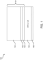
- Figure 1 illustrates a wafer 100 that has a substrate 101 and an electro-optical layer 105.
- the substrate 101 can have silicon substrate with option of having additional dielectric layer 103 (e.g., silicon dioxide) and an optional silicon layer 104.
- the electro-optical layer 105 can be LN or BTO.
- An optional dielectric layer 106 can be also deposited or formed on layer 105 to improve bonding properties of the final surface.
- the dielectric layer 106 can be used to bond the structure to another wafer.
- multiple chiplets can be cut from the wafer 100 and be placed (bonded) on a larger photonic platform in a manner where the LN or BTO layer 105 becomes part of a ridge waveguide.
- LN and BTO are electro-optic materials and the placement of the chiplet on a larger photonic platform is more simple, efficient, and effective than growing a LN or BTO layer directly on the larger photonic platform.
- LN or BTO waveguides use an applied electric field. Both LN and BTO exhibit electro-optic effects due to Pockels Effect.
- the ability of LN and BTO materials to change their bifringence through the application of an electric field creates efficient electro-optic modulators.
- LN has a melting point of 1250° C, a trigonal crystal system, a n o refractive index of 2.30, and a n e refractive index of 2.21.
- other applications for LN include high-performance acoustic wave filters.
- thin film LN on insulator wafers e.g., where the structure includes a silicon substrate/dielectric/LN layer
- Thin film LN wafers can be fabricated using a smart cut process by transferring a thin film of LN layer on a silicon wafer with insulator (typically oxide).
- BTO is used as the electro-optical material to make high-speed electro-optic modulators.
- BTO is a ferroelectric, pyroelectric, and piezoelectric ceramic material that has a melting point of 1,625° C, a tetragonal crystal system, a n o refractive index of 2.412, and a n e refractive index of 2.360.
- BTO enables Pockels-effect-based devices on silicon.
- Some of the benefits of applying BTO is its large Pockels coefficients, BTO can be grown on silicon substrates with large wafer sizes, and BTO exhibits excellent crystal quality.
- BTO is also a chemically and thermally stable material.
- BTO can be grown on wafers having a range of wafer diameters from 50mm to 300 mm independent of the diameter of the photonic platform wafer.
- BTO can be grown on silicon or insulator surface with good crystal quality.
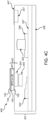
- FIG. 2 illustrates a photonic platform silicon on insulator (SOI) wafer 201 of a device 200 constructed by a front end of line (FEOL) process.
- the wafer 201 includes a photodiode 202 (e.g., a germanium photodiode) and a plurality of waveguides 203, 204, 205, 206, a buried oxide layer 207 and a silicon substrate 208.
- the waveguide 204 can be a silicon nitride waveguide or silicon waveguide.
- the waveguide 205 is an optional second silicon nitride waveguide.
- the waveguide 203 is a multi-level silicon waveguide and can be used to form grating couplers or wave-guiding structures. In one embodiment, the silicon waveguide 203 has a thickness less than 400nm.
- Photodiode 202 can also be integrated in the photonics platform wafer.
- Integration of thin film LN or BTO as part of a Middle End of Line (MEOL) process flow includes bonding LN or BTO chiplets after the FEOL which includes the formation of the Si and nitride waveguides 203, 204, 205, 206, germanium photodiode epitaxial and implants/anneals and prior to BEOL (Back End of Line) processing which includes metallization, Interlayer dielectric (ILD) formation and in some cases, wafer-to-wafer bonding.
- MOL Middle End of Line
- FIG. 3 illustrates one embodiment of MEOL attachment of a LN or BTO chiplet 301 to the photonic platform silicon wafer 201 to form a device 300. It should be noted here that other MEOL implementation of integration of LN or BTO chiplets on 210 are also possible.
- the chiplet 301 is bonded at a bond line at a top surface of the wafer 201.
- LN or BTO chiplets 301 are manufactured from the LN or BTO wafer 100.
- a single LN or BTO chiplet 301 die can be cut from the larger LN or BTO wafer 100.
- Each LN or BTO chiplet 301 has the same layers of the LN or BTO wafer 100.
- the layers 104 and 106 can be optional.
- the layers 103 and 106 can be made of silicon oxide or silicon nitride or any other integrated circuit fabrication compatible dielectric layers.
- the dimensions of the LN or BTO chiplets 301 is sized to match the required optic-electric signals carried by the waveguide.
- each chiplet 301 is bonded to the photonic wafer 201 in a MEOL process to form an electro-optic connection with waveguide 204.
- the union of the LN or BTO layer 105 with waveguide 204 forms a ridge waveguide structure capable of modulating the phase of the waveguide signal.
- Figure 4A illustrates the MEOL step of removing the first layer 102 (e.g., the substrate) of a device 400.
- the first layer 102 is removed.
- the final configuration of is a chiplet 401 electro-optically connected to the first nitride waveguide 204 forming a ridge waveguide 402.
- the layers 104 and 106 may be omitted.
- FIG 4B illustrates attaching a laser chiplet 403 (e.g., an III-V laser epi chiplet) to the photonic wafer 201, in addition to the BTO or LN chiplet 401.
- the position of the laser chiplet 403 is such that it will form ridge waveguide with the waveguide 204.
- the laser chiplet 403 can have Multiple Quantum Well (MQW) or Multiple Quantum Dot (MQD) structure 407.
- MQW Multiple Quantum Well
- MQD Multiple Quantum Dot
- a substrate 406 of the laser chiplet 403 is removed as shown in Figure 4C . This can be followed by additional MEOL and BEOL processing steps similar to shown in Figures 6-8 to convert the structure 407 into a laser structure.
- Figure 5 illustrates an additional embodiment of the device depicted in Figure 1 .
- a silicon nitride layer 501 is added during MEOL processing to the chiplet 401.
- the process steps to form silicon nitride layer 501 are not described and can include conventional IC fabrication process steps such as deposition, photolithography, etch, and chemical mechanical processing.
- the addition of the silicon nitride layer 501 improves phase efficiency and facilitates mode engineering.
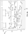
- FIG. 6 illustrates additional MEOL elements added to the device of Figure 4A to form device 600.
- Electrodes 602, 603 are added to connect the LN or BTO layer to an electric field.
- Electrode 602 is located distal from the midline of the LN or BTO layer.
- Electrode 603 is located distal from both electrode 602 and the midline of the LN or BTO layer.
- An electric charge applied to electrodes 602 and 603 induces an electric field in the ridge waveguide 402. The applied electric fields allow birefringence and phase adjusting.
- Additional elements include electrodes 604, 605, and 606, first level metal (M1-A) connection 607, a second first level metal connection (M1-B) 608, and nitride layers 609, 610, and 614.
- the nitride layers 609, 610, and 614 can be nitride caps to provide an upper diffusion barrier for the metal underneath.
- the layers 609, 610, and 614 are formed by a single layer deposition and etching using photolithography process.
- a waveguide e.g., a nitride waveguide
- Electrodes 602, 603, 604, 605, and 606 can be made using tungsten (W) or any other appropriate metals.
- Inter-metal dielectric layer (IDL) 601 may be formed using multiple deposition, etching, and polishing steps as part of the integration scheme to create metal separating dielectric.
- the IDL 601 can be tetraethyl orthosilicate (TEOS), silicon, silicon dioxide, or other suitable material, or a combination thereof.
- TEOS tetraethyl orthosilicate
- the laser structure 407 of Figure 4C can be added to the structure in Figure 6 , in which case additional steps can be performed to create metal contacts to the laser layer.
- Layers 611, 612, and 617 are diffusion barrier layers and are formed using a single deposition and etching using photolithography process.
- the choice of diffusion barrier layer is dependent on the choice of metal system used for the metal connections 607, 608, and 616.
- the M1-A connection 608 may also have a nitride layer 610 located on the proximal side of M1-A connection 608. Nitride layer 610 extends over both sides of M1-A connection 608. M1-A connection 608 forms an electrical connection with the LN or BTO layer 105 through electrode 603. M1-A connection 608 is connected to photodiode 202 through electrode 606. M1-A connection 608 is connected to waveguide 206 through electrode 605.
- a second first level metal connection 607 also has a nitride layer 609 located on the proximal side of M1-B 607.
- the connection 607 is connected to the LN or BTO layer 105 by way of electrode 602.
- An additional electrode 604 connects the connection 607 with waveguide 203.
- Connection 613 is a connection between M1 layers and second metal layer M2 above it (not shown in the figure). While not shown, addition BEOL processes can be performed on the device 600 to form a large number of additional metal layers (for example two to fifteen layers) with electrical connections between them.
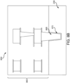
- FIG. 7 illustrates another embodiment in which a Through Silicon Via (TSV) 705 is also implemented prior to formation of M1 layer in a device 700.
- the TSV 705 extends from a metal connection 616 (which is part of the first metal layer) deep inside the Si substrate 208 and provides electrical connection to the back side of the wafer when wafer is thinned to reveal the TSV 705 from back side.
- Layer 710 is a dielectric that provides electrical isolation between the TSV 705 and substrate 208.
- Typical thickness of the silicon substrate 208 after thinning may be in the range of 50-125ums and additional processing steps can be performed to create additional layers on the back side of the wafer.
- a wafer-to-wafer bonding based BEOL flow is described in Figure 8A through 8D . It is to be noted that a large number of BEOL options are available and the process flow described here is not limiting.
- Figure 8A shows a silicon photonic wafer 800 with BTO or LN integration and two layers of metals (rather than just one metal layer as shown in Figure 6 ). That is, the wafer 800 illustrates a metal layer 801 being added above, and connected to, the IDL 601 to form two metal layers. It is to be noted that the wafer 800 can include any number of metal layers (e.g., only one metal layer or more than two metal layers).
- Figure 8B shows a separate handle wafer 850 that has two metal layers 860 disposed on silicon substrate 208.
- the wafer 850 may not include any metal layer (and can simply include a dielectric layer on top of the substrate 208). Or the wafer 850 can include only one metal layer, or more than two metal layers.
- the wafer 850 also includes an optional TSV 865 that is isolated by a dielectric 870 from the substrate 208.
- FIG 8C illustrates, after wafer bonding in Figure 8C , the substrate of the wafer 800 (e.g., a photonic wafer) is removed and a contact 885 (e.g., a via) is formed to at least one metal layer in the wafer 800. Further, in this example, an optional contact 886 (e.g., a via) is also formed to connect to at least one metal layer of the wafer 850 (assuming this handle wafer has a metal layer). After forming the contacts 885 and 886, additional metal layers can be formed that includes the metal routes 887 and 888 and additional contacts such as the contact 889.
- a contact 885 e.g., a via
- Figure 9 illustrates a method 900 of manufacture of the photonic platform.
- Method 900 can refer to the elements in Figures 1-8 .
- a chiplet 301 that includes a Pockels effect electro-optic layer (e.g., a BTO or LN layer) and a substrate (e.g., the substrate 101 in Figure 1 ) is provided.
- the chiplet 301 may include any of the optional other layers illustrated in Figure 1 .
- the chiplet is bonded during a MEOL process to a photonic wafer (e.g., wafer 201 in Figure 2 ) such that the Pockels effect electro-optic layer is optical coupled to a waveguide (e.g., waveguide 204 in Figure 2 ) disposed within the wafer.
- a photonic wafer e.g., wafer 201 in Figure 2
- a waveguide e.g., waveguide 204 in Figure 2
- the substrate of the chiplet is removed.
- the method 900 can include bonding the laser structure (e.g., the laser chiplet 403) to the wafer and removing its substrate 406.
- metal layers e.g., metal connections 607 and 608
- electrical connections e.g., connection 613
- additional waveguides are formed on the combined chiplet and photonic wafer structure.
- a handle wafer (e.g., wafer 850 in Figure 8C ) is attached to the combined chiplet and photonic wafer structure.
- backside metals can (optionally) be formed on the structure, such as the metal routes 888 and 887 shown in Figure 8D as part of a back end of line (BEOL) process. Note that this block is applicable to Figures 8A-8D and may not be used when forming the structures illustrated in Figures 6 and 7 .
- embodiments disclosed herein may be embodied as a system, method or computer program product. Accordingly, embodiments may take the form of an entirely hardware embodiment, an entirely software embodiment (including firmware, resident software, micro-code, etc.) or an embodiment combining software and hardware aspects that may all generally be referred to herein as a "circuit,” “module” or “system.” Furthermore, embodiments may take the form of a computer program product embodied in one or more computer readable medium(s) having computer readable program code embodied thereon.
- each block in the flowchart illustrations or block diagrams may represent a module, segment, or portion of code, which comprises one or more executable instructions for implementing the specified logical function(s).
- the functions noted in the block may occur out of the order noted in the Figures. For example, two blocks shown in succession may, in fact, be executed substantially concurrently, or the blocks may sometimes be executed in the reverse order, depending upon the functionality involved.
Landscapes
- Physics & Mathematics (AREA)
- Nonlinear Science (AREA)
- General Physics & Mathematics (AREA)
- Optics & Photonics (AREA)
- Engineering & Computer Science (AREA)
- Chemical & Material Sciences (AREA)
- Ceramic Engineering (AREA)
- Crystallography & Structural Chemistry (AREA)
- Microelectronics & Electronic Packaging (AREA)
- Optical Modulation, Optical Deflection, Nonlinear Optics, Optical Demodulation, Optical Logic Elements (AREA)
Applications Claiming Priority (1)
| Application Number | Priority Date | Filing Date | Title |
|---|---|---|---|
| US18/297,321 US20240337870A1 (en) | 2023-04-07 | 2023-04-07 | Integration of advanced photonic materials in silicon photonic platform |
Publications (1)
| Publication Number | Publication Date |
|---|---|
| EP4443221A1 true EP4443221A1 (de) | 2024-10-09 |
Family
ID=90719640
Family Applications (1)
| Application Number | Title | Priority Date | Filing Date |
|---|---|---|---|
| EP24168867.0A Pending EP4443221A1 (de) | 2023-04-07 | 2024-04-05 | Integration von fortgeschrittenen photonischen materialien in eine photonische siliciumplattform |
Country Status (2)
| Country | Link |
|---|---|
| US (1) | US20240337870A1 (de) |
| EP (1) | EP4443221A1 (de) |
Families Citing this family (2)
| Publication number | Priority date | Publication date | Assignee | Title |
|---|---|---|---|---|
| US20250130368A1 (en) * | 2023-10-20 | 2025-04-24 | Vanguard International Semiconductor Corporation | Silicon photonic platform, method for forming composite platform and method for forming silicon photonic platform |
| CN117254345B (zh) * | 2023-11-16 | 2024-05-03 | 湖北九峰山实验室 | 一种模块化的硅基异质光电集成架构及方法 |
Citations (2)
| Publication number | Priority date | Publication date | Assignee | Title |
|---|---|---|---|---|
| US10788689B1 (en) * | 2019-10-18 | 2020-09-29 | National Technology & Engineering Solutions Of Sandia, Llc | Heterogeneously integrated electro-optic modulator |
| US20220252913A1 (en) * | 2019-04-25 | 2022-08-11 | Advanced Micro Foundry Pte. Ltd | A hybrid cmos compatible electro-optic device |
Family Cites Families (10)
| Publication number | Priority date | Publication date | Assignee | Title |
|---|---|---|---|---|
| US6872985B2 (en) * | 2001-11-15 | 2005-03-29 | Hrl Laboratories, Llc | Waveguide-bonded optoelectronic devices |
| US6885789B2 (en) * | 2002-06-07 | 2005-04-26 | Fujitsu Limited | Optical switch fabricated by a thin film process |
| US9933566B2 (en) * | 2015-11-13 | 2018-04-03 | Cisco Technology, Inc. | Photonic chip with an evanescent coupling interface |
| US20210286203A1 (en) * | 2020-03-12 | 2021-09-16 | Imec Usa Nanoelectronics Design Center,Inc. | Method of fabricating an electro-optical device |
| US12147083B2 (en) * | 2020-12-16 | 2024-11-19 | Intel Corporation | Hybrid manufacturing for integrating photonic and electronic components |
| US11841563B2 (en) * | 2021-03-31 | 2023-12-12 | IMEC USA NANOELECTRONICS DESIGN CENTER, Inc. | Electro-optic modulators that include caps for optical confinement |
| WO2023038767A2 (en) * | 2021-08-16 | 2023-03-16 | University Of Southern California | Quantum chip optoelectronic interposer |
| CN115793294A (zh) * | 2021-09-10 | 2023-03-14 | 苏州湃矽科技有限公司 | 电光调制器及其制备方法 |
| WO2023167633A1 (en) * | 2022-03-04 | 2023-09-07 | Advanced Micro Foundry Pte Ltd | A hybrid silicon photonics modulator and method to manufacture the same |
| CN114660836B (zh) * | 2022-03-21 | 2026-01-30 | 上海曦智科技股份有限公司 | 电光调制器及其制造方法 |
-
2023
- 2023-04-07 US US18/297,321 patent/US20240337870A1/en active Pending
-
2024
- 2024-04-05 EP EP24168867.0A patent/EP4443221A1/de active Pending
Patent Citations (2)
| Publication number | Priority date | Publication date | Assignee | Title |
|---|---|---|---|---|
| US20220252913A1 (en) * | 2019-04-25 | 2022-08-11 | Advanced Micro Foundry Pte. Ltd | A hybrid cmos compatible electro-optic device |
| US10788689B1 (en) * | 2019-10-18 | 2020-09-29 | National Technology & Engineering Solutions Of Sandia, Llc | Heterogeneously integrated electro-optic modulator |
Non-Patent Citations (1)
| Title |
|---|
| MERE VIPHRETUO ET AL: "Design and Fabrication of Hybrid Lithium Niobate Electro-Optic Modulators", 2022 IEEE INTERNATIONAL CONFERENCE ON EMERGING ELECTRONICS (ICEE), IEEE, 11 December 2022 (2022-12-11), pages 1 - 4, XP034342837, DOI: 10.1109/ICEE56203.2022.10117674 * |
Also Published As
| Publication number | Publication date |
|---|---|
| US20240337870A1 (en) | 2024-10-10 |
Similar Documents
| Publication | Publication Date | Title |
|---|---|---|
| US10718904B2 (en) | Thin-film integration compatible with silicon photonics foundry production | |
| EP4443221A1 (de) | Integration von fortgeschrittenen photonischen materialien in eine photonische siliciumplattform | |
| US8871554B2 (en) | Method for fabricating butt-coupled electro-absorptive modulators | |
| CN102033332B (zh) | 利用晶片键合技术的光调制器 | |
| CN103998960B (zh) | 电子/光子集成电路架构及其制造方法 | |
| Beals et al. | Process flow innovations for photonic device integration in CMOS | |
| US11675126B1 (en) | Heterogeneous integration of an electro-optical platform | |
| JP2019215488A (ja) | 電気光学変調器 | |
| US20180373067A1 (en) | Electroabsorption optical modulator | |
| CN114660836B (zh) | 电光调制器及其制造方法 | |
| CN117908186B (zh) | 一种单片集成高速调制硅基光芯片及制备方法 | |
| US11009726B2 (en) | Electroab sorption optical modulator | |
| CN117254345B (zh) | 一种模块化的硅基异质光电集成架构及方法 | |
| KR20160087960A (ko) | 전계흡수 광변조 소자 및 그 제조 방법 | |
| TWI810493B (zh) | 介電光電相移器 | |
| CN119960214B (zh) | 硅/单晶薄膜锆钛酸铅异质集成光学平台及其制备方法 | |
| CN110045520A (zh) | 电光相位调制器 | |
| US11988939B2 (en) | Method for producing an electro-optical phase shifter based on ferroelectric materials | |
| WO2020245618A2 (zh) | 种电光调制器、光器件及光模块 | |
| US20250237827A1 (en) | Photonic device and fabricating method thereof | |
| CN113917714A (zh) | 具有脊形波导的单片硅上iii-v族光电调相器 | |
| US20250172831A1 (en) | Electro-optical modulators integrated with photodiodes | |
| US20260123516A1 (en) | Method for Fabrication of Bonded Chiplets and Related Structure | |
| US20260123475A1 (en) | Method for Integration of Chiplets and Related Structure | |
| CN119620441B (zh) | 基于胶体纳米晶的pn结注入型硅基电光调制器及制备方法 |
Legal Events
| Date | Code | Title | Description |
|---|---|---|---|
| PUAI | Public reference made under article 153(3) epc to a published international application that has entered the european phase |
Free format text: ORIGINAL CODE: 0009012 |
|
| STAA | Information on the status of an ep patent application or granted ep patent |
Free format text: STATUS: THE APPLICATION HAS BEEN PUBLISHED |
|
| AK | Designated contracting states |
Kind code of ref document: A1 Designated state(s): AL AT BE BG CH CY CZ DE DK EE ES FI FR GB GR HR HU IE IS IT LI LT LU LV MC ME MK MT NL NO PL PT RO RS SE SI SK SM TR |
|
| STAA | Information on the status of an ep patent application or granted ep patent |
Free format text: STATUS: REQUEST FOR EXAMINATION WAS MADE |
|
| 17P | Request for examination filed |
Effective date: 20250328 |