EP4443207A1 - Optical waveguide package and light source module - Google Patents
Optical waveguide package and light source module Download PDFInfo
- Publication number
- EP4443207A1 EP4443207A1 EP22901359.4A EP22901359A EP4443207A1 EP 4443207 A1 EP4443207 A1 EP 4443207A1 EP 22901359 A EP22901359 A EP 22901359A EP 4443207 A1 EP4443207 A1 EP 4443207A1
- Authority
- EP
- European Patent Office
- Prior art keywords
- optical waveguide
- light
- cladding layer
- core
- waveguide package
- Prior art date
- Legal status (The legal status is an assumption and is not a legal conclusion. Google has not performed a legal analysis and makes no representation as to the accuracy of the status listed.)
- Withdrawn
Links
Images


Classifications
-
- H—ELECTRICITY
- H10—SEMICONDUCTOR DEVICES; ELECTRIC SOLID-STATE DEVICES NOT OTHERWISE PROVIDED FOR
- H10H—INORGANIC LIGHT-EMITTING SEMICONDUCTOR DEVICES HAVING POTENTIAL BARRIERS
- H10H20/00—Individual inorganic light-emitting semiconductor devices having potential barriers, e.g. light-emitting diodes [LED]
- H10H20/80—Constructional details
- H10H20/85—Packages
-
- G—PHYSICS
- G02—OPTICS
- G02B—OPTICAL ELEMENTS, SYSTEMS OR APPARATUS
- G02B6/00—Light guides; Structural details of arrangements comprising light guides and other optical elements, e.g. couplings
- G02B6/0001—Light guides; Structural details of arrangements comprising light guides and other optical elements, e.g. couplings specially adapted for lighting devices or systems
- G02B6/0011—Light guides; Structural details of arrangements comprising light guides and other optical elements, e.g. couplings specially adapted for lighting devices or systems the light guides being planar or of plate-like form
- G02B6/0066—Light guides; Structural details of arrangements comprising light guides and other optical elements, e.g. couplings specially adapted for lighting devices or systems the light guides being planar or of plate-like form characterised by the light source being coupled to the light guide
- G02B6/0073—Light emitting diode [LED]
-
- G—PHYSICS
- G02—OPTICS
- G02B—OPTICAL ELEMENTS, SYSTEMS OR APPARATUS
- G02B6/00—Light guides; Structural details of arrangements comprising light guides and other optical elements, e.g. couplings
- G02B6/10—Light guides; Structural details of arrangements comprising light guides and other optical elements, e.g. couplings of the optical waveguide type
- G02B6/12—Light guides; Structural details of arrangements comprising light guides and other optical elements, e.g. couplings of the optical waveguide type of the integrated circuit kind
-
- G—PHYSICS
- G02—OPTICS
- G02B—OPTICAL ELEMENTS, SYSTEMS OR APPARATUS
- G02B6/00—Light guides; Structural details of arrangements comprising light guides and other optical elements, e.g. couplings
- G02B6/10—Light guides; Structural details of arrangements comprising light guides and other optical elements, e.g. couplings of the optical waveguide type
- G02B6/12—Light guides; Structural details of arrangements comprising light guides and other optical elements, e.g. couplings of the optical waveguide type of the integrated circuit kind
- G02B6/122—Basic optical elements, e.g. light-guiding paths
- G02B6/125—Bends, branchings or intersections
-
- G—PHYSICS
- G02—OPTICS
- G02B—OPTICAL ELEMENTS, SYSTEMS OR APPARATUS
- G02B6/00—Light guides; Structural details of arrangements comprising light guides and other optical elements, e.g. couplings
- G02B6/24—Coupling light guides
- G02B6/42—Coupling light guides with opto-electronic elements
-
- G—PHYSICS
- G02—OPTICS
- G02B—OPTICAL ELEMENTS, SYSTEMS OR APPARATUS
- G02B6/00—Light guides; Structural details of arrangements comprising light guides and other optical elements, e.g. couplings
- G02B6/24—Coupling light guides
- G02B6/42—Coupling light guides with opto-electronic elements
- G02B6/4201—Packages, e.g. shape, construction, internal or external details
- G02B6/4204—Packages, e.g. shape, construction, internal or external details the coupling comprising intermediate optical elements, e.g. lenses, holograms
- G02B6/4214—Packages, e.g. shape, construction, internal or external details the coupling comprising intermediate optical elements, e.g. lenses, holograms the intermediate optical element having redirecting reflective means, e.g. mirrors, prisms for deflecting the radiation from horizontal to down- or upward direction toward a device
-
- H—ELECTRICITY
- H01—ELECTRIC ELEMENTS
- H01S—DEVICES USING THE PROCESS OF LIGHT AMPLIFICATION BY STIMULATED EMISSION OF RADIATION [LASER] TO AMPLIFY OR GENERATE LIGHT; DEVICES USING STIMULATED EMISSION OF ELECTROMAGNETIC RADIATION IN WAVE RANGES OTHER THAN OPTICAL
- H01S5/00—Semiconductor lasers
- H01S5/02—Structural details or components not essential to laser action
- H01S5/022—Mountings; Housings
- H01S5/0225—Out-coupling of light
Definitions
- the present disclosure relates to an optical waveguide package and a light source module.
- Patent Literature 1 A known optical waveguide is described in, for example, Patent Literature 1.
- Patent Literature 1 Japanese Unexamined Patent Application Publication No. 10-308555
- an optical waveguide package includes a substrate including a first surface, a cladding layer on the first surface and including a facing surface facing the first surface and an opposite surface opposite to the facing surface including a recess, a plurality of element mount portions in the recess, and a core in the cladding layer.
- the core includes a plurality of light incident portions each including an incident end face located at an inner side surface of the recess, a merging portion in which the plurality of light incident portions merge, and a light emission portion located downstream from the merging portion and including an emission end face located at an outer side surface of the cladding layer.
- the first surface includes an exposed portion at least lateral to the merging portion in a plan view.
- a light source module includes the above optical waveguide package and a plurality of light emitting elements each mounted on a corresponding element mount portion of the plurality of element mount portions.
- Such devices each include an optical waveguide including a cladding located on a main surface of a substrate and a core located in the cladding.
- merging includes, in addition to superimposition of light beams with different wavelengths, merging of light beams guided to their respective optical channels and emitted through their respective emission end faces in, for example, a lens.
- optical waveguide package and the light source module may be oriented with any sides being upward or downward
- the optical waveguide package and the light source module herein are defined using the perpendicular coordinate system (X, Y, and Z) for convenience, in which the positive Z-direction is upward, and directional terms such as an upper surface or a lower surface is used accordingly.
- X-direction may be referred to as a first direction or a length direction.
- Y-direction may be referred to as a second direction or a width direction.
- Z-direction may be referred to as a third direction or a height direction.
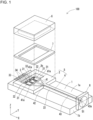
- FIG. 1 is an exploded perspective view of an optical waveguide package according to one embodiment of the present disclosure.
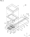
- FIG. 2 is an exploded perspective view of the optical waveguide package according to the embodiment of the present disclosure as viewed in a direction different from the direction in FIG. 1 .
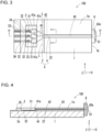
- FIG. 3 is a plan view of the optical waveguide package in FIG. 1 .
- FIG. 4 is a cross-sectional view taken along line IV-IV in FIG. 3 .
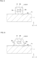
- FIG. 5 is an end view taken along line V-V in FIG. 3 .
- FIG. 6 is an end view of an optical waveguide package according to a variation of the optical waveguide package in FIG. 1 .
- FIG. 7 is an end view of an optical waveguide package according to a variation of the optical waveguide package in FIG. 1 .
- FIG. 1 is an exploded perspective view of an optical waveguide package according to one embodiment of the present disclosure.
- FIG. 2 is an exploded perspective view of the optical waveguide package according to the embodiment of the present disclosure as viewed in
- FIG. 8 is a plan view of an optical waveguide package according to a variation of the optical waveguide package in FIG. 1 .
- a lid and a loop seal are not illustrated.
- the end views in FIGs. 6 and 7 correspond to the end view in FIG. 5 .
- the plan view in FIG. 8 corresponds to the plan view in FIG. 3 .
- an optical waveguide package 100 includes a substrate 1, a cladding layer 2, multiple element mount portions 3, and a core 4.
- the substrate 1 includes a main surface (first surface) 1a and a side surface 1b continuous with the main surface 1a.
- the cladding layer 2 is located on the first surface 1a of the substrate 1.
- the cladding layer 2 includes a lower surface 2a facing the substrate 1 and an upper surface 2b opposite to the lower surface 2a.
- the upper surface 2b includes a recess 21.
- the multiple element mount portions 3 are located in the recess 21.
- Multiple light emitting elements 10 are mounted on the respective element mount portions 3.
- the core 4 is located in the cladding layer 2. The core 4 extends from the recess 21 to an outer side surface of the cladding layer 2.
- the substrate 1 may be a ceramic wiring board made of a ceramic material.
- the ceramic material used for the ceramic wiring board include sintered aluminum oxide, sintered mullite, sintered silicon carbide, sintered aluminum nitride, and sintered glass ceramic.
- the ceramic wiring board may include conductors such as connection pads, internal wiring conductors, and external connection terminals for electrical connection between the light emitting elements 10 and an external circuit.
- the ceramic wiring board may be a stack of multiple ceramic layers.
- the substrate 1 may be an organic wiring board made of an organic material.
- the organic wiring board may be a printed wiring board, a build-up wiring board, or a flexible wiring board.
- Examples of the organic material used for the organic wiring board include an epoxy resin, a polyimide resin, a polyester resin, an acrylic resin, a phenolic resin, and a fluororesin.
- the organic wiring board may be a single resin layer or may be a stack of multiple resin layers.
- the substrate 1 may be made of a compound semiconductor such as gallium nitride (GaN), gallium arsenide (GaAs), or indium phosphorus (InP), or may be made of silicon (Si), germanium (Ge), or sapphire (Al 2 O 3 ).
- GaN gallium nitride
- GaAs gallium arsenide
- InP indium phosphorus
- Si silicon
- germanium Ge
- sapphire Al 2 O 3
- the cladding layer 2 may be made of, for example, quartz (SiO 2 ).
- the cladding layer 2 may be a stack of layers.
- the cladding layer 2 may be a stack of a lower cladding layer located on the first surface 1a of the substrate 1 and an upper cladding layer located on the upper surface of the lower cladding layer.
- the core 4 may be located on the upper surface of the lower cladding layer.
- the recess 21 may extend through the cladding layer 2 in the height direction (Z-direction).
- the element mount portions 3 each include a first electrode pad 31 and a second electrode pad 32.
- the first electrode pad 31 is connected to a first wiring conductor 33.
- the second electrode pad 32 is connected to a second wiring conductor 34.
- the first wiring conductor 33 and the second wiring conductor 34 are located on the first surface 1a and extend from the inside of the recess 21 to the outside of the recess 21. The ends of the first wiring conductor 33 and the second wiring conductor 34 located outside the recess 21 is connected to an external power supply.
- the light emitting elements 10 mounted on the element mount portions 3 may be, for example, semiconductor laser diodes (LDs) or light-emitting diodes (LEDs).
- the multiple light emitting elements 10 may emit light beams of different wavelengths.
- the light emitting elements 10 may include a red-light emitting element 10r having a peak emission intensity in a red wavelength region (about 600 to 700 nm), a green-light emitting element 10g having a peak emission intensity in a green wavelength region (about 500 to 600 nm), and a blue-light emitting element 10b having a peak emission intensity in a blue wavelength region (about 400 to 500 nm).
- the element mount portions 3 may be separate from one another with multiple walls extending in the height direction (Z-direction).
- the walls may be integral with the cladding layer 2.
- the core 4 may be made of, for example, silicon oxynitride (SiON) or silicon oxide (SiOx).
- the optical waveguide package 100 includes the cladding layer 2 made of SiO 2 and the core 4 made of SiON.
- the core 4 has a higher refractive index than the cladding layer 2.
- the difference of the refractive index between the core 4 and the cladding layer 2 may be, for example, about 0.05 to 0.30.
- the optical waveguide package 100 includes the core 4 with a higher refractive index surrounded by the cladding layer 2 with a lower refractive index. Light propagating through the core 4 is totally reflected at the boundary between the core 4 and the cladding layer 2 to be confined in the core 4.
- the core 4 and the cladding layer 2 may be formed with, for example, photolithography and etching used in semiconductor device manufacturing.
- the cladding layer 2 and the core 4 are included in an optical waveguide 5 through which light beams emitted from the multiple light emitting elements mounted on the respective element mount portions 3 propagate.
- the core 4 includes multiple light incident portions 41, a merging portion 42, and a light emission portion 43.
- the light incident portions 41 each include an incident end face 41a located at an inner side surface of the recess 21.
- the multiple incident end faces 41a receive light beams emitted from the respective light emitting elements 10.
- the light incident portions 41 merge in the merging portion 42.
- the merging portion 42 may be a portion between a contact position at which the adjacent portions (light incident portions 41) of the core 4 are in contact with one another and a constant-width position at which the core 4 has a constant width downstream from the contact position.
- the light emission portion 43 is located downstream from the merging portion 42, or in other words, downstream from the merging portion 42 in a direction of light propagation.
- the light emission portion 43 extends in the first direction and includes an emission end face 43a located at an outer side surface of the cladding layer 2.
- the light emission portion 43 may have a width (dimension in Y-direction) of, for example, about 1 to 10 ⁇ m.
- the emission end face 43a of the light emission portion 43 and the outer side surface of the cladding layer 2 including the emission end face 43a are included in an output end 51 of the optical waveguide 5.
- the output end 51 of the optical waveguide 5 may be flush with the side surface 1b of the substrate 1. In this case, light emitted through the output end 51 is unlikely to hit the first surface 1a. Thus, light propagating through the light emission portion 43 can be output efficiently.
- the first surface 1a of the substrate 1 includes an exposed portion at least lateral to the merging portion 42 in a plan view. Being lateral herein refers to being in a direction perpendicular to an extension direction in which the light emission portion 43 extends and parallel to the first surface 1a.
- the merging portion 42 is a portion in which the multiple light incident portions 41 merge. Light beams propagating through the respective light incident portions 41 change their propagation directions in the merging portion 42 and are likely to leak from the core 4 in the merging portion 42.
- the optical waveguide package 100 which includes no portion of the cladding layer 2 in an area lateral to the merging portion 42, is likely to release light (hereafter also simply referred to as leaking light) leaking from the core 4 outside.
- the first surface 1a includes an exposed portion lateral to the merging portion 42 and the light emission portion 43 in the example in FIG. 3 , the first surface 1a may include an exposed portion lateral to the merging portion 42 alone without including an exposed portion lateral to the light emission portion 43.
- the optical waveguide package 100 which includes at least a portion of the optical waveguide 5 lateral to the merging portion 42 being narrower, is likely to release light emitted from the light emitting elements 10 and directly entering the cladding layer 2 outside from the narrower portion of the optical waveguide 5.
- the light emitted from the light emitting elements 10 and directly entering the cladding layer 2 is thus less likely to be emitted through the output end 51 of the optical waveguide 5.
- the optical waveguide package 100 which includes no portion of the cladding layer 2 on at least a part of the first surface 1a, allows less light (also referred to as external light) to enter the cladding layer 2 from the ambient environment. This can reduce external light to be stray light, which propagates through the cladding layer 2 to be emitted through the output end 51 of the optical waveguide 5.
- the optical waveguide package 100 reduces stray light emitted through the output end 51 of the optical waveguide 5 and allows emitted light to have higher quality.
- the cladding layer 2 in the optical waveguide package 100 may be formed by removing a portion of a precursor of the cladding layer 2 extending substantially throughout the first surface 1a.
- the portion of the precursor of the cladding layer 2 to be removed may be removed with photolithography and etching.
- the core 4 includes the light incident portions 41 having curvatures.
- the optical waveguide package 100 may include an exposed portion of the first surface 1a lateral to positions at which the curvatures of the respective light incident portions 41 are greatest.
- a two-dot-dash line L indicates an exposed portion of the first surface 1a extending to the portion lateral to the positions at which the curvatures of the respective light incident portions 41 are greatest. Light propagating through the core 4 is more likely to leak to the cladding layer 2 from a position at which the core 4 has a greater curvature.
- the exposed portion of the first surface 1a is located lateral to the position at which light is most likely to leak without no portion of the cladding layer 2 extending across an area lateral to the position.
- the optical waveguide package 100 is thus likely to release light leaking from the core 4 outside.
- light leaking from the core 4 is less likely to be stray light, which propagates through the cladding layer 2 to be emitted through the output end 51 of the optical waveguide 5. This can improve the quality of emitted light.
- the multiple light incident portions 41 may have different lengths in their extension direction (in the direction of light propagation). This structure can increase the flexibility in arranging the multiple element mount portions 3 and can reduce the size the optical waveguide package 100. Additionally, this structure decreases the curvatures of the light incident portions 41 and can reduce light leaking from the light incident portions 41.
- the optical waveguide package 100 may include an exposed portion of the first surface 1a lateral to the merging portion 42 and the light emission portion 43.
- the merging portion 42 and the light emission portion 43 are located downstream from the light incident portions 41.
- light leaking from the light incident portions 41 propagates through the portion of the cladding layer 2 covering the merging portion 42 and the light emission portion 43.
- the exposed portion of the first surface 1a located lateral to the merging portion 42 and the light emission portion 43, light (stray light) leaking from the light incident portions 41 is likely to be released outside. This can improve the quality of emitted light.
- Light leaking from the merging portion 42 is more likely to propagate in the positive first direction (rightward in FIG.
- the cladding layer 2 includes a narrow ridge 22 elongated along the core 4 in a portion lateral to the exposed portion of the first surface 1a.
- the ridge 22 includes, in a cross section perpendicular to the extension direction (X-direction) of the light emission portion 43, a second surface 22a facing the first surface 1a of the substrate 1, a third surface 22b opposite to the second surface 22a, a first side surface 22c continuous with the second surface 22a, and a second side surface 22d opposite to the first side surface 22c.
- the ridge 22 may have a width of about 1.5 to 30 times the width of the core 4 (light emission portion 43).
- the first side surface 22c and the second side surface 22d may be roughened.
- the first side surface 22c and the second side surface 22d may each have a greater surface roughness than the third surface 22b.
- This structure allows light leaking from the core 4 to be diffusely reflected at the boundary between the ridge 22 and the outside, thus reducing reentering of light leaking from the core 4 and reducing deterioration in the quality of emitted light.
- the first side surface 22c and the second side surface 22d may have an arithmetic mean roughness Ra of about 5 to 100 nm.
- the third surface 22b may have an arithmetic mean roughness Ra of about 0.1 to 10 nm.
- the first side surface 22c and the second side surface 22d may be inclined with respect to the first surface 1a, rather than at 90 degrees with respect to the first surface 1a.
- any light leaking from the core 4 and reflected at the boundary between the cladding layer 2 and the outside is less likely to be reflected toward the core 4. This can reduce reentering of light leaking from the core 4 and reduce deterioration in the quality of emitted light.
- the ridge 22 is tapered upward to have a smaller surface for external light to enter. This effectively reduces external light entering the cladding layer 2, thus effectively reducing external light to be stray light, which propagates through the optical waveguide 5 to be emitted through the output end 51 of the optical waveguide 5.
- the ridge 22 tapering upward allows stress generated between the ridge 22 and the substrate to disperse easily, improving the bonding reliably with the substrate 1.
- the first side surface 22c may be inclined with respect to the first surface 1a at an inclination angle ⁇ 1 greater than or equal to 70 degrees and less than 90 degrees.
- the second side surface 22d may be inclined with respect to the first surface 1a at an inclination angle ⁇ 2 greater than or equal to 70 degrees and less than 90 degrees.
- photolithography and etching may be used to form the first side surface 22c and the second side surface 22d easily.
- the inclination angle ⁇ 1 and the inclination angle ⁇ 2 may be the same or different.
- the ridge 22 may include a third side surface 22e continuous with the first side surface 22c, a fourth side surface 22f connecting the third side surface 22e and the third surface 22b, a fifth side surface 22g continuous with the second side surface 22d, and a sixth side surface 22h connecting the fifth side surface 22g and the third surface 22b.
- the ridge 22 has more corners, with the side surfaces of the ridge 22 having various angles with the first surface 1a.
- the fourth side surface 22f and the sixth side surface 22h may be inclined with respect to the first surface 1a.
- the fourth side surface 22f may be inclined with respect to the first surface 1a at an inclination angle ⁇ 4 that is greater than the inclination angle ⁇ 1 and the inclination angle ⁇ 2.
- the sixth side surface 22h may be inclined with respect to the first surface 1a at an inclination angle ⁇ 6 that is greater than the inclination angle ⁇ 1 and the inclination angle ⁇ 2.
- the inclination angle ⁇ 4 and the inclination angle ⁇ 6 may be greater than or equal to 70 degrees and less than 90 degrees. In this case, photolithography and etching may be used to form the fourth side surface 22f and the sixth side surface 22h easily.
- the third side surface 22e and the fifth side surface 22g may be substantially parallel to the first surface 1a of the substrate 1.
- the third side surface 22e and the fifth side surface 22g may each have a height that is the same as or different from the height of the first surface 1a
- the fourth side surface 22f and the sixth side surface 22h may be roughened.
- the fourth side surface 22f and the sixth side surface 22h may each have a greater surface roughness than the third surface 22b. This structure allows light leaking from the core 4 to be diffusely reflected at the boundaries between the fourth side surface 22f and the outside and between the sixth side surface 22h and the outside. This can reduce reentering of light leaking from the core 4 and reduce deterioration in the quality of emitted light.
- the fourth side surface 22f and the sixth side surface 22h may have an arithmetic mean roughness Ra of about 5 to 100 nm.
- the light emission portion 43 may be located adjacent to a corner of the profile of the ridge 22 in a cross section perpendicular to the extension direction (X-direction) of the light emission portion 43.
- any light leaking from the core 4 and reflected at the boundary between the cladding layer 2 and the outside is less likely to be reflected toward the core 4.
- Light leaking from the core 4 is thus less likely to reenter the core 4, allowing emitted light to have higher quality.
- the ridge 22 may include, on its side surface, at least one portion (also referred to as an acute angle surface) 24 that is closer to the core 4 toward the emission end face 43a and forms an acute angle with respect to an extension direction in which the core 4 extends.
- the ridge 22 may include the acute angle surface 24 on its side surface. Any leaking light entering the boundary between the acute angle surface 24 and the outside can have a smaller angle of incidence than leaking light entering the boundary between a portion of the cladding layer 2 other than the acute angle surface 24 and the outside.
- leaking light incident on the side surface being the acute angle surface 24 can enter the boundary between the side surface of the core 4 and the outside at a smaller angle of incidence than leaking light incident on a side surface of the ridge 22 extending parallel to the core 4.
- leaking light is less likely to be reflected at the boundary between the acute angle surface 24 and the outside and is more likely to be released outside. This can reduce stray light in the optical waveguide 5, improving the quality of emitted light.
- the acute angle surface 24 may have an inclination angle ⁇ 24, or in other words, an inclination angle ⁇ 24 of the acute angle surface 24 with respect to the extension direction (X-direction) of the core 4, that is set as appropriate for the emission angle of leaking light.
- the inclination angle ⁇ 24 may be, for example, 15 to 75 degrees. Leaking light is emitted at an acute angle with respect to the extension direction (X-direction). With the acute inclination angle ⁇ 24, the leaking light can enter the boundary between the acute angle surface 24 and the outside at an angle of incidence of 0 degrees or close to 0 degrees.
- the acute angle surface 24 may be at the same height as the core 4 from the first surface 1a and may be lateral to the core 4.
- the acute angle surface 24 may include a lower end below the lower end of the core 4 and an upper end above the upper end of the core 4. This structure can effectively reduce stray light in the optical waveguide 5 and can effectively improve the quality of emitted light.
- At least one acute angle surface 24 may be located lateral to the merging portion 42 in the ridge 22. Stray light of lower intensity can occur at other positions as well. Thus, as illustrated in FIG. 8 , multiple acute angle surfaces 24 may be located throughout the ridge 22 in the length direction (X-direction) to collectively define a saw-tooth shape. As illustrated in FIG. 8 , the acute angle surfaces 24 may be located on both ends of the ridge 22 in the second direction (Y-direction). The multiple acute angle surfaces 24 on the ridge 22 can effectively reduce stray light in the optical waveguide 5 and can effectively improve the quality of emitted light.
- the optical waveguide package 100 may further include a lid 6, a loop seal 7, and a condenser lens 8.
- the lid 6 is located on the upper surface 2b of the cladding layer 2 and closes the opening of the recess 21.
- the lid 6 may be directly bonded to the cladding layer 2 or may be bonded to the cladding layer 2 with the loop seal 7 between the lid 6 and the cladding layer 2 as illustrated in FIG. 1 .
- the loop seal 7 is looped and surrounds the opening of the recess 21 in a plan view. The loop seal 7 can improve the airtightness of the space accommodating the light emitting elements 10.
- the lid 6 may be directly bonded to the cladding layer 2 through, for example, heat bonding.
- the cladding layer 2 and the core 4 may deform under stress during bonding. This may cause misalignment of the optical axes between the light emitting elements 10 and the core 4.
- the loop seal 7 surrounding the opening of the recess 21 a portion of the cladding layer 2 close to the recess 21 can have higher mechanical strength. This can reduce deformation of the cladding layer 2 and the core 4 and misalignment of the optical axes between the light emitting elements 10 and the core 4.
- the lid 6 may be made of, for example, a glass material such as quartz, borosilicate glass, or sapphire.
- the lid 6 may be made of, for example, a metal material such as Fe, Ni, or Co or an alloy material containing any of these metals.
- the loop seal 7 may be made of, for example, a metal material such as Ti, Ni, Au, Pt, or Cr or an alloy material containing any of these metals.
- the loop seal 7 may be fixed to the upper surface 2b of the cladding layer 2 by, for example, vapor deposition, sputtering, ion plating, or plating.
- the lid 6 may be bonded to the loop seal 7 with a bond such as Au-Sn or Sn-Ag-Cu solder, a metal nanoparticle paste of, for example, Ag or Cu, or a glass paste.
- the condenser lens 8 is located on the optical path of light emitted through the emission end face 43a.
- the condenser lens 8 may collimate light emitted through the emission end face 43a or condense light emitted through the emission end face 43a.
- the condenser lens 8 may be a plano-convex lens with a flat incident surface facing the emission end face 43a and a convex emission surface.
- the optical waveguide package 100 may further include multiple first wiring conductors and multiple second wiring conductors located on the first surface 1a of the substrate 1.
- Each first wiring conductor includes one end connected to the corresponding first electrode pad and the other end extending outside the recess 21.
- Each second wiring conductor includes one end connected to the corresponding second electrode pad and the other end extending outside the recess 21. The other ends of the first wiring conductors and the other ends of the second wiring conductors are electrically connected to an external power supply circuit.
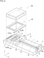
- FIG. 9 is an exploded perspective view of the light source module according to the embodiment of the present disclosure.
- a light source module 200 includes the optical waveguide package 100 and the multiple light emitting elements 10.
- the light emitting elements 10 may include the red-light emitting element 10r, the green-light emitting element 10g, and the blue-light emitting element 10b.
- the light emitting elements 10 are mounted on the respective element mount portions 3 in the optical waveguide package 100.
- the first electrodes are electrically connected to the respective first electrode pads 31 through conductive bonds
- the second electrodes are electrically connected to the respective second electrode pads 32 through connection members such as bonding wires.
- the green-light emitting element 10g, the red-light emitting element 10r, and the blue-light emitting element 10b are arranged in this order in the second direction (Y-direction) in the example in FIG. 9
- the light emitting elements 10 may be arranged in any order.
- the light emitting elements 10 are arranged to emit light beams in directions parallel to one another in the example in FIG. 9
- the light emitting elements 10 may be arranged to emit light beams in directions nonparallel to one another.
- the light source module 200 including the optical waveguide package 100 can emit light with high quality.
- FIG. 10 is a plan view of a light-emitting device according to another embodiment of the present disclosure.
- the core 4 includes three branching paths 41 and one joined path including the merging portion 42 in which the three branching paths 41 merge into the light emission portion 43 with one emission end face 43a.
- the light-emitting device including an optical waveguide package 100a includes optical channels for guiding light beams of different wavelengths individually.
- the light-emitting device includes three cores 4 that guide light beams of different wavelengths individually as in the example illustrated in the plan view in FIG. 10 .
- the three incident end faces 41a are located apart from one another to correspond to the positions of the respective light emitting elements 10, with the centers of the incident end faces 41a of the cores 4 aligned with the optical axes of the respective light emitting elements 10.
- the emission end faces 43a of the cores 4 are adjacent to one another. Light beams emitted through the respective emission end faces 43a merge in, for example, the lens 8 after traveling through a merging section extending between the incident end faces 41a and the emission end faces 43a in which the three cores 4 are gathered adjacent to one another and extend parallel to one another.
- the cores 4 may not be parallel to one another and may be substantially parallel to one another with the distances between them decreasing toward the output end.
- the cores 4 may bend greatly and be adjacent to one another before extending substantially parallel to one another toward the output end. In this structure, the distances between the adjacent cores 4 may decrease toward the output end. Merged light emitted through the lens 8 is divided by a downstream branching filter. As in the embodiment described above, when the separate three cores 4 are parallel to one another and are in contact with or adjacent to one another, the closely adjacent cores 3 have light coupling and substantially serve as a merging portion. Light beams emitted from the cores 4 may be emitted parallel to one another through, for example, one condenser lens 8. In this case, for example, images resulting from the light beams emitted through the three emission end faces 43a may be combined by, for example, an external device.
- the merging portion 42 is a portion in which a core 4 bends to approach another adjacent core 4 to be parallel to each other. More specifically, in FIG. 10 , the merging portion 42 extends from a position at which the cores 4 bend to be parallel to the linear core 4 to a position at which the cores 4 are parallel to one another.
- the light emission portion 43 is a portion in which the cores 4 extend parallel to one another. In the present embodiment, although the cores 4 do not actually merge in the merging portion, the cores 4 gather adjacent to one another as the merging portion.
- optical waveguide package according to one or more embodiments of the present disclosure may be implemented in forms 1 to 9 described below.
- the optical waveguide package reduces stray light emitted through the output end of the optical waveguide and allows emitted light to have higher quality.
- the light source module including the optical waveguide package described above can emit light with high quality.
Landscapes
- Physics & Mathematics (AREA)
- General Physics & Mathematics (AREA)
- Optics & Photonics (AREA)
- Engineering & Computer Science (AREA)
- Microelectronics & Electronic Packaging (AREA)
- Condensed Matter Physics & Semiconductors (AREA)
- Electromagnetism (AREA)
- Optical Integrated Circuits (AREA)
- Optical Couplings Of Light Guides (AREA)
Abstract
Description
- The present disclosure relates to an optical waveguide package and a light source module.
- A known optical waveguide is described in, for example,
Patent Literature 1. - Patent Literature 1:
Japanese Unexamined Patent Application Publication No. 10-308555 - In an aspect of the present disclosure, an optical waveguide package includes a substrate including a first surface, a cladding layer on the first surface and including a facing surface facing the first surface and an opposite surface opposite to the facing surface including a recess, a plurality of element mount portions in the recess, and a core in the cladding layer. The core includes a plurality of light incident portions each including an incident end face located at an inner side surface of the recess, a merging portion in which the plurality of light incident portions merge, and a light emission portion located downstream from the merging portion and including an emission end face located at an outer side surface of the cladding layer. The first surface includes an exposed portion at least lateral to the merging portion in a plan view.
- In an aspect of the present disclosure, a light source module includes the above optical waveguide package and a plurality of light emitting elements each mounted on a corresponding element mount portion of the plurality of element mount portions.
- The objects, features, and advantages of the present disclosure will become more apparent from the following detailed description and the drawings.
-
FIG. 1 is an exploded perspective view of an optical waveguide package according to one embodiment of the present disclosure. -
FIG. 2 is an exploded perspective view of the optical waveguide package according to the embodiment of the present disclosure as viewed in a direction different from the direction inFIG. 1 . -
FIG. 3 is a plan view of the optical waveguide package inFIG. 1 . -
FIG. 4 is a cross-sectional view taken along line IV-IV inFIG. 3 . -
FIG. 5 is an end view taken along line V-V inFIG. 3 . -
FIG. 6 is an end view of an optical waveguide package according to a variation of the optical waveguide package inFIG. 1 . -
FIG. 7 is an end view of an optical waveguide package according to a variation of the optical waveguide package inFIG. 1 . -
FIG. 8 is a plan view of an optical waveguide package according to a variation of the optical waveguide package inFIG. 1 . -
FIG. 9 is an exploded perspective view of a light source module according to one embodiment of the present disclosure. -
FIG. 10 is a plan view of an optical waveguide package according to another embodiment of the present disclosure. - Various devices such as light source modules and optical circuits that emit light of merged light beams emitted from multiple light emitting elements have been proposed as described in
Patent Literature 1. Such devices each include an optical waveguide including a cladding located on a main surface of a substrate and a core located in the cladding. - In such known devices, light leaking from the core or entering the cladding from the ambient environment may be stray light and emitted through an output end of the optical waveguide. This may lower the quality of emitted light.
- An optical waveguide package and a light source module according to one or more embodiments of the present disclosure will now be described with reference to the accompanying drawings. The drawings used herein are schematic and may not be drawn to scale relative to the actual size of each component. In embodiments of the present disclosure, merging includes, in addition to superimposition of light beams with different wavelengths, merging of light beams guided to their respective optical channels and emitted through their respective emission end faces in, for example, a lens. Although the optical waveguide package and the light source module according to one or more embodiments of the present disclosure may be oriented with any sides being upward or downward, the optical waveguide package and the light source module herein are defined using the perpendicular coordinate system (X, Y, and Z) for convenience, in which the positive Z-direction is upward, and directional terms such as an upper surface or a lower surface is used accordingly. X-direction may be referred to as a first direction or a length direction. Y-direction may be referred to as a second direction or a width direction. Z-direction may be referred to as a third direction or a height direction.
-
FIG. 1 is an exploded perspective view of an optical waveguide package according to one embodiment of the present disclosure.FIG. 2 is an exploded perspective view of the optical waveguide package according to the embodiment of the present disclosure as viewed in a direction different from the direction inFIG. 1 .FIG. 3 is a plan view of the optical waveguide package inFIG. 1 .FIG. 4 is a cross-sectional view taken along line IV-IV inFIG. 3 .FIG. 5 is an end view taken along line V-V inFIG. 3 .FIG. 6 is an end view of an optical waveguide package according to a variation of the optical waveguide package inFIG. 1 .FIG. 7 is an end view of an optical waveguide package according to a variation of the optical waveguide package inFIG. 1 .FIG. 8 is a plan view of an optical waveguide package according to a variation of the optical waveguide package inFIG. 1 . InFIGs. 3, 4 , and8 , a lid and a loop seal are not illustrated. The end views inFIGs. 6 and7 correspond to the end view inFIG. 5 . The plan view inFIG. 8 corresponds to the plan view inFIG. 3 . - In the present embodiment, an
optical waveguide package 100 includes asubstrate 1, acladding layer 2, multipleelement mount portions 3, and acore 4. - As illustrated in
FIGs. 1 to 3 , thesubstrate 1 includes a main surface (first surface) 1a and aside surface 1b continuous with themain surface 1a. Thecladding layer 2 is located on thefirst surface 1a of thesubstrate 1. As illustrated inFIG. 4 , thecladding layer 2 includes alower surface 2a facing thesubstrate 1 and anupper surface 2b opposite to thelower surface 2a. Theupper surface 2b includes arecess 21. The multipleelement mount portions 3 are located in therecess 21. Multiplelight emitting elements 10 are mounted on the respectiveelement mount portions 3. Thecore 4 is located in thecladding layer 2. Thecore 4 extends from therecess 21 to an outer side surface of thecladding layer 2. - The
substrate 1 may be a ceramic wiring board made of a ceramic material. Examples of the ceramic material used for the ceramic wiring board include sintered aluminum oxide, sintered mullite, sintered silicon carbide, sintered aluminum nitride, and sintered glass ceramic. The ceramic wiring board may include conductors such as connection pads, internal wiring conductors, and external connection terminals for electrical connection between thelight emitting elements 10 and an external circuit. The ceramic wiring board may be a stack of multiple ceramic layers. - The
substrate 1 may be an organic wiring board made of an organic material. The organic wiring board may be a printed wiring board, a build-up wiring board, or a flexible wiring board. Examples of the organic material used for the organic wiring board include an epoxy resin, a polyimide resin, a polyester resin, an acrylic resin, a phenolic resin, and a fluororesin. The organic wiring board may be a single resin layer or may be a stack of multiple resin layers. - The
substrate 1 may be made of a compound semiconductor such as gallium nitride (GaN), gallium arsenide (GaAs), or indium phosphorus (InP), or may be made of silicon (Si), germanium (Ge), or sapphire (Al2O3). - The
cladding layer 2 may be made of, for example, quartz (SiO2). Thecladding layer 2 may be a stack of layers. Thecladding layer 2 may be a stack of a lower cladding layer located on thefirst surface 1a of thesubstrate 1 and an upper cladding layer located on the upper surface of the lower cladding layer. Thecore 4 may be located on the upper surface of the lower cladding layer. Therecess 21 may extend through thecladding layer 2 in the height direction (Z-direction). - The
element mount portions 3 each include afirst electrode pad 31 and asecond electrode pad 32. Thefirst electrode pad 31 is connected to afirst wiring conductor 33. Thesecond electrode pad 32 is connected to asecond wiring conductor 34. Thefirst wiring conductor 33 and thesecond wiring conductor 34 are located on thefirst surface 1a and extend from the inside of therecess 21 to the outside of therecess 21. The ends of thefirst wiring conductor 33 and thesecond wiring conductor 34 located outside therecess 21 is connected to an external power supply. - The
light emitting elements 10 mounted on theelement mount portions 3 may be, for example, semiconductor laser diodes (LDs) or light-emitting diodes (LEDs). The multiplelight emitting elements 10 may emit light beams of different wavelengths. Thelight emitting elements 10 may include a red-lightemitting element 10r having a peak emission intensity in a red wavelength region (about 600 to 700 nm), a green-lightemitting element 10g having a peak emission intensity in a green wavelength region (about 500 to 600 nm), and a blue-light emitting element 10b having a peak emission intensity in a blue wavelength region (about 400 to 500 nm). - The
element mount portions 3 may be separate from one another with multiple walls extending in the height direction (Z-direction). The walls may be integral with thecladding layer 2. - The
core 4 may be made of, for example, silicon oxynitride (SiON) or silicon oxide (SiOx). In the present embodiment, theoptical waveguide package 100 includes thecladding layer 2 made of SiO2 and thecore 4 made of SiON. Thecore 4 has a higher refractive index than thecladding layer 2. The difference of the refractive index between thecore 4 and thecladding layer 2 may be, for example, about 0.05 to 0.30. Theoptical waveguide package 100 includes thecore 4 with a higher refractive index surrounded by thecladding layer 2 with a lower refractive index. Light propagating through thecore 4 is totally reflected at the boundary between thecore 4 and thecladding layer 2 to be confined in thecore 4. Thecore 4 and thecladding layer 2 may be formed with, for example, photolithography and etching used in semiconductor device manufacturing. - The
cladding layer 2 and thecore 4 are included in anoptical waveguide 5 through which light beams emitted from the multiple light emitting elements mounted on the respectiveelement mount portions 3 propagate. As illustrated inFIGs. 1 to 3 , thecore 4 includes multiplelight incident portions 41, a mergingportion 42, and alight emission portion 43. Thelight incident portions 41 each include anincident end face 41a located at an inner side surface of therecess 21. The multiple incident end faces 41a receive light beams emitted from the respectivelight emitting elements 10. Thelight incident portions 41 merge in the mergingportion 42. The mergingportion 42 may be a portion between a contact position at which the adjacent portions (light incident portions 41) of thecore 4 are in contact with one another and a constant-width position at which thecore 4 has a constant width downstream from the contact position. Thelight emission portion 43 is located downstream from the mergingportion 42, or in other words, downstream from the mergingportion 42 in a direction of light propagation. Thelight emission portion 43 extends in the first direction and includes anemission end face 43a located at an outer side surface of thecladding layer 2. Thelight emission portion 43 may have a width (dimension in Y-direction) of, for example, about 1 to 10 µm. Light beams emitted from thelight emitting elements 10 merge in the mergingportion 42 and are emitted through theemission end face 43a. Theemission end face 43a of thelight emission portion 43 and the outer side surface of thecladding layer 2 including theemission end face 43a are included in anoutput end 51 of theoptical waveguide 5. Theoutput end 51 of theoptical waveguide 5 may be flush with theside surface 1b of thesubstrate 1. In this case, light emitted through theoutput end 51 is unlikely to hit thefirst surface 1a. Thus, light propagating through thelight emission portion 43 can be output efficiently. - In the
optical waveguide package 100, thefirst surface 1a of thesubstrate 1 includes an exposed portion at least lateral to the mergingportion 42 in a plan view. Being lateral herein refers to being in a direction perpendicular to an extension direction in which thelight emission portion 43 extends and parallel to thefirst surface 1a. The mergingportion 42 is a portion in which the multiplelight incident portions 41 merge. Light beams propagating through the respectivelight incident portions 41 change their propagation directions in the mergingportion 42 and are likely to leak from thecore 4 in the mergingportion 42. Theoptical waveguide package 100, which includes no portion of thecladding layer 2 in an area lateral to the mergingportion 42, is likely to release light (hereafter also simply referred to as leaking light) leaking from thecore 4 outside. Thus, light leaking from thecore 4 is less likely to be stray light that propagates through thecladding layer 2. Although thefirst surface 1a includes an exposed portion lateral to the mergingportion 42 and thelight emission portion 43 in the example inFIG. 3 , thefirst surface 1a may include an exposed portion lateral to the mergingportion 42 alone without including an exposed portion lateral to thelight emission portion 43. - The
optical waveguide package 100, which includes at least a portion of theoptical waveguide 5 lateral to the mergingportion 42 being narrower, is likely to release light emitted from thelight emitting elements 10 and directly entering thecladding layer 2 outside from the narrower portion of theoptical waveguide 5. The light emitted from thelight emitting elements 10 and directly entering thecladding layer 2 is thus less likely to be emitted through theoutput end 51 of theoptical waveguide 5. - The
optical waveguide package 100, which includes no portion of thecladding layer 2 on at least a part of thefirst surface 1a, allows less light (also referred to as external light) to enter thecladding layer 2 from the ambient environment. This can reduce external light to be stray light, which propagates through thecladding layer 2 to be emitted through theoutput end 51 of theoptical waveguide 5. - As described above, the
optical waveguide package 100 reduces stray light emitted through theoutput end 51 of theoptical waveguide 5 and allows emitted light to have higher quality. - The
cladding layer 2 in theoptical waveguide package 100 may be formed by removing a portion of a precursor of thecladding layer 2 extending substantially throughout thefirst surface 1a. The portion of the precursor of thecladding layer 2 to be removed may be removed with photolithography and etching. - As illustrated in
FIG. 3 , thecore 4 includes thelight incident portions 41 having curvatures. Theoptical waveguide package 100 may include an exposed portion of thefirst surface 1a lateral to positions at which the curvatures of the respectivelight incident portions 41 are greatest. In the example inFIG. 3 , a two-dot-dash line L indicates an exposed portion of thefirst surface 1a extending to the portion lateral to the positions at which the curvatures of the respectivelight incident portions 41 are greatest. Light propagating through thecore 4 is more likely to leak to thecladding layer 2 from a position at which thecore 4 has a greater curvature. In theoptical waveguide package 100, the exposed portion of thefirst surface 1a is located lateral to the position at which light is most likely to leak without no portion of thecladding layer 2 extending across an area lateral to the position. Theoptical waveguide package 100 is thus likely to release light leaking from thecore 4 outside. Thus, light leaking from thecore 4 is less likely to be stray light, which propagates through thecladding layer 2 to be emitted through theoutput end 51 of theoptical waveguide 5. This can improve the quality of emitted light. - The multiple
light incident portions 41 may have different lengths in their extension direction (in the direction of light propagation). This structure can increase the flexibility in arranging the multipleelement mount portions 3 and can reduce the size theoptical waveguide package 100. Additionally, this structure decreases the curvatures of thelight incident portions 41 and can reduce light leaking from thelight incident portions 41. - The
optical waveguide package 100 may include an exposed portion of thefirst surface 1a lateral to the mergingportion 42 and thelight emission portion 43. The mergingportion 42 and thelight emission portion 43 are located downstream from thelight incident portions 41. Thus, light leaking from thelight incident portions 41 propagates through the portion of thecladding layer 2 covering the mergingportion 42 and thelight emission portion 43. With the exposed portion of thefirst surface 1a located lateral to the mergingportion 42 and thelight emission portion 43, light (stray light) leaking from thelight incident portions 41 is likely to be released outside. This can improve the quality of emitted light. Light leaking from the mergingportion 42 is more likely to propagate in the positive first direction (rightward inFIG. 3 ) than in the direction perpendicular to the first direction (X-direction). With the exposed portion of thefirst surface 1a located lateral to thelight emission portion 43 and downstream from the mergingportion 42, light leaking from the mergingportion 42 is less likely to be stray light. This can improve the quality of emitted light. - The
cladding layer 2 includes anarrow ridge 22 elongated along thecore 4 in a portion lateral to the exposed portion of thefirst surface 1a. As illustrated inFIG. 5 , theridge 22 includes, in a cross section perpendicular to the extension direction (X-direction) of thelight emission portion 43, asecond surface 22a facing thefirst surface 1a of thesubstrate 1, athird surface 22b opposite to thesecond surface 22a, afirst side surface 22c continuous with thesecond surface 22a, and asecond side surface 22d opposite to thefirst side surface 22c. In a plan view, theridge 22 may have a width of about 1.5 to 30 times the width of the core 4 (light emission portion 43). - The
first side surface 22c and thesecond side surface 22d may be roughened. Thefirst side surface 22c and thesecond side surface 22d may each have a greater surface roughness than thethird surface 22b. This structure allows light leaking from thecore 4 to be diffusely reflected at the boundary between theridge 22 and the outside, thus reducing reentering of light leaking from thecore 4 and reducing deterioration in the quality of emitted light. Thefirst side surface 22c and thesecond side surface 22d may have an arithmetic mean roughness Ra of about 5 to 100 nm. Thethird surface 22b may have an arithmetic mean roughness Ra of about 0.1 to 10 nm. - As illustrated in
FIG. 6 , thefirst side surface 22c and thesecond side surface 22d may be inclined with respect to thefirst surface 1a, rather than at 90 degrees with respect to thefirst surface 1a. In this structure, any light leaking from thecore 4 and reflected at the boundary between thecladding layer 2 and the outside is less likely to be reflected toward thecore 4. This can reduce reentering of light leaking from thecore 4 and reduce deterioration in the quality of emitted light. Theridge 22 is tapered upward to have a smaller surface for external light to enter. This effectively reduces external light entering thecladding layer 2, thus effectively reducing external light to be stray light, which propagates through theoptical waveguide 5 to be emitted through theoutput end 51 of theoptical waveguide 5. Theridge 22 tapering upward allows stress generated between theridge 22 and the substrate to disperse easily, improving the bonding reliably with thesubstrate 1. Thefirst side surface 22c may be inclined with respect to thefirst surface 1a at an inclination angle θ1 greater than or equal to 70 degrees and less than 90 degrees. Thesecond side surface 22d may be inclined with respect to thefirst surface 1a at an inclination angle θ2 greater than or equal to 70 degrees and less than 90 degrees. In this case, photolithography and etching may be used to form thefirst side surface 22c and thesecond side surface 22d easily. The inclination angle θ1 and the inclination angle θ2 may be the same or different. - As illustrated in
FIG. 7 , theridge 22 may include athird side surface 22e continuous with thefirst side surface 22c, afourth side surface 22f connecting thethird side surface 22e and thethird surface 22b, afifth side surface 22g continuous with thesecond side surface 22d, and asixth side surface 22h connecting thefifth side surface 22g and thethird surface 22b. In this structure, theridge 22 has more corners, with the side surfaces of theridge 22 having various angles with thefirst surface 1a. Thus, any light leaking from thecore 4 and reflected at the boundary between thecladding layer 2 and the outside is less likely to be reflected toward thecore 4. Light leaking from thecore 4 is thus less likely to reenter thecore 4, allowing emitted light to have higher quality. - The
fourth side surface 22f and thesixth side surface 22h may be inclined with respect to thefirst surface 1a. Thefourth side surface 22f may be inclined with respect to thefirst surface 1a at an inclination angle θ4 that is greater than the inclination angle θ1 and the inclination angle θ2. Thesixth side surface 22h may be inclined with respect to thefirst surface 1a at an inclination angle θ6 that is greater than the inclination angle θ1 and the inclination angle θ2. The inclination angle θ4 and the inclination angle θ6 may be greater than or equal to 70 degrees and less than 90 degrees. In this case, photolithography and etching may be used to form thefourth side surface 22f and thesixth side surface 22h easily. Thethird side surface 22e and thefifth side surface 22g may be substantially parallel to thefirst surface 1a of thesubstrate 1. Thethird side surface 22e and thefifth side surface 22g may each have a height that is the same as or different from the height of thefirst surface 1a. - The
fourth side surface 22f and thesixth side surface 22h may be roughened. Thefourth side surface 22f and thesixth side surface 22h may each have a greater surface roughness than thethird surface 22b. This structure allows light leaking from thecore 4 to be diffusely reflected at the boundaries between thefourth side surface 22f and the outside and between thesixth side surface 22h and the outside. This can reduce reentering of light leaking from thecore 4 and reduce deterioration in the quality of emitted light. Thefourth side surface 22f and thesixth side surface 22h may have an arithmetic mean roughness Ra of about 5 to 100 nm. - The
light emission portion 43 may be located adjacent to a corner of the profile of theridge 22 in a cross section perpendicular to the extension direction (X-direction) of thelight emission portion 43. In this structure, any light leaking from thecore 4 and reflected at the boundary between thecladding layer 2 and the outside is less likely to be reflected toward thecore 4. Light leaking from thecore 4 is thus less likely to reenter thecore 4, allowing emitted light to have higher quality. - In a plan view, the
ridge 22 may include, on its side surface, at least one portion (also referred to as an acute angle surface) 24 that is closer to thecore 4 toward theemission end face 43a and forms an acute angle with respect to an extension direction in which thecore 4 extends. In other words, theridge 22 may include theacute angle surface 24 on its side surface. Any leaking light entering the boundary between theacute angle surface 24 and the outside can have a smaller angle of incidence than leaking light entering the boundary between a portion of thecladding layer 2 other than theacute angle surface 24 and the outside. In other words, leaking light incident on the side surface being theacute angle surface 24 can enter the boundary between the side surface of thecore 4 and the outside at a smaller angle of incidence than leaking light incident on a side surface of theridge 22 extending parallel to thecore 4. Thus, leaking light is less likely to be reflected at the boundary between theacute angle surface 24 and the outside and is more likely to be released outside. This can reduce stray light in theoptical waveguide 5, improving the quality of emitted light. - The
acute angle surface 24 may have an inclination angle θ24, or in other words, an inclination angle θ24 of theacute angle surface 24 with respect to the extension direction (X-direction) of thecore 4, that is set as appropriate for the emission angle of leaking light. The inclination angle θ24 may be, for example, 15 to 75 degrees. Leaking light is emitted at an acute angle with respect to the extension direction (X-direction). With the acute inclination angle θ24, the leaking light can enter the boundary between theacute angle surface 24 and the outside at an angle of incidence of 0 degrees or close to 0 degrees. - The
acute angle surface 24 may be at the same height as thecore 4 from thefirst surface 1a and may be lateral to thecore 4. Theacute angle surface 24 may include a lower end below the lower end of thecore 4 and an upper end above the upper end of thecore 4. This structure can effectively reduce stray light in theoptical waveguide 5 and can effectively improve the quality of emitted light. - At least one
acute angle surface 24 may be located lateral to the mergingportion 42 in theridge 22. Stray light of lower intensity can occur at other positions as well. Thus, as illustrated inFIG. 8 , multiple acute angle surfaces 24 may be located throughout theridge 22 in the length direction (X-direction) to collectively define a saw-tooth shape. As illustrated inFIG. 8 , the acute angle surfaces 24 may be located on both ends of theridge 22 in the second direction (Y-direction). The multiple acute angle surfaces 24 on theridge 22 can effectively reduce stray light in theoptical waveguide 5 and can effectively improve the quality of emitted light. - The
optical waveguide package 100 may further include alid 6, aloop seal 7, and acondenser lens 8. - The
lid 6 is located on theupper surface 2b of thecladding layer 2 and closes the opening of therecess 21. Thelid 6 may be directly bonded to thecladding layer 2 or may be bonded to thecladding layer 2 with theloop seal 7 between thelid 6 and thecladding layer 2 as illustrated inFIG. 1 . Theloop seal 7 is looped and surrounds the opening of therecess 21 in a plan view. Theloop seal 7 can improve the airtightness of the space accommodating thelight emitting elements 10. - The
lid 6 may be directly bonded to thecladding layer 2 through, for example, heat bonding. However, thecladding layer 2 and thecore 4 may deform under stress during bonding. This may cause misalignment of the optical axes between thelight emitting elements 10 and thecore 4. With theloop seal 7 surrounding the opening of therecess 21, a portion of thecladding layer 2 close to therecess 21 can have higher mechanical strength. This can reduce deformation of thecladding layer 2 and thecore 4 and misalignment of the optical axes between thelight emitting elements 10 and thecore 4. - The
lid 6 may be made of, for example, a glass material such as quartz, borosilicate glass, or sapphire. Thelid 6 may be made of, for example, a metal material such as Fe, Ni, or Co or an alloy material containing any of these metals. Theloop seal 7 may be made of, for example, a metal material such as Ti, Ni, Au, Pt, or Cr or an alloy material containing any of these metals. Theloop seal 7 may be fixed to theupper surface 2b of thecladding layer 2 by, for example, vapor deposition, sputtering, ion plating, or plating. Thelid 6 may be bonded to theloop seal 7 with a bond such as Au-Sn or Sn-Ag-Cu solder, a metal nanoparticle paste of, for example, Ag or Cu, or a glass paste. - The
condenser lens 8 is located on the optical path of light emitted through theemission end face 43a. Thecondenser lens 8 may collimate light emitted through theemission end face 43a or condense light emitted through theemission end face 43a. As illustrated inFIG. 4 , thecondenser lens 8 may be a plano-convex lens with a flat incident surface facing theemission end face 43a and a convex emission surface. - The
optical waveguide package 100 may further include multiple first wiring conductors and multiple second wiring conductors located on thefirst surface 1a of thesubstrate 1. Each first wiring conductor includes one end connected to the corresponding first electrode pad and the other end extending outside therecess 21. Each second wiring conductor includes one end connected to the corresponding second electrode pad and the other end extending outside therecess 21. The other ends of the first wiring conductors and the other ends of the second wiring conductors are electrically connected to an external power supply circuit. - A light source module according to one embodiment of the present disclosure will now be described.
FIG. 9 is an exploded perspective view of the light source module according to the embodiment of the present disclosure. - In the present embodiment, a
light source module 200 includes theoptical waveguide package 100 and the multiplelight emitting elements 10. Thelight emitting elements 10 may include the red-lightemitting element 10r, the green-lightemitting element 10g, and the blue-light emitting element 10b. As illustrated inFIG. 9 , thelight emitting elements 10 are mounted on the respectiveelement mount portions 3 in theoptical waveguide package 100. For thelight emitting elements 10 each including a first electrode on its lower surface and a second electrode on its upper surface, the first electrodes are electrically connected to the respectivefirst electrode pads 31 through conductive bonds, and the second electrodes are electrically connected to the respectivesecond electrode pads 32 through connection members such as bonding wires. - Although the green-light
emitting element 10g, the red-lightemitting element 10r, and the blue-light emitting element 10b are arranged in this order in the second direction (Y-direction) in the example inFIG. 9 , thelight emitting elements 10 may be arranged in any order. Although thelight emitting elements 10 are arranged to emit light beams in directions parallel to one another in the example inFIG. 9 , thelight emitting elements 10 may be arranged to emit light beams in directions nonparallel to one another. - In the present embodiment, the
light source module 200 including theoptical waveguide package 100 can emit light with high quality. -
FIG. 10 is a plan view of a light-emitting device according to another embodiment of the present disclosure. Like reference numerals denote the corresponding components in the above embodiment. Such components are not described repeatedly. In the embodiment described above with reference toFIG. 3 , thecore 4 includes three branchingpaths 41 and one joined path including the mergingportion 42 in which the three branchingpaths 41 merge into thelight emission portion 43 with oneemission end face 43a. In the present embodiment, the light-emitting device including anoptical waveguide package 100a includes optical channels for guiding light beams of different wavelengths individually. In the present embodiment, the light-emitting device includes threecores 4 that guide light beams of different wavelengths individually as in the example illustrated in the plan view inFIG. 10 . As in the embodiments described above, the three incident end faces 41a are located apart from one another to correspond to the positions of the respectivelight emitting elements 10, with the centers of the incident end faces 41a of thecores 4 aligned with the optical axes of the respectivelight emitting elements 10. In the present embodiment, the emission end faces 43a of thecores 4 are adjacent to one another. Light beams emitted through the respective emission end faces 43a merge in, for example, thelens 8 after traveling through a merging section extending between the incident end faces 41a and the emission end faces 43a in which the threecores 4 are gathered adjacent to one another and extend parallel to one another. Thecores 4 may not be parallel to one another and may be substantially parallel to one another with the distances between them decreasing toward the output end. Thecores 4 may bend greatly and be adjacent to one another before extending substantially parallel to one another toward the output end. In this structure, the distances between theadjacent cores 4 may decrease toward the output end. Merged light emitted through thelens 8 is divided by a downstream branching filter. As in the embodiment described above, when the separate threecores 4 are parallel to one another and are in contact with or adjacent to one another, the closelyadjacent cores 3 have light coupling and substantially serve as a merging portion. Light beams emitted from thecores 4 may be emitted parallel to one another through, for example, onecondenser lens 8. In this case, for example, images resulting from the light beams emitted through the three emission end faces 43a may be combined by, for example, an external device. - In
FIG. 10 , the mergingportion 42 is a portion in which acore 4 bends to approach anotheradjacent core 4 to be parallel to each other. More specifically, inFIG. 10 , the mergingportion 42 extends from a position at which thecores 4 bend to be parallel to thelinear core 4 to a position at which thecores 4 are parallel to one another. Thelight emission portion 43 is a portion in which thecores 4 extend parallel to one another. In the present embodiment, although thecores 4 do not actually merge in the merging portion, thecores 4 gather adjacent to one another as the merging portion. - The optical waveguide package according to one or more embodiments of the present disclosure may be implemented in
forms 1 to 9 described below. - (1) An optical waveguide package, comprising:
- a substrate including a first surface;
- a cladding layer on the first surface, the cladding layer including a facing surface facing the first surface and an opposite surface opposite to the facing surface, the opposite surface including a recess;
- a plurality of element mount portions in the recess; and
- a core in the cladding layer, the core including a plurality of light incident portions each including an incident end face located at an inner side surface of the recess, a merging portion in which the plurality of light incident portions merge, and a light emission portion located downstream from the merging portion and including an emission end face located at an outer side surface of the cladding layer,
- wherein the first surface incudes an exposed portion at least lateral to the merging portion in a plan view.
- (2) The optical waveguide package according to (1), wherein
- the plurality of light incident portions in the core has curvatures, and
- the first surface includes an exposed portion lateral to positions at which the curvatures of the respective plurality of light incident portions are greatest.
- (3) The optical waveguide package according to (1) or (2), wherein
the first surface includes an exposed portion lateral to the merging portion and the light emission portion. - (4) The optical waveguide package according to (1) or (2), wherein
- a portion of the cladding layer lateral to the exposed portion of the first surface includes, in a cross section perpendicular to an extension direction in which the light emission portion extends, a second surface facing the first surface, a third surface opposite to the second surface, a first side surface continuous with the second surface, and a second side surface continuous with the second surface and opposite to the first side surface, and
- each of the first side surface and the second side surface is inclined with respect to the first surface.
- (5) The optical waveguide package according to (4), wherein
each of the first side surface and the second side surface has a greater surface roughness than the third surface. - (6) The optical waveguide package according to (4) or (5), wherein
the portion of the cladding layer includes, in a cross section perpendicular to the extension direction, a third side surface continuous with the first side surface, a fourth side surface connecting the third side surface and the third surface, a fifth side surface continuous with the second side surface, and a sixth side surface connecting the fifth side surface and the third surface. - (7) The optical waveguide package according to (6), wherein
- the first side surface and the fourth side surface are nonparallel to the third side surface, and
- the second side surface and the sixth side surface are nonparallel to the fifth side surface.
- (8) The optical waveguide package according to any one of (4) to (7), wherein
the portion of the cladding layer includes at least one portion being closer to the core toward the emission end face in a plan view. - (9) The optical waveguide package according to any one of (1) to (8), further comprising:
- a lid closing an opening of the recess; and
- a condenser lens on an optical path of light emitted through the emission end face.
form 10 described below. - (10) Alight source module, comprising:
- the optical waveguide package according to any one of (1) to (9); and
- a plurality of light emitting elements each mounted on a corresponding element mount portion of the plurality of element mount portions.
- In one or more embodiments of the present disclosure, the optical waveguide package reduces stray light emitted through the output end of the optical waveguide and allows emitted light to have higher quality. In one or more embodiments of the present disclosure, the light source module including the optical waveguide package described above can emit light with high quality.
- Although one or more embodiments of the present disclosure have been described in detail, the present disclosure is not limited to the embodiments described above, and may be changed or varied in various manners without departing from the spirit and scope of the present disclosure. The components described in the above embodiments may be entirely or partially combined as appropriate unless any contradiction arises.
-
- 100, 100a
- optical waveguide package
- 200
- light source module
- 1
- substrate
- 1a
- main surface
- 1a
- first surface
- 1b
- side surface
- 2
- cladding layer
- 2a
- lower surface
- 2b
- upper surface
- 21
- recess
- 22
- ridge
- 22a
- second surface
- 22b
- third surface
- 22c
- first side surface
- 22d
- second side surface
- 22e
- third side surface
- 22f
- fourth side surface
- 22g
- fifth side surface
- 22h
- sixth side surface
- 24
- acute angle surface
- 3
- element mount portion
- 31
- first electrode pad
- 32
- second electrode pad
- 33
- first wiring conductor
- 34
- second wiring conductor
- 4
- core
- 41
- light incident portion
- 41a
- incident end face
- 42
- merging portion
- 43
- light emission portion
- 43a
- emission end face
- 5
- optical waveguide
- 51
- output end
- 6
- lid
- 7
- loop seal
- 8
- condenser lens
- 10, 10r, 10g, 10b
- light emitting element
Claims (10)
- An optical waveguide package, comprising:a substrate including a first surface;a cladding layer on the first surface, the cladding layer including a facing surface facing the first surface and an opposite surface opposite to the facing surface, the opposite surface including a recess;a plurality of element mount portions in the recess; anda core in the cladding layer, the core including a plurality of light incident portions each including an incident end face located at an inner side surface of the recess, a merging portion in which the plurality of light incident portions merge, and a light emission portion located downstream from the merging portion and including an emission end face located at an outer side surface of the cladding layer,wherein the first surface incudes an exposed portion at least lateral to the merging portion in a plan view.
- The optical waveguide package according to claim 1, whereinthe plurality of light incident portions in the core has curvatures, andthe first surface includes an exposed portion lateral to positions at which the curvatures of the respective plurality of light incident portions are greatest.
- The optical waveguide package according to claim 1 or claim 2, wherein
the first surface includes an exposed portion lateral to the merging portion and the light emission portion. - The optical waveguide package according to claim 1 or claim 2, whereina portion of the cladding layer lateral to the exposed portion of the first surface includes, in a cross section perpendicular to an extension direction in which the light emission portion extends, a second surface facing the first surface, a third surface opposite to the second surface, a first side surface continuous with the second surface, and a second side surface continuous with the second surface and opposite to the first side surface, andeach of the first side surface and the second side surface is inclined with respect to the first surface.
- The optical waveguide package according to claim 4, wherein
each of the first side surface and the second side surface has a greater surface roughness than the third surface. - The optical waveguide package according to claim 4 or claim 5, wherein
the portion of the cladding layer includes, in a cross section perpendicular to the extension direction, a third side surface continuous with the first side surface, a fourth side surface connecting the third side surface and the third surface, a fifth side surface continuous with the second side surface, and a sixth side surface connecting the fifth side surface and the third surface. - The optical waveguide package according to claim 6, whereinthe first side surface and the fourth side surface are nonparallel to the third side surface, andthe second side surface and the sixth side surface are nonparallel to the fifth side surface.
- The optical waveguide package according to any one of claims 4 to 7, wherein
the portion of the cladding layer includes at least one portion being closer to the core toward the emission end face in a plan view. - The optical waveguide package according to any one of claims 1 to 8, further comprising:a lid closing an opening of the recess; anda condenser lens on an optical path of light emitted through the emission end face.
- Alight source module, comprising:the optical waveguide package according to any one of claims 1 to 9; anda plurality of light emitting elements each mounted on a corresponding element mount portion of the plurality of element mount portions.
Applications Claiming Priority (2)
| Application Number | Priority Date | Filing Date | Title |
|---|---|---|---|
| JP2021194865 | 2021-11-30 | ||
| PCT/JP2022/044163 WO2023100927A1 (en) | 2021-11-30 | 2022-11-30 | Optical waveguide package and light source module |
Publications (2)
| Publication Number | Publication Date |
|---|---|
| EP4443207A1 true EP4443207A1 (en) | 2024-10-09 |
| EP4443207A4 EP4443207A4 (en) | 2025-11-19 |
Family
ID=86612299
Family Applications (1)
| Application Number | Title | Priority Date | Filing Date |
|---|---|---|---|
| EP22901359.4A Withdrawn EP4443207A4 (en) | 2021-11-30 | 2022-11-30 | FIBER OPTIC HOUSING AND LIGHT SOURCE MODULE |
Country Status (6)
| Country | Link |
|---|---|
| US (1) | US12345913B2 (en) |
| EP (1) | EP4443207A4 (en) |
| JP (1) | JP7711212B2 (en) |
| CN (1) | CN118302702A (en) |
| TW (1) | TW202340773A (en) |
| WO (1) | WO2023100927A1 (en) |
Families Citing this family (1)
| Publication number | Priority date | Publication date | Assignee | Title |
|---|---|---|---|---|
| WO2025164607A1 (en) * | 2024-01-31 | 2025-08-07 | 京セラ株式会社 | Optical waveguide core, optical waveguide, light-emitting module, and electronic device |
Family Cites Families (27)
| Publication number | Priority date | Publication date | Assignee | Title |
|---|---|---|---|---|
| FR2663435B1 (en) * | 1990-06-13 | 1992-09-11 | Commissariat Energie Atomique | INTEGRATED SINGLE - MODE SPACE OPTICAL FILTER AND MANUFACTURING METHOD THEREOF. |
| JPH08110446A (en) * | 1994-10-12 | 1996-04-30 | Hitachi Ltd | Optical transmission module |
| DE19549395A1 (en) * | 1995-02-07 | 1996-10-31 | Ldt Gmbh & Co | Image generation system for detecting and treating sight defects |
| JP3184426B2 (en) | 1995-06-19 | 2001-07-09 | 日本電信電話株式会社 | Optical waveguide circuit |
| JPH10308555A (en) * | 1997-05-01 | 1998-11-17 | Nippon Telegr & Teleph Corp <Ntt> | Hybrid waveguide type optical circuit and manufacturing method thereof |
| JPH11248954A (en) * | 1998-03-06 | 1999-09-17 | Nippon Telegr & Teleph Corp <Ntt> | Optical hybrid module |
| FR2800475A1 (en) * | 1999-11-03 | 2001-05-04 | Corning Inc | PLANAR PHOTONIC DEVICE AND METHOD FOR FILTERING OPTICAL NOISE ARISING IN PLANAR PHOTONIC DEVICES |
| JP3709313B2 (en) * | 1999-12-15 | 2005-10-26 | 日本オプネクスト株式会社 | Bi-directional communication optical module element and inspection method thereof |
| JP4518987B2 (en) * | 2005-03-23 | 2010-08-04 | 日本航空電子工業株式会社 | Optical waveguide device |
| US7116880B1 (en) | 2005-06-30 | 2006-10-03 | Xerox Corporation | Decreased crosstalk in adjacent photonic waveguides |
| JP4579868B2 (en) * | 2006-06-08 | 2010-11-10 | 日本電信電話株式会社 | Optical integrated circuit |
| JP2008020715A (en) * | 2006-07-13 | 2008-01-31 | Nec Corp | Optical waveguide and method of manufacturing the same |
| JP2010028006A (en) * | 2008-07-24 | 2010-02-04 | Sony Corp | Optical device |
| JP6130284B2 (en) * | 2013-10-30 | 2017-05-17 | 日本電信電話株式会社 | Optical waveguide fabrication method |
| WO2017090333A1 (en) | 2015-11-27 | 2017-06-01 | シャープ株式会社 | Optical waveguide element and light source module |
| JP2017187719A (en) | 2016-04-08 | 2017-10-12 | シャープ株式会社 | Light source module |
| RU2019106302A (en) * | 2016-08-10 | 2020-09-16 | Киосера Корпорейшн | ELECTRIC ELEMENT MOUNTING HOUSING, MATRIX HOUSING AND ELECTRICAL DEVICE |
| JP6691518B2 (en) * | 2017-08-17 | 2020-04-28 | 日本電信電話株式会社 | Optical integrated circuit |
| JP6966701B2 (en) * | 2018-03-20 | 2021-11-17 | 日亜化学工業株式会社 | Optical module |
| JP7060798B2 (en) * | 2018-05-30 | 2022-04-27 | 日亜化学工業株式会社 | Light source device |
| DE102018217745A1 (en) * | 2018-10-17 | 2020-04-23 | Robert Bosch Gmbh | Device and method for providing a multicolored light beam for a projector, projector and manufacturing method for producing a device for providing a multicolored light beam for a projector |
| JP2020085983A (en) * | 2018-11-19 | 2020-06-04 | 日本電信電話株式会社 | Optical connection structure and manufacturing method thereof |
| WO2020175236A1 (en) * | 2019-02-25 | 2020-09-03 | 京セラ株式会社 | Optical waveguide, planar optical circuit, and light source module |
| CN114424099A (en) * | 2019-09-30 | 2022-04-29 | 京瓷株式会社 | Optical waveguide package and light emitting device |
| JP7306198B2 (en) * | 2019-09-30 | 2023-07-11 | 住友大阪セメント株式会社 | optical waveguide element |
| JP7322646B2 (en) * | 2019-10-01 | 2023-08-08 | 住友電気工業株式会社 | WAVELENGTH TUNABLE LASER DEVICE AND MANUFACTURING METHOD THEREOF |
| US12596287B2 (en) * | 2021-07-30 | 2026-04-07 | Tdk Corporation | Visible light modulation device and optical engine including the same |
-
2022
- 2022-11-30 TW TW111145999A patent/TW202340773A/en unknown
- 2022-11-30 CN CN202280078519.4A patent/CN118302702A/en active Pending
- 2022-11-30 US US18/714,523 patent/US12345913B2/en active Active
- 2022-11-30 JP JP2023565047A patent/JP7711212B2/en active Active
- 2022-11-30 EP EP22901359.4A patent/EP4443207A4/en not_active Withdrawn
- 2022-11-30 WO PCT/JP2022/044163 patent/WO2023100927A1/en not_active Ceased
Also Published As
| Publication number | Publication date |
|---|---|
| US20250116806A1 (en) | 2025-04-10 |
| JPWO2023100927A1 (en) | 2023-06-08 |
| JP7711212B2 (en) | 2025-07-22 |
| WO2023100927A1 (en) | 2023-06-08 |
| EP4443207A4 (en) | 2025-11-19 |
| US12345913B2 (en) | 2025-07-01 |
| TW202340773A (en) | 2023-10-16 |
| CN118302702A (en) | 2024-07-05 |
Similar Documents
| Publication | Publication Date | Title |
|---|---|---|
| US20220390689A1 (en) | Optical waveguide package and light-emitting device | |
| US20120224804A1 (en) | Semiconductor device and method of manufacturing the same | |
| EP4443207A1 (en) | Optical waveguide package and light source module | |
| CN112993740A (en) | Laser device | |
| US20250258332A1 (en) | Optical waveguide | |
| CN115832871A (en) | Light emitting module | |
| EP4478098A1 (en) | Optical waveguide substrate, optical waveguide package, and light source module | |
| US12222540B2 (en) | Optical waveguide package and light-emitting device | |
| US12276823B2 (en) | Light source module | |
| US12292590B2 (en) | Light source module | |
| EP4485024A1 (en) | Optical waveguide substrate, optical waveguide package, and light source module | |
| CN115117729A (en) | Base member, or light-emitting device | |
| US20250306319A1 (en) | Optical waveguide package and light-emitting device | |
| US20250023001A1 (en) | Optical waveguide package and light-emitting device | |
| US12601873B2 (en) | Optical connection structure and optical module | |
| US20250258345A1 (en) | Connection structure | |
| US20250087964A1 (en) | Manufacturing method of mounting substrate, mounting substrate, and light-emitting module | |
| US20260118607A1 (en) | Optical-electrical integrated device | |
| US20240388058A1 (en) | Semiconductor light emitting device and method for manufacturing semiconductor light emitting device | |
| JP2025099985A (en) | Light emitting device, light emitting module, and a plurality of light emitting devices | |
| CN121970218A (en) | Base body, light-emitting device, and light-emitting module | |
| CN119768718A (en) | Optical waveguide package | |
| CN115810979A (en) | light emitting device |
Legal Events
| Date | Code | Title | Description |
|---|---|---|---|
| STAA | Information on the status of an ep patent application or granted ep patent |
Free format text: STATUS: THE INTERNATIONAL PUBLICATION HAS BEEN MADE |
|
| PUAI | Public reference made under article 153(3) epc to a published international application that has entered the european phase |
Free format text: ORIGINAL CODE: 0009012 |
|
| STAA | Information on the status of an ep patent application or granted ep patent |
Free format text: STATUS: REQUEST FOR EXAMINATION WAS MADE |
|
| 17P | Request for examination filed |
Effective date: 20240527 |
|
| AK | Designated contracting states |
Kind code of ref document: A1 Designated state(s): AL AT BE BG CH CY CZ DE DK EE ES FI FR GB GR HR HU IE IS IT LI LT LU LV MC ME MK MT NL NO PL PT RO RS SE SI SK SM TR |
|
| DAV | Request for validation of the european patent (deleted) | ||
| DAX | Request for extension of the european patent (deleted) | ||
| STAA | Information on the status of an ep patent application or granted ep patent |
Free format text: STATUS: THE APPLICATION HAS BEEN WITHDRAWN |
|
| A4 | Supplementary search report drawn up and despatched |
Effective date: 20251017 |
|
| RIC1 | Information provided on ipc code assigned before grant |
Ipc: G02B 6/12 20060101AFI20251013BHEP Ipc: G02B 6/125 20060101ALI20251013BHEP Ipc: G02B 6/42 20060101ALI20251013BHEP Ipc: H01S 5/0225 20210101ALI20251013BHEP Ipc: H10H 20/85 20250101ALI20251013BHEP |
|
| 18W | Application withdrawn |
Effective date: 20251024 |