EP4443205A1 - Optical waveguide device, quantum operation device, and method for manufacturing optical waveguide device - Google Patents
Optical waveguide device, quantum operation device, and method for manufacturing optical waveguide device Download PDFInfo
- Publication number
- EP4443205A1 EP4443205A1 EP21966424.0A EP21966424A EP4443205A1 EP 4443205 A1 EP4443205 A1 EP 4443205A1 EP 21966424 A EP21966424 A EP 21966424A EP 4443205 A1 EP4443205 A1 EP 4443205A1
- Authority
- EP
- European Patent Office
- Prior art keywords
- optical waveguide
- substrate
- region
- thermal expansion
- expansion coefficient
- Prior art date
- Legal status (The legal status is an assumption and is not a legal conclusion. Google has not performed a legal analysis and makes no representation as to the accuracy of the status listed.)
- Pending
Links
Images










Classifications
-
- G—PHYSICS
- G02—OPTICS
- G02B—OPTICAL ELEMENTS, SYSTEMS OR APPARATUS
- G02B6/00—Light guides; Structural details of arrangements comprising light guides and other optical elements, e.g. couplings
- G02B6/10—Light guides; Structural details of arrangements comprising light guides and other optical elements, e.g. couplings of the optical waveguide type
- G02B6/12—Light guides; Structural details of arrangements comprising light guides and other optical elements, e.g. couplings of the optical waveguide type of the integrated circuit kind
- G02B6/122—Basic optical elements, e.g. light-guiding paths
- G02B6/1225—Basic optical elements, e.g. light-guiding paths comprising photonic band-gap structures or photonic lattices
-
- G—PHYSICS
- G02—OPTICS
- G02B—OPTICAL ELEMENTS, SYSTEMS OR APPARATUS
- G02B6/00—Light guides; Structural details of arrangements comprising light guides and other optical elements, e.g. couplings
- G02B6/10—Light guides; Structural details of arrangements comprising light guides and other optical elements, e.g. couplings of the optical waveguide type
- G02B6/12—Light guides; Structural details of arrangements comprising light guides and other optical elements, e.g. couplings of the optical waveguide type of the integrated circuit kind
- G02B6/12004—Combinations of two or more optical elements
-
- G—PHYSICS
- G02—OPTICS
- G02B—OPTICAL ELEMENTS, SYSTEMS OR APPARATUS
- G02B6/00—Light guides; Structural details of arrangements comprising light guides and other optical elements, e.g. couplings
- G02B6/10—Light guides; Structural details of arrangements comprising light guides and other optical elements, e.g. couplings of the optical waveguide type
- G02B6/12—Light guides; Structural details of arrangements comprising light guides and other optical elements, e.g. couplings of the optical waveguide type of the integrated circuit kind
- G02B6/122—Basic optical elements, e.g. light-guiding paths
-
- G—PHYSICS
- G02—OPTICS
- G02B—OPTICAL ELEMENTS, SYSTEMS OR APPARATUS
- G02B6/00—Light guides; Structural details of arrangements comprising light guides and other optical elements, e.g. couplings
- G02B6/10—Light guides; Structural details of arrangements comprising light guides and other optical elements, e.g. couplings of the optical waveguide type
- G02B6/12—Light guides; Structural details of arrangements comprising light guides and other optical elements, e.g. couplings of the optical waveguide type of the integrated circuit kind
- G02B6/13—Integrated optical circuits characterised by the manufacturing method
-
- G—PHYSICS
- G02—OPTICS
- G02B—OPTICAL ELEMENTS, SYSTEMS OR APPARATUS
- G02B6/00—Light guides; Structural details of arrangements comprising light guides and other optical elements, e.g. couplings
- G02B6/10—Light guides; Structural details of arrangements comprising light guides and other optical elements, e.g. couplings of the optical waveguide type
- G02B6/12—Light guides; Structural details of arrangements comprising light guides and other optical elements, e.g. couplings of the optical waveguide type of the integrated circuit kind
- G02B2006/12083—Constructional arrangements
- G02B2006/12097—Ridge, rib or the like
Definitions
- the present disclosure relates to an optical waveguide device, a quantum operation device, and a method for manufacturing the optical waveguide device.
- a quantum device using a color center in a diamond layer has been studied.
- an optical waveguide device has been studied.
- an optical waveguide layer formed with diamond, and an optical waveguide substrate formed with a material such as sapphire having a lower refractive index than that of diamond are joined to each other, to propagate light emitted at a color center to a detector.
- An object of the present disclosure is to provide an optical waveguide device that is capable of reducing separation between an optical waveguide substrate and an optical waveguide layer, a quantum operation device, and a method for manufacturing the optical waveguide device.
- an optical waveguide device that includes: an optical waveguide substrate that has a first surface; and an optical waveguide layer that is provided on the first surface.
- the optical waveguide substrate includes: a first region that is exposed on the first surface, and extends linearly; and a second region that is exposed on the first surface, and is located on both sides of the first region in a planar view.
- the optical waveguide layer is provided on the first region, a second thermal expansion coefficient of the second region is smaller than a first thermal expansion coefficient of the first region, and a third thermal expansion coefficient of the optical waveguide layer is smaller than the first thermal expansion coefficient.
- a plane including the X1-X2 direction and the Y1-Y2 direction is referred to as an X-Y plane
- a plane including the Y1-Y2 direction and the Z1-Z2 direction is referred to as a Y-Z plane
- a plane including the Z1-Z2 direction and the X1-X2 direction is referred to as a Z-X plane.
- the Y1-Y2 direction is set as the vertical direction
- the Y1 side is set as the upper side
- the Y2 side is set as the lower side.
- a planar view means viewing an object from the Y1 side
- a planar shape means a shape of an object viewed from the Y1 side.
- the first embodiment relates to an optical waveguide device.
- the optical waveguide device according to the first embodiment is used for a quantum operation device such as a quantum computer, for example.
- FIG. 1 is a perspective view illustrating the optical waveguide device according to the first embodiment.
- FIGs. 2 and 3 are cross-sectional view illustrating the optical waveguide device according to the first embodiment.
- an optical waveguide device 1 includes an optical waveguide substrate 100 and an optical waveguide layer 150.
- the optical waveguide substrate 100 has a first surface 100A on the Y1 side.
- the first surface 100A is parallel to the Z-X plane.
- the optical waveguide layer 150 is disposed on the first surface 100A.
- the optical waveguide substrate 100 has a first region 101 and second regions 102.
- the first region 101 and the second regions 102 are exposed on the first surface 100A.
- the first region 101 extends linearly.
- the first region 101 extends in parallel to the Z1-Z2 direction, for example.
- the second regions 102 are located on both sides of the first region 101 in a planar view, which is when viewed from a direction perpendicular to the first surface 100A. That is, the first region 101 is interposed between the two second regions 102 in the X1-X2 direction.
- the optical waveguide layer 150 is disposed over the first region 101.
- the optical waveguide substrate 100 includes a substrate 110 and stress relieving members 120.
- the thermal expansion coefficient of the substrate 110 is greater than the thermal expansion coefficient of the optical waveguide layer 150. Meanwhile, the thermal expansion coefficient of the stress relieving members 120 is smaller than the thermal expansion coefficient of the substrate 110.
- the optical waveguide layer 150 contains diamond, for example.
- the optical waveguide layer 150 may be a diamond layer.
- the substrate 110 contains sapphire (Al 2 O 3 ), for example.
- the substrate 110 may be a sapphire substrate.
- the stress relieving members 120 contain diamond, for example.
- the stress relieving members 120 may be diamond members.
- the thermal expansion coefficient of diamond is 0.8 ⁇ 10 -6 /K
- the thermal expansion coefficient of sapphire is 8.0 ⁇ 10 -6 /K.
- the substrate 110 includes the first region 101 and the second regions 102, a protruding portion 111 is formed in the first region 101, and recessed portions 112 are formed in the second regions 102.
- the stress relieving members 120 are provided in the respective recessed portions 112.
- the surface of the protruding portion 111 on the Y1 side and the surfaces of the stress relieving members 120 on the Y1 side are flush with each other, and these surfaces constitute the first surface 100A. That is, the first surface 100A includes the surface of the protruding portion 111 on the Y1 side, and the surfaces of the stress relieving members 120 on the Y1 side.
- the depth of the protruding portion 111 and the depth of the recessed portions 112 are about 100 nm to 1000 nm, for example.
- the first region 101 functions as an optical waveguide.
- the refractive index of the portion that functions as an optical waveguide in the optical waveguide substrate 100 is lower than the refractive index of the optical waveguide layer 150.
- the optical waveguide layer 150 includes a color center 151, for example.
- the end portion of the optical waveguide layer 150 closer to the side of a detector (not illustrated) than the color center 151, which is the Z1 side in the present embodiment, may be in a shape having a height that is smaller at a portion closer to the tip. In this case, a high light propagation efficiency is likely to be achieved between the optical waveguide layer 150 and the first region 101 of the optical waveguide substrate 100.
- the optical waveguide device 1 according to the first embodiment is cooled to a cryogenic temperature of 4 K or lower, for example, and is then used. Therefore, the optical waveguide substrate 100 and the optical waveguide layer 150 are thermally contracted during use, and are thermally expanded when returned to room temperature after use.
- the protruding portion 111 and the recessed portions 112 are formed on the substrate 110, and the stress relieving members 120 are provided in the recessed portions 112. Accordingly, the thermal expansion coefficient of the second regions 102 is smaller than the thermal expansion coefficient of the first region 101. Also, the thermal expansion coefficient of the optical waveguide layer 150 is smaller than the thermal expansion coefficient of the first region 101.
- the difference between the thermal expansion coefficient of the second regions 102 and the thermal expansion coefficient of the optical waveguide layer 150 can be made smaller than the difference between the thermal expansion coefficient of the first region 101 and the thermal expansion coefficient of the optical waveguide layer 150, and the stress to be generated between the entire optical waveguide substrate 100 and the optical waveguide layer 150 can be reduced.
- separation between the optical waveguide substrate 100 and the optical waveguide layer 150 can be reduced.
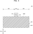
- FIG. 4 is a cross-sectional view illustrating an optical waveguide device according to a first reference example.
- the optical waveguide substrate 100 includes a substrate 110X, as illustrated in FIG. 4 .
- the material of the substrate 110X is the same as the material of the substrate 110.
- the other components are similar to those of the first embodiment.
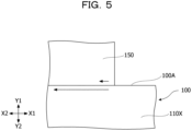
- FIG. 5 is a diagram illustrating deformation of the optical waveguide substrate and the optical waveguide layer in the first reference example.
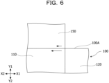
- FIG. 6 is a diagram illustrating deformation of the optical waveguide substrate and the optical waveguide layer in the first embodiment. Arrows in FIGs. 5 and 6 schematically illustrate the magnitudes of deformation, and the longer an arrow, the larger the deformation.
- the optical waveguide layer 150 and the stress relieving members 120 are formed with diamond, and the substrates 110 and 110X are sapphire substrates. Also, it is assumed that the dimension of the optical waveguide layer 150 in the X1-X2 direction is 0.2 ⁇ m, the dimension of the optical waveguide substrate 100 in the X1-X2 direction is 5.0 mm, and the optical waveguide layer 150 is disposed at the center of the optical waveguide substrate 100 in the X1-X2 direction.
- the entire first surface 100A is formed with the substrate 110X. Therefore, when cooled to 4 K from room temperature, the optical waveguide layer 150 has a thermal contraction amount of only 0.05 nm, while the first surface 100A has a thermal contraction amount of 12 ⁇ m, which means that the first surface 100A is thermally contracted by an amount 240,000 times that of the optical waveguide layer 150. Therefore, as illustrated in FIG. 5 , a large difference in thermal deformation occurs in the vicinity of the interface between the optical waveguide layer 150 and the optical waveguide substrate 100, and, in particular, stress concentrates in the vicinity of the end portions of the optical waveguide layer 150 in the X1-X2 direction.
- the portion of the first surface 100A in the first region 101 is formed with the substrate 110, but the portions of the first surface 100A in the second regions 102 are formed with the stress relieving members 120. Therefore, even if cooling from room temperature to 4 K is performed, only the portion of the first surface 100A in the first region 101 is thermally contracted greater than the optical waveguide layer 150. Accordingly, the difference in thermal deformation caused in the vicinity of the interface between the optical waveguide layer 150 and the optical waveguide substrate 100 is small, as illustrated in FIG. 6 .
- the first embodiment it is possible to reduce separation between the optical waveguide substrate 100 and the optical waveguide layer 150, compared with the first reference example.
- FIG. 7 is a cross-sectional view illustrating an optical waveguide device according to the second reference example.
- FIG. 8 is a cross-sectional view illustrating an optical waveguide device according to the third reference example.
- the optical waveguide substrate 100 includes only the substrate 110, and the optical waveguide substrate 100 does not include the stress relieving members 120, as illustrated in FIG. 7 .
- the other components are similar to those of the first embodiment.
- the optical waveguide substrate 100 includes a substrate 110X and a diamond layer 120Z, as illustrated in FIG. 8 .
- the diamond layer 120Z is disposed on substrate 110X, and the entire first surface 100A is formed with the diamond layer 120Z.
- the optical waveguide layer 150 and the diamond layer 120Z are integrally formed.
- the other components are similar to those of the first embodiment.
- FIGs. 9 to 12 are cross-sectional views illustrating a first method for manufacturing the optical waveguide device 1 according to the first embodiment.
- FIGs. 13 to 17 are cross-sectional views illustrating a second method for manufacturing the optical waveguide device 1 according to the first embodiment.
- a substrate that is flat on the Y1 side is first prepared, and this substrate is processed, to obtain the substrate 110 including the protruding portion 111 and the recessed portions 112.
- etching is performed, for example.
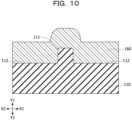
- a diamond layer 160 that will later be the optical waveguide layer 150 and the stress relieving members 120 is formed on substrate 110, with a greater thickness than the height of protruding portion 111.
- the diamond layer 160 may be formed by a chemical vapor deposition (CVD) method or the like, for example.
- the optical waveguide layer 150 including the color center 151 is disposed on the protruding portion 111, and the optical waveguide layer 150 and the substrate 110 are joined to each other.
- the optical waveguide layer 150 and the substrate 110 may be joined by an intermolecular force.
- the optical waveguide device 1 according to the first embodiment may be manufactured.
- the processes up to the formation of the diamond layer 160 are first performed as with the first manufacturing method (see FIG. 10 ).
- a mask 171 is formed on the region of the diamond layer 160 to be the optical waveguide layer 150.
- a resist pattern is formed, for example.
- the portions of the diamond layer 160 exposed through the mask 171 are subjected to dry etching, to form the stress relieving members 120 from the diamond layer 160.
- the optical waveguide substrate 100 having the first surface 100A is obtained.
- the optical waveguide substrate 100 includes the substrate 110 and the stress relieving members 120.
- the surface of the substrate 110 on the Y1 side and the surfaces of the stress relieving members 120 on the Y1 side are flush with each other, and are included in the first surface 100A.
- the portion of the diamond layer 160 exposed through the mask 172 is subjected to dry etching, to form the optical waveguide layer 150 from the diamond layer 160.
- the mask 172 is removed.
- the color center 151 is formed in the optical waveguide layer 150 by ion implantation or the like.
- the optical waveguide device 1 according to the first embodiment may be manufactured.
- FIG. 18 is a top view illustrating an optical waveguide device according to the second embodiment.
- FIG. 19 is a cross-sectional view illustrating the optical waveguide device according to the second embodiment.
- the optical waveguide substrate 200 includes a substrate 210 and stress relieving members 220.
- the thermal expansion coefficient of the substrate 210 is greater than the thermal expansion coefficient of the optical waveguide layer 150. Meanwhile, the thermal expansion coefficient of the stress relieving members 220 is smaller than the thermal expansion coefficient of the substrate 210.
- the substrate 210 contains sapphire, for example.
- the substrate 210 may be a sapphire substrate.
- the stress relieving members 220 contain diamond, for example.
- the stress relieving members 220 may be diamond members.
- the substrate 210 includes the first region 101 and the second regions 102, a protruding portion 211 is formed in the first region 101, and a plurality of recessed portions 212 is formed in the second regions 102.
- the plurality of recessed portions 212 is arranged in a square lattice-like shape in a planar view.
- the shape of the recessed portions 212 a cylindrical shape.
- the cross-sectional shape of the recessed portions 212 is a rectangular shape.
- the stress relieving members 220 are provided in the respective recessed portions 212.
- the surface of the protruding portion 211 on the Y1 side and the surfaces of the stress relieving members 220 on the Y1 side are flush with each other, and these surfaces constitute the first surface 200A.
- the first surface 200A includes the surface of the protruding portion 211 on the Y1 side, and the surfaces of the stress relieving members 220 on the Y1 side.
- the depth of the protruding portion 211 and the depth of the recessed portions 212 are about 100 nm to 1000 nm, for example.
- the other components are similar to those of the first embodiment.
- the second regions 102 function as photonic crystals.
- the shape of the recessed portions 212 is a cylindrical shape about 50 nm to 500 nm in diameter and about 100 nm to 1000 nm in depth, and the cycles of the recessed portions 212 in the X1-X2 direction and the Z1-Z2 direction are about 100 nm to 500 nm, for example.
- the optical waveguide device 2 according to the second embodiment may be manufactured by a method similar to that of the first embodiment.
- FIG. 20 is a top view illustrating an optical waveguide device according to a modification of the second embodiment.
- the stress relieving members 220 may not be provided in those located on the Z1 side of the optical waveguide layer 150, and those located on the Z2 side of the optical waveguide layer 150 but on the inner side compared with the optical waveguide layer 150.
- FIG. 21 is a cross-sectional view illustrating an optical waveguide device according to the third embodiment.
- recessed portions 312 instead of the recessed portions 212, are formed in the substrate 210.
- the shape of the recessed portions 312 is a conical tubular shape having diameter that is smaller at a portion closer to the Y2 side.
- the cross-sectional shape of the recessed portions 312 is a triangular shape.
- the stress relieving members 220 are provided in the respective recessed portions 312.
- the other components are similar to those of the second embodiment.
- the optical waveguide device 3 according to the third embodiment may also be manufactured by a method similar to that of the first embodiment.
- FIG. 22 is a cross-sectional view illustrating an optical waveguide device according to the fourth embodiment.
- recessed portions 412 instead of the recessed portions 212, are formed in the substrate 210.
- the shape of the recessed portions 412 is an isosceles trapezoidal conical tubular shape having diameter that is smaller at a portion closer to the Y2 side.
- the cross-sectional shape of the recessed portions 412 is an isosceles trapezoidal shape.
- the stress relieving members 220 are provided in the respective recessed portions 412.
- the other components are similar to those of the second embodiment.
- the optical waveguide device 4 according to the fourth embodiment may also be manufactured by a method similar to that of the first embodiment.
- the widths (dimensions in the X1-X2 direction) of the protruding portions 111 and 211 are not necessarily equal to the width (dimension in the X1-X2 direction) of the optical waveguide layer 150.
- the widths of the protruding portions 111 and 211 may be 150% or less of the width dimension of the optical waveguide layer 150.
- the widths of the protruding portions 111 and 211 are preferably 130% or less, more preferably 120% or less, and yet more preferably 110% or less of the width of the optical waveguide layer 150.
- the widths of the protruding portions 111 and 211 may be 70% or more of the width of the optical waveguide layer 150.
- the widths of the protruding portions 111 and 211 are preferably 75% or more, more preferably 80% or more, and yet more preferably 85% or more of the width of the optical waveguide layer 150.
- the materials of the substrate and the stress relieving members are not limited to any particular materials.
- the material of the substrate is sapphire, diamond, silicon nitride (Si 3 N 4 ), silicon carbide (SiC), or aluminum nitride (AIN) may be used as the material of the stress relieving members.
- the material of the substrate is silicon carbide
- diamond or silicon nitride may be used as the material of the stress relieving members.
- the thermal expansion coefficient of silicon nitride is 2.8 ⁇ 10 -6 /K
- the thermal expansion coefficient of silicon carbide is 3.7 ⁇ 10 -6 /K
- the thermal expansion coefficient of aluminum nitride is 4.6 ⁇ 10 -6 /K.
- the optical waveguide substrate may have a plurality of first regions, and a plurality of optical waveguide layers may be disposed on the optical waveguide substrate.
- FIG. 23 is a top view illustrating an optical waveguide device according to the fifth embodiment.
- an optical waveguide device 5 includes an optical waveguide substrate 500, instead of the optical waveguide substrate 100.
- the optical waveguide substrate 500 includes a substrate 510 and stress relieving members 520.
- the thermal expansion coefficient of the substrate 510 is greater than the thermal expansion coefficient of the optical waveguide layer 150. Meanwhile, the thermal expansion coefficient of the stress relieving members 520 is smaller than the thermal expansion coefficient of the substrate 510.
- the substrate 510 contains sapphire, for example.
- the substrate 510 may be a sapphire substrate.
- the stress relieving members 520 contain diamond, for example.
- the stress relieving members 520 may be diamond members.
- the substrate 510 includes a first region 101 and second regions 102, a protruding portion 511 is formed in the first region 101, and recessed portions 512 and recessed portions 212 are formed in the second regions 102.
- the recessed portions 512 are formed on the X1 side and the X2 side of the optical waveguide layer 150.
- the recessed portions 212 are formed on the Z1 side and the Z2 side of the recessed portions 512.
- the stress relieving members 520 are provided in the respective recessed portions 512.
- the stress relieving members 520 may also be provided in the recessed portions 212, and the stress relieving members 520 may not be provided in the recessed portions 212.
- the other components are similar to those of the first embodiment.
- the fifth embodiment it is also possible to reduce separation between the optical waveguide substrate 500 and the optical waveguide layer 150, as in the first embodiment.
- FIG. 24 is a top view illustrating an optical waveguide device according to the sixth embodiment.
- an optical waveguide device 6 includes an optical waveguide substrate 600, instead of the optical waveguide substrate 100.
- the optical waveguide substrate 600 includes a substrate 610 and stress relieving members 620.
- the thermal expansion coefficient of the substrate 610 is greater than the thermal expansion coefficient of the optical waveguide layer 150. Meanwhile, the thermal expansion coefficient of the stress relieving members 620 is smaller than the thermal expansion coefficient of the substrate 610.
- the substrate 610 contains sapphire, for example.
- the substrate 610 may be a sapphire substrate.
- the stress relieving members 620 contain diamond, for example.
- the stress relieving members 620 may be diamond members.
- the substrate 610 includes a first region 101 and second regions 102, a protruding portion 611 is formed in the first region 101, and recessed portions 612 and recessed portions 212 are formed in the second regions 102.
- the recessed portions 612 are formed on the X1 side and the X2 side of the optical waveguide layer 150.
- the recessed portions 612 have a rectangular planar shape extending in the Z1-Z2 direction in a planar view, and are arranged side by side in the X1-X2 direction.
- the recessed portions 212 are formed on the Z1 side and the Z2 side of the recessed portions 612.
- the stress relieving members 620 are provided in the respective recessed portions 612.
- the stress relieving members 620 may also be provided in the recessed portions 212, and the stress relieving members 620 may not be provided in the recessed portions 212.
- the other components are similar to those of the first embodiment.
- the sixth embodiment it is also possible to reduce separation between the optical waveguide substrate 600 and the optical waveguide layer 150, as in the first embodiment.
- FIG. 25 is a top view illustrating an optical waveguide device according to the seventh embodiment.
- an optical waveguide device 7 includes an optical waveguide substrate 700, instead of the optical waveguide substrate 200.
- the optical waveguide substrate 700 includes a substrate 710 and stress relieving members 220.
- the thermal expansion coefficient of the substrate 710 is greater than the thermal expansion coefficient of the optical waveguide layer 150. Meanwhile, the thermal expansion coefficient of the stress relieving members 220 is smaller than the thermal expansion coefficient of the substrate 710.
- the substrate 710 contains sapphire, for example.
- the substrate 710 may be a sapphire substrate.
- the stress relieving members 220 contain diamond, for example.
- the stress relieving members 220 may be diamond members.
- the substrate 710 includes a first region 101 and second regions 102, a protruding portion 711 is formed in the first region 101, and recessed portions 212 are formed in the second regions 102.
- the recessed portions 212 are formed on the X1 side and the X2 side of the optical waveguide layer 150.
- the stress relieving members 220 are provided in the respective recessed portions 212.
- the protruding portion 711 may also be formed in a region on the Z1 side of the optical waveguide layer 150, and in a region on the Z2 side of the optical waveguide layer 150. In this case, the refractive index of the protruding portion 711 is made to vary between the first region 101 and the second regions 102, for example, so that light can be confined in the first region 101.
- the other components are similar to those of the second embodiment.
- the seventh embodiment it is also possible to reduce separation between the optical waveguide substrate 700 and the optical waveguide layer 150, as in the first embodiment.
- the recessed portions 312 or the recessed portions 412 may be formed, instead of the recessed portions 212.
- FIG. 26 is a top view illustrating an optical waveguide device according to the eighth embodiment.
- an optical waveguide device 8 includes an optical waveguide substrate 800, instead of the optical waveguide substrate 500.
- the optical waveguide substrate 800 includes a substrate 810 and stress relieving members 520.
- the thermal expansion coefficient of the substrate 810 is greater than the thermal expansion coefficient of the optical waveguide layer 150. Meanwhile, the thermal expansion coefficient of the stress relieving members 520 is smaller than the thermal expansion coefficient of the substrate 810.
- the substrate 810 contains sapphire, for example.
- the substrate 810 may be a sapphire substrate.
- the stress relieving members 520 contain diamond, for example.
- the stress relieving members 520 may be diamond members.
- the substrate 810 includes a first region 101 and second regions 102, a protruding portion 811 is formed in the first region 101, and recessed portions 512 are formed in the second regions 102.
- the recessed portions 512 are formed on the X1 side and the X2 side of the optical waveguide layer 150.
- the stress relieving members 520 are provided in the respective recessed portions 512.
- the protruding portion 811 may also be formed in a region on the Z1 side of the optical waveguide layer 150, and in a region on the Z2 side of the optical waveguide layer 150. In this case, the refractive index of the protruding portion 811 is made to vary between the first region 101 and the second regions 102, for example, so that light can be confined in the first region 101.
- the eighth embodiment it is also possible to reduce separation between the optical waveguide substrate 800 and the optical waveguide layer 150, as in the first embodiment.
- FIG. 27 is a top view illustrating an optical waveguide device according to the ninth embodiment.
- an optical waveguide device 9 includes an optical waveguide substrate 900, instead of the optical waveguide substrate 600.
- the optical waveguide substrate 900 includes a substrate 910 and stress relieving members 620.
- the thermal expansion coefficient of the substrate 910 is greater than the thermal expansion coefficient of the optical waveguide layer 150. Meanwhile, the thermal expansion coefficient of the stress relieving members 620 is smaller than the thermal expansion coefficient of the substrate 910.
- the substrate 910 contains sapphire, for example.
- the substrate 910 may be a sapphire substrate.
- the stress relieving members 620 contain diamond, for example.
- the stress relieving members 620 may be diamond members.
- the substrate 910 includes a first region 101 and second regions 102, a protruding portion 911 is formed in the first region 101, and recessed portions 612 are formed in the second regions 102.
- the recessed portions 612 are formed on the X1 side and the X2 side of the optical waveguide layer 150.
- the recessed portions 612 have a rectangular planar shape extending in the Z1-Z2 direction in a planar view, and are arranged side by side in the X1-X2 direction.
- the stress relieving members 620 are provided in the respective recessed portions 612.
- the protruding portion 911 may also be formed in a region on the Z1 side of the optical waveguide layer 150, and in a region on the Z2 side of the optical waveguide layer 150.
- the refractive index of the protruding portion 911 is made to vary between the first region 101 and the second regions 102, for example, so that light can be confined in the first region 101.
- the ninth embodiment it is also possible to reduce separation between the optical waveguide substrate 900 and the optical waveguide layer 150, as in the first embodiment.
- FIG. 28 is a diagram illustrating a quantum computer according to the tenth embodiment.
- a quantum computer 10 according to the tenth embodiment includes a general-purpose computer 1001, a control unit 1002, and a quantum device 1003.
- the control unit 1002 controls the quantum device 1003, based on a control signal from the general-purpose computer 1001.
- a quantum device including the optical waveguide device according to one of the first to ninth embodiments is used as the quantum device 1003.
- the control unit 1002 and the quantum device 1003 are housed in a cryostat 1004.
Landscapes
- Physics & Mathematics (AREA)
- Engineering & Computer Science (AREA)
- Microelectronics & Electronic Packaging (AREA)
- General Physics & Mathematics (AREA)
- Optics & Photonics (AREA)
- Optical Integrated Circuits (AREA)
Abstract
Description
- The present disclosure relates to an optical waveguide device, a quantum operation device, and a method for manufacturing the optical waveguide device.
- A quantum device using a color center in a diamond layer has been studied. Also, an optical waveguide device has been studied. In the optical waveguide device, an optical waveguide layer formed with diamond, and an optical waveguide substrate formed with a material such as sapphire having a lower refractive index than that of diamond are joined to each other, to propagate light emitted at a color center to a detector.
- In a conventional optical waveguide device, there is a possibility that separation occurs between the optical waveguide substrate and the optical waveguide layer.
- An object of the present disclosure is to provide an optical waveguide device that is capable of reducing separation between an optical waveguide substrate and an optical waveguide layer, a quantum operation device, and a method for manufacturing the optical waveguide device.
- According to one aspect of the present disclosure, there is provided an optical waveguide device that includes: an optical waveguide substrate that has a first surface; and an optical waveguide layer that is provided on the first surface. In the optical waveguide device, the optical waveguide substrate includes: a first region that is exposed on the first surface, and extends linearly; and a second region that is exposed on the first surface, and is located on both sides of the first region in a planar view. The optical waveguide layer is provided on the first region, a second thermal expansion coefficient of the second region is smaller than a first thermal expansion coefficient of the first region, and a third thermal expansion coefficient of the optical waveguide layer is smaller than the first thermal expansion coefficient.
- According to the present disclosure, it is possible to reduce separation between the optical waveguide substrate and the optical waveguide layer.
-
-
FIG. 1 is a perspective view illustrating an optical waveguide device according to a first embodiment. -
FIG. 2 is a cross-sectional view (part 1) illustrating the optical waveguide device according to the first embodiment. -
FIG. 3 is a cross-sectional view (part 2) illustrating the optical waveguide device according to the first embodiment. -
FIG. 4 is a cross-sectional view illustrating an optical waveguide device according to a first reference example. -
FIG. 5 is a diagram illustrating deformation of an optical waveguide substrate and an optical waveguide layer in the first reference example. -
FIG. 6 is a diagram illustrating deformation of an optical waveguide substrate and an optical waveguide layer in the first embodiment. -
FIG. 7 is a cross-sectional view illustrating an optical waveguide device according to a second reference example. -
FIG. 8 is a cross-sectional view illustrating an optical waveguide device according to a third reference example. -
FIG. 9 is a cross-sectional view (part 1) illustrating a first method for manufacturing the optical waveguide device according to the first embodiment. -
FIG. 10 is a cross-sectional view (part 2) illustrating the first method for manufacturing the optical waveguide device according to the first embodiment. -
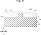
FIG. 11 is a cross-sectional view (part 3) illustrating the first method for manufacturing the optical waveguide device according to the first embodiment. -
FIG. 12 is a cross-sectional view (part 4) illustrating the first method for manufacturing the optical waveguide device according to the first embodiment. -
FIG. 13 is a cross-sectional view (part 1) illustrating a second method for manufacturing the optical waveguide device according to the first embodiment. -
FIG. 14 is a cross-sectional view (part 2) illustrating the second method for manufacturing the optical waveguide device according to the first embodiment. -
FIG. 15 is a cross-sectional view (part 3) illustrating the second method for manufacturing the optical waveguide device according to the first embodiment. -
FIG. 16 is a cross-sectional view (part 4) illustrating the second method for manufacturing the optical waveguide device according to the first embodiment. -
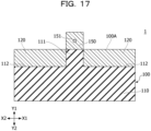
FIG. 17 is a cross-sectional view (part 5) illustrating the second method for manufacturing the optical waveguide device according to the first embodiment. -
FIG. 18 is a top view illustrating an optical waveguide device according to a second embodiment. -
FIG. 19 is a cross-sectional view illustrating the optical waveguide device according to the second embodiment. -
FIG. 20 is a top view illustrating an optical waveguide device according to a modification of the second embodiment. -
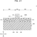
FIG. 21 is a cross-sectional view illustrating an optical waveguide device according to a third embodiment. -
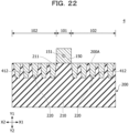
FIG. 22 is a cross-sectional view illustrating an optical waveguide device according to a fourth embodiment. -
FIG. 23 is a top view illustrating an optical waveguide device according to a fifth embodiment. -
FIG. 24 is a top view illustrating an optical waveguide device according to a sixth embodiment. -
FIG. 25 is a top view illustrating an optical waveguide device according to a seventh embodiment. -
FIG. 26 is a top view illustrating an optical waveguide device according to an eighth embodiment. -
FIG. 27 is a top view illustrating an optical waveguide device according to a ninth embodiment. -
FIG. 28 is a diagram illustrating a quantum computer according to a tenth embodiment. - In the description below, embodiments of the present disclosure will be specifically described with reference to the accompanying drawings. Note that, in the present specification and the drawings, components having substantially the same functional configurations are denoted by the same reference numerals, and repetitive explanation thereof will be omitted in some cases. In the present disclosure, it is assumed that an X1-X2 direction, a Y1-Y2 direction, and a Z1-Z2 direction are directions orthogonal to one another. A plane including the X1-X2 direction and the Y1-Y2 direction is referred to as an X-Y plane, a plane including the Y1-Y2 direction and the Z1-Z2 direction is referred to as a Y-Z plane, and a plane including the Z1-Z2 direction and the X1-X2 direction is referred to as a Z-X plane. Note that, for convenience sake, the Y1-Y2 direction is set as the vertical direction, and the Y1 side is set as the upper side, and the Y2 side is set as the lower side. Furthermore, a planar view means viewing an object from the Y1 side, and a planar shape means a shape of an object viewed from the Y1 side.
- First, a first embodiment is described. The first embodiment relates to an optical waveguide device. The optical waveguide device according to the first embodiment is used for a quantum operation device such as a quantum computer, for example.
FIG. 1 is a perspective view illustrating the optical waveguide device according to the first embodiment.FIGs. 2 and3 are cross-sectional view illustrating the optical waveguide device according to the first embodiment. - As illustrated in
FIGs. 1 to 3 , anoptical waveguide device 1 according to the first embodiment includes anoptical waveguide substrate 100 and anoptical waveguide layer 150. Theoptical waveguide substrate 100 has afirst surface 100A on the Y1 side. Thefirst surface 100A is parallel to the Z-X plane. Theoptical waveguide layer 150 is disposed on thefirst surface 100A. - The
optical waveguide substrate 100 has afirst region 101 andsecond regions 102. Thefirst region 101 and thesecond regions 102 are exposed on thefirst surface 100A. Thefirst region 101 extends linearly. Thefirst region 101 extends in parallel to the Z1-Z2 direction, for example. Thesecond regions 102 are located on both sides of thefirst region 101 in a planar view, which is when viewed from a direction perpendicular to thefirst surface 100A. That is, thefirst region 101 is interposed between the twosecond regions 102 in the X1-X2 direction. Theoptical waveguide layer 150 is disposed over thefirst region 101. - The
optical waveguide substrate 100 includes asubstrate 110 andstress relieving members 120. The thermal expansion coefficient of thesubstrate 110 is greater than the thermal expansion coefficient of theoptical waveguide layer 150. Meanwhile, the thermal expansion coefficient of thestress relieving members 120 is smaller than the thermal expansion coefficient of thesubstrate 110. Theoptical waveguide layer 150 contains diamond, for example. Theoptical waveguide layer 150 may be a diamond layer. Thesubstrate 110 contains sapphire (Al2O3), for example. Thesubstrate 110 may be a sapphire substrate. Thestress relieving members 120 contain diamond, for example. Thestress relieving members 120 may be diamond members. The thermal expansion coefficient of diamond is 0.8 × 10⁻⁶/K, and the thermal expansion coefficient of sapphire is 8.0 × 10⁻⁶/K. - The
substrate 110 includes thefirst region 101 and thesecond regions 102, a protrudingportion 111 is formed in thefirst region 101, and recessedportions 112 are formed in thesecond regions 102. Thestress relieving members 120 are provided in the respective recessedportions 112. The surface of the protrudingportion 111 on the Y1 side and the surfaces of thestress relieving members 120 on the Y1 side are flush with each other, and these surfaces constitute thefirst surface 100A. That is, thefirst surface 100A includes the surface of the protrudingportion 111 on the Y1 side, and the surfaces of thestress relieving members 120 on the Y1 side. The depth of the protrudingportion 111 and the depth of the recessedportions 112 are about 100 nm to 1000 nm, for example. - In the
optical waveguide substrate 100, thefirst region 101 functions as an optical waveguide. For example, the refractive index of the portion that functions as an optical waveguide in theoptical waveguide substrate 100 is lower than the refractive index of theoptical waveguide layer 150. - The
optical waveguide layer 150 includes acolor center 151, for example. The end portion of theoptical waveguide layer 150 closer to the side of a detector (not illustrated) than thecolor center 151, which is the Z1 side in the present embodiment, may be in a shape having a height that is smaller at a portion closer to the tip. In this case, a high light propagation efficiency is likely to be achieved between theoptical waveguide layer 150 and thefirst region 101 of theoptical waveguide substrate 100. - The
optical waveguide device 1 according to the first embodiment is cooled to a cryogenic temperature of 4 K or lower, for example, and is then used. Therefore, theoptical waveguide substrate 100 and theoptical waveguide layer 150 are thermally contracted during use, and are thermally expanded when returned to room temperature after use. In the present embodiment, the protrudingportion 111 and the recessedportions 112 are formed on thesubstrate 110, and thestress relieving members 120 are provided in the recessedportions 112. Accordingly, the thermal expansion coefficient of thesecond regions 102 is smaller than the thermal expansion coefficient of thefirst region 101. Also, the thermal expansion coefficient of theoptical waveguide layer 150 is smaller than the thermal expansion coefficient of thefirst region 101. Because of this, the difference between the thermal expansion coefficient of thesecond regions 102 and the thermal expansion coefficient of theoptical waveguide layer 150 can be made smaller than the difference between the thermal expansion coefficient of thefirst region 101 and the thermal expansion coefficient of theoptical waveguide layer 150, and the stress to be generated between the entireoptical waveguide substrate 100 and theoptical waveguide layer 150 can be reduced. Thus, separation between theoptical waveguide substrate 100 and theoptical waveguide layer 150 can be reduced. - Here, the effects of the first embodiment are further described, while being compared with those of reference examples.
FIG. 4 is a cross-sectional view illustrating an optical waveguide device according to a first reference example. - In an
optical waveguide device 1X according to the first reference example, theoptical waveguide substrate 100 includes asubstrate 110X, as illustrated inFIG. 4 . The material of thesubstrate 110X is the same as the material of thesubstrate 110. The other components are similar to those of the first embodiment. -
FIG. 5 is a diagram illustrating deformation of the optical waveguide substrate and the optical waveguide layer in the first reference example.FIG. 6 is a diagram illustrating deformation of the optical waveguide substrate and the optical waveguide layer in the first embodiment. Arrows inFIGs. 5 and6 schematically illustrate the magnitudes of deformation, and the longer an arrow, the larger the deformation. - For example, it is assumed that the
optical waveguide layer 150 and thestress relieving members 120 are formed with diamond, and thesubstrates optical waveguide layer 150 in the X1-X2 direction is 0.2 µm, the dimension of theoptical waveguide substrate 100 in the X1-X2 direction is 5.0 mm, and theoptical waveguide layer 150 is disposed at the center of theoptical waveguide substrate 100 in the X1-X2 direction. - In the first reference example, the entire
first surface 100A is formed with thesubstrate 110X. Therefore, when cooled to 4 K from room temperature, theoptical waveguide layer 150 has a thermal contraction amount of only 0.05 nm, while thefirst surface 100A has a thermal contraction amount of 12 µm, which means that thefirst surface 100A is thermally contracted by an amount 240,000 times that of theoptical waveguide layer 150. Therefore, as illustrated inFIG. 5 , a large difference in thermal deformation occurs in the vicinity of the interface between theoptical waveguide layer 150 and theoptical waveguide substrate 100, and, in particular, stress concentrates in the vicinity of the end portions of theoptical waveguide layer 150 in the X1-X2 direction. - In the first embodiment, on the other hand, the portion of the
first surface 100A in thefirst region 101 is formed with thesubstrate 110, but the portions of thefirst surface 100A in thesecond regions 102 are formed with thestress relieving members 120. Therefore, even if cooling from room temperature to 4 K is performed, only the portion of thefirst surface 100A in thefirst region 101 is thermally contracted greater than theoptical waveguide layer 150. Accordingly, the difference in thermal deformation caused in the vicinity of the interface between theoptical waveguide layer 150 and theoptical waveguide substrate 100 is small, as illustrated inFIG. 6 . - Thus, according to the first embodiment, it is possible to reduce separation between the
optical waveguide substrate 100 and theoptical waveguide layer 150, compared with the first reference example. - Next, a second reference example and a third reference example are described.
FIG. 7 is a cross-sectional view illustrating an optical waveguide device according to the second reference example.FIG. 8 is a cross-sectional view illustrating an optical waveguide device according to the third reference example. - In an
optical waveguide device 1Y according to the second reference example, theoptical waveguide substrate 100 includes only thesubstrate 110, and theoptical waveguide substrate 100 does not include thestress relieving members 120, as illustrated inFIG. 7 . The other components are similar to those of the first embodiment. - According to such a second reference example, it is possible to reduce separation between the
optical waveguide substrate 100 and theoptical waveguide layer 150, as in the first embodiment. However, since thestress relieving members 120 are not provided, a large stress concentrates in the vicinity of thebase 113Y of the protrudingportion 111 with a temperature change, and there is a possibility that a defect such as a crack might appear in thesubstrate 110. - In an
optical waveguide device 1Z according to the third reference example, theoptical waveguide substrate 100 includes asubstrate 110X and adiamond layer 120Z, as illustrated inFIG. 8 . Thediamond layer 120Z is disposed onsubstrate 110X, and the entirefirst surface 100A is formed with thediamond layer 120Z. Theoptical waveguide layer 150 and thediamond layer 120Z are integrally formed. The other components are similar to those of the first embodiment. - According to such a third reference example, it is possible to suppress separation between the integrally formed
optical waveguide layer 150 anddiamond layer 120Z, and thesubstrate 110X. However, a large stress concentrates in the vicinity of thebase 113Z of theoptical waveguide layer 150, and there is a possibility that a defect such as a crack might appear in thediamond layer 120Z. Furthermore, since thediamond layer 120Z is provided, the optical confinement effect is degraded, and a coupling loss is caused in the optical coupling between theoptical waveguide layer 150 and the optical waveguide included in theoptical waveguide substrate 100. - Next, two types of methods for manufacturing the
optical waveguide device 1 according to the first embodiment are described.FIGs. 9 to 12 are cross-sectional views illustrating a first method for manufacturing theoptical waveguide device 1 according to the first embodiment.FIGs. 13 to 17 are cross-sectional views illustrating a second method for manufacturing theoptical waveguide device 1 according to the first embodiment. - By the first manufacturing method, as illustrated in
FIG. 9 , a substrate that is flat on the Y1 side is first prepared, and this substrate is processed, to obtain thesubstrate 110 including the protrudingportion 111 and the recessedportions 112. For the processing of the substrate, etching is performed, for example. - Next, as illustrated in
FIG. 10 , adiamond layer 160 that will later be theoptical waveguide layer 150 and thestress relieving members 120 is formed onsubstrate 110, with a greater thickness than the height of protrudingportion 111. Thediamond layer 160 may be formed by a chemical vapor deposition (CVD) method or the like, for example. - After that, as illustrated in
FIG. 11 , thediamond layer 160 is polished until the protrudingportion 111 is exposed. As a result, theoptical waveguide substrate 100 having thefirst surface 100A is obtained. Theoptical waveguide substrate 100 includes thesubstrate 110 and thestress relieving members 120. The surface of thesubstrate 110 on the Y1 side and the surfaces of thestress relieving members 120 on the Y1 side are flush with each other, and are included in thefirst surface 100A. - Subsequently, as illustrated in
FIG. 12 , theoptical waveguide layer 150 including thecolor center 151 is disposed on the protrudingportion 111, and theoptical waveguide layer 150 and thesubstrate 110 are joined to each other. For example, theoptical waveguide layer 150 and thesubstrate 110 may be joined by an intermolecular force. - In this manner, the
optical waveguide device 1 according to the first embodiment may be manufactured. - By the second manufacturing method, the processes up to the formation of the
diamond layer 160 are first performed as with the first manufacturing method (seeFIG. 10 ). Next, as illustrated inFIG. 13 , amask 171 is formed on the region of thediamond layer 160 to be theoptical waveguide layer 150. As themask 171, a resist pattern is formed, for example. - After that, as illustrated in
FIG. 14 , the portions of thediamond layer 160 exposed through themask 171 are subjected to dry etching, to form thestress relieving members 120 from thediamond layer 160. As a result, theoptical waveguide substrate 100 having thefirst surface 100A is obtained. Theoptical waveguide substrate 100 includes thesubstrate 110 and thestress relieving members 120. The surface of thesubstrate 110 on the Y1 side and the surfaces of thestress relieving members 120 on the Y1 side are flush with each other, and are included in thefirst surface 100A. - Subsequently, as illustrated in
FIG. 15 , themask 171 is removed. Next, amask 172 that covers the surfaces of thestress relieving members 120 on the Y1 side and exposes the surface of thediamond layer 160 on the Y1 side is formed on thestress relieving members 120. It is assumed that the thickness of themask 172 is about the same as the thickness of theoptical waveguide layer 150 to be formed. As themask 172, a resist pattern is formed, for example. As themask 172, a hard mask of silicon oxide (SiO2), silicon nitride (SiN), or metal may be formed. - After that, as illustrated in
FIG. 16 , the portion of thediamond layer 160 exposed through themask 172 is subjected to dry etching, to form theoptical waveguide layer 150 from thediamond layer 160. - Subsequently, as illustrated in
FIG. 17 , themask 172 is removed. Next, thecolor center 151 is formed in theoptical waveguide layer 150 by ion implantation or the like. - In this manner, the
optical waveguide device 1 according to the first embodiment may be manufactured. - Next, a second embodiment is described. The second embodiment differs from the first embodiment mainly in the configuration of the optical waveguide substrate.
FIG. 18 is a top view illustrating an optical waveguide device according to the second embodiment.FIG. 19 is a cross-sectional view illustrating the optical waveguide device according to the second embodiment. - As illustrated in
FIGs. 18 and19 , anoptical waveguide device 2 according to the second embodiment includes anoptical waveguide substrate 200, instead of theoptical waveguide substrate 100. Theoptical waveguide substrate 200 has afirst surface 200A on the Y1 side. Thefirst surface 200A is parallel to the Z-X plane. Theoptical waveguide layer 150 is disposed on thefirst surface 200A. Thefirst region 101 and thesecond regions 102 of theoptical waveguide substrate 200 are exposed on thefirst surface 200A. - The
optical waveguide substrate 200 includes asubstrate 210 andstress relieving members 220. The thermal expansion coefficient of thesubstrate 210 is greater than the thermal expansion coefficient of theoptical waveguide layer 150. Meanwhile, the thermal expansion coefficient of thestress relieving members 220 is smaller than the thermal expansion coefficient of thesubstrate 210. Thesubstrate 210 contains sapphire, for example. Thesubstrate 210 may be a sapphire substrate. Thestress relieving members 220 contain diamond, for example. Thestress relieving members 220 may be diamond members. - The
substrate 210 includes thefirst region 101 and thesecond regions 102, a protrudingportion 211 is formed in thefirst region 101, and a plurality of recessedportions 212 is formed in thesecond regions 102. The plurality of recessedportions 212 is arranged in a square lattice-like shape in a planar view. The shape of the recessed portions 212 a cylindrical shape. The cross-sectional shape of the recessedportions 212 is a rectangular shape. Thestress relieving members 220 are provided in the respective recessedportions 212. The surface of the protrudingportion 211 on the Y1 side and the surfaces of thestress relieving members 220 on the Y1 side are flush with each other, and these surfaces constitute thefirst surface 200A. That is, thefirst surface 200A includes the surface of the protrudingportion 211 on the Y1 side, and the surfaces of thestress relieving members 220 on the Y1 side. The depth of the protrudingportion 211 and the depth of the recessedportions 212 are about 100 nm to 1000 nm, for example. - The other components are similar to those of the first embodiment.
- According to the second embodiment, it is also possible to reduce separation between the
optical waveguide substrate 200 and theoptical waveguide layer 150, as in the first embodiment. - Also, in the second embodiment, depending on the layout of the plurality of recessed
portions 212 and thestress relieving members 220, thesecond regions 102 function as photonic crystals. In a case where thesecond regions 102 function as photonic crystals, the shape of the recessedportions 212 is a cylindrical shape about 50 nm to 500 nm in diameter and about 100 nm to 1000 nm in depth, and the cycles of the recessedportions 212 in the X1-X2 direction and the Z1-Z2 direction are about 100 nm to 500 nm, for example. - The
optical waveguide device 2 according to the second embodiment may be manufactured by a method similar to that of the first embodiment. - Note that, as illustrated in
FIG. 20 , a plurality of recessedportions 212 may be arranged in a triangular lattice-like shape in a planar view, and thestress relieving members 220 may be provided in the respective recessedportions 212.FIG. 20 is a top view illustrating an optical waveguide device according to a modification of the second embodiment. - Further, among the plurality of recessed
portions 212, thestress relieving members 220 may not be provided in those located on the Z1 side of theoptical waveguide layer 150, and those located on the Z2 side of theoptical waveguide layer 150 but on the inner side compared with theoptical waveguide layer 150. - Next, a third embodiment is described. The third embodiment differs from the second embodiment mainly in the cross-sectional shape of the recessed portions.
FIG. 21 is a cross-sectional view illustrating an optical waveguide device according to the third embodiment. - As illustrated in
FIG. 21 , in anoptical waveguide device 3 according to the third embodiment, recessedportions 312, instead of the recessedportions 212, are formed in thesubstrate 210. The shape of the recessedportions 312 is a conical tubular shape having diameter that is smaller at a portion closer to the Y2 side. The cross-sectional shape of the recessedportions 312 is a triangular shape. Thestress relieving members 220 are provided in the respective recessedportions 312. - The other components are similar to those of the second embodiment.
- Effects similar to those of the second embodiment may also be achieved with the third embodiment.
- The
optical waveguide device 3 according to the third embodiment may also be manufactured by a method similar to that of the first embodiment. - Next, a fourth embodiment is described. The fourth embodiment differs from the second embodiment mainly in the cross-sectional shape of the recessed portions.
FIG. 22 is a cross-sectional view illustrating an optical waveguide device according to the fourth embodiment. - As illustrated in
FIG. 22 , in anoptical waveguide device 4 according to the fourth embodiment, recessedportions 412, instead of the recessedportions 212, are formed in thesubstrate 210. The shape of the recessedportions 412 is an isosceles trapezoidal conical tubular shape having diameter that is smaller at a portion closer to the Y2 side. The cross-sectional shape of the recessedportions 412 is an isosceles trapezoidal shape. Thestress relieving members 220 are provided in the respective recessedportions 412. - The other components are similar to those of the second embodiment.
- Effects similar to those of the second embodiment may also be achieved with the fourth embodiment.
- The
optical waveguide device 4 according to the fourth embodiment may also be manufactured by a method similar to that of the first embodiment. - The widths (dimensions in the X1-X2 direction) of the protruding
portions optical waveguide layer 150. For example, the widths of the protrudingportions optical waveguide layer 150. The widths of the protrudingportions optical waveguide layer 150. Also, the widths of the protrudingportions optical waveguide layer 150. The widths of the protrudingportions optical waveguide layer 150. - Note that, in the present disclosure, the materials of the substrate and the stress relieving members are not limited to any particular materials. For example, in a case where the material of the substrate is sapphire, diamond, silicon nitride (Si3N4), silicon carbide (SiC), or aluminum nitride (AIN) may be used as the material of the stress relieving members. Also, in a case where the material of the substrate is silicon carbide, diamond or silicon nitride may be used as the material of the stress relieving members. The thermal expansion coefficient of silicon nitride is 2.8 × 10⁻⁶/K, the thermal expansion coefficient of silicon carbide is 3.7 × 10⁻⁶/K, and the thermal expansion coefficient of aluminum nitride is 4.6 × 10⁻⁶/K.
- Further, the optical waveguide substrate may have a plurality of first regions, and a plurality of optical waveguide layers may be disposed on the optical waveguide substrate.
- Next, a fifth embodiment is described. The fifth embodiment differs from the first embodiment and the like mainly in the configuration of the substrate.
FIG. 23 is a top view illustrating an optical waveguide device according to the fifth embodiment. - As illustrated in
FIG. 23 , anoptical waveguide device 5 according to the fifth embodiment includes anoptical waveguide substrate 500, instead of theoptical waveguide substrate 100. Theoptical waveguide substrate 500 includes asubstrate 510 andstress relieving members 520. The thermal expansion coefficient of thesubstrate 510 is greater than the thermal expansion coefficient of theoptical waveguide layer 150. Meanwhile, the thermal expansion coefficient of thestress relieving members 520 is smaller than the thermal expansion coefficient of thesubstrate 510. Thesubstrate 510 contains sapphire, for example. Thesubstrate 510 may be a sapphire substrate. Thestress relieving members 520 contain diamond, for example. Thestress relieving members 520 may be diamond members. - The
substrate 510 includes afirst region 101 andsecond regions 102, a protrudingportion 511 is formed in thefirst region 101, and recessedportions 512 and recessedportions 212 are formed in thesecond regions 102. The recessedportions 512 are formed on the X1 side and the X2 side of theoptical waveguide layer 150. The recessedportions 212 are formed on the Z1 side and the Z2 side of the recessedportions 512. Thestress relieving members 520 are provided in the respective recessedportions 512. Thestress relieving members 520 may also be provided in the recessedportions 212, and thestress relieving members 520 may not be provided in the recessedportions 212. - The other components are similar to those of the first embodiment.
- According to the fifth embodiment, it is also possible to reduce separation between the
optical waveguide substrate 500 and theoptical waveguide layer 150, as in the first embodiment. - Next, a sixth embodiment is described. The sixth embodiment differs from the first embodiment and the like mainly in the configuration of the substrate.
FIG. 24 is a top view illustrating an optical waveguide device according to the sixth embodiment. - As illustrated in
FIG. 24 , anoptical waveguide device 6 according to the sixth embodiment includes anoptical waveguide substrate 600, instead of theoptical waveguide substrate 100. Theoptical waveguide substrate 600 includes asubstrate 610 andstress relieving members 620. The thermal expansion coefficient of thesubstrate 610 is greater than the thermal expansion coefficient of theoptical waveguide layer 150. Meanwhile, the thermal expansion coefficient of thestress relieving members 620 is smaller than the thermal expansion coefficient of thesubstrate 610. Thesubstrate 610 contains sapphire, for example. Thesubstrate 610 may be a sapphire substrate. Thestress relieving members 620 contain diamond, for example. Thestress relieving members 620 may be diamond members. - The
substrate 610 includes afirst region 101 andsecond regions 102, a protrudingportion 611 is formed in thefirst region 101, and recessedportions 612 and recessedportions 212 are formed in thesecond regions 102. The recessedportions 612 are formed on the X1 side and the X2 side of theoptical waveguide layer 150. The recessedportions 612 have a rectangular planar shape extending in the Z1-Z2 direction in a planar view, and are arranged side by side in the X1-X2 direction. The recessedportions 212 are formed on the Z1 side and the Z2 side of the recessedportions 612. Thestress relieving members 620 are provided in the respective recessedportions 612. Thestress relieving members 620 may also be provided in the recessedportions 212, and thestress relieving members 620 may not be provided in the recessedportions 212. - The other components are similar to those of the first embodiment.
- According to the sixth embodiment, it is also possible to reduce separation between the
optical waveguide substrate 600 and theoptical waveguide layer 150, as in the first embodiment. - Next, a seventh embodiment is described. The seventh embodiment differs from the second embodiment and the like mainly in the configuration of the substrate.
FIG. 25 is a top view illustrating an optical waveguide device according to the seventh embodiment. - As illustrated in
FIG. 25 , anoptical waveguide device 7 according to the seventh embodiment includes anoptical waveguide substrate 700, instead of theoptical waveguide substrate 200. Theoptical waveguide substrate 700 includes asubstrate 710 andstress relieving members 220. The thermal expansion coefficient of thesubstrate 710 is greater than the thermal expansion coefficient of theoptical waveguide layer 150. Meanwhile, the thermal expansion coefficient of thestress relieving members 220 is smaller than the thermal expansion coefficient of thesubstrate 710. Thesubstrate 710 contains sapphire, for example. Thesubstrate 710 may be a sapphire substrate. Thestress relieving members 220 contain diamond, for example. Thestress relieving members 220 may be diamond members. - The
substrate 710 includes afirst region 101 andsecond regions 102, a protrudingportion 711 is formed in thefirst region 101, and recessedportions 212 are formed in thesecond regions 102. The recessedportions 212 are formed on the X1 side and the X2 side of theoptical waveguide layer 150. Thestress relieving members 220 are provided in the respective recessedportions 212. In thesecond regions 102, the protrudingportion 711 may also be formed in a region on the Z1 side of theoptical waveguide layer 150, and in a region on the Z2 side of theoptical waveguide layer 150. In this case, the refractive index of the protrudingportion 711 is made to vary between thefirst region 101 and thesecond regions 102, for example, so that light can be confined in thefirst region 101. - The other components are similar to those of the second embodiment.
- According to the seventh embodiment, it is also possible to reduce separation between the
optical waveguide substrate 700 and theoptical waveguide layer 150, as in the first embodiment. - In the fifth to seventh embodiments, the recessed
portions 312 or the recessedportions 412 may be formed, instead of the recessedportions 212. - Next, an eighth embodiment is described. The eighth embodiment differs from the fifth embodiment and the like mainly in the configuration of the substrate.
FIG. 26 is a top view illustrating an optical waveguide device according to the eighth embodiment. - As illustrated in
FIG. 26 , anoptical waveguide device 8 according to the eighth embodiment includes anoptical waveguide substrate 800, instead of theoptical waveguide substrate 500. Theoptical waveguide substrate 800 includes asubstrate 810 andstress relieving members 520. The thermal expansion coefficient of thesubstrate 810 is greater than the thermal expansion coefficient of theoptical waveguide layer 150. Meanwhile, the thermal expansion coefficient of thestress relieving members 520 is smaller than the thermal expansion coefficient of thesubstrate 810. Thesubstrate 810 contains sapphire, for example. Thesubstrate 810 may be a sapphire substrate. Thestress relieving members 520 contain diamond, for example. Thestress relieving members 520 may be diamond members. - The
substrate 810 includes afirst region 101 andsecond regions 102, a protrudingportion 811 is formed in thefirst region 101, and recessedportions 512 are formed in thesecond regions 102. The recessedportions 512 are formed on the X1 side and the X2 side of theoptical waveguide layer 150. Thestress relieving members 520 are provided in the respective recessedportions 512. In thesecond regions 102, the protrudingportion 811 may also be formed in a region on the Z1 side of theoptical waveguide layer 150, and in a region on the Z2 side of theoptical waveguide layer 150. In this case, the refractive index of the protrudingportion 811 is made to vary between thefirst region 101 and thesecond regions 102, for example, so that light can be confined in thefirst region 101. - Other components are similar to those of the fifth embodiment.
- According to the eighth embodiment, it is also possible to reduce separation between the
optical waveguide substrate 800 and theoptical waveguide layer 150, as in the first embodiment. - Next, a ninth embodiment is described. The ninth embodiment differs from the sixth embodiment and the like mainly in the configuration of the substrate.
FIG. 27 is a top view illustrating an optical waveguide device according to the ninth embodiment. - As illustrated in
FIG. 27 , anoptical waveguide device 9 according to the ninth embodiment includes anoptical waveguide substrate 900, instead of theoptical waveguide substrate 600. Theoptical waveguide substrate 900 includes asubstrate 910 andstress relieving members 620. The thermal expansion coefficient of thesubstrate 910 is greater than the thermal expansion coefficient of theoptical waveguide layer 150. Meanwhile, the thermal expansion coefficient of thestress relieving members 620 is smaller than the thermal expansion coefficient of thesubstrate 910. Thesubstrate 910 contains sapphire, for example. Thesubstrate 910 may be a sapphire substrate. Thestress relieving members 620 contain diamond, for example. Thestress relieving members 620 may be diamond members. - The
substrate 910 includes afirst region 101 andsecond regions 102, a protrudingportion 911 is formed in thefirst region 101, and recessedportions 612 are formed in thesecond regions 102. The recessedportions 612 are formed on the X1 side and the X2 side of theoptical waveguide layer 150. The recessedportions 612 have a rectangular planar shape extending in the Z1-Z2 direction in a planar view, and are arranged side by side in the X1-X2 direction. Thestress relieving members 620 are provided in the respective recessedportions 612. In thesecond regions 102, the protrudingportion 911 may also be formed in a region on the Z1 side of theoptical waveguide layer 150, and in a region on the Z2 side of theoptical waveguide layer 150. In this case, the refractive index of the protrudingportion 911 is made to vary between thefirst region 101 and thesecond regions 102, for example, so that light can be confined in thefirst region 101. - Other components are similar to those of the sixth embodiment.
- According to the ninth embodiment, it is also possible to reduce separation between the
optical waveguide substrate 900 and theoptical waveguide layer 150, as in the first embodiment. - Next, a tenth embodiment is described. The tenth embodiment relates to a quantum computer.
FIG. 28 is a diagram illustrating a quantum computer according to the tenth embodiment. - A
quantum computer 10 according to the tenth embodiment includes a general-purpose computer 1001, acontrol unit 1002, and aquantum device 1003. Thecontrol unit 1002 controls thequantum device 1003, based on a control signal from the general-purpose computer 1001. A quantum device including the optical waveguide device according to one of the first to ninth embodiments is used as thequantum device 1003. Thecontrol unit 1002 and thequantum device 1003 are housed in acryostat 1004. - With the
quantum computer 10, it is possible to perform a stable quantum operation. - Although the preferred embodiments and the like have been described in detail so far, the present disclosure is not limited to the embodiments and the like described above, and various modifications and substitutions may be made to the embodiments and the like described above, without departing from the scope described in the claims.
-
- Patent Document 1:
Japanese National Publication of International Patent Application No. 2002-527787 - Patent Document 2:
U.S. Patent No. 6253009 -
- 1, 2, 3, 4, 5, 6, 7, 8, 9 optical waveguide device
- 10
quantum computer - 100A, 200A first surface
- 101 first region
- 102 second region
- 110, 210, 510, 610, 710, 810, 910 substrate
- 111, 211, 511, 611, 711, 811, 911 protruding portion
- 112, 212, 312, 412, 512, 612
- recessed portion
- 120, 220, 520, 620 stress relieving member
- 150 optical waveguide layer
- 151 color center
Claims (14)
- An optical waveguide device comprising:an optical waveguide substrate that has a first surface; andan optical waveguide layer that is provided on the first surface, whereinthe optical waveguide substrate includes:a first region that is exposed on the first surface, and extends linearly; anda second region that is exposed on the first surface, and is located on both sides of the first region in a planar view,the optical waveguide layer is provided on the first region,a second thermal expansion coefficient of the second region is smaller than a first thermal expansion coefficient of the first region, anda third thermal expansion coefficient of the optical waveguide layer is smaller than the first thermal expansion coefficient.
- The optical waveguide device according to claim 1, wherein
the optical waveguide substrate includes:a first member in which a protruding portion is formed in the first region, and a recessed portion is formed in the second region, and that has the first thermal expansion coefficient; anda second member that is provided in the recessed portion, and has the second thermal expansion coefficient. - The optical waveguide device according to claim 2, whereina plurality of the recessed portions is formed in the second region, andthe second member is provided in each of the recessed portions.
- The optical waveguide device according to claim 3, wherein the second member includes photonic crystal.
- The optical waveguide device according to any one of claims 2 to 4, wherein the second member is same as a material of the optical waveguide layer.
- The optical waveguide device according to any one of claims 2 to 5, wherein the second member contains diamond.
- The optical waveguide device according to any one of claims 2 to 6, wherein the first member is sapphire or silicon carbide.
- The optical waveguide device according to any one of claims 1 to 7, wherein a refractive index of the optical waveguide layer is higher than a refractive index of the first region.
- The optical waveguide device according to any one of claims 1 to 8, wherein the optical waveguide layer contains diamond.
- The optical waveguide device according to claim 9, wherein the optical waveguide layer includes a color center.
- A quantum operation device comprising: the optical waveguide device according to any one of claims 1 to 10.
- A method for manufacturing an optical waveguide device, the method comprising:obtaining a substrate that includes a first member that has a protruding portion in a first region that extends linearly, and a recessed portion in a second region located on both sides of the first region in a planar view, and has a first thermal expansion coefficient;forming, in the recessed portion, a second member that has a second thermal expansion coefficient; andproviding an optical waveguide layer on the protruding portion, whereina second thermal expansion coefficient of the second region is smaller than a first thermal expansion coefficient of the first region, anda third thermal expansion coefficient of the optical waveguide layer is smaller than the first thermal expansion coefficient.
- The method according to claim 12, wherein the optical waveguide layer is provided after the second member is formed.
- The method according to claim 12, wherein the second member and the optical waveguide layer are simultaneously formed.
Applications Claiming Priority (1)
| Application Number | Priority Date | Filing Date | Title |
|---|---|---|---|
| PCT/JP2021/044445 WO2023100343A1 (en) | 2021-12-03 | 2021-12-03 | Optical waveguide device, quantum operation device, and method for manufacturing optical waveguide device |
Publications (2)
| Publication Number | Publication Date |
|---|---|
| EP4443205A1 true EP4443205A1 (en) | 2024-10-09 |
| EP4443205A4 EP4443205A4 (en) | 2025-01-22 |
Family
ID=86611783
Family Applications (1)
| Application Number | Title | Priority Date | Filing Date |
|---|---|---|---|
| EP21966424.0A Pending EP4443205A4 (en) | 2021-12-03 | 2021-12-03 | OPTICAL WAVEGUIDE DEVICE, QUANTUM OPERATION DEVICE, AND METHOD FOR MANUFACTURING OPTICAL WAVEGUIDE DEVICE |
Country Status (4)
| Country | Link |
|---|---|
| US (1) | US20240280749A1 (en) |
| EP (1) | EP4443205A4 (en) |
| JP (1) | JP7772086B2 (en) |
| WO (1) | WO2023100343A1 (en) |
Family Cites Families (11)
| Publication number | Priority date | Publication date | Assignee | Title |
|---|---|---|---|---|
| JPS60133408A (en) * | 1983-12-22 | 1985-07-16 | Matsushita Electric Ind Co Ltd | Light junction device |
| JPS6394205A (en) * | 1986-10-09 | 1988-04-25 | Hitachi Ltd | Optical excitation device for bidirectional transmission |
| JPH0777622A (en) * | 1993-09-09 | 1995-03-20 | Fujikura Ltd | Method of manufacturing substrate type optical waveguide |
| WO2000022465A1 (en) | 1998-10-15 | 2000-04-20 | International Business Machines Corporation | Optical waveguide device |
| FR2786278B1 (en) | 1998-11-24 | 2001-01-26 | Cit Alcatel | SEMICONDUCTOR OPTICAL COMPONENT HAVING A MODE ADAPTER |
| JP2001281480A (en) * | 2000-03-29 | 2001-10-10 | Nec Corp | Photonic crystal optical waveguide and directional coupler |
| DE10041174A1 (en) * | 2000-08-23 | 2002-03-21 | Alcatel Sa | Birefringence-free passive optical component |
| JP4004480B2 (en) * | 2003-03-12 | 2007-11-07 | 三洋電機株式会社 | Optical waveguide |
| WO2006073194A1 (en) * | 2005-01-06 | 2006-07-13 | Nec Corporation | Optical waveguide, optical device and optical communication device |
| US7546000B2 (en) * | 2006-09-07 | 2009-06-09 | Hewlett-Packard Development Company, L.P. | Scalable and defect-tolerant color-center-based quantum computer architectures and methods for fabricating color-center-based quantum computer architectures |
| US7427525B2 (en) * | 2006-10-13 | 2008-09-23 | Hewlett-Packard Development Company, L.P. | Methods for coupling diamond structures to photonic devices |
-
2021
- 2021-12-03 EP EP21966424.0A patent/EP4443205A4/en active Pending
- 2021-12-03 JP JP2023564691A patent/JP7772086B2/en active Active
- 2021-12-03 WO PCT/JP2021/044445 patent/WO2023100343A1/en not_active Ceased
-
2024
- 2024-05-02 US US18/653,495 patent/US20240280749A1/en active Pending
Also Published As
| Publication number | Publication date |
|---|---|
| WO2023100343A1 (en) | 2023-06-08 |
| JPWO2023100343A1 (en) | 2023-06-08 |
| JP7772086B2 (en) | 2025-11-18 |
| US20240280749A1 (en) | 2024-08-22 |
| EP4443205A4 (en) | 2025-01-22 |
Similar Documents
| Publication | Publication Date | Title |
|---|---|---|
| JP3436691B2 (en) | Method of manufacturing tapered waveguide | |
| US7727410B2 (en) | Process for formation of three-dimensional photonic crystal | |
| US9151892B2 (en) | Spot size converter and method for making the same | |
| Song et al. | High-Q-factor nanobeam photonic crystal cavities in bulk silicon carbide | |
| CN112582255A (en) | Method for fabricating thick dielectric films using stress control | |
| Kuwabara et al. | Ultrahigh‐Q Photonic Nanocavity Devices on a Dual Thickness SOI Substrate Operating at Both 1.31‐and 1.55‐µm Telecommunication Wavelength Bands | |
| US20240280749A1 (en) | Optical waveguide device, quantum operation device, and method for manufacturing optical waveguide device | |
| Ogawa et al. | Analysis of thermal stress in wafer bonding of dissimilar materials for the introduction of an InP-based light emitter into a GaAs-based three-dimensional photonic crystal | |
| Shanks et al. | Quasiatomic layer etching of silicon nitride enhanced by low temperature | |
| Redding et al. | Directional waveguide coupling from a wavelength-scale deformed microdisk laser | |
| Sultana et al. | HBr based inductively coupled plasma etching of high aspect ratio nanoscale trenches in InP: considerations for photonic applications | |
| Liang et al. | Fabrication of silicon-on-diamond substrate and low-loss optical waveguides | |
| Zhou et al. | HBr-based inductively coupled plasma etching of high aspect ratio nanoscale trenches in GaInAsP∕ InP | |
| Chen et al. | Fabrication of sub-200 nm AlN-GaN-AlN waveguide with cleaved end facet | |
| JP7845489B2 (en) | Device for coupling a waveguide and an optical fiber, a quantum optical circuit using the same, and a method for fabricating the device. | |
| Li et al. | Room temperature inductively coupled plasma etching of InP with Cl2 mixtures using SiO2 and photoresist masks | |
| Yap et al. | Fabrication of lithographically defined optical coupling facets for silicon-on-insulator waveguides by inductively coupled plasma etching | |
| Gough et al. | Faraday-cage-assisted etching of suspended gallium nitride nanostructures | |
| CN117460978A (en) | Optical waveguide, quantum computing device and manufacturing method of optical waveguide | |
| Rahmanian et al. | Anisotropic high aspect ratio etch for perfluorcyclobutyl polymers with stress relief technique | |
| Caro et al. | Transmission measurement of the photonic band gap of GaN photonic crystal slabs | |
| Shahid et al. | Novel postetch process to realize high quality photonic crystals in InP | |
| WO2025186941A1 (en) | Method of manufacturing a qubit device | |
| US20250377504A1 (en) | Fiber-waveguide coupler and method for manufacturing | |
| EP4435509A1 (en) | Quantum device and quantum operation apparatus |
Legal Events
| Date | Code | Title | Description |
|---|---|---|---|
| STAA | Information on the status of an ep patent application or granted ep patent |
Free format text: STATUS: THE INTERNATIONAL PUBLICATION HAS BEEN MADE |
|
| PUAI | Public reference made under article 153(3) epc to a published international application that has entered the european phase |
Free format text: ORIGINAL CODE: 0009012 |
|
| STAA | Information on the status of an ep patent application or granted ep patent |
Free format text: STATUS: REQUEST FOR EXAMINATION WAS MADE |
|
| 17P | Request for examination filed |
Effective date: 20240502 |
|
| AK | Designated contracting states |
Kind code of ref document: A1 Designated state(s): AL AT BE BG CH CY CZ DE DK EE ES FI FR GB GR HR HU IE IS IT LI LT LU LV MC MK MT NL NO PL PT RO RS SE SI SK SM TR |
|
| A4 | Supplementary search report drawn up and despatched |
Effective date: 20241220 |
|
| RIC1 | Information provided on ipc code assigned before grant |
Ipc: G02B 6/12 20060101AFI20241216BHEP |
|
| DAV | Request for validation of the european patent (deleted) | ||
| DAX | Request for extension of the european patent (deleted) |