EP4443123A1 - Monitoring device for a semiconductor component, semiconductor device and method for manufacturing the same - Google Patents
Monitoring device for a semiconductor component, semiconductor device and method for manufacturing the same Download PDFInfo
- Publication number
- EP4443123A1 EP4443123A1 EP23166862.5A EP23166862A EP4443123A1 EP 4443123 A1 EP4443123 A1 EP 4443123A1 EP 23166862 A EP23166862 A EP 23166862A EP 4443123 A1 EP4443123 A1 EP 4443123A1
- Authority
- EP
- European Patent Office
- Prior art keywords
- light
- semiconductor component
- pipe insert
- light pipe
- light emitting
- Prior art date
- Legal status (The legal status is an assumption and is not a legal conclusion. Google has not performed a legal analysis and makes no representation as to the accuracy of the status listed.)
- Granted
Links
Images

Classifications
-
- H—ELECTRICITY
- H10—SEMICONDUCTOR DEVICES; ELECTRIC SOLID-STATE DEVICES NOT OTHERWISE PROVIDED FOR
- H10F—INORGANIC SEMICONDUCTOR DEVICES SENSITIVE TO INFRARED RADIATION, LIGHT, ELECTROMAGNETIC RADIATION OF SHORTER WAVELENGTH OR CORPUSCULAR RADIATION
- H10F55/00—Radiation-sensitive semiconductor devices covered by groups H10F10/00, H10F19/00 or H10F30/00 being structurally associated with electric light sources and electrically or optically coupled thereto
- H10F55/20—Radiation-sensitive semiconductor devices covered by groups H10F10/00, H10F19/00 or H10F30/00 being structurally associated with electric light sources and electrically or optically coupled thereto wherein the electric light source controls the radiation-sensitive semiconductor devices, e.g. optocouplers
- H10F55/25—Radiation-sensitive semiconductor devices covered by groups H10F10/00, H10F19/00 or H10F30/00 being structurally associated with electric light sources and electrically or optically coupled thereto wherein the electric light source controls the radiation-sensitive semiconductor devices, e.g. optocouplers wherein the radiation-sensitive devices and the electric light source are all semiconductor devices
-
- G—PHYSICS
- G01—MEASURING; TESTING
- G01K—MEASURING TEMPERATURE; MEASURING QUANTITY OF HEAT; THERMALLY-SENSITIVE ELEMENTS NOT OTHERWISE PROVIDED FOR
- G01K11/00—Measuring temperature based upon physical or chemical changes not covered by groups G01K3/00, G01K5/00, G01K7/00 or G01K9/00
- G01K11/32—Measuring temperature based upon physical or chemical changes not covered by groups G01K3/00, G01K5/00, G01K7/00 or G01K9/00 using changes in transmittance, scattering or luminescence in optical fibres
- G01K11/3206—Measuring temperature based upon physical or chemical changes not covered by groups G01K3/00, G01K5/00, G01K7/00 or G01K9/00 using changes in transmittance, scattering or luminescence in optical fibres at discrete locations in the fibre, e.g. using Bragg scattering
- G01K11/3213—Measuring temperature based upon physical or chemical changes not covered by groups G01K3/00, G01K5/00, G01K7/00 or G01K9/00 using changes in transmittance, scattering or luminescence in optical fibres at discrete locations in the fibre, e.g. using Bragg scattering using changes in luminescence, e.g. at the distal end of the fibres
-
- G—PHYSICS
- G01—MEASURING; TESTING
- G01K—MEASURING TEMPERATURE; MEASURING QUANTITY OF HEAT; THERMALLY-SENSITIVE ELEMENTS NOT OTHERWISE PROVIDED FOR
- G01K7/00—Measuring temperature based on the use of electric or magnetic elements directly sensitive to heat ; Power supply therefor, e.g. using thermoelectric elements
- G01K7/01—Measuring temperature based on the use of electric or magnetic elements directly sensitive to heat ; Power supply therefor, e.g. using thermoelectric elements using semiconducting elements having PN junctions
-
- G—PHYSICS
- G01—MEASURING; TESTING
- G01N—INVESTIGATING OR ANALYSING MATERIALS BY DETERMINING THEIR CHEMICAL OR PHYSICAL PROPERTIES
- G01N21/00—Investigating or analysing materials by the use of optical means, i.e. using sub-millimetre waves, infrared, visible or ultraviolet light
- G01N21/62—Systems in which the material investigated is excited whereby it emits light or causes a change in wavelength of the incident light
- G01N21/63—Systems in which the material investigated is excited whereby it emits light or causes a change in wavelength of the incident light optically excited
- G01N21/64—Fluorescence; Phosphorescence
-
- G—PHYSICS
- G01—MEASURING; TESTING
- G01R—MEASURING ELECTRIC VARIABLES; MEASURING MAGNETIC VARIABLES
- G01R31/00—Arrangements for testing electric properties; Arrangements for locating electric faults; Arrangements for electrical testing characterised by what is being tested not provided for elsewhere
- G01R31/26—Testing of individual semiconductor devices
-
- G—PHYSICS
- G01—MEASURING; TESTING
- G01R—MEASURING ELECTRIC VARIABLES; MEASURING MAGNETIC VARIABLES
- G01R31/00—Arrangements for testing electric properties; Arrangements for locating electric faults; Arrangements for electrical testing characterised by what is being tested not provided for elsewhere
- G01R31/26—Testing of individual semiconductor devices
- G01R31/2607—Circuits therefor
-
- G—PHYSICS
- G01—MEASURING; TESTING
- G01R—MEASURING ELECTRIC VARIABLES; MEASURING MAGNETIC VARIABLES
- G01R31/00—Arrangements for testing electric properties; Arrangements for locating electric faults; Arrangements for electrical testing characterised by what is being tested not provided for elsewhere
- G01R31/28—Testing of electronic circuits, e.g. by signal tracer
- G01R31/302—Contactless testing
- G01R31/308—Contactless testing using non-ionising electromagnetic radiation, e.g. optical radiation
-
- G—PHYSICS
- G01—MEASURING; TESTING
- G01J—MEASUREMENT OF INTENSITY, VELOCITY, SPECTRAL CONTENT, POLARISATION, PHASE OR PULSE CHARACTERISTICS OF INFRARED, VISIBLE OR ULTRAVIOLET LIGHT; COLORIMETRY; RADIATION PYROMETRY
- G01J1/00—Photometry, e.g. photographic exposure meter
- G01J1/42—Photometry, e.g. photographic exposure meter using electric radiation detectors
-
- G—PHYSICS
- G01—MEASURING; TESTING
- G01N—INVESTIGATING OR ANALYSING MATERIALS BY DETERMINING THEIR CHEMICAL OR PHYSICAL PROPERTIES
- G01N21/00—Investigating or analysing materials by the use of optical means, i.e. using sub-millimetre waves, infrared, visible or ultraviolet light
- G01N21/62—Systems in which the material investigated is excited whereby it emits light or causes a change in wavelength of the incident light
- G01N21/63—Systems in which the material investigated is excited whereby it emits light or causes a change in wavelength of the incident light optically excited
- G01N21/64—Fluorescence; Phosphorescence
- G01N21/6489—Photoluminescence of semiconductors
-
- G—PHYSICS
- G01—MEASURING; TESTING
- G01N—INVESTIGATING OR ANALYSING MATERIALS BY DETERMINING THEIR CHEMICAL OR PHYSICAL PROPERTIES
- G01N21/00—Investigating or analysing materials by the use of optical means, i.e. using sub-millimetre waves, infrared, visible or ultraviolet light
- G01N21/62—Systems in which the material investigated is excited whereby it emits light or causes a change in wavelength of the incident light
- G01N21/66—Systems in which the material investigated is excited whereby it emits light or causes a change in wavelength of the incident light electrically excited, e.g. electroluminescence
-
- G—PHYSICS
- G02—OPTICS
- G02B—OPTICAL ELEMENTS, SYSTEMS OR APPARATUS
- G02B6/00—Light guides; Structural details of arrangements comprising light guides and other optical elements, e.g. couplings
- G02B6/24—Coupling light guides
- G02B6/26—Optical coupling means
- G02B6/30—Optical coupling means for use between fibre and thin-film device
-
- G—PHYSICS
- G02—OPTICS
- G02B—OPTICAL ELEMENTS, SYSTEMS OR APPARATUS
- G02B6/00—Light guides; Structural details of arrangements comprising light guides and other optical elements, e.g. couplings
- G02B6/24—Coupling light guides
- G02B6/42—Coupling light guides with opto-electronic elements
- G02B6/4201—Packages, e.g. shape, construction, internal or external details
- G02B6/4204—Packages, e.g. shape, construction, internal or external details the coupling comprising intermediate optical elements, e.g. lenses, holograms
- G02B6/4212—Packages, e.g. shape, construction, internal or external details the coupling comprising intermediate optical elements, e.g. lenses, holograms the intermediate optical element being a coupling medium interposed therebetween, e.g. epoxy resin, refractive index matching material, index grease, matching liquid or gel
-
- G—PHYSICS
- G02—OPTICS
- G02B—OPTICAL ELEMENTS, SYSTEMS OR APPARATUS
- G02B6/00—Light guides; Structural details of arrangements comprising light guides and other optical elements, e.g. couplings
- G02B6/24—Coupling light guides
- G02B6/42—Coupling light guides with opto-electronic elements
- G02B6/4201—Packages, e.g. shape, construction, internal or external details
- G02B6/4204—Packages, e.g. shape, construction, internal or external details the coupling comprising intermediate optical elements, e.g. lenses, holograms
- G02B6/4214—Packages, e.g. shape, construction, internal or external details the coupling comprising intermediate optical elements, e.g. lenses, holograms the intermediate optical element having redirecting reflective means, e.g. mirrors, prisms for deflecting the radiation from horizontal to down- or upward direction toward a device
Definitions
- the invention relates to a monitoring device for a semiconductor component, a semiconductor device and a method for manufacturing the same.
- Semiconductor and compound semiconductors components for a variety of appliances such as power train inverters, produce heat, and receive heat from other sources, which may raise the temperature of the semiconductor component.
- the temperature of the semiconductors forms one of the limits for wider system operation as excess temperature leads to catastrophic failure, but approaching the limit is often desirable from a performance perspective.
- individual semiconductors are often used in groups and may not see identical current loading nor heating. There is therefore a demand for measuring or monitoring the temperature of critical semiconductor components, both individually and in groups. Operation of a semiconductor component may also be limited by a current running therethrough, so that knowledge of the current is also highly useful.
- SiC dies can emit light by electroluminescence.
- the emission is temperature dependent allowing interpolation of one from the other.
- SiC components in power module assemblies such as largely used in vehicles like automobiles emit light. Due to the encapsulation required for high voltage operation, the light emission however is largely unobserved.
- CN112485241A and CN112180227A disclose that detecting light emission of a SiC power device can be used for contact-less synchronous online detection of junction temperature and current of the silicon carbide power device working in high-temperature, high-voltage and high-current application occasions, with high precision and real-time performance.
- the measurement is done by a photoelectric detection circuit which receives the light from a light guide which is made of low-loss silica fibre.
- Fibre optics are however delicate to handle and connect, designed for high-intensity light sources, and sensitive to vibrations which usually occur in automobile appliances and other fields. In particular, a slight deviation in an angle or position under which a light guide is situated with respect to a light source can drastically change the amount of light coupled into the light guide.
- a light emitting side of the light guide where the light is coupled out to be received by an optical sensor. Under strong vibrations, such deviations can occur which might be small but still have a strong impact on the light received, transported, and emitted by a light guide, thereby affecting reliably of light measurement, and conclusion drawn from such measurement.
- a light receiving surface of a light guide is usually small, as it is adapted to receive strong light signals such as from a laser or LED.
- the photoluminescence or electroluminescence effects of an SiC die however are a side effect which is not very intense, as compared with common fibre optic laser light sources which are designed for high output.
- the light emission of an SiC component is not concentrated but is distributed over a broad region all along a side surface of the component.
- highly complex coupling setup would have to be developed and used.
- the mounting of such coupling setup with the die and with the light guide must be made with high precision and typically comprises either a lens stack or a lensed fibre. Therefore, temperature measurement or current measurement based on a light output of an SiC component under strong vibrations such as in automotive appliances is neither reliable nor cost effective with the solutions available in the art.
- a technical problem of the invention is to create a monitoring device and method which enables accurate, responsive and reliable measurement of temperature or current of a semiconductor component under high current load even under rough mechanical conditions by utilizing electroluminescence or photoluminescence effects of the semiconductor element while enabling easy manufacture and providing resilient structure, a semiconductor device including a semiconductor component having such monitoring device, and a method for manufacturing the same.
- An aspect of the invention is a monitoring device for a semiconductor component for an automobile appliance under high current and/or voltage, said semiconductor component emitting photons at a light emitting surface when biased or reverse-biased, by way of electroluminescence or photoluminescence, in an amount depending on a temperature of, and/or a current through the semi-conductor component and/or its gate voltage, wherein the semi-conductor component comprises particularly silicon carbide, the monitoring device including a light pipe insert having a light receiving end or light capturing end and a light emitting end or light extraction end, the light pipe insert being formed and placed to receive photoluminescence light or electroluminescence light from the semiconductor component through a light receiving surface at the light receiving end and to conduct the received light to the light emitting end for detecting the temperature of the semi-conductor component and/or a current through the semiconductor component and/or a gate voltage of the semiconductor component through an optical sensor coupled to the light emitting end of the light pipe insert.
- a light pipe is a rigid body which is easy and inexpensive to manufacture, to handle and to mount. It can have a relatively large light receiving surface which is able to collect light over an elongated area like the side surface of an SiC die.
- the position and orientation of the light pipe with respect to the die or a sensor is not that critical like with a fibre-type light guide which typically has a narrow depth-of-field, at least within the boundaries of deviations expectable by vibration and assembly-tolerances in an automobile appliance.
- a complex and fragile coupling setup is not needed at the light receiving end or the light emitting end of a light pipe.
- a light pipe insert By use of a light pipe insert according to the invention therefore enables accurate, responsive and reliable measurement of temperature and/or current of a semiconductor component and/or its gate voltage under high current load even under rough mechanical conditions by utilizing electroluminescence or photoluminescence effects of the semiconductor element while enabling easy manufacture and providing resilient structure, allowing for an indirect measurement by sensing the photon output linked with the respective condition.
- the semiconductor component may be a compound semiconductor component.
- the semiconductor component may have a flat top surface and one or more side surfaces which surround the top surface and extend from a top surface or top face of a substrate where the semiconductor component is provided.
- the semiconductor component may have a light emitting surface formed in at least one side surface of the semiconductor component, and the light receiving surface of the light pipe insert faces at least part of the light emitting surface of the semiconductor component. That part of the light emitting surface may be at a straight part or a curved part of one side surface or a corner part of two side surfaces of the semiconductor component.
- the light pipe insert may have a back face opposite to the light receiving surface, the back face being formed, preferably curved, to reflect light incident from the light receiving surface to a light emitting surface or light extraction surface provided at the light emitting end of the light pipe insert.
- the light pipe insert may have a bottom face extending from the light receiving surface, the bottom face including an abutment surface and at least one indent being formed, preferably curved, to reflect light incident from the light receiving surface in a generally vertical direction to a light emitting surface provided at the light emitting end of the light pipe insert.
- the abutment surface may be formed to abut a surface of a substrate where the semiconductor component is provided.
- light reflecting surfaces of the light pipe insert may be formed, preferably curved, in a direction across a path of light incident from the light receiving surface to focus the light to a point or a confined region within a light emitting surface provided at the light emitting end of the light pipe insert.
- the light pipe insert may have a reflective or mirror-coating or reflection-enhancing surface treatment to improve internal reflection. This can be limited to particular reflective surfaces or surface parts, and can help transmitting the light with minimum loss due to side emission or absorption. Where the light pipe body is cylindrical, the reflective treatment may be all over the side surfaces.
- the light pipe insert may have an opaque coating or surface treatment to prevent transmission of light at surfaces other than the light receiving surface or a light emitting surface provided at the light emitting end of the light pipe insert. This can be limited to particular surfaces or surface parts, and can help avoiding side emission of light as well as incidence of light from outside. Such opacitizing treatment may be applied in addition to a reflective treatment.
- the light pipe insert may have a glossy coating or surface treatment to improve transmission of light at the light receiving surface or the light emitting surface of the light pipe insert.
- the light pipe insert may have a reflective coating or surface treatment to increase internal reflection, and improve the transmission of light along the light pipe's transmission path.
- the light pipe insert may have an optical element such as a spherical or aspherical or Fresnel lens surface or lens stack at the light emitting end which may help capturing, focusing, and directing the light at the light emitting end.
- an optical element such as a spherical or aspherical or Fresnel lens surface or lens stack at the light emitting end which may help capturing, focusing, and directing the light at the light emitting end.
- the light pipe insert may comprise a light pipe body having a foot section at the light receiving end and a shaft section extending from the foot section to the light emitting end, wherein the foot section preferably has a wider cross-sectional area than the shaft section.
- the foot section may be formed to rest on a top surface or top face of a substrate where the semiconductor component is provided. With a wider cross-sectional are, mounting stability may be improved.
- the foot section may for example be formed like a collar.
- the shaft section may have any useful shape, and may have a swept rectangular profile, polygon, circular, elliptical profile, to form a straight, angled or curved (in one or more dimensions) piece.
- a swept profile in the sense of this application is a profile which has a similar cross-section at any place cut, but may follow an arbitrary path.
- the foot section may partly overlap a top surface of the semiconductor component.
- the foot section may rest on both top surfaces of the substrate and the semi-conductor component which improves rigidity and reliability of mount, and ensures constant positioning of the light pipe insert with respect to the semiconductor component so that the direction of incident light can be held constant.
- the foot section may form a step, and the vertical part of the step may include the light receiving surface of the light pipe insert.
- a gap between the light receiving surface of the light pipe insert and the light emitting surface of the semiconductor component may be filled with a transparent or semi-transparent medium such as glue or silicone.
- the foot section of the light pipe insert is thermally deformable
- the foot section may be adapted to the shape of the semiconductor component during mounting such that the aforementioned step and the light receiving surface are exactly adapted to the semiconductor component.
- a temperature range of thermal deformability is preferably well beyond a temperature which is expected to occur during operation of the semiconductor component, and well beneath a temperature the semiconductor component can passively endure without damage.
- the light pipe body is a solid monolithic body made of a transparent material such as a transparent polymer or a typical glass. These materials are naturally insulating, retaining the isolating function of an encapsulant of the semiconductor component, while achieving light conducting functions.
- the monitoring device may further comprise an optical sensor formed and arranged for receiving light from a light emitting end of the light pipe insert, and provide sensor signals related to the received light from the light pipe insert.
- the optical sensor may be placed directly at a light emitting end of the light pipe insert, or at a remote location with the light from the light pipe insert being led to the sensor by other means.
- the monitoring device may also further comprise a control unit formed for receiving and interpreting the sensor signals from the optical sensor to provide a sensor value related to the temperature of or a current through the semiconductor component the light pipe is placed at.
- a control unit formed for receiving and interpreting the sensor signals from the optical sensor to provide a sensor value related to the temperature of or a current through the semiconductor component the light pipe is placed at.
- a further aspect of the invention is a semiconductor device for an automobile appliance, the semiconductor device comprising:
- the optical sensor senses a photon output linked with the temperature and/or current and/or gate voltage, and detection of the temperature and/or current and/or gate voltage makes use of that linkage.
- a further aspect of the invention is a method for manufacturing the afore-described semi-conductor device, the method comprising:
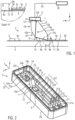
- a monitoring device 1 is used at a semiconductor device 2 ( Figure 1 ).
- the semiconductor device 2 includes a semiconductor component 3 which is typically placed on a substrate 4, and may have further electronic elements 5.
- the semi-conductor component 3 may be formed of or in the substrate 4 or be grown thereon.
- a vertical direction z is defined to extend normal from a top face or top surface 4a of the substrate 4.
- directions x, y perpendicular to each other and to the vertical direction z are defined within the top surface 4a of the substrate 4 to complete a cartesian coordinate system xyz.
- the directions x, y are horizontal directions.
- the direction x may be defined to face away from one side surface 3b of the semiconductor component 3 where a light pipe insert 7 is placed (which is described below), and the direction y is along that side surface 3b.
- both directions x, y may be defined to face away from either of these two side surfaces 3b.
- This definition of horizontal directions x,y and vertical direction z is a local definition with respect to the semiconductor device 2, which is only for ease of explanation and is independent from an orientation of the semiconductor device 2 in a global space or environment.
- the semiconductor component 3 has a top surface 3a facing in the vertical direction z, and a side surface 3b or several side surfaces 3b exposed from the top surface 4a of the substrate 4 to be accessible from a lateral side.
- the semiconductor component 3 is of a kind which exhibits an electroluminescence or photoluminescence effect such that it emits photons when biased (in case of a Diode) or reverse-biased (in case of a MOSFET). Typically such effect shows at a junction and in a region surrounding that junction which is addressed as a light emitting layer 3c.
- the light emitting layer 3c is exposed at each side surface 3b of the semiconductor element 3 to form a light emitting surface 6 of the semiconductor component 3 (detail "A" in Figure 1 ).
- the light emitting surface 6 is a light emitting portion of the side surface 3b where the light emitting layer 3c is exposed.
- thickness of a top layer covering the light emitting layer 3c of the semiconductor component 3 is shown exaggerated in the drawing.
- the thickness of the light emitting layer 3c might vary substantially within the semiconductor component 3.
- the top layer may e.g. be a passivation layer with metallised contacts on top. Light cannot transition though these layers due to thickness.
- the electroluminescence or photoluminescence effect on biasing or reverse-biasing is known to arise in direct bandgap semiconductor components made of SiC (silicon carbide), in particular SiC 4H or SiC 6H polytypes.
- the intensity of photon emission according to the electroluminescence or photoluminescence effect is a convolved response to temperature, current conditions and gate voltage (the latter for MOSFETs only).
- SiC is widely used in power modules such as power MOSFETs for a variety of appliances such as traction inverters for electric vehicles or switching power supplies. Vehicles may include automobiles, trucks, motorcycles, trains, cableways, marine vessels, aircrafts.
- the semiconductor component 3 is an SiC power MOSFET in an inverter of an automobile. It is desirable to know the temperature of the semiconductor component 3 for reliable function while exploiting its boundaries of operation. It is also desirable to know a current which the semiconductor component 3 endures, for the same reasons and for controlling the semiconductor component 3.
- the monitoring device 1 of the present embodiment is provided for collecting the photons or at least a defined fraction of the photons emitted by the semiconductor component 3 due to the electroluminescence or photoluminescence effect, for thereby detecting the temperature of the semiconductor component 3 or a current through the semiconductor component 3.
- the monitoring device 1 includes a light pipe insert 7 that is placed at the semiconductor component 3.
- the light pipe insert 7 includes a light pipe body 8.
- the light pipe body 8 is formed to conduct incident light by inner reflection from a light capturing end or light receiving end 11 to a light extraction end or light emitting end 13, see an exemplary light ray 15 in Figure 1 .
- the light pipe body 8 may have a reflective structure such as a curvature 16.
- the optimization of the path of the light rays 15 may refer to a minimum length and/or a minimum number of inner reflections.
- the light pipe body 8 has a foot section 9 which abuts the semiconductor device 2, in particular the top surface 4a of the substrate 4, and a shaft section 10 which extends from the substrate 4.
- the foot section 9 and the shaft section 10 may be integrally formed or connected with each other.
- the foot section 9 may include, be included, or coincide with the light receiving end 11 of the light pipe insert 7.
- the foot section 9 has a bottom face 9a which abuts the top surface 4a of the substrate 4, and a front face 9b which faces the side surface 3b of the semiconductor component 3.
- the front face 9b of the foot section 9 includes the light receiving surface 12 of the light pipe insert 7.
- a gap is shown between the front face 9b of the foot section 9 and the side surface 3b of the semiconductor component 3. Even if such gap may be present, it is preferable that the front face 9b of the foot section 9 tightly abuts the side surface 3b of the semiconductor component 3 to reduce phase interface transits of light. If a considerable gap is present, it is preferable that such gap is filled by a transparent filler or glue 60 (see Figure 6 ).
- the shaft section 10 has a front face 10a generally facing in a direction toward the semiconductor component 3 in the horizontal plane xy, in particular in negative x direction, and a back face 10b generally facing away from the semiconductor component 3 in the opposite direction to the front face 10a.
- the front face 10a of the shaft section has an erect part 10c generally extending in the vertical direction z, and a slant part 10d inclined from the vertical direction z away from the semiconductor component 3.
- the erect part 10c and the slant part 10d are flat. It will be noted that the front face 10a of the shaft section 10 is continuous with or coincides with the front face 9b of the foot section 9 to include the light receiving surface 12.
- a top end or top surface 10f of the shaft section 10 forms a light emitting surface 14 of the light pipe insert 7.
- the back face 10b includes the curvature 16 in x-z cross section for optimizing inner reflection. In x-y cross section, the back face 10b is flat in this embodiment which however is not limiting the invention.
- the back face 10b may have a curvature also in a cross-section perpendicular to the x-z plane and normal to the x-z curvature for focusing rays of light within the light pipe body.
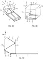
- the shaft section 10 also has two lateral faces 10e (see Figure 2 ) facing perpendicular to the facing directions of the front face 10a and the back face 10b.
- the lateral faces 10c are parallel with each other and are generally flat.
- the light pipe body 8 has a width, i.e. is a distance between the two lateral surfaces 10e, smaller than a width of the semiconductor component 3. This means that only a part of the light emitting surface 6 of the semiconductor component 3 is covered by the light receiving surface 12 of the light pipe insert 7. This in turn means that all the width of the light receiving surface 12 of the light pipe insert 7 receives light rays which are generally parallel.
- an optical sensor 17 may be coupled to receive light from a light emitting surface 14 of the light pipe body 8 ( Figure 1 ).
- the optical sensor 17 may e.g. be a photodiode which has fast response time and low cost.
- the optical sensor 17 may be coupled to a processing unit 18 via data link 19.
- the optical sensor 17 may be optionally be lensed or left un-lensed.
- a filter may optionally be provided before the sensor 17 to select for changes in specific wavelengths.
- light may optionally be brought to a preferred sensor location by free space optics, fibre optics, or a secondary light pipe system.
- the processing unit 18 may be a general purpose computer such as a laptop, desktop, phone or the like, or a special purpose control unit of an automobile, other vehicle, power plant or other appliance.
- the processing unit 18 may include a processor, data interface(s), permanent memory (ROM), working memory (RAM), flash memory, user interface(s), data reading/writing unit(s), and other elements as is generally known.
- the data link 19 may be a cable or wireless link and/or may be part of a bus structure, in particular field bus or vehicle bus such as a CAN bus, or the like.
- the optical sensor 17 is formed to output a sensor signal or sensor value in response to reception of light from the light pipe insert 7.
- the processing unit 19 is formed to receive and interpret a sensor signal from the optical sensor 17 to provide a measuring value related to the temperature and/or the current through the semiconductor component and/or its gate voltage.
- the interpretation of sensor signals may make use of dependencies between an electroluminence amount and the properties or conditions mentioned above which are determined beforehand or are known from literature. Examples of such literature are [1] J. Winkler, J. Homoth and I. Kallank, "Electroluminescence-Based Junction Temperature Measurement Approach for SiC Power MOSFETs," in IEEE Transactions on Power Electronics, vol. 35, no. 3, pp. 2990-2998, March 2020, doi: 10.1109/TPEL.2019.2929426 , and [2] S. Kalker, C. H.
- the electronics parts on the substrate 4 can be arranged within a casing 20 ( Figure 2 ).
- other parts can be arranged on the substrate 4.
- such other parts may include a power connecting unit 21 having a body part 21b and a number of connecting pins 21a-21d, conductive tracks 22a-22d of a high power wiring lines 22 leading from the power connecting unit 21 to the semiconductor component 3, the conductive tracks 22a-22d representing e.g.
- the RTD sensor 23 can be provided for measuring a temperature of the die based on a temperature-dependent resistance change, and can be used for calibrating the measurement via the light pipe insert 7 and the optical sensor 17, for testing, or as a backup. Where the measuring characteristic of the optical measurement is reliably known, the RTD sensor 23 may also be omitted.
- the RTD sensor 23 will have a delay in measurement owing to the fact that a temperature change in the semiconductor component 3 needs some time to cause a temperature change in the substrate 4 beneath the RTD sensor 23.
- the change of light emission from the semiconductor component 3 will instantaneously follow a temperature change in the semiconductor component 3, and thus can be detected instantaneously.
- the parts can be sealed by an insulating filler with only the connecting pins of the connecting units 21, 24, and the light emitting surface 14 of the light pipe insert 7 being exposed.
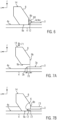
- More than one semiconductor components 3 to be individually monitored may be played on one substrate 4 (see Figs. 4A-4C where different kinds of light pipe inserts 7 are applied for purposes of illustration).
- the shape and build of the light pipe insert 7 and light pipe body 8 may be varied in numerous ways.
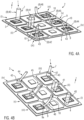
- the light pipe body 8 may be a cuboid body having rectangular faces 10a, 10b, 10e, 10f, 9a ( Figures 3A-3C ).
- An indent 30 may be formed within the bottom face 9a, having a reflective geometry to enhance guiding a ray of light 15 which enters the light receiving surface 12 into the vertical direction z, to eventually reach the light emitting surface 14.
- the indent 30 is formed only in a part of the bottom face 9a, such that abutment surfaces 31 remain for abutting the substrate.
- the indent 30 may be gently curved or polygonal, it may be curved generally in x-z cross section and may have or may not have a slight curvature also in a cross-section perpendicular to the x-z plane and normal to the x-z curvature.
- the indent 30 can be combined with any embodiment or variant shown or described herein.
- the light pipe insert 7 may be formed and placed such that the foot section 9a partially covers the top surface 3a of the semiconductor component 3 ( Figures 4A-4C ).
- the light pipe body 8 may include:
- FIG. 5A-5D Further variants of light pipe inserts 7 are shown in Figures 5A-5D , which may include:
- a method for manufacturing the semiconductor device 2 having the monitoring device 1 includes at least the following steps:
- the method may further include the step of gluing the light pipe insert 7 to the semiconductor device 2 by a glue 60 (see Figure 6 ).
- a transparent glue 60 is preferably used at least in the region of a gap between the light receiving surface 12 of the light pipe insert 7 and the light emitting surface 6 of the semiconductor component 3.
- Other parts of the light pipe insert 7, in particular in a region between the light pipe insert 7 and the substrate 4, could be fixed by an opaque glue or other methods such as e.g. friction welding.
- the opacity or transparency of the glue 60 refers to the cured state of the glue 60.
- the method may include a pressing the light pipe insert 7 to the semiconductor device 2 in a pressing direction 71 such that a bottom face 9a of the foot section 9 of the light pipe body 8 has an overlap 70 with the top surface 3a of the semiconductor component 3 ( Figure 7A ).
- the bottom face 9a may even deform under the pressure to form a step 72 which perfectly fits the contour of the semiconductor component 3 in the overlap 70, and the light receiving surface 12 of the light pipe insert 7 is formed by the forming of the step 72 to fit closely with the light emitting surface 6 of the semiconductor component 3 ( Figure 7B ).
- the step 72 may be formed beforehand in the light pipe insert 7.
- a transparent glue 60 may be applied to fill possible gapes between the light pipe insert 7 and the semiconductor component 3.
- the pressing may include a friction welding of the parts under pressure.
- the method can also include a step of applying an insulation layer 73 such as a sealing upon the semiconductor device 2 which covers the substrate 4 and semiconductor device 3 as well as other electronic elements 5, wirings 22, 24 etc. while the light pipe insert 7 as well as e.g. connectors of connecting units 21, 24 extend through the insulation layer 73 ( Figure 7B ).
- the insulation layer 73 may typically be opaque.
- the providing of the light pipe insert 7 may include a forming the light pipe body 8, in particular by at least one of injection moulding, press-forming, die-cast moulding, gravity moulding, continuous casting (and chopping into parts of proper length), thermoforming, detailing, cutting, bending and/or twisting, finishing, surface treatment, mirror-coating, gloss-coating, opaque coating, polishing, roughening, assembling with other parts such as collar 43 or crosstalk barrier 53, as far as not formed together with the light pipe body 8.
- a forming the light pipe body 8 in particular by at least one of injection moulding, press-forming, die-cast moulding, gravity moulding, continuous casting (and chopping into parts of proper length), thermoforming, detailing, cutting, bending and/or twisting, finishing, surface treatment, mirror-coating, gloss-coating, opaque coating, polishing, roughening, assembling with other parts such as collar 43 or crosstalk barrier 53, as far as not formed together with the light pipe body 8.
- the light pipe body 8 is formed as a solid monolithic body made of a transparent material such as a transparent polymer or a typical glass, including NBK7, Quartz, Sapphire, PE, PET, PMMA, Acrylic, PC, PETG, PVC, LSR, COCs, SAN, GPPS, ABS, MABS.
- Reflecting surfaces of the light pipe body 8 may be coated with a reflective or mirror coating.
- Other surfaces may be coated with a glossy coating or an opaque coating.
- a glossy coating can be useful e.g. for enhancing boundary transit at light receiving/emitting surfaces, and an opaque coating can be useful e.g. for shielding side emission or incidence from/into the light pipe body 8.
- the method preferably includes coupling a light sensor to the light emitting end 13 of the light pipe insert 7, and connecting the optical sensor 17 with processing unit 18.
- Any light pipe insert 7 described and depicted in this application can be provided separately to be used in or as a monitoring device and can establish an individual embodiment of the invention, with or without further equipment such as optical sensor 17, processing unit 18, link 19, or the like.
- multiple semiconductor components 3 may be provided, each being monitored by an individual light pipe insert 7.
- Each light pipe insert 7 may be coupled to an individual optical sensor 17.
- light emitted from multiple light pipe inserts 7 may be coupled to one optical sensor in parallel or serially or in interlaced or scanned fashion.
- the monitoring device 1 using the light pipe inserts 7 according to the invention described herein exhibits the following advantages:
- the monitoring device 1 allows execution of a method for monitoring a semiconductor component for an automobile appliance under high current and/or by a monitoring device, said semiconductor element emitting photons when biased, by way of electroluminescence or photoluminescence, in an amount depending on temperature and/or current through the semiconductor component and/or its gate voltage, in particular including silicon carbide, said monitoring device being preferably formed according to any of the preceding claims, the method including:
Landscapes
- Physics & Mathematics (AREA)
- General Physics & Mathematics (AREA)
- Health & Medical Sciences (AREA)
- Engineering & Computer Science (AREA)
- General Health & Medical Sciences (AREA)
- Nuclear Medicine, Radiotherapy & Molecular Imaging (AREA)
- Analytical Chemistry (AREA)
- Biochemistry (AREA)
- Life Sciences & Earth Sciences (AREA)
- Immunology (AREA)
- Pathology (AREA)
- Chemical & Material Sciences (AREA)
- Computer Vision & Pattern Recognition (AREA)
- Electromagnetism (AREA)
- Toxicology (AREA)
- General Engineering & Computer Science (AREA)
- Photo Coupler, Interrupter, Optical-To-Optical Conversion Devices (AREA)
- Testing Or Measuring Of Semiconductors Or The Like (AREA)
Abstract
Description
- The invention relates to a monitoring device for a semiconductor component, a semiconductor device and a method for manufacturing the same.
- Semiconductor and compound semiconductors components for a variety of appliances, such as power train inverters, produce heat, and receive heat from other sources, which may raise the temperature of the semiconductor component. The temperature of the semiconductors forms one of the limits for wider system operation as excess temperature leads to catastrophic failure, but approaching the limit is often desirable from a performance perspective. Further, individual semiconductors are often used in groups and may not see identical current loading nor heating. There is therefore a demand for measuring or monitoring the temperature of critical semiconductor components, both individually and in groups. Operation of a semiconductor component may also be limited by a current running therethrough, so that knowledge of the current is also highly useful.
- Known methods for measuring or monitoring the temperature of a semiconductor component, e.g. of a power module, suffer from the need to isolate temperature sensing elements from the high voltage present. I.e., the placement of temperature sensors in the prior art is associated with gaps in thermal paths, leading to a low responsiveness to fast temperature rises. A low responsiveness to these fast transient temperature changes significantly limits the accuracy and utility of the measurement. The more accurately temperature is measured, the more accurately power draw of a specific device can be interpreted. Once a specific device temperature is known, conclusions can be drawn about device health and performance limits, moreover this can be specific to the exact build.
- It is known e.g. from
JP2018107166A -
CN112485241A andCN112180227A disclose that detecting light emission of a SiC power device can be used for contact-less synchronous online detection of junction temperature and current of the silicon carbide power device working in high-temperature, high-voltage and high-current application occasions, with high precision and real-time performance. The measurement is done by a photoelectric detection circuit which receives the light from a light guide which is made of low-loss silica fibre. Fibre optics are however delicate to handle and connect, designed for high-intensity light sources, and sensitive to vibrations which usually occur in automobile appliances and other fields. In particular, a slight deviation in an angle or position under which a light guide is situated with respect to a light source can drastically change the amount of light coupled into the light guide. Similar problems can occur at the light emitting side of the light guide where the light is coupled out to be received by an optical sensor. Under strong vibrations, such deviations can occur which might be small but still have a strong impact on the light received, transported, and emitted by a light guide, thereby affecting reliably of light measurement, and conclusion drawn from such measurement. Moreover, a light receiving surface of a light guide is usually small, as it is adapted to receive strong light signals such as from a laser or LED. The photoluminescence or electroluminescence effects of an SiC die however are a side effect which is not very intense, as compared with common fibre optic laser light sources which are designed for high output. Also, the light emission of an SiC component is not concentrated but is distributed over a broad region all along a side surface of the component. For effectively collecting light of a relatively weak and dispersed source into a light guide, highly complex coupling setup would have to be developed and used. The mounting of such coupling setup with the die and with the light guide must be made with high precision and typically comprises either a lens stack or a lensed fibre. Therefore, temperature measurement or current measurement based on a light output of an SiC component under strong vibrations such as in automotive appliances is neither reliable nor cost effective with the solutions available in the art. - A technical problem of the invention is to create a monitoring device and method which enables accurate, responsive and reliable measurement of temperature or current of a semiconductor component under high current load even under rough mechanical conditions by utilizing electroluminescence or photoluminescence effects of the semiconductor element while enabling easy manufacture and providing resilient structure, a semiconductor device including a semiconductor component having such monitoring device, and a method for manufacturing the same.
- The technical problem is solved by the features of the independent claims. Further developments and advantageous embodiments are set forth in the subclaims.
- An aspect of the invention is a monitoring device for a semiconductor component for an automobile appliance under high current and/or voltage, said semiconductor component emitting photons at a light emitting surface when biased or reverse-biased, by way of electroluminescence or photoluminescence, in an amount depending on a temperature of, and/or a current through the semi-conductor component and/or its gate voltage, wherein the semi-conductor component comprises particularly silicon carbide, the monitoring device including a light pipe insert having a light receiving end or light capturing end and a light emitting end or light extraction end, the light pipe insert being formed and placed to receive photoluminescence light or electroluminescence light from the semiconductor component through a light receiving surface at the light receiving end and to conduct the received light to the light emitting end for detecting the temperature of the semi-conductor component and/or a current through the semiconductor component and/or a gate voltage of the semiconductor component through an optical sensor coupled to the light emitting end of the light pipe insert.
- A light pipe is a rigid body which is easy and inexpensive to manufacture, to handle and to mount. It can have a relatively large light receiving surface which is able to collect light over an elongated area like the side surface of an SiC die. The position and orientation of the light pipe with respect to the die or a sensor is not that critical like with a fibre-type light guide which typically has a narrow depth-of-field, at least within the boundaries of deviations expectable by vibration and assembly-tolerances in an automobile appliance. A complex and fragile coupling setup is not needed at the light receiving end or the light emitting end of a light pipe. By use of a light pipe insert according to the invention therefore enables accurate, responsive and reliable measurement of temperature and/or current of a semiconductor component and/or its gate voltage under high current load even under rough mechanical conditions by utilizing electroluminescence or photoluminescence effects of the semiconductor element while enabling easy manufacture and providing resilient structure, allowing for an indirect measurement by sensing the photon output linked with the respective condition. It will be noted that the semiconductor component may be a compound semiconductor component.
- The semiconductor component may have a flat top surface and one or more side surfaces which surround the top surface and extend from a top surface or top face of a substrate where the semiconductor component is provided. The semiconductor component may have a light emitting surface formed in at least one side surface of the semiconductor component, and the light receiving surface of the light pipe insert faces at least part of the light emitting surface of the semiconductor component. That part of the light emitting surface may be at a straight part or a curved part of one side surface or a corner part of two side surfaces of the semiconductor component.
- In embodiments, the light pipe insert may have a back face opposite to the light receiving surface, the back face being formed, preferably curved, to reflect light incident from the light receiving surface to a light emitting surface or light extraction surface provided at the light emitting end of the light pipe insert.
- In embodiments, the light pipe insert may have a bottom face extending from the light receiving surface, the bottom face including an abutment surface and at least one indent being formed, preferably curved, to reflect light incident from the light receiving surface in a generally vertical direction to a light emitting surface provided at the light emitting end of the light pipe insert. The abutment surface may be formed to abut a surface of a substrate where the semiconductor component is provided.
- In embodiments, light reflecting surfaces of the light pipe insert may be formed, preferably curved, in a direction across a path of light incident from the light receiving surface to focus the light to a point or a confined region within a light emitting surface provided at the light emitting end of the light pipe insert.
- In embodiments, the light pipe insert may have a reflective or mirror-coating or reflection-enhancing surface treatment to improve internal reflection. This can be limited to particular reflective surfaces or surface parts, and can help transmitting the light with minimum loss due to side emission or absorption. Where the light pipe body is cylindrical, the reflective treatment may be all over the side surfaces.
- Also, the light pipe insert may have an opaque coating or surface treatment to prevent transmission of light at surfaces other than the light receiving surface or a light emitting surface provided at the light emitting end of the light pipe insert. This can be limited to particular surfaces or surface parts, and can help avoiding side emission of light as well as incidence of light from outside. Such opacitizing treatment may be applied in addition to a reflective treatment.
- Moreover, the light pipe insert may have a glossy coating or surface treatment to improve transmission of light at the light receiving surface or the light emitting surface of the light pipe insert.
- Moreover, the light pipe insert may have a reflective coating or surface treatment to increase internal reflection, and improve the transmission of light along the light pipe's transmission path.
- Furthermore, the light pipe insert may have an optical element such as a spherical or aspherical or Fresnel lens surface or lens stack at the light emitting end which may help capturing, focusing, and directing the light at the light emitting end.
- In embodiments, the light pipe insert may comprise a light pipe body having a foot section at the light receiving end and a shaft section extending from the foot section to the light emitting end, wherein the foot section preferably has a wider cross-sectional area than the shaft section. The foot section may be formed to rest on a top surface or top face of a substrate where the semiconductor component is provided. With a wider cross-sectional are, mounting stability may be improved. The foot section may for example be formed like a collar. The shaft section may have any useful shape, and may have a swept rectangular profile, polygon, circular, elliptical profile, to form a straight, angled or curved (in one or more dimensions) piece. A swept profile in the sense of this application is a profile which has a similar cross-section at any place cut, but may follow an arbitrary path.
- Here, the foot section may partly overlap a top surface of the semiconductor component. In other words, the foot section may rest on both top surfaces of the substrate and the semi-conductor component which improves rigidity and reliability of mount, and ensures constant positioning of the light pipe insert with respect to the semiconductor component so that the direction of incident light can be held constant. For providing the overlap, the foot section may form a step, and the vertical part of the step may include the light receiving surface of the light pipe insert.
- A gap between the light receiving surface of the light pipe insert and the light emitting surface of the semiconductor component may be filled with a transparent or semi-transparent medium such as glue or silicone.
- If the foot section of the light pipe insert is thermally deformable, the foot section may be adapted to the shape of the semiconductor component during mounting such that the aforementioned step and the light receiving surface are exactly adapted to the semiconductor component. Here, a temperature range of thermal deformability is preferably well beyond a temperature which is expected to occur during operation of the semiconductor component, and well beneath a temperature the semiconductor component can passively endure without damage.
- Preferably, the light pipe body is a solid monolithic body made of a transparent material such as a transparent polymer or a typical glass. These materials are naturally insulating, retaining the isolating function of an encapsulant of the semiconductor component, while achieving light conducting functions.
- The monitoring device may further comprise an optical sensor formed and arranged for receiving light from a light emitting end of the light pipe insert, and provide sensor signals related to the received light from the light pipe insert. The optical sensor may be placed directly at a light emitting end of the light pipe insert, or at a remote location with the light from the light pipe insert being led to the sensor by other means.
- The monitoring device may also further comprise a control unit formed for receiving and interpreting the sensor signals from the optical sensor to provide a sensor value related to the temperature of or a current through the semiconductor component the light pipe is placed at.
- A further aspect of the invention is a semiconductor device for an automobile appliance, the semiconductor device comprising:
- a semiconductor component to be operated under high current and/or high voltage and emitting photons at a light emitting surface when biased or reverse-biased, by way of electroluminescence or photoluminescence, in an amount depending on temperature of and/or current through the semiconductor component and/or its gate voltage, the semiconductor component particularly comprising silicon carbide; and
- a monitoring device formed and arranged for detecting the temperature of the semiconductor component or a current through the semiconductor component based on photoluminescence light or electroluminescence light captured from the semiconductor component, wherein the monitoring device includes a light pipe insert having a light receiving end including a light receiving surface and a light emitting end, and placed at the semiconductor component such that the light receiving surface faces at least part of the light emitting surface of the semiconductor component, the light pipe insert being formed to conduct light received at the light receiving end to the light emitting end, the light emitting end being formed to be coupled to an optical sensor for detecting the temperature of the semiconductor component and/or a current through the semiconductor component and/or a gate voltage of the semi-conductor component, wherein the monitoring device is particularly formed according to the previous aspect including any of its embodiments,
- Here, the optical sensor senses a photon output linked with the temperature and/or current and/or gate voltage, and detection of the temperature and/or current and/or gate voltage makes use of that linkage.
- A further aspect of the invention is a method for manufacturing the afore-described semi-conductor device, the method comprising:
- placing the light pipe insert on a surface region adjacent to the semiconductor component such that the light receiving surface of the light pipe insert faces at least part of a light emitting surface of the semiconductor component;
- fixing the light pipe insert; and
- covering the semiconductor component by an insulation layer such that the light pipe extends through and out of the insulation layer,
wherein the fixing preferably includes connecting the light receiving end of the light pipe insert with the surface region adjacent to the semiconductor component, wherein the connecting includes at least one of: - pressing,
- glueing, preferably by an optical glue,
- thermally deforming
a foot section including the light receiving end of the light pipe insert. - The invention will now be further described in view of exemplary embodiment, referring to the accompanying drawings. In the drawings,
- Fig. 1
- is a schematical side view of a semiconductor device having a monitoring device according to an embodiment of the invention, including an enlarged detail "A";
- Fig. 2
- is a perspective view of a semiconductor device having a monitoring device according to another embodiment of the invention;
- Fig. 3A-3B
- are a perspective view of a monitoring device according to another embodiment of the invention, a perspective view of a light pipe in the monitoring device, and a side view of the monitoring device with an exemplary optical path within the light pipe;
- Fig. 4A-4C
- are two perspective views and a top view of monitoring devices including six particular variations of light pipes according to further embodiments of the invention, according to cases i-vi;
- Fig. 5A-5D
- are schematical views of further particular variations of light pipes for monitoring devices according to further embodiments of the invention;
- Fig. 6
- is a side view of a monitoring device according to a further embodiment of the invention;
- Fig. 7A, 7B
- are side views of manufacturing stages of a monitoring device according to a further embodiment of the invention;
- It will be noted that the drawings are schematic by nature and are made to illustrate preferred examples for embodying the invention, so that its concept can be understood.
- A
monitoring device 1 according to an exemplary embodiment is used at a semiconductor device 2 (Figure 1 ). - The
semiconductor device 2 includes asemiconductor component 3 which is typically placed on asubstrate 4, and may have further electronic elements 5. In some instances, thesemi-conductor component 3 may be formed of or in thesubstrate 4 or be grown thereon. For the purposes of this description, a vertical direction z is defined to extend normal from a top face ortop surface 4a of thesubstrate 4. Likewise, directions x, y perpendicular to each other and to the vertical direction z are defined within thetop surface 4a of thesubstrate 4 to complete a cartesian coordinate system xyz. The directions x, y are horizontal directions. Here, the direction x may be defined to face away from oneside surface 3b of thesemiconductor component 3 where alight pipe insert 7 is placed (which is described below), and the direction y is along thatside surface 3b. Where thelight pipe insert 7 is placed at a corner of twoside surfaces 3b of the semiconductor component 3 (see e.g. cases i, iii, iv inFigures 4A-4C ), both directions x, y may be defined to face away from either of these twoside surfaces 3b. This definition of horizontal directions x,y and vertical direction z is a local definition with respect to thesemiconductor device 2, which is only for ease of explanation and is independent from an orientation of thesemiconductor device 2 in a global space or environment. - The
semiconductor component 3 has atop surface 3a facing in the vertical direction z, and aside surface 3b orseveral side surfaces 3b exposed from thetop surface 4a of thesubstrate 4 to be accessible from a lateral side. Thesemiconductor component 3 is of a kind which exhibits an electroluminescence or photoluminescence effect such that it emits photons when biased (in case of a Diode) or reverse-biased (in case of a MOSFET). Typically such effect shows at a junction and in a region surrounding that junction which is addressed as alight emitting layer 3c. Thelight emitting layer 3c is exposed at eachside surface 3b of thesemiconductor element 3 to form alight emitting surface 6 of the semiconductor component 3 (detail "A" inFigure 1 ). In other words, thelight emitting surface 6 is a light emitting portion of theside surface 3b where thelight emitting layer 3c is exposed. It will be noted that thickness of a top layer covering thelight emitting layer 3c of thesemiconductor component 3 is shown exaggerated in the drawing. The thickness of thelight emitting layer 3c might vary substantially within thesemiconductor component 3. The top layer may e.g. be a passivation layer with metallised contacts on top. Light cannot transition though these layers due to thickness. The electroluminescence or photoluminescence effect on biasing or reverse-biasing is known to arise in direct bandgap semiconductor components made of SiC (silicon carbide), in particular SiC 4H or SiC 6H polytypes. The intensity of photon emission according to the electroluminescence or photoluminescence effect is a convolved response to temperature, current conditions and gate voltage (the latter for MOSFETs only). SiC is widely used in power modules such as power MOSFETs for a variety of appliances such as traction inverters for electric vehicles or switching power supplies. Vehicles may include automobiles, trucks, motorcycles, trains, cableways, marine vessels, aircrafts. In the present embodiment, thesemiconductor component 3 is an SiC power MOSFET in an inverter of an automobile. It is desirable to know the temperature of thesemiconductor component 3 for reliable function while exploiting its boundaries of operation. It is also desirable to know a current which thesemiconductor component 3 endures, for the same reasons and for controlling thesemiconductor component 3. - The
monitoring device 1 of the present embodiment is provided for collecting the photons or at least a defined fraction of the photons emitted by thesemiconductor component 3 due to the electroluminescence or photoluminescence effect, for thereby detecting the temperature of thesemiconductor component 3 or a current through thesemiconductor component 3. For this purpose, themonitoring device 1 includes alight pipe insert 7 that is placed at thesemiconductor component 3. Thelight pipe insert 7 includes alight pipe body 8. Thelight pipe body 8 is formed to conduct incident light by inner reflection from a light capturing end orlight receiving end 11 to a light extraction end orlight emitting end 13, see anexemplary light ray 15 inFigure 1 . For optimizing a path of the light rays 15, thelight pipe body 8 may have a reflective structure such as acurvature 16. The optimization of the path of the light rays 15 may refer to a minimum length and/or a minimum number of inner reflections. - The
light pipe body 8 has afoot section 9 which abuts thesemiconductor device 2, in particular thetop surface 4a of thesubstrate 4, and ashaft section 10 which extends from thesubstrate 4. Thefoot section 9 and theshaft section 10 may be integrally formed or connected with each other. Thefoot section 9 may include, be included, or coincide with thelight receiving end 11 of thelight pipe insert 7. - In the present embodiment, the
foot section 9 has abottom face 9a which abuts thetop surface 4a of thesubstrate 4, and afront face 9b which faces theside surface 3b of thesemiconductor component 3. Thereby, thefront face 9b of thefoot section 9 includes thelight receiving surface 12 of thelight pipe insert 7. It will be noted that in the enlarged detail "A" ofFigure 1 , a gap is shown between thefront face 9b of thefoot section 9 and theside surface 3b of thesemiconductor component 3. Even if such gap may be present, it is preferable that thefront face 9b of thefoot section 9 tightly abuts theside surface 3b of thesemiconductor component 3 to reduce phase interface transits of light. If a considerable gap is present, it is preferable that such gap is filled by a transparent filler or glue 60 (seeFigure 6 ). - In the present embodiment, the
shaft section 10 has afront face 10a generally facing in a direction toward thesemiconductor component 3 in the horizontal plane xy, in particular in negative x direction, and aback face 10b generally facing away from thesemiconductor component 3 in the opposite direction to thefront face 10a. Thefront face 10a of the shaft section has anerect part 10c generally extending in the vertical direction z, and aslant part 10d inclined from the vertical direction z away from thesemiconductor component 3. Theerect part 10c and theslant part 10d are flat. It will be noted that thefront face 10a of theshaft section 10 is continuous with or coincides with thefront face 9b of thefoot section 9 to include thelight receiving surface 12. At thelight emitting end 13, a top end ortop surface 10f of theshaft section 10 forms alight emitting surface 14 of thelight pipe insert 7. Theback face 10b includes thecurvature 16 in x-z cross section for optimizing inner reflection. In x-y cross section, theback face 10b is flat in this embodiment which however is not limiting the invention. Theback face 10b may have a curvature also in a cross-section perpendicular to the x-z plane and normal to the x-z curvature for focusing rays of light within the light pipe body. - The
shaft section 10 also has twolateral faces 10e (seeFigure 2 ) facing perpendicular to the facing directions of thefront face 10a and theback face 10b. In other words, the lateral faces 10c are parallel with each other and are generally flat. In the present embodiment, thelight pipe body 8 has a width, i.e. is a distance between the twolateral surfaces 10e, smaller than a width of thesemiconductor component 3. This means that only a part of thelight emitting surface 6 of thesemiconductor component 3 is covered by thelight receiving surface 12 of thelight pipe insert 7. This in turn means that all the width of thelight receiving surface 12 of thelight pipe insert 7 receives light rays which are generally parallel. - At the
light emitting end 13 of thelight pipe insert 7, anoptical sensor 17 may be coupled to receive light from alight emitting surface 14 of the light pipe body 8 (Figure 1 ). Theoptical sensor 17 may e.g. be a photodiode which has fast response time and low cost. Theoptical sensor 17 may be coupled to aprocessing unit 18 viadata link 19. Theoptical sensor 17 may be optionally be lensed or left un-lensed. A filter may optionally be provided before thesensor 17 to select for changes in specific wavelengths. Instead of directly coupling thesensor 17 with thelight emitting end 13 of thelight pipe insert 7, light may optionally be brought to a preferred sensor location by free space optics, fibre optics, or a secondary light pipe system. Theprocessing unit 18 may be a general purpose computer such as a laptop, desktop, phone or the like, or a special purpose control unit of an automobile, other vehicle, power plant or other appliance. Theprocessing unit 18 may include a processor, data interface(s), permanent memory (ROM), working memory (RAM), flash memory, user interface(s), data reading/writing unit(s), and other elements as is generally known. The data link 19 may be a cable or wireless link and/or may be part of a bus structure, in particular field bus or vehicle bus such as a CAN bus, or the like. Theoptical sensor 17 is formed to output a sensor signal or sensor value in response to reception of light from thelight pipe insert 7. Theprocessing unit 19 is formed to receive and interpret a sensor signal from theoptical sensor 17 to provide a measuring value related to the temperature and/or the current through the semiconductor component and/or its gate voltage. The interpretation of sensor signals may make use of dependencies between an electroluminence amount and the properties or conditions mentioned above which are determined beforehand or are known from literature. Examples of such literature are [1] J. Winkler, J. Homoth and I. Kallfass, "Electroluminescence-Based Junction Temperature Measurement Approach for SiC Power MOSFETs," in IEEE Transactions on Power Electronics, vol. 35, no. 3, pp. 2990-2998, March 2020, doi: 10.1109/TPEL.2019.2929426, and [2] S. Kalker, C. H. van der Broeck, L. A. Ruppert and R. W. De Doncker, "Next Generation Monitoring of SiC mosfets Via Spectral Electroluminescence Sensing," in IEEE Transactions on Industry Applications, vol. 57, no. 3, pp. 2746-2757, May-June 2021, doi: 10.1109/TIA.2021.3062773, disclosures of which in terms of the said dependencies are included by reference. - In the
semiconductor device 2, the electronics parts on thesubstrate 4 can be arranged within a casing 20 (Figure 2 ). Besides thesemiconductor component 3, other parts can be arranged on thesubstrate 4. In an exemplary embodiment which is neither limiting nor exhaustive, such other parts may include apower connecting unit 21 having abody part 21b and a number of connectingpins 21a-21d,conductive tracks 22a-22d of a highpower wiring lines 22 leading from thepower connecting unit 21 to thesemiconductor component 3, theconductive tracks 22a-22d representing e.g. a source track, a drain track, a gate track and a ground track, anRTD sensor 23, asensor connecting unit 24 havingconnection pins conductive tracks sensor wiring lines 25, an so on. TheRTD sensor 23 can be provided for measuring a temperature of the die based on a temperature-dependent resistance change, and can be used for calibrating the measurement via thelight pipe insert 7 and theoptical sensor 17, for testing, or as a backup. Where the measuring characteristic of the optical measurement is reliably known, theRTD sensor 23 may also be omitted. It will be noted that theRTD sensor 23 will have a delay in measurement owing to the fact that a temperature change in thesemiconductor component 3 needs some time to cause a temperature change in thesubstrate 4 beneath theRTD sensor 23. In contrast, the change of light emission from thesemiconductor component 3 will instantaneously follow a temperature change in thesemiconductor component 3, and thus can be detected instantaneously. The parts can be sealed by an insulating filler with only the connecting pins of the connectingunits light emitting surface 14 of thelight pipe insert 7 being exposed. - More than one
semiconductor components 3 to be individually monitored may be played on one substrate 4 (seeFigs. 4A-4C where different kinds of light pipe inserts 7 are applied for purposes of illustration). - The shape and build of the
light pipe insert 7 andlight pipe body 8 may be varied in numerous ways. - For example, the
light pipe body 8 may be a cuboid body havingrectangular faces Figures 3A-3C ). Anindent 30 may be formed within thebottom face 9a, having a reflective geometry to enhance guiding a ray of light 15 which enters thelight receiving surface 12 into the vertical direction z, to eventually reach thelight emitting surface 14. Theindent 30 is formed only in a part of thebottom face 9a, such that abutment surfaces 31 remain for abutting the substrate. Theindent 30 may be gently curved or polygonal, it may be curved generally in x-z cross section and may have or may not have a slight curvature also in a cross-section perpendicular to the x-z plane and normal to the x-z curvature. Theindent 30 can be combined with any embodiment or variant shown or described herein. - The
light pipe insert 7 may be formed and placed such that thefoot section 9a partially covers thetop surface 3a of the semiconductor component 3 (Figures 4A-4C ). - In variants (i) to (vi) of light pipe inserts 7 shown in
Figures 4A-4C , thelight pipe body 8 may include: - (i) a flush
cylindrical body 40 which extends vertically from thesubstrate 4, - (ii) a flush
cuboid body 41 which extends vertically from thesubstrate 4, - (iii) a stepped
cylindrical body 42 which extends vertically from thesubstrate 4, having aslender shaft section 10 andwider foot section 9 formed like acollar 43, - (iv) a stepped tilted
cylindrical body 44 like in variant (iii) just that theslender shaft section 10 is inclined with respect to the vertical direction z, - (v) a stepped
parallelepiped body 45, having a parallepiped-like shaft section 10 andcuboid foot section 9 extending horizontally, - (vi) bent
cylindrical body 46 having ashaft section 10 formed as a bent slender pipe being continuous with thefoot section 9 which extends horizontally to lay upon thesubstrate 4 and partly extending over thesemiconductor component 3. - It will be noted that in each of cases (ii), (v), (vi) the
light receiving surface 6 of thelight pipe insert 7 faces a straight part of oneside surface 3b of thesemiconductor component 3, and in each of cases (i), (iii), (iv) thelight receiving surface 6 of thelight pipe insert 7 faces a corner part where twoside surfaces 3b of thesemiconductor component 3 meet. All the forms are designed for optimization in view of conduction of light from thelight receiving end 11 to thelight emitting end 13 of thelight pipe insert 7, and stability of mount of the light pipe insert 7on thesemiconductor device 2. - Further variants of light pipe inserts 7 are shown in
Figures 5A-5D , which may include: - a
light pipe body 8 having a tortuous cylindrical body 50 (Figure 5A ) where thecylindrical shaft portion 10 is bent in more than one direction after vertically emerging from thefoot portion 9, - a
light emitting end 13 having thelight emitting surface 14 with a spherical lens structure 51 (Figure 5B ) for focusing emitted light preferentially, - a
light emitting end 13 having thelight emitting surface 14 with a Fresnel-lens structure 52 (Figure 5C ) for directing emitted light, - a
crosstalk barrier 53 in the form of an opaque pipe part sheathing thelight emitting end 13 and extending beyond thetop surface 10f of theshaft section 10 to form a shrouded exit (Figure 5D ) which allows the use of several light pipe inserts simultaneously. - Many other variants and options are possible, such as the following:
- Any reflecting surface may be straight, curved in one dimension to focus the light upwards, i.e., in the direction of the
light emitting end 13, or curved in two dimensions to focus to a particular point or region in thelight emitting surface 14. Where such curvature appears convex from an outside view which in most cases will be preferable, it will have the effect of a concave curvature to internal reflection, and vice versa. - Any reflecting surface may have a reflective coating or other surface treatment. Such coating or treatment may be designed to effect all or some wavelengths.
- The light pipe body may have indents or voids to encourage or channel internal reflection.
- The
light emitting surface 14 of thelight pipe insert 7 may have a shape, coating or other surface treatment to filter or let pass desired wavelengths. - The
light emitting end 13 may have alight emitting surface 14 with an aspherical lens structure or comprise a lens stack for focusing emitted light preferentially. - The
light pipe insert 7 may have a single refractive index at all points, or may be varied to achieve focusing using Gradient Index Imaging Optics. - The
light pipe insert 7 may be optically coherent to preserve the image of the side of thesemiconductor component 3, allowing measurement of specific points on the die. - The
light pipe insert 7 may comprise a final surface incorporating a diffractive optical element. Here, a grating may be provided which is made to separate the light spatially by wavelength, allowing a sensor to only receive light from a narrow band of interest. - It will be noted that any variants or options may be mixed with each other and any embodiment shown or described herein, subject to feasibility and consistency.
- A method for manufacturing the
semiconductor device 2 having themonitoring device 1 includes at least the following steps: - providing the
light pipe insert 7; and - arranging the
light pipe insert 7 at thesemiconductor component 3 such that alight receiving surface 12 of thelight pipe insert 7 faces alight emitting surface 6 of thesemiconductor component 3. - In a particular embodiment, the method may further include the step of gluing the
light pipe insert 7 to thesemiconductor device 2 by a glue 60 (seeFigure 6 ). Here, atransparent glue 60 is preferably used at least in the region of a gap between the light receivingsurface 12 of thelight pipe insert 7 and thelight emitting surface 6 of thesemiconductor component 3. Other parts of thelight pipe insert 7, in particular in a region between thelight pipe insert 7 and thesubstrate 4, could be fixed by an opaque glue or other methods such as e.g. friction welding. It will be understood that the opacity or transparency of theglue 60 refers to the cured state of theglue 60. - In another embodiment, the method may include a pressing the
light pipe insert 7 to thesemiconductor device 2 in a pressing direction 71 such that abottom face 9a of thefoot section 9 of thelight pipe body 8 has anoverlap 70 with thetop surface 3a of the semiconductor component 3 (Figure 7A ). Here, thebottom face 9a may even deform under the pressure to form astep 72 which perfectly fits the contour of thesemiconductor component 3 in theoverlap 70, and thelight receiving surface 12 of thelight pipe insert 7 is formed by the forming of thestep 72 to fit closely with thelight emitting surface 6 of the semiconductor component 3 (Figure 7B ). - The embodiments of the method can also be combined. For example, the
step 72 may be formed beforehand in thelight pipe insert 7. Here, atransparent glue 60 may be applied to fill possible gapes between thelight pipe insert 7 and thesemiconductor component 3. On the other hand, the pressing may include a friction welding of the parts under pressure. - The method can also include a step of applying an
insulation layer 73 such as a sealing upon thesemiconductor device 2 which covers thesubstrate 4 andsemiconductor device 3 as well as other electronic elements 5, wirings 22, 24 etc. while thelight pipe insert 7 as well as e.g. connectors of connectingunits Figure 7B ). Theinsulation layer 73 may typically be opaque. - The providing of the
light pipe insert 7 may include a forming thelight pipe body 8, in particular by at least one of injection moulding, press-forming, die-cast moulding, gravity moulding, continuous casting (and chopping into parts of proper length), thermoforming, detailing, cutting, bending and/or twisting, finishing, surface treatment, mirror-coating, gloss-coating, opaque coating, polishing, roughening, assembling with other parts such ascollar 43 orcrosstalk barrier 53, as far as not formed together with thelight pipe body 8. - The
light pipe body 8 is formed as a solid monolithic body made of a transparent material such as a transparent polymer or a typical glass, including NBK7, Quartz, Sapphire, PE, PET, PMMA, Acrylic, PC, PETG, PVC, LSR, COCs, SAN, GPPS, ABS, MABS. Reflecting surfaces of thelight pipe body 8 may be coated with a reflective or mirror coating. Other surfaces may be coated with a glossy coating or an opaque coating. A glossy coating can be useful e.g. for enhancing boundary transit at light receiving/emitting surfaces, and an opaque coating can be useful e.g. for shielding side emission or incidence from/into thelight pipe body 8. - The method preferably includes coupling a light sensor to the
light emitting end 13 of thelight pipe insert 7, and connecting theoptical sensor 17 withprocessing unit 18. - Any
light pipe insert 7 described and depicted in this application can be provided separately to be used in or as a monitoring device and can establish an individual embodiment of the invention, with or without further equipment such asoptical sensor 17, processingunit 18, link 19, or the like. - As said above, in a semiconductor device,
multiple semiconductor components 3 may be provided, each being monitored by an individuallight pipe insert 7. Eachlight pipe insert 7 may be coupled to an individualoptical sensor 17. Alternatively, light emitted from multiple light pipe inserts 7 may be coupled to one optical sensor in parallel or serially or in interlaced or scanned fashion. - The
monitoring device 1 using the light pipe inserts 7 according to the invention described herein exhibits the following advantages: - The cost are low, so the invention is suited for use in volume applications. The light pipe inserts 7 are substantially cheaper to implement than fibre optic methods. A single insert is producible e.g. by injection moulding from an inexpensive polymer, or a typical glass. It avoids the use of expensive fibre-optics, and removes the need for board-level signal pins thus reducing component count.
- The
light pipe insert 7 is a mechanically robust component in comparison with fibre optics. It is naturally insulating, retaining the isolating function of the encapsulant, while achieving the light transporting function. - The invention is suitable for use adjacent to high voltage components and/or high temperature components.
- The
light pipe insert 7 may be placed closer to the source of heat (ie., the semiconductor component 3) than temperature sensors can be at present, due to voltage safety and practical circuit design e.g. track and gap. - The
light pipe insert 7 withoptical sensor 17 will provide a temperature reading several orders of magnitude faster than a board-mounted sensor likeRTD sensor 23. Thereby, fast sensing regimes are enabled, with lower cost board level sensors. - The invention provides a direct temperature measurement while other sensors estimate the temperature of the die as the distance guarantees a difference between the die and a traditional sensor. The invention using the
light pipe insert 7 overcomes this, and provides rapid feedback. The temperature signal is decoupled from the noise generating substrate. - The invention may be used to understand the current in a specific die [chip], given die vary, this is a big advantage as it is not possible with conventional methods.
- The
monitoring device 1 allows execution of a method for monitoring a semiconductor component for an automobile appliance under high current and/or by a monitoring device, said semiconductor element emitting photons when biased, by way of electroluminescence or photoluminescence, in an amount depending on temperature and/or current through the semiconductor component and/or its gate voltage, in particular including silicon carbide, said monitoring device being preferably formed according to any of the preceding claims, the method including: - using a monitoring device, preferably formed according to any of the preceding claims, having a light pipe placed at the semiconductor component such that a light receiving surface of the light pipe can receive electroluminescence or photoluminescence light emitted from the semiconductor component;
- receiving light from a light emitting end of a light pipe which is placed at the semi-conductor component such that a light receiving surface of the light pipe can receive light emitted from the semiconductor component;
- providing sensor signals related to the received light from the light pipe; and
- interpreting the sensor signals to provide a measuring value related to the temperature of and/or current through the semiconductor component and/or its gate voltage.
- This list is integral part of the description.
| 1 | | 19 | | |
| 2 | | 20 | | |
| 3 | | 21 | | |
| 3a | | 22 | | |
| | side surface | 23 | | |
| 3c | | 24 | | |
| 4 | | 25 | | |
| 4a | | 30 | indent | |
| 5 | | 31 | | |
| 6 | | 40 | | |
| 7 | | 41 | | |
| 8 | | 42 | stepped | |
| 9 | | 43 | | |
| 9a | | 44 | stepped tilted | |
| | front face | |||
| 10 | | 45 | stepped | |
| | front face | 46 | bent | |
| 10b | back face | 50 | tortuous | |
| 10c | | 51 | | |
| | slant part | 52 | | |
| 10e | | 53 | | |
| 10f | | 60 | | |
| 11 | | 70 | | |
| 12 | light receiving surface | 71 | | |
| 13 | | 72 | | |
| 14 | | 73 | | |
| 15 | | |||
| 16 | curvature | x,y | | |
| 17 | optical sensor | z | | |
| 18 | processing unit |
Claims (15)
- A monitoring device (1) for a semiconductor component (3) for an automobile appliance under high current and/or voltage, said semiconductor component (3) emitting photons at a light emitting surface (6) when biased or reverse-biased, by way of electroluminescence or photoluminescence, in an amount depending on a temperature of and/or a current through the semiconductor component (3) and/or its gate voltage, wherein the semiconductor component (3) comprises particularly silicon carbide, the monitoring device (1) including a light pipe insert (7) having a light receiving end (11) and a light emitting end (13), the light pipe insert (7) being formed and placed to receive photoluminescence light or electroluminescence light from the semiconductor component (3) through a light receiving surface (12) at the light receiving end (11) and to conduct the received light to the light emitting end (13) for detecting the temperature of the semi-conductor component (3) and/or a current through the semiconductor component (3) and/or a gate voltage of the semiconductor component (3) through an optical sensor (17) coupled to the light emitting end (13) of the light pipe insert (7).
- The monitoring device (1) of claim 1, wherein the semiconductor component (3) has a light emitting surface (6) formed in at least one side surface (3b) of the semiconductor component (3), and the light receiving surface (12) of the light pipe insert (7) faces at least part of the light emitting surface (6) of the semiconductor component (3), wherein said part is preferably at a straight part or a curved part of one side surface (3b) or a corner part of two side surfaces (3b) of the semiconductor component (3).
- The monitoring device (1) of claim 1 or 2, wherein the light pipe insert (7) has a back face (10b) opposite to the light receiving surface (12), the back face (10b) being formed, preferably curved, to reflect light incident from the light receiving surface (12) to a light emitting surface (14) provided at the light emitting end (13) of the light pipe insert (7).
- The monitoring device (1) of any of the preceding claims, wherein the light pipe insert (7) has a bottom face (9a) extending from the light receiving surface (12), the bottom face (9a) including an abutment surface (31) and at least one indent (30) being formed, preferably curved, to reflect light incident from the light receiving surface (12) in a generally vertical direction to a light emitting surface (14) provided at the light emitting end (13) of the light pipe insert (7).
- The monitoring device (1) of any of the preceding claims, wherein light reflecting surfaces of the light pipe insert (7) are formed, preferably curved, in a direction across a path of light incident from the light receiving surface (12) to focus the light to a point or a confined region within a light emitting surface (14) provided at the light emitting end (13) of the light pipe insert (7).
- The monitoring device (1) of any of the preceding claims, wherein the light pipe insert (7) has at least one of the following:- a reflective or mirror-coating or reflection-enhancing surface treatment to improve internal reflection,- an opaque coating or surface treatment to prevent transmission of light at surfaces other than the light receiving surface (12) or a light emitting surface (14) provided at the light emitting end (13) of the light pipe insert (7),- a glossy coating or surface treatment to improve transmission of light at the light receiving surface (12) or the light emitting surface (14) of the light pipe insert (7),- an optical element such as a spherical or aspherical or Fresnel lens surface or lens stack at the light emitting end (13).
- The monitoring device (1) of any of the preceding claims, wherein the light pipe insert (7) comprises a light pipe body (8) having a foot section (9) at the light receiving end (11) and a shaft section (10) extending from the foot section (9) to the light emitting end (13), wherein the foot section (9) preferably has a wider cross-sectional area than the shaft section (10).
- The monitoring device (1) of claim 7, wherein the foot section (9) partly overlaps a top surface (3a) of the semiconductor component (3).
- The monitoring device (1) of claim 7 or 8, wherein at least the foot section (9) of the light pipe insert (7) is thermally deformable.
- The monitoring device (1) of claim 3, wherein the light pipe body (8) is a solid monolithic body made of a transparent material such as a transparent polymer or a typical glass.
- The monitoring device (1) of any of the preceding claims, further comprising an optical sensor (17) formed and arranged for receiving light from a light emitting end (13) of the light pipe insert (7), and provide sensor signals related to the received light from the light pipe insert (7).
- The monitoring device (1) of any of the preceding claims, wherein a gap between the light receiving surface (12) of the light pipe insert (7) and the light emitting surface (14) of the semiconductor component (3) is filled with a transparent filler or glue (60).
- The monitoring device (1) of any of the preceding claims, further comprising a control unit formed for receiving and interpreting the sensor signals from the optical sensor (17) to provide a sensor value related to the temperature of or a current through the semi-conductor component (3) the light pipe is placed at.
- A semiconductor device for an automobile appliance, the semiconductor device comprising:- a semiconductor component (3) to be operated under high current and/or high voltage and emitting photons at a light emitting surface (6) when biased or reverse-biased, by way of electroluminescence or photoluminescence, in an amount depending on temperature of and/or current through the semiconductor component (3) or its gate voltage, the semiconductor component (3) particularly comprising silicon carbide; and- a monitoring device (1) formed and arranged for detecting the temperature of the semiconductor component (3) or a current through the semiconductor component (3) and/or its gate voltage based on photoluminescence light or electroluminescence light captured from the semiconductor component (3),wherein the monitoring device (1) includes a light pipe insert (7) having a light receiving end (11) including a light receiving surface (12) and a light emitting end (13), and placed at the semiconductor component (3) such that the light receiving surface (12) faces at least part of the light emitting surface (6) of the semiconductor component (3), the light pipe insert (7) being formed to conduct light received at the light receiving end (11) to the light emitting end (13), the light emitting end (13) being formed to be coupled to an optical sensor (17) for detecting the temperature of the semiconductor component (3) and/or or a current through the semiconductor component (3) and/or a gate voltage of the semiconductor component (3), wherein the monitoring device (1) is particularly formed according to any of the preceding claims, and wherein the semiconductor component (3) is encapsulated by an insulation layer (73) such that a shaft section (10) of the light pipe insert (7) extends through and out of the insulation layer (73).
- A method for manufacturing the semiconductor device of claim 14, the method comprising:- placing the light pipe insert (7) on a surface region adjacent to the semiconductor component (3) such that the light receiving surface (12) of the light pipe insert (7) faces at least part of a light emitting surface (6) of the semiconductor component (3);- fixing the light pipe insert (7); and- covering the semiconductor component (3) by an insulation layer (73) such that the light pipe insert (7) extends through and out of the insulation layer (73),
wherein the fixing preferably includes connecting the light receiving end (11) of the light pipe insert (7) with the surface region adjacent to the semiconductor component (3), wherein the connecting includes at least one of:- pressing,- gluing, preferably by an optical glue (60),- thermally or ultrasonically deforming
a foot section (9) including the light receiving end (11) of the light pipe insert (7).
Priority Applications (3)
| Application Number | Priority Date | Filing Date | Title |
|---|---|---|---|
| EP23166862.5A EP4443123B1 (en) | 2023-04-05 | 2023-04-05 | Monitoring device for a semiconductor component, semiconductor device and method for manufacturing the same |
| PCT/EP2024/059104 WO2024208927A1 (en) | 2023-04-05 | 2024-04-03 | Monitoring device for a semiconductor component, semiconductor device and method for manufacturing the same |
| GB2404840.7A GB2629907A (en) | 2023-04-05 | 2024-04-04 | Monitoring device for a semiconductor component, semiconductor device and method for manufacturing the same |
Applications Claiming Priority (1)
| Application Number | Priority Date | Filing Date | Title |
|---|---|---|---|
| EP23166862.5A EP4443123B1 (en) | 2023-04-05 | 2023-04-05 | Monitoring device for a semiconductor component, semiconductor device and method for manufacturing the same |
Publications (3)
| Publication Number | Publication Date |
|---|---|
| EP4443123A1 true EP4443123A1 (en) | 2024-10-09 |
| EP4443123B1 EP4443123B1 (en) | 2025-08-20 |
| EP4443123C0 EP4443123C0 (en) | 2025-08-20 |
Family
ID=85979458
Family Applications (1)
| Application Number | Title | Priority Date | Filing Date |
|---|---|---|---|
| EP23166862.5A Active EP4443123B1 (en) | 2023-04-05 | 2023-04-05 | Monitoring device for a semiconductor component, semiconductor device and method for manufacturing the same |
Country Status (3)
| Country | Link |
|---|---|
| EP (1) | EP4443123B1 (en) |
| GB (1) | GB2629907A (en) |
| WO (1) | WO2024208927A1 (en) |
Cited By (1)
| Publication number | Priority date | Publication date | Assignee | Title |
|---|---|---|---|---|
| DE102024201926A1 (en) * | 2024-03-01 | 2025-09-04 | Robert Bosch Gesellschaft mit beschränkter Haftung | Connecting device for power modules |
Citations (5)
| Publication number | Priority date | Publication date | Assignee | Title |
|---|---|---|---|---|
| US9627571B2 (en) * | 2013-07-09 | 2017-04-18 | Mitsubishi Electric Corporation | Semiconductor device |
| JP2018107166A (en) | 2016-12-22 | 2018-07-05 | 国立研究開発法人産業技術総合研究所 | Silicon carbide semiconductor device and silicon carbide semiconductor device evaluation method |
| DE102019208891A1 (en) * | 2019-06-19 | 2020-12-24 | Audi Ag | Method for detecting a temperature and / or a switching state of a semiconductor element and semiconductor circuit |
| CN112180227A (en) | 2020-09-25 | 2021-01-05 | 浙江大学 | Non-contact silicon carbide power device junction temperature online detection system and detection method |
| CN112485241A (en) | 2020-11-10 | 2021-03-12 | 浙江大学 | Junction temperature and current synchronous detection system and detection method of silicon carbide power device |
-
2023
- 2023-04-05 EP EP23166862.5A patent/EP4443123B1/en active Active
-
2024
- 2024-04-03 WO PCT/EP2024/059104 patent/WO2024208927A1/en not_active Ceased
- 2024-04-04 GB GB2404840.7A patent/GB2629907A/en active Pending
Patent Citations (5)
| Publication number | Priority date | Publication date | Assignee | Title |
|---|---|---|---|---|
| US9627571B2 (en) * | 2013-07-09 | 2017-04-18 | Mitsubishi Electric Corporation | Semiconductor device |
| JP2018107166A (en) | 2016-12-22 | 2018-07-05 | 国立研究開発法人産業技術総合研究所 | Silicon carbide semiconductor device and silicon carbide semiconductor device evaluation method |
| DE102019208891A1 (en) * | 2019-06-19 | 2020-12-24 | Audi Ag | Method for detecting a temperature and / or a switching state of a semiconductor element and semiconductor circuit |
| CN112180227A (en) | 2020-09-25 | 2021-01-05 | 浙江大学 | Non-contact silicon carbide power device junction temperature online detection system and detection method |
| CN112485241A (en) | 2020-11-10 | 2021-03-12 | 浙江大学 | Junction temperature and current synchronous detection system and detection method of silicon carbide power device |
Non-Patent Citations (2)
| Title |
|---|
| J. WINKLERJ. HOMOTHI. KALLFASS: "Electroluminescence-Based Junction Temperature Measurement Approach for SiC Power MOSFETs", IEEE TRANSACTIONS ON POWER ELECTRONICS, vol. 35, no. 3, March 2020 (2020-03-01), pages 2990 - 2998, XP011761798, DOI: 10.1109/TPEL.2019.2929426 |
| S. KALKERC. H. VAN DER BROECKL. A. RUPPERTR. W. DE DONCKER: "Next Generation Monitoring of SiC mosfets Via Spectral Electroluminescence Sensing", IEEE TRANSACTIONS ON INDUSTRY APPLICATIONS, vol. 57, no. 3, May 2021 (2021-05-01), pages 2746 - 2757, XP011854729, DOI: 10.1109/TIA.2021.3062773 |
Cited By (1)
| Publication number | Priority date | Publication date | Assignee | Title |
|---|---|---|---|---|
| DE102024201926A1 (en) * | 2024-03-01 | 2025-09-04 | Robert Bosch Gesellschaft mit beschränkter Haftung | Connecting device for power modules |
Also Published As
| Publication number | Publication date |
|---|---|
| WO2024208927A1 (en) | 2024-10-10 |
| GB2629907A (en) | 2024-11-13 |
| EP4443123B1 (en) | 2025-08-20 |
| EP4443123C0 (en) | 2025-08-20 |
Similar Documents
| Publication | Publication Date | Title |
|---|---|---|
| CN101418938B (en) | Light source moudle | |
| US7281860B2 (en) | Optical transmitter | |
| US20190067901A1 (en) | Integrated package for laser driver and laser diode | |
| JPS6256908A (en) | Optical element package | |
| TW200421742A (en) | An optical module and a method of fabricating the same | |
| US20050056851A1 (en) | Optoelectronic component and optoelectronic arrangement with an optoelectronic component | |
| EP4443123B1 (en) | Monitoring device for a semiconductor component, semiconductor device and method for manufacturing the same | |
| US6922424B2 (en) | Laser device | |
| US7564080B2 (en) | Method for producing a laser diode component, housing for a laser diode component, and laser diode component itself | |
| US20210164836A1 (en) | Spectrometer Device and Method for Producing a Spectrometer Device | |
| CN113238238A (en) | Laser detection module and preparation method thereof | |
| JP2022117606A (en) | Semiconductor device and temperature measurement method | |
| US5218611A (en) | Laser diode system having an air-tight interconnecting solid state wave-guide means for transmitting light | |
| TW201520523A (en) | Optical sensor module | |
| JP2003282935A (en) | Optical coupling element, method for manufacturing the same, and electronic device | |
| KR100866430B1 (en) | Optoelectronic module, and method for the production thereof | |
| CN113376767B (en) | Chip packaging structure and optical computing device | |
| CN111180346B (en) | Method for manufacturing photoelectric mechanism with retaining wall | |
| US8581173B2 (en) | Fiber optic transceiver module having a molded cover in which an optical beam transformer made of an elastomer is integrally formed | |
| US20130307005A1 (en) | Low Cost Surface Mount Packaging Structure for Semiconductor Optical Device and Packaging Method Therefor | |
| JPH03191572A (en) | Optical semiconductor device | |
| US20130221379A1 (en) | Photo coupler | |
| JP2015060869A (en) | Optical coupling device | |
| US20050023489A1 (en) | Chip type photo coupler | |
| US20230006118A1 (en) | Optoelectronic device and method for producing an optoelectronic device |
Legal Events
| Date | Code | Title | Description |
|---|---|---|---|
| PUAI | Public reference made under article 153(3) epc to a published international application that has entered the european phase |
Free format text: ORIGINAL CODE: 0009012 |
|
| STAA | Information on the status of an ep patent application or granted ep patent |
Free format text: STATUS: THE APPLICATION HAS BEEN PUBLISHED |
|
| AK | Designated contracting states |
Kind code of ref document: A1 Designated state(s): AL AT BE BG CH CY CZ DE DK EE ES FI FR GB GR HR HU IE IS IT LI LT LU LV MC ME MK MT NL NO PL PT RO RS SE SI SK SM TR |
|
| STAA | Information on the status of an ep patent application or granted ep patent |
Free format text: STATUS: REQUEST FOR EXAMINATION WAS MADE |
|
| REG | Reference to a national code |
Ref country code: DE Ref legal event code: R079 Free format text: PREVIOUS MAIN CLASS: G01K0011200000 Ipc: G01K0007010000 Ref document number: 602023005797 Country of ref document: DE |
|
| 17P | Request for examination filed |
Effective date: 20250403 |
|
| GRAP | Despatch of communication of intention to grant a patent |
Free format text: ORIGINAL CODE: EPIDOSNIGR1 |
|
| STAA | Information on the status of an ep patent application or granted ep patent |
Free format text: STATUS: GRANT OF PATENT IS INTENDED |
|
| RIC1 | Information provided on ipc code assigned before grant |
Ipc: G02B 6/42 20060101ALN20250407BHEP Ipc: G02B 6/30 20060101ALN20250407BHEP Ipc: G01N 21/66 20060101ALN20250407BHEP Ipc: G01N 21/64 20060101ALN20250407BHEP Ipc: G01R 31/308 20060101ALI20250407BHEP Ipc: G01R 31/26 20200101ALI20250407BHEP Ipc: G01K 11/3213 20210101ALI20250407BHEP Ipc: G01K 7/01 20060101AFI20250407BHEP |
|
| INTG | Intention to grant announced |
Effective date: 20250507 |
|
| RAP3 | Party data changed (applicant data changed or rights of an application transferred) |
Owner name: UNIVERSITY OF WARWICK Owner name: COMPOUND SEMICONDUCTOR APPLICATIONS CATAPULTLIMITED Owner name: BAYERISCHE MOTOREN WERKE AKTIENGESELLSCHAFT |
|
| GRAS | Grant fee paid |
Free format text: ORIGINAL CODE: EPIDOSNIGR3 |
|
| GRAA | (expected) grant |
Free format text: ORIGINAL CODE: 0009210 |
|
| STAA | Information on the status of an ep patent application or granted ep patent |
Free format text: STATUS: THE PATENT HAS BEEN GRANTED |
|
| AK | Designated contracting states |
Kind code of ref document: B1 Designated state(s): AL AT BE BG CH CY CZ DE DK EE ES FI FR GB GR HR HU IE IS IT LI LT LU LV MC ME MK MT NL NO PL PT RO RS SE SI SK SM TR |
|
| REG | Reference to a national code |
Ref country code: GB Ref legal event code: FG4D |
|
| REG | Reference to a national code |
Ref country code: CH Ref legal event code: EP |
|
| REG | Reference to a national code |
Ref country code: IE Ref legal event code: FG4D |
|
| REG | Reference to a national code |
Ref country code: DE Ref legal event code: R096 Ref document number: 602023005797 Country of ref document: DE |
|
| U01 | Request for unitary effect filed |
Effective date: 20250918 |
|
| U07 | Unitary effect registered |
Designated state(s): AT BE BG DE DK EE FI FR IT LT LU LV MT NL PT RO SE SI Effective date: 20250924 |
|
| PG25 | Lapsed in a contracting state [announced via postgrant information from national office to epo] |
Ref country code: IS Free format text: LAPSE BECAUSE OF FAILURE TO SUBMIT A TRANSLATION OF THE DESCRIPTION OR TO PAY THE FEE WITHIN THE PRESCRIBED TIME-LIMIT Effective date: 20251220 |
|
| PG25 | Lapsed in a contracting state [announced via postgrant information from national office to epo] |
Ref country code: NO Free format text: LAPSE BECAUSE OF FAILURE TO SUBMIT A TRANSLATION OF THE DESCRIPTION OR TO PAY THE FEE WITHIN THE PRESCRIBED TIME-LIMIT Effective date: 20251120 |
|
| PG25 | Lapsed in a contracting state [announced via postgrant information from national office to epo] |
Ref country code: HR Free format text: LAPSE BECAUSE OF FAILURE TO SUBMIT A TRANSLATION OF THE DESCRIPTION OR TO PAY THE FEE WITHIN THE PRESCRIBED TIME-LIMIT Effective date: 20250820 |
|
| PG25 | Lapsed in a contracting state [announced via postgrant information from national office to epo] |
Ref country code: GR Free format text: LAPSE BECAUSE OF FAILURE TO SUBMIT A TRANSLATION OF THE DESCRIPTION OR TO PAY THE FEE WITHIN THE PRESCRIBED TIME-LIMIT Effective date: 20251121 |
|
| PG25 | Lapsed in a contracting state [announced via postgrant information from national office to epo] |
Ref country code: PL Free format text: LAPSE BECAUSE OF FAILURE TO SUBMIT A TRANSLATION OF THE DESCRIPTION OR TO PAY THE FEE WITHIN THE PRESCRIBED TIME-LIMIT Effective date: 20250820 |
|
| PG25 | Lapsed in a contracting state [announced via postgrant information from national office to epo] |
Ref country code: RS Free format text: LAPSE BECAUSE OF FAILURE TO SUBMIT A TRANSLATION OF THE DESCRIPTION OR TO PAY THE FEE WITHIN THE PRESCRIBED TIME-LIMIT Effective date: 20251120 |
|
| PG25 | Lapsed in a contracting state [announced via postgrant information from national office to epo] |
Ref country code: ES Free format text: LAPSE BECAUSE OF FAILURE TO SUBMIT A TRANSLATION OF THE DESCRIPTION OR TO PAY THE FEE WITHIN THE PRESCRIBED TIME-LIMIT Effective date: 20250820 |
|
| PG25 | Lapsed in a contracting state [announced via postgrant information from national office to epo] |
Ref country code: SM Free format text: LAPSE BECAUSE OF FAILURE TO SUBMIT A TRANSLATION OF THE DESCRIPTION OR TO PAY THE FEE WITHIN THE PRESCRIBED TIME-LIMIT Effective date: 20250820 |
|
| PG25 | Lapsed in a contracting state [announced via postgrant information from national office to epo] |
Ref country code: CZ Free format text: LAPSE BECAUSE OF FAILURE TO SUBMIT A TRANSLATION OF THE DESCRIPTION OR TO PAY THE FEE WITHIN THE PRESCRIBED TIME-LIMIT Effective date: 20250820 |
|
| PG25 | Lapsed in a contracting state [announced via postgrant information from national office to epo] |
Ref country code: SK Free format text: LAPSE BECAUSE OF FAILURE TO SUBMIT A TRANSLATION OF THE DESCRIPTION OR TO PAY THE FEE WITHIN THE PRESCRIBED TIME-LIMIT Effective date: 20250820 |
|
| U20 | Renewal fee for the european patent with unitary effect paid |
Year of fee payment: 4 Effective date: 20260323 |