EP4440283A1 - Anzeigegerät - Google Patents
Anzeigegerät Download PDFInfo
- Publication number
- EP4440283A1 EP4440283A1 EP24165073.8A EP24165073A EP4440283A1 EP 4440283 A1 EP4440283 A1 EP 4440283A1 EP 24165073 A EP24165073 A EP 24165073A EP 4440283 A1 EP4440283 A1 EP 4440283A1
- Authority
- EP
- European Patent Office
- Prior art keywords
- layer
- supply line
- power voltage
- voltage supply
- pad
- Prior art date
- Legal status (The legal status is an assumption and is not a legal conclusion. Google has not performed a legal analysis and makes no representation as to the accuracy of the status listed.)
- Pending
Links
Images


Classifications
-
- H—ELECTRICITY
- H10—SEMICONDUCTOR DEVICES; ELECTRIC SOLID-STATE DEVICES NOT OTHERWISE PROVIDED FOR
- H10K—ORGANIC ELECTRIC SOLID-STATE DEVICES
- H10K59/00—Integrated devices, or assemblies of multiple devices, comprising at least one organic light-emitting element covered by group H10K50/00
- H10K59/10—OLED displays
- H10K59/12—Active-matrix OLED [AMOLED] displays
- H10K59/131—Interconnections, e.g. wiring lines or terminals
-
- H—ELECTRICITY
- H10—SEMICONDUCTOR DEVICES; ELECTRIC SOLID-STATE DEVICES NOT OTHERWISE PROVIDED FOR
- H10K—ORGANIC ELECTRIC SOLID-STATE DEVICES
- H10K59/00—Integrated devices, or assemblies of multiple devices, comprising at least one organic light-emitting element covered by group H10K50/00
- H10K59/80—Constructional details
- H10K59/87—Passivation; Containers; Encapsulations
- H10K59/873—Encapsulations
Definitions
- aspects of one or more embodiments of the present disclosure relate to a display apparatus.
- display apparatuses that visually display electrical signals
- display apparatuses are being used for various purposes.
- the designs of display apparatuses capable of providing a high-quality image, while reducing the area of a peripheral area, are being developed.
- One or more embodiments of the present disclosure are directed to a structure of a display apparatus, for example, such as a structure of a peripheral area of the display apparatus.
- a display apparatus includes: a plurality of transistors in a display area; a plurality of light-emitting diodes in the display area, and electrically connected to the plurality of transistors; a power voltage supply line in a peripheral area outside the display area; a partition wall in the peripheral area, and overlapping with a part of the power voltage supply line; and an encapsulation layer on the plurality of light-emitting diodes.
- the power voltage supply line has a multi-layered structure including: a first conductive layer; a second conductive layer on the first conductive layer; and a third conductive layer on the second conductive layer. A side shape of a first portion of the power voltage supply line that does not overlap with the partition wall is different from a side shape of a second portion of the power voltage supply line overlapping with the partition wall.
- an end portion of the third conductive layer corresponding to the first portion of the power voltage supply line may include a tip protruding more than a side surface of the second conductive layer corresponding to the first portion.
- an end portion of the first conductive layer corresponding to the first portion of the power voltage supply line may include a tip protruding more than the side surface of the second conductive layer.
- a side surface of the third conductive layer corresponding to the second portion of the power voltage supply line may be located on the same inclined surface as a side surface of the second conductive layer corresponding to the second portion.
- a side surface of the first conductive layer corresponding to the second portion of the power voltage supply line may be located on the same inclined surface as the side surface of the second conductive layer.
- the partition wall may include an organic insulating material, and a side surface of the second portion of the power voltage supply line may directly contact the organic insulating material of the partition wall.
- an edge of the power voltage supply line may include an uneven structure having a concave portion and a convex portion that are alternately arranged.
- the display apparatus may further include a pad in the peripheral area, and that may include the same material as a material of the power voltage supply line.
- the pad may include: a first pad layer having a first width; and a second pad layer on the first pad layer, and having a second width greater than the first width.
- each of the first pad layer and the second pad layer may include: a first sub-layer; a second sub-layer on the first sub-layer; and a third sub-layer on the second sub-layer, and the second sub-layer may have an etch rate different from an etch rate of the first sub-layer and an etch rate of the third sub-layer.
- an end portion of the first sub-layer of the second pad layer or an end portion of the third sub-layer of the second pad layer may include a tip protruding more than a side surface of the second sub-layer of the second pad layer.
- the display apparatus may further include an insulating layer on the second pad layer, and that may include an opening overlapping with a part of a top surface of the second pad layer.
- the display apparatus may further include a third pad layer contacting the part of the top surface of the second pad layer through the opening of the insulating layer.
- the third pad layer may include a transparent conductive oxide, or may have a stacked structure of a plurality of metal layers having different etch rates from one another.
- a display apparatus includes: a plurality of transistors in a display area; a plurality of light-emitting diodes in the display area, and electrically connected to the plurality of transistors; an encapsulation layer on the plurality of light-emitting diodes; a first power voltage supply line in a peripheral area outside the display area; a second power voltage supply line in the peripheral area, and configured to supply a voltage different from a voltage of the first power voltage supply line; a partition wall in the peripheral area, and overlapping with a part of the first power voltage supply line and a part of the second power voltage supply line; and a pad in the peripheral area.
- Each of the first power voltage supply line and the second power voltage supply line has a multi-layered structure including: a first conductive layer; a second conductive layer on the first conductive layer; and a third conductive layer on the second conductive layer.
- the pad includes a pad layer including: a first sub-layer; a second sub-layer on the first sub-layer; and a third sub-layer on the second sub-layer.
- the first conductive layer and the first sub-layer includes the same material as each other
- the second conductive layer and the second sub-layer includes the same material as each other
- the third conductive layer and the third sub-layer includes the same material as each other.
- an end portion of the third conductive layer corresponding to a first portion of the first power voltage supply line that does not overlap with the partition wall may include a tip protruding more than a side surface of the second conductive layer corresponding to the first portion.
- the first conductive layer and the third conductive layer may include the same metal as each other, and an end portion of the first conductive layer corresponding to the first portion of the first power voltage supply line may include a tip protruding more than the side surface of the second conductive layer.
- a side surface of the third conductive layer corresponding to a second portion of the first power voltage supply line overlapping with the partition wall may be located on the same inclined surface as a side surface of the second conductive layer corresponding to the second portion.
- the first conductive layer and the third conductive layer may include the same metal as each other, and a side surface of the first conductive layer corresponding to the second portion of the first power voltage supply line may be located on the same inclined surface as a side surface of the second conductive layer corresponding to the second portion.
- the partition wall may include an organic insulating material, and a side surface of a second portion of the first power voltage supply line, which may overlap with the partition wall, may directly contact the organic insulating material of the partition wall.
- each of an edge of the first power voltage supply line and an edge of the second power voltage supply line may have an uneven structure having a concave portion and a convex portion that are alternately arranged.
- the pad layer may include: a first pad layer having a first width; and a second pad layer on the first pad layer, and having a second width greater than the first width, and each of the first pad layer and the second pad layer may include the first sub-layer, the second sub-layer, and the third sub-layer.
- an end portion of the first sub-layer of the second pad layer or an end portion of the third sub-layer of the second pad layer may include a tip protruding more than a side surface of the second sub-layer of the second pad layer.
- the display apparatus may further include an insulating layer on the second pad layer, and that may include an opening overlapping with a part of a top surface of the second pad layer.
- the display apparatus may further include a third pad layer contacting the part of the top surface of the second pad layer through the opening of the insulating layer.
- the third pad layer may include a transparent conductive oxide or may have a stacked structure of a plurality of metal layers having different etch rates from each other.
- a specific process order may be different from the described order.
- two consecutively described processes may be performed at the same or substantially at the same time, or may be performed in an order opposite to the described order.
- the x-axis, the y-axis, and the z-axis are not limited to three axes of the rectangular coordinate system, and may be interpreted in a broader sense.
- the x-axis, the y-axis, and the z-axis may be perpendicular to or substantially perpendicular to one another, or may represent different directions from each other that are not perpendicular to one another.
- first,” “second,” “third,” etc. may be used herein to describe various elements, components, regions, layers and/or sections, these elements, components, regions, layers and/or sections should not be limited by these terms. These terms are used to distinguish one element, component, region, layer or section from another element, component, region, layer or section. Thus, a first element, component, region, layer or section described below could be termed a second element, component, region, layer or section, without departing from the scope of the present disclosure.
- the expression "A and/or B” denotes A, B, or A and B. Expressions such as “at least one of,” when preceding a list of elements, modify the entire list of elements and do not modify the individual elements of the list. For example, the expression “at least one of a, b, or c,” “at least one of a, b, and c,” and “at least one selected from the group consisting of a, b, and c" indicates only a, only b, only c, both a and b, both a and c, both b and c, all of a, b, and c, or variations thereof.
- the term “substantially,” “about,” and similar terms are used as terms of approximation and not as terms of degree, and are intended to account for the inherent variations in measured or calculated values that would be recognized by those of ordinary skill in the art. Further, the use of “may” when describing embodiments of the present disclosure refers to “one or more embodiments of the present disclosure.” As used herein, the terms “use,” “using,” and “used” may be considered synonymous with the terms “utilize,” “utilizing,” and “utilized,” respectively.
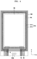
- FIG. 1 is a plan view schematically illustrating a display apparatus, according to an embodiment.
- a display apparatus 1 may provide an image through a plurality of sub-pixels P located in a display area DA.
- Each sub-pixel P may emit, for example, red light, green light, or blue light.
- each sub-pixel P may emit red light, green light, blue light, or white light.
- Each sub-pixel P may emit red light, green light, or blue light through a light-emitting diode.
- Each light-emitting diode may be electrically connected to a sub-pixel circuit including a transistor and a storage capacitor.
- Each sub-pixel circuit may be electrically connected to a scan line SL extending in the x-direction, and a data line DL extending in the y-direction crossing the scan line SL.
- a peripheral area PA is located outside the display area DA.
- the peripheral area PA may surround (e.g., around a periphery of) the display area DA.
- the peripheral area PA is a portion where the sub-pixels P are not located, and corresponds to a non-display area where an image is not provided.
- a first power voltage supply line 10 and a second power voltage supply line 20 may be located in the peripheral area PA.
- the first power voltage supply line 10 may be located to correspond to a first side E1 of the display area DA
- the second power voltage supply line 20 may be located to correspond to second, third, and fourth sides E2, E3, and E4 of the display area DA.
- FIG. 1 A first power voltage supply line 10 and a second power voltage supply line 20 may be located in the peripheral area PA.
- the first power voltage supply line 10 may be located to correspond to a first side E1 of the display area DA
- the second power voltage supply line 20 may be located to correspond to second, third, and fourth sides E2, E3, and E4 of the display area DA.
- the first power voltage supply line 10 is located between the first side E1 of the display area DA and a terminal unit (e.g., a terminal or terminal circuit) 30, and the second power voltage supply line 20 partially surrounds (e.g., around a periphery of) the display area DA in a loop shape with one open side, for example, such as in a loop shape in which a portion corresponding to the first side E1 is open.
- a terminal unit e.g., a terminal or terminal circuit
- the first power voltage supply line 10 includes a first body portion 11 extending along the first side E1 of the display area DA.
- the first body portion 11 may extend in the x-direction along the first side E1 of the display area DA, and may have a length equal to or greater than that of the first side E1.
- the first body portion 11 may be integrally formed with a first connecting portion 12 extending in the y-direction from the first body portion 11.
- the first connecting portion 12 may extend in the y-direction toward the terminal unit 30 in an inlet area POA.
- the inlet area POA is a portion of the peripheral area PA between the first side E1 of the display area DA adjacent to the terminal unit 30 and a side of the substrate 100, and may be a portion from the first side E1 of the display area DA to the terminal unit 30.
- the first connecting portion 12 may extend from the first body portion 11 toward an edge of the substrate 100, and may be connected to a first terminal 31 of the terminal unit 30.
- the second power voltage supply line 20 includes a second body portion 21 extending along the second to fourth sides E2, E3, and E4 of the display area DA.
- the second body portion 21 may partially surround (e.g., around a periphery of) the display area DA along the second to fourth sides E2, E3, and E4, except for the first side E1 of the display area DA.
- the second side E2 is located opposite to the first side E1, and the third and fourth sides E3 and E4 connect the first side E1 and the second side E2 to each other and are located opposite to each other.
- the second body portion 21 may surround (e.g., around at least a portion of a periphery of) the display area DA, and may surround (e.g., around a periphery of) opposite sides of the first body portion 11.
- the second body portion 21 may be integrally formed with a second connecting portion 22 extending in the y-direction from the second body portion 21.
- the second connecting portion 22 may extend in the y-direction toward the terminal unit 30 in the inlet area POA.
- the second connecting portion 22 may extend parallel to or substantially parallel to the first connecting portion 12 in the inlet area POA, and may be connected to a second terminal 32 of the terminal unit 30.
- the terminal unit 30 may correspond to an end portion of the substrate 100, may be exposed without being covered by an insulating layer or the like, and may be connected to a controller through a flexible printed circuit board or the like.
- a pad PAD may be located in the inlet area POA.
- the pads PAD may be spaced apart from each other in the inlet area POA.
- the pad PAD is an element to which an electronic device, for example, such as an integrated circuit (IC) chip or a printed circuit board including a data driver, is electrically connected.
- an anisotropic conductive film may be located between the pad PAD and the electronic device.
- the first power voltage supply line 10 may provide a first power voltage ELVDD (e.g., see FIG. 2 ) to each sub-pixel P
- the second power voltage supply line 20 may provide a second power voltage ELVSS (e.g., see FIG. 2 ) to each sub-pixel P.
- the first power voltage ELVDD of the first power voltage supply line 10 may be provided to a transistor corresponding to each sub-pixel P through a driving voltage line PL connected to the first power voltage supply line 10.
- the second power voltage ELVSS of the second power voltage supply line 20 may be provided to a second electrode (e.g., a cathode) of a light-emitting diode.
- the second body portion 21 of the second power voltage supply line 20 and the second electrode of the light-emitting diode may be connected to each other in the peripheral area PA to provide the second power voltage ELVSS.
- the display apparatus 1 for displaying a moving image and/or a still image may be used as a display screen for a portable electronic device, such as a mobile phone, a smartphone, a tablet personal computer (PC), a laptop computer, a mobile communication terminal, an electronic organizer, an electronic book, a portable multimedia player (PMP), a navigation device, or an ultra-mobile PC (UMPC), as well as for any of various suitable products, such as a television, a monitor, an advertisement board, or an Internet of things (IoT) product.
- the display apparatus 1 may be used in a wearable device, such as a smart watch, a watch phone, a glasses-type display, or a head-mounted display (HMD).
- the display apparatus 1 may be used as a center information display (CID) located on an instrument panel, a center fascia, or a dashboard of a vehicle, a mirror display used in a vehicle, or a display located on the back of a front seat for entertainment for a back seat of a vehicle.
- CID center information display
- FIG. 2 is an equivalent circuit diagram illustrating a light-emitting diode and a sub-pixel circuit corresponding to a sub-pixel of a display apparatus, according to an embodiment.
- the light-emitting diode is illustrated as an organic light-emitting diode OLED in FIG. 2 for convenience of illustration, the present disclosure is not limited thereto.
- the light-emitting diode may include any of various suitable kinds of light-emitting diodes, such as a diode including an inorganic material (e.g., a PN junction light-emitting diode), or a light-emitting diode including quantum dots.
- the light-emitting diode may be electrically connected to a transistor.
- the organic light-emitting diode OLED may be electrically connected to a sub-pixel circuit PC, and the sub-pixel circuit PC may include a first transistor T1, a second transistor T2, and a storage capacitor Cst.
- a first electrode (e.g., an anode) of the organic light-emitting diode OLED may be electrically connected to the first transistor T1
- a second electrode (e.g., a cathode) of the organic light-emitting diode OLED may be electrically connected to the second power voltage supply line 20 to receive a voltage corresponding to the second power voltage ELVSS.
- the second transistor T2 transmits a data signal Dm input through the data line DL according to a scan signal Sn input through the scan line SL to the first transistor T1.
- the storage capacitor Cst is connected to the second transistor T2 and the driving voltage line PL, and stores a voltage corresponding to a difference between a voltage received from the second transistor T2 and the first power voltage ELVDD supplied to the driving voltage line PL.
- the first transistor T1 may be connected to the driving voltage line PL and the storage capacitor Cst, and may control a driving current flowing through the organic light-emitting diode OLED from the driving voltage line PL in response to a value of the voltage stored in the storage capacitor Cst.
- the organic light-emitting diode OLED may emit light having a desired luminance (e.g., a certain or predetermined luminance) due to the driving current.
- sub-pixel circuit PC including two transistors and one storage capacitor is illustrated in FIG. 2 , the present disclosure is not limited thereto.
- the sub-pixel circuit of the display apparatus according to another embodiment may include three or more transistors and two or more capacitors.
- FIG. 3 is a cross-sectional view taken along the line III-III' of the display apparatus of FIG. 1 , according to an embodiment.
- the sub-pixel circuit PC including the first and second transistors T1 and T2 and the storage capacitor Cst may be located on the substrate 100, and the organic light-emitting diode OLED may be located on the sub-pixel circuit PC.
- the substrate 100 may include a glass material or a polymer resin.
- the polymer resin may include, for example, polyethersulfone (PES), polyacrylate (PAR), polyetherimide (PEI), polyethylene naphthalate (PEN), polyethylene terephthalate (PET), polyphenylene sulfide (PPS), polyarylate, polyimide (PI), polycarbonate (PC), or cellulose acetate propionate (CAP).
- the substrate 100 may have a single or multi-layered structure including one or more of the above materials, and the multi-layered structure may include a structure in which a polymer resin layer and a barrier layer including an inorganic insulating material are alternately stacked.
- the substrate 100 may be flexible, rollable, or bendable.
- a buffer layer 101 may be located on the substrate 100 to prevent or substantially prevent penetration of impurities.
- the buffer layer 101 may include silicon oxide, silicon oxynitride, and/or silicon nitride.
- the first transistor T1 includes a first semiconductor layer Act1 and a first gate electrode G1
- the second transistor T2 includes a second semiconductor layer Act2 and a second gate electrode G2.
- a first gate insulating layer 103 may be located between the first semiconductor layer Act1 and the first gate electrode G1, and between the second semiconductor layer Act2 and the second gate electrode G2.
- the first gate insulating layer 103 may include an inorganic insulating material, such as silicon oxide, silicon oxynitride, and/or silicon nitride, and may have a single or multi-layered structure.
- Each of the first semiconductor layer Act1 and the second semiconductor layer Act2 may include a silicon semiconductor such as polysilicon, an oxide semiconductor, or an organic semiconductor.
- the first semiconductor layer Act1 may include a first channel region C1 overlapping with the first gate electrode G1, and a first source region S1 and a first drain region D1 on opposite sides of the first channel region C1.
- the second semiconductor layer Act2 may include a second channel region C2 overlapping with the second gate electrode G2, and a second source region S2 and a second drain region D2 on opposite sides of the second channel region C2.
- the first gate electrode G1 and the second gate electrode G2 may be located on the first gate insulating layer 103 to overlap with the first channel region C1 and the second channel region C2, respectively.
- Each of the first gate electrode G1 and the second gate electrode G2 may include molybdenum (Mo), aluminum (Al), copper (Cu), or titanium (Ti), and may have a single or multi-layered structure.
- a source region and a drain region of a transistor may correspond to a source electrode and a drain electrode of the transistor, respectively.
- the first source region S1 and the first drain region D1 may be a first source electrode and a first drain electrode, respectively
- the second source region S2 and the second drain region D2 may be a second source electrode and a second drain electrode, respectively.
- the terms “source region” and “drain region” may be used instead of the terms “source electrode” and “drain electrode” for convenience.
- the storage capacitor Cst may overlap with the first transistor T1.
- the first gate electrode G1 may be a lower electrode CE1 of the storage capacitor Cst, and an upper electrode CE2 of the storage capacitor Cst may overlap with the lower electrode CE1.
- the upper electrode CE2 may include molybdenum (Mo), aluminum (Al), copper (Cu), or titanium (Ti), and may have a single or multi-layered structure.
- a second gate insulating layer 105 may be located between the lower electrode CE1 and the upper electrode CE2.
- the second gate insulating layer 105 may include silicon oxide, silicon oxynitride, and/or silicon nitride, and may have a single or multi-layered structure including one or more of the above materials.
- the first transistor T1, the second transistor T2, and the storage capacitor Cst may be covered by an interlayer insulating layer 107.
- the interlayer insulating layer 107 may include an inorganic insulating material, such as silicon oxide, silicon oxynitride, and/or silicon nitride.
- the data line DL is located on the interlayer insulating layer 107, and the data line DL is connected to the second semiconductor layer Act2 of the second transistor T2 through a contact hole passing through (e.g., penetrating) the first gate insulating layer 103, the second gate insulating layer 105 and the interlayer insulating layer 107.
- the data line DL is connected to the second drain region D2, and the data line DL may be the second drain electrode.
- the driving voltage line PL is located on the interlayer insulating layer 107.
- the driving voltage line PL may include a lower driving voltage line PL-1 and an upper driving voltage line PL-2.
- the driving voltage line PL may include the lower driving voltage line PL-1 and the upper driving voltage line PL-2 that are electrically connected to each other with a first insulating layer 109 therebetween, an increase in the resistance of the driving voltage line PL may be prevented or substantially prevented, and a voltage drop due to the resistance of the driving voltage line PL may be prevented or substantially prevented.
- the upper driving voltage line PL-2 may be electrically connected to the lower driving voltage line PL-1 via a contact hole in the first insulating layer 109.
- the lower driving voltage line PL-1 may include the same material as that of the data line DL.
- the lower driving voltage line PL-1 may include molybdenum (Mo), aluminum (Al), copper (Cu), or titanium (Ti), and may have a single or multi-layered structure.
- the lower driving voltage line PL-1 may have a multi-layered structure including Ti/Al/Ti.
- the lower driving voltage line PL-1 and the upper driving voltage line PL-2 may be connected to each other through a contact hole defined in (e.g., penetrating) the first insulating layer 109 located between the lower driving voltage line PL-1 and the upper driving voltage line PL-2, and the driving voltage line PL may be covered by a second insulating layer 111 that is a planarization insulating layer.
- the upper driving voltage line PL-2 may include molybdenum (Mo), aluminum (Al), copper (Cu), or titanium (Ti), and may have a single or multi-layered structure. In some embodiments, the upper driving voltage line PL-2 may have a multi-layered structure including Ti/Al/Ti.
- the first insulating layer 109 may include an inorganic insulating material and/or an organic insulating material.
- the first insulating layer 109 may include an organic insulating material, such as an imide-based polymer, a general-purpose polymer (e.g., polymethyl methacrylate (PMMA) or polystyrene (PS)), a polymer derivative having a phenol-based group, an acrylic-based polymer, an aryl ether-based polymer, an amide-based polymer, a fluorine-based polymer, a p-xylene-based polymer, a vinyl alcohol-based polymer, or a suitable blend thereof.
- PMMA polymethyl methacrylate
- PS polystyrene
- the second insulating layer 111 may be located between the sub-pixel circuit PC and a first electrode 310 of the organic light-emitting diode OLED.
- the second insulating layer 111 may include an organic insulating material.
- the second insulating layer 111 may include an imide-based polymer, a general-purpose polymer, such as polymethyl methacrylate (PMMA) or polystyrene (PS), a polymer derivative having a phenol-based group, an acrylic-based polymer, an aryl ether-based polymer, an amide-based polymer, a fluorine-based polymer, a p-xylene-based polymer, a vinyl alcohol-based polymer, or a suitable blend thereof.
- PMMA polymethyl methacrylate
- PS polystyrene
- a polymer derivative having a phenol-based group an acrylic-based polymer, an aryl ether-based polymer, an amide-based polymer, a fluorine-based
- the organic light-emitting diode OLED may have a stacked structure of the first electrode 310, an intermediate layer 320, and a second electrode 330.
- the first electrode 310 may be located on the second insulating layer 111.
- the first electrode 310 may include a metal and/or a conductive oxide.
- the first electrode 310 may include a reflective film including silver (Ag), magnesium (Mg), aluminum (Al), platinum (Pt), palladium (Pd), gold (Au), nickel (Ni), neodymium (Nd), iridium (Ir), chromium (Cr), or a suitable compound thereof, and a film formed of ITO, IZO, ZnO, or In 2 O 3 under and/or over the reflective film.
- the first electrode 310 may have a structure in which an ITO layer, a silver (Ag) layer, and an ITO layer are sequentially stacked.
- a bank layer 113 may cover an edge of the first electrode 310, and may include an opening overlapping with a part of the first electrode 310.
- the bank layer 215 may define a sub-pixel.
- a width of the opening of the bank layer 113 through which a top surface of the first electrode 310 is exposed may correspond to a width of an emission area where light is emitted, or in other words, a width of the sub-pixel.
- the bank layer 113 may include an insulating material.
- the bank layer 113 may include an organic insulating material, such as a general-purpose polymer (e.g., polymethyl methacrylate (PMMA) or polystyrene (PS)), a polymer derivative having a phenol-based group, an acrylic polymer, an imide-based polymer, an aryl ether-based polymer, an amide-based polymer, a fluorinated polymer, a p-xylene-based polymer, a vinyl alcohol-based polymer, or a suitable blend thereof.
- PMMA polymethyl methacrylate
- PS polystyrene
- the intermediate layer 320 includes an emission layer.
- the emission layer 320 may include a high molecular weight organic material or a low molecular weight organic material that emits light of a desired color (e.g., a certain or predetermined color).
- the intermediate layer 320 may include at least one functional layer.
- the at least one functional layer may include an organic material.
- the intermediate layer 320 may include a first functional layer between the emission layer and the first electrode 310, and/or a second functional layer between the emission layer and the second electrode 330.
- the first functional layer may have a single or multi-layered structure.
- the first functional layer when the first functional layer is formed of a high molecular weight material, the first functional layer may include a hole transport layer (HTL) having a single-layer structure.
- the first functional layer when the first functional layer is formed of a low molecular weight material, the first functional layer may include a hole injection layer (HIL) and a hole transport layer (HTL).
- HIL hole injection layer
- HTL hole transport layer
- the second functional layer may have a single or multi-layered structure.
- the second functional layer may include an electron transport layer (ETL) and/or an electron injection layer (EIL).
- ETL electron transport layer
- EIL electron injection layer
- the second electrode 330 may be formed of a conductive material having a low work function.
- the second electrode 330 may include a (semi-)transparent layer including silver (Ag), magnesium (Mg), aluminum (Al), platinum (Pt), palladium (Pd), gold (Au), nickel (Ni), neodymium (Nd), iridium (Ir), chromium (Cr), lithium (Li), calcium (Ca), or a suitable alloy thereof.
- the second electrode 330 may further include a layer formed of ITO, IZO, ZnO, or In 2 O 3 on the (semi-)transparent layer including one or more of the above materials.
- the second electrode 330 may include silver (Ag) and magnesium (Mg).
- the second electrode 330 may be formed to entirely cover the display area DA (e.g., see FIG. 1 ).
- the second electrode 330 is a common layer, and may cover a plurality of first electrodes 310.
- a thin-film encapsulation layer 400 may cover the organic light-emitting diode OLED.
- the thin-film encapsulation layer 400 may prevent or substantially prevent a light-emitting diode, such as the organic light-emitting diode OLED, from being damaged by external moisture and/or oxygen.
- the thin-film encapsulation layer 400 may include at least one organic encapsulation layer, and at least one inorganic encapsulation layer. In FIG.
- the thin-film encapsulation layer 400 is illustrated as including a first inorganic encapsulation layer 410, an organic encapsulation layer 420 on the first inorganic encapsulation layer 410, and a second inorganic encapsulation layer 430 on the organic encapsulation layer 420.
- the first inorganic encapsulation layer 410 may cover the second electrode 330, and may include silicon oxide, silicon nitride, and/or silicon oxynitride. In some embodiments, other layers, such as a capping layer, may be further located between the first inorganic encapsulation layer 410 and the second electrode 330 when necessary or desired. When the capping layer is not formed, the first inorganic encapsulation layer 410 may include at least two silicon oxynitride layers having different film qualities from one another.
- the organic encapsulation layer 420 may include at least one material selected from the group consisting of an acrylic-based resin, a methacrylic-based resin, polyisoprene-based resin, a vinyl-based resin, an epoxy-based resin, a urethane-based resin, a cellulose-based resin, and a perylene-based resin.
- the second inorganic encapsulation layer 430 may cover the organic encapsulation layer 420, and may include silicon oxide, silicon nitride, and/or silicon oxynitride.
- FIG. 4 is a plan view schematically illustrating a display apparatus, according to an embodiment.
- FIG. 4 illustrates the first power voltage supply line 10 and the second power voltage supply line 20 located in the peripheral area PA, and a partition wall 210 and the pad PAD located over the first and second power voltage supply lines 10 and 20.
- the first power voltage supply line 10, the second power voltage supply line 20, and the pad PAD may be the same or substantially the same as those described above with reference to FIG. 1 .
- the organic encapsulation layer 420 described above with reference to FIG. 3 may be formed by applying a monomer, and then curing the monomer.
- the partition wall 210 may prevent or substantially prevent the monomer from overflowing and traveling to the pad PAD in a process of applying the monomer.
- the partition wall 210 may include a first partition wall 212 and a second partition wall 214 that are spaced apart from each other as shown in FIG. 4 .
- Each of the first partition wall 212 and the second partition wall 214 may have a closed loop shape entirely surrounding (e.g., around a periphery of) the display area DA in a plan view as shown in FIG. 4 .
- FIG. 5 is an enlarged plan view illustrating the portion V of the display apparatus of FIG. 4 , according to an embodiment.
- FIG. 6 is a cross-sectional view taken along the line VI-VI' of FIG. 5 .
- FIG. 7 is a cross-sectional view taken along the line VII-VII' of FIG. 5 .
- FIG. 8 is a cross-sectional view taken along the line VIII-VIII' of FIG. 5 .
- FIG. 9 is a cross-sectional view taken along the line IX-IX' of FIG. 5.
- FIG. 5 may be a plan view illustrating a part of the inlet area POA described above with reference to FIG. 1 .
- a part of the first power voltage supply line 10 and a part of the second power voltage supply line 20 may cross the partition wall 210.
- each of the first connecting portion 12 of the first power voltage supply line 10 and the second connecting portion 22 of the second power voltage supply line 20 may extend in the y-direction in the inlet area POA, and the partition wall 210 may cross each of the first connecting portion 12 of the first power voltage supply line 10 and the second connecting portion 22 of the second power voltage supply line 20.
- the first partition wall 212 may cross the first connecting portion 12 of the first power voltage supply line 10 and the second connecting portion 22 of the second power voltage supply line 20.
- the second partition wall 214 may cross the first connecting portion 12 of the first power voltage supply line 10 and the second connecting portion 22 of the second power voltage supply line 20.
- Each of an edge 10E of the first power voltage supply line 10 and an edge 20E of the second power voltage supply line 20 may have an uneven structure in which a concave portion and a convex portion are alternately arranged in a plan view. Even when moisture penetrates from the peripheral area PA toward the display area DA (e.g., see FIG. 1 ) through the edge 10E of the first power voltage supply line 10 and/or the edge 20E of the second power voltage supply line 20, the traveling of the moisture may be delayed by the uneven structure of the edge 10E of the first power voltage supply line 10 and the edge 20E of the second power voltage supply line 20.
- the first power voltage supply line 10 and/or the second power voltage supply line 20 may have a stacked structure of conductive layers.
- the first power voltage supply line 10 and the second power voltage supply line 20 may have stacked structures including first conductive layers 10A and 20A, second conductive layers 10B and 20B on the first conductive layers 10A and 20A, and third conductive layers 10C and 20C on the second conductive layers 10B and 20B.
- the first conductive layer 10A, the second conductive layer 10B, and the third conductive layer 10C of the first power voltage supply line 10 may include the same materials as those of the first conductive layer 20A, the second conductive layer 20B, and the third conductive layer 20C of the second power voltage supply line 20.
- Insulating layers may be located between the substrate 100 and the first power voltage supply line 10, and between the substrate 100 and the second power voltage supply line 20.
- the buffer layer 101, the first gate insulating layer 103, the second gate insulating layer 105, and the interlayer insulating layer 107 are located between the substrate 100 and the first power voltage supply line 10, and between the substrate 100 and the second power voltage supply line 20.
- Each of the first conductive layers 10A and 20A, the second conductive layers 10B and 20B, and the third conductive layers 10C and 20C may include a conductive material, for example, such as a metal material.
- Each of the first conductive layers 10A and 20A, the second conductive layers 10B and 20B, and the third conductive layers 10C and 20C may include molybdenum (Mo), aluminum (Al), copper (Cu), or titanium (Ti), and may have a single or multi-layered structure.
- a metal included in the second conductive layers 10B and 20B may have an etch rate different from that of a metal included in the first conductive layers 10A and 20A and/or the third conductive layers 10C and 20C.
- the second conductive layers 10B and 20B may include aluminum
- the first conductive layers 10A and 20A and the third conductive layers 10C and 20C may include titanium, but the present disclosure is not limited thereto.
- a side shape (or a cross-sectional shape) of a portion of the first power voltage supply line 10 not overlapping with the partition wall 210 may be different from a side shape (or a cross-sectional shape) of a portion of the first power voltage supply line 10 overlapping with the partition wall 210.
- a side shape (or a cross-sectional shape) of a portion of the second power voltage supply line 20 not overlapping with the partition wall 210 may be different from a side shape (or a cross-sectional shape) of a portion of the second power voltage supply line 20 overlapping with the partition wall 210.
- a side surface of a portion 20-1 (hereinafter, referred to as a first portion) of the second power voltage supply line 20 not overlapping with the partition wall 210 may have a tip structure.
- a side surface of the first conductive layer 20A and a side surface of the third conductive layer 20C corresponding to the first portion 20-1 of the second power voltage supply line 20 are not located on the same plane as a side surface of the second conductive layer 20B.
- an end portion of the third conductive layer 20C corresponding to the first portion 20-1 of the second power voltage supply line 20 may include a tip PT protruding more laterally than the side surface of the second conductive layer 20B corresponding to the first portion 20-1 of the second power voltage supply line 20.
- the end portion of the third conductive layer 20C may include the tip PT further protruding in a lateral direction from a point where the side surface of the second conductive layer 20B and a bottom surface of the third conductive layer 20C meet each other.
- an end portion of the first conductive layer 20A corresponding to the first portion 20-1 of the second power voltage supply line 20 may include a tip PT protruding more laterally than the side surface of the second conductive layer 20B corresponding to the first portion 20-1 of the second power voltage supply line 20.
- the end portion of the first conductive layer 20A may include the tip PT further protruding in a lateral direction from a point where the side surface of the second conductive layer 20B and a top surface of the first conductive layer 20A meet each other.
- the second conductive layer 20B having an etch rate different from that of the first conductive layer 20A and the third conductive layer 20C may be etched more when the second power voltage supply line 20 is etched in a process of manufacturing a display apparatus, and thus, each of the first conductive layer 20A and the third conductive layer 20C may include the tip PT.
- the first inorganic encapsulation layer 410 may extend to the peripheral area PA, and may continuously cover the side surface of the first portion 20-1 of the second power voltage supply line 20 in the peripheral area PA.
- the first inorganic encapsulation layer 410 having relatively excellent step coverage may continuously cover the side surface of the first portion 20-1 of the second power voltage supply line 20 having the tip PT, but may not have a constant or substantially constant thickness (e.g., in the z-direction).
- a side surface of a portion 20-2 (hereinafter, referred to as a second portion) of the second power voltage supply line 20 overlapping with the partition wall 210, for example, such as the first partition wall 212, may have a gently inclined surface without including a tip.
- a side surface of the first conductive layer 20A, a side surface of the second conductive layer 20B, and a side surface of the third conductive layer 20C may be located on the same or substantially the same plane (e.g., the inclined surface) as each other.
- the side surface of the second power voltage supply line 20 under the partition wall 210, for example, such as the first partition wall 212 may have a forward tapered inclined surface without including a tip.
- a side surface of the first conductive layer 20A, a side surface of the second conductive layer 20B, and a side surface of the third conductive layer 20C may be located on the forward tapered inclined surface.
- the second portion 20-2 of the second power voltage supply line 20 may overlap with the first partition wall 212.
- a top surface and a side surface of the second portion 20-2 of the second power voltage supply line 20 may directly contact the first partition wall 212.
- the first partition wall 212 may include an organic insulating material, and the top surface and the side surface of the second portion 20-2 of the second power voltage supply line 20 may directly contact the organic insulating material of the first partition wall 212.
- a cavity e.g., an unnecessary cavity
- the partition wall 210 for example, such as the first partition wall 212, located on the second portion 20-2 of the second power voltage supply line 20 and the second portion 20-2 of the second power voltage supply line 20.
- a cavity e.g., an unnecessary cavity
- a side surface of the second portion 20-2 of the second power voltage supply line 20 has a gently inclined surface as shown in FIG.
- the cavity may not be formed, and the partition wall 210 may be prevented or substantially prevented from being separated or detached from the second portion 20-2 of the second power voltage supply line 20 due to the cavity.
- impurities may be prevented or substantially prevented from traveling through a cavity between the partition wall 210 and the second portion 20-2 of the second power voltage supply line 20, or from damaging a structure around the cavity.
- a decrease in the resistance of the second power voltage supply line 20 under the first partition wall 212 may be prevented or substantially prevented.
- FIG. 7 illustrates a cross-sectional structure of a portion of the second power voltage supply line 20 under the first partition wall 212
- the present disclosure is not limited thereto.
- a cross-sectional structure of a portion of the second power voltage supply line 20 under the second partition wall 214 may be the same or substantially the same as that shown in FIG. 7 .
- a side surface of a portion 10-1 (hereinafter, referred to as a first portion) of the first power voltage supply line 10 not overlapping with the partition wall 210 may have a tip structure.
- each of a side surface of the first conductive layer 10A and a side surface of the third conductive layer 10C corresponding to the first portion 10-1 of the first power voltage supply line 10 is not located on the same plane as a side surface of the second conductive layer 10B.
- an end portion of the third conductive layer 10C corresponding to the first portion 10-1 of the first power voltage supply line 10 may include a tip PT protruding more laterally than the side surface of the second conductive layer 10B corresponding to the first portion 10-1 of the first power voltage supply line 10.
- the end portion of the third conductive layer 10C may include the tip PT further protruding in a lateral direction from a point where the side surface of the second conductive layer 10B and a bottom surface of the third conductive layer 10C meet each other.
- an end portion of the first conductive layer 10A corresponding to the first portion 10-1 of the first power voltage supply line 10 may include a tip PT protruding more laterally than the side surface of the second conductive layer 10B corresponding to the first portion 10-1 of the first power voltage supply line 10.
- the end portion of the first conductive layer 10A may include the tip PT further protruding in a lateral direction from a point where the side surface of the second conductive layer 10B and a top surface of the first conductive layer 10A meet each other.
- the second conductive layer 10B having an etch rate different from that of the first conductive layer 10A and/or the third conductive layer 10C may be etched more when the first power voltage supply line 10 is etched in a process of manufacturing the display apparatus, and thus, each of the first conductive layer 10A and the third conductive layer 10C may include the tip PT.
- the first inorganic encapsulation layer 410 may extend to the peripheral area PA, and may continuously cover the side surface of the first portion 10-1 of the first power voltage supply line 10 in the peripheral area PA.
- the first inorganic encapsulation layer 410 having relatively excellent step coverage may continuously cover the side surface of the first portion 10-1 of the first power voltage supply line 10 having the tip PT, but may not have a constant or substantially constant thickness.
- a side surface of a portion 10-2 (hereinafter, referred to as a second portion) of the first power voltage supply line 10 overlapping with the partition wall 210, for example, such as the second partition wall 214, may have a gently inclined surface without including a tip.
- a side surface of the first conductive layer 10A, a side surface of the second conductive layer 10B, and a side surface of the third conductive layer 10C may be located on the same or substantially the same plane (e.g., the inclined surface) as each other.
- the side surface of the first power voltage supply line 10 under the partition wall 210, for example, such as the second partition wall 214 may have a forward tapered inclined surface without including a tip.
- the side surfaces of the first conductive layer 10A, the second conductive layer 10B, and the third conductive layer 10C may be located on the forward tapered inclined surface.
- the second portion 10-2 of the first power voltage supply line 10 may overlap with the second partition wall 214.
- a top surface and a side surface of the second portion 10-2 of the first power voltage supply line 10 may directly contact the second partition wall 214.
- the second partition wall 214 may include an organic insulating material, and the top surface and the side surface of the second portion 10-2 of the first power voltage supply line 10 may directly contact the organic insulating material of the second partition wall 214.
- a cavity e.g., an unnecessary cavity
- the partition wall 210 for example, such as the second partition wall 214, located on the second portion 10-2 of the first power voltage supply line 10 and the second portion 10-2 of the first power voltage supply line 10.
- a cavity e.g., an unnecessary cavity
- the side surface of the second portion 10-2 of the first power voltage supply line 10 has a gently inclined surface as shown in FIG.
- the cavity may not be formed, and the partition wall 210 may be prevented or substantially prevented from being separated or detached from the second portion 10-2 of the first power voltage supply line 10 due to the cavity.
- impurities may be prevented or substantially prevented from traveling through a cavity between the partition wall 210 and the second portion 10-2 of the first power voltage supply line 10, or from damaging a structure around the cavity.
- a decrease in the resistance of the first power voltage supply line 10 under the second partition wall 214 may be prevented or substantially prevented.
- FIG. 9 illustrates a cross-sectional structure of a portion of the first power voltage supply line 10 under the second partition wall 214
- the present disclosure is not limited thereto.
- a cross-sectional structure of a portion of the first power voltage supply line 10 under the first partition wall 212 may be the same or substantially the same as that shown in FIG. 9 .
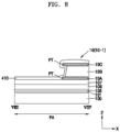
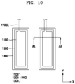
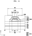
- FIG. 10 is a plan view illustrating a pad located in an inlet area of a display apparatus, according to an embodiment.
- FIG. 11 is a cross-sectional view taken along the line XI-XI' of FIG. 10 .
- the pad PAD may have a stacked structure of a plurality of pad layers. As shown in FIG. 10 , the pad PAD may include a first pad layer 1100, a second pad layer 1200 on the first pad layer 1100, and a third pad layer 1300 on the second pad layer 1200.
- a part 1100E (hereinafter, referred to as an extending portion) of the first pad layer 1100 may extend toward the display area DA (e.g., see FIG. 1 ), and may be electrically connected to a signal line (e.g., a data line) located in the display area DA.
- a signal line e.g., a data line
- a plurality of insulating layers may be located between the substrate 100 and the pad PAD.
- the buffer layer 101, the first gate insulating layer 103, the second gate insulating layer 105, and the interlayer insulating layer 107 are located between the substrate 100 and the pad PAD.
- a pad layer of the pad PAD may include the same material as that of the first power voltage supply line 10 (e.g., see FIG. 8 ) and/or the second power voltage supply line 20 (e.g., see FIG. 6 ).
- the first pad layer 1100 and/or the second pad layer 1200 may include the same material as that of the first power voltage supply line 10 and/or the second power voltage supply line 20, and may have the same stacked structure as that of the first power voltage supply line 10 and/or the second power voltage supply line 20.
- the first pad layer 1100 may have a stacked structure of a first sub-layer 1110, a second sub-layer 1120 on the first sub-layer 1110, and a third sub-layer 1130 on the second sub-layer 1120.
- the second pad layer 1200 may have a stacked structure of a first sub-layer 1210, a second sub-layer 1220 on the first sub-layer 1210, and a third sub-layer 1230 on the second sub-layer 1220.
- Each of the first sub-layers 1110 and 1210, the second sub-layers 1120 and 1220, and the third sub-layers 1130 and 1230 may include a conductive material, for example, such as a metal material.
- Each of the first sub-layers 1110 and 1210, the second sub-layers 1120 and 1220, and the third sub-layers 1130 and 1230 may include molybdenum (Mo), aluminum (Al), copper (Cu), or titanium (Ti), and may have a single or multi-layered structure.
- a metal included in the second sub-layers 1120 and 1220 may have an etch rate different from that of a metal included in the first sub-layers 1110 and 1210 and/or the third sub-layers 1130 and 1230.
- the first sub-layers 1110 and 1210, the second sub-layers 1120 and 1220, and the third sub-layers 1130 and 1230 may respectively include the same materials as those of the first conductive layers 10A and 20A (e.g., see FIGS. 6 and 8 ), the second conductive layers 10B and 20B (e.g., see FIGS. 6 and 8 ), and the third conductive layers 10C and 20C (e.g., see FIGS. 6 and 8 ) of the first power voltage supply line 10 and the second power voltage supply line 20.
- the second sub-layers 1120 and 1220 may include aluminum
- the first sub-layers 1110 and 1210 and the third sub-layers 1130 and 1230 may include titanium, but the present disclosure is not limited thereto.
- the first pad layer 1100 may have a side surface having a relatively gentle slope in a cross-sectional view.
- a side surface of the first sub-layer 1110, a side surface of the second sub-layer 1120, and a side surface of the third sub-layer 1130 may be located on the same or substantially the same plane, and may include a forward tapered inclined surface.
- Each of the end portions of the first sub-layer 1210 and the third sub-layer 1230 of the second pad layer 1200 may include a tip protruding more laterally than a side surface of the second sub-layer 1220.
- a width W2 of the second pad layer 1200 may be greater than a width W1 of the first pad layer 1100.
- the second pad layer 1200 may cover a side surface of the first pad layer 1100. For example, each of opposite side surfaces of the first pad layer 1100 in a width direction (e.g., the x-direction) may be covered by the second pad layer 1200.
- the second insulating layer 111 that is an organic insulating layer on the second pad layer 1200 may include an opening through which a part of a top surface of the second pad layer 1200 is exposed, and may cover opposite side surfaces of the second pad layer 1200 in the width direction. Because the second insulating layer 111 that is an organic insulating layer having a thickness greater than that of an inorganic insulating material covers opposite side surfaces of the second pad layer 1200, the influence of a tip structure of the second pad layer 1200 on a structure (e.g., a shape) of a surrounding layer, for example, such as the third pad layer 1300, in a process of forming the third pad layer 1300 may be minimized or reduced.
- a structure e.g., a shape
- a width W3 of the third pad layer 1300 may be greater than the width W2 of the second pad layer 1200.
- the third pad layer 1300 may directly contact a part of a top surface of the second pad layer 1200 exposed through an opening of the second insulating layer 111, and a part of a top surface of the second insulating layer 111.
- the third pad layer 1300 may be a single layer including a transparent conductive oxide, such as ITO.
- An anisotropic conductive film may be further located on the third pad layer 1300, and an electronic device, such as an IC chip, may be located on the anisotropic conductive film as described above with reference to FIG. 1 .
- an electronic device such as a flexible printed circuit board (FPCB), may be located on the third pad layer 1300.
- FPCB flexible printed circuit board
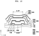
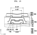
- FIGS. 12 through 14 are cross-sectional views illustrating a pad, according to one or more embodiments.
- the pad PAD may include the first pad layer 1100, the second pad layer 1200 on the first pad layer 1100, the third pad layer 1300 on the second pad layer 1200, and a lower pad layer 1000 under the first pad layer 1100.
- Each of the first pad layer 1100, the second pad layer 1200, and the third pad layer 1300 may have a stacked structure of a plurality of metal layers having different etch rates from one another.
- the first pad layer 1100, the second pad layer 1200, and the third pad layer 1300 may respectively include first sub-layers 1110, 1210, and 1310, second sub-layers 1120, 1220, and 1320, and third sub-layers 1130, 1230, and 1330.
- a metal of the first sub-layers 1110, 1210, and 1310 and/or the third sub-layers 1130, 1230, and 1330 may have an etch rate different from that of a metal of the second sub-layers 1120, 1220, and 1320.
- the first sub-layers 1110, 1210, and 1310 and/or the third sub-layers 1130, 1230, and 1330 may include titanium, and the second sub-layers 1120, 1220, and 1320 may include aluminum.
- the lower pad layer 1000 may include the same material as that of one of a gate electrode of a transistor or an electrode of a storage capacitor described above with reference to FIG. 3 .
- the lower pad layer 1000 may include molybdenum (Mo), aluminum (Al), copper (Cu), or titanium (Ti), and may have a single or multi-layered structure.
- the lower pad layer 1000 may be located on the second gate insulating layer 105.
- An edge of the lower pad layer 1000 may be covered by an inorganic insulating layer.
- an edge of the lower pad layer 1000 may be covered by the interlayer insulating layer 107, and the interlayer insulating layer 107 may include an opening 107OP through which a part of a top surface of the lower pad layer 1000 is exposed.
- the first pad layer 1100 may be electrically connected to the lower pad layer 1000 through the opening 107OP of the interlayer insulating layer 107.
- An insulating layer may not be located between the first pad layer 1100 and the second pad layer 1200.
- the second pad layer 1200 may overlap with and contact a top surface and a side surface of the first pad layer 1100.
- An insulating layer may be located on the second pad layer 1200, and the insulating layer may cover a side surface of the second pad layer 1200.
- an inorganic insulating layer IL may cover a side surface of the second pad layer 1200.
- the inorganic insulating layer IL may include a plurality of sub-inorganic insulating layers, and the plurality of sub-inorganic insulating layers may be a part of a thin-film encapsulation layer (e.g., a first inorganic encapsulation layer and/or a second inorganic encapsulation layer) and/or inorganic insulating layer(s) of a touch layer.
- the third pad layer 1300 may be located on the inorganic insulating layer IL.
- the third pad layer 1300 may be electrically connected to the second pad layer 1200 through an opening IL-OP of the inorganic insulating layer IL.
- the third pad layer 1300 may directly contact a part of a top surface of the second pad layer 1200 through the opening IL-OP of the inorganic insulating layer IL.
- a side surface of the third pad layer 1300 may not include a tip, unlike that of the second pad layer 1200.
- a side surface of the first sub-layer 1310, a side surface of the second sub-layer 1320, and a side surface of the third sub-layer 1330 corresponding to the side surface of the third pad layer 1300 may be located on the same or substantially the same plane.
- a side surface of the first sub-layer 1310 and/or a side surface of the third sub-layer 1330 of the third pad layer 1300 may protrude more than a side surface of the second sub-layer 1320.
- the pad PAD may include the first pad layer 1100, the second pad layer 1200 on the first pad layer 1100, the third pad layer 1300 on the second pad layer 1200, and the lower pad layer 1000 under the first pad layer 1100 as described above with reference to FIG. 12 .
- a stacked structure of an organic insulating layer OL and the inorganic insulating layer IL may be located on the second pad layer 1200, and the organic insulating layer OL and the inorganic insulating layer IL may respectively include openings OL-OP and IL-OP, each overlapping with a part of the second pad layer 1200.
- the organic insulating layer OL may be the second insulating layer 111 described above with reference to FIG. 11
- the inorganic insulating layer IL may be a part of a thin-film encapsulation layer (e.g., a first inorganic encapsulation layer and/or a second inorganic encapsulation layer) and/or inorganic insulating layer(s) of a touch layer.
- the third pad layer 1300 may directly contact a top surface of the second pad layer 1200 through the opening IL-OP of the inorganic insulating layer IL and the opening OL-OP of the organic insulating layer OL.
- the pad PAD may include the first pad layer 1100, the second pad layer 1200 on the first pad layer 1100, the third pad layer 1300 on the second pad layer 1200, and the lower pad layer 1000 under the first pad layer 1100.
- the stacked structure of the organic insulating layer OL and the inorganic insulating layer IL as described above with reference to FIG. 13 may be located between the second pad layer 1200 and the third pad layer 1300 of FIG. 14 .
- a width of the opening IL-OP of the inorganic insulating layer IL may be less than a width of the opening OL-OP of the organic insulating layer OL.
- An insulating layer may be located between the first pad layer 1100 and the second pad layer 1200 of the pad PAD. For example, a side surface of the first pad layer 1100 may overlap with and be covered by an additional inorganic insulating layer 108.
- the additional inorganic insulating layer 108 may be located on the interlayer insulating layer 107, and may include an inorganic insulating material, such as silicon oxide, silicon oxynitride, and/or silicon nitride.
- the additional inorganic insulating layer 108 may include an opening 108OP overlapping with a part of the first pad layer 1100.
- a width of the opening 108OP of the additional inorganic insulating layer 108 may be greater than a width of the opening 107OP of the interlayer insulating layer 107.
- the second pad layer 1200 may directly contact a top surface of the first pad layer 1100 through the opening 108OP of the additional inorganic insulating layer 108.
- a display apparatus may be provided, in which defects caused by a shape of a power voltage supply line and/or a pad are minimized or reduced, and thus, damage caused by external impurities such as moisture during or after manufacture may be minimized or reduced.
- defects caused by a shape of a power voltage supply line and/or a pad are minimized or reduced, and thus, damage caused by external impurities such as moisture during or after manufacture may be minimized or reduced.
- the aspects and features of the present disclosure are not limited thereto.
Landscapes
- Engineering & Computer Science (AREA)
- Microelectronics & Electronic Packaging (AREA)
- Electroluminescent Light Sources (AREA)
- Devices For Indicating Variable Information By Combining Individual Elements (AREA)
Applications Claiming Priority (2)
| Application Number | Priority Date | Filing Date | Title |
|---|---|---|---|
| KR20230039099 | 2023-03-24 | ||
| KR1020230050246A KR20240144615A (ko) | 2023-03-24 | 2023-04-17 | 표시 장치 |
Publications (1)
| Publication Number | Publication Date |
|---|---|
| EP4440283A1 true EP4440283A1 (de) | 2024-10-02 |
Family
ID=90417439
Family Applications (1)
| Application Number | Title | Priority Date | Filing Date |
|---|---|---|---|
| EP24165073.8A Pending EP4440283A1 (de) | 2023-03-24 | 2024-03-21 | Anzeigegerät |
Country Status (2)
| Country | Link |
|---|---|
| US (1) | US20240324361A1 (de) |
| EP (1) | EP4440283A1 (de) |
Citations (4)
| Publication number | Priority date | Publication date | Assignee | Title |
|---|---|---|---|---|
| US20190288234A1 (en) * | 2018-03-16 | 2019-09-19 | Samsung Display Co., Ltd. | Display device including a barrier layer |
| US20200381653A1 (en) * | 2019-05-28 | 2020-12-03 | Samsung Display Co., Ltd. | Display apparatus |
| US20200395428A1 (en) * | 2019-06-13 | 2020-12-17 | Samsung Display Co., Ltd. | Display device |
| US20220013614A1 (en) * | 2020-07-07 | 2022-01-13 | Samsung Display Co, Ltd. | Display apparatus |
-
2024
- 2024-03-18 US US18/608,750 patent/US20240324361A1/en active Pending
- 2024-03-21 EP EP24165073.8A patent/EP4440283A1/de active Pending
Patent Citations (4)
| Publication number | Priority date | Publication date | Assignee | Title |
|---|---|---|---|---|
| US20190288234A1 (en) * | 2018-03-16 | 2019-09-19 | Samsung Display Co., Ltd. | Display device including a barrier layer |
| US20200381653A1 (en) * | 2019-05-28 | 2020-12-03 | Samsung Display Co., Ltd. | Display apparatus |
| US20200395428A1 (en) * | 2019-06-13 | 2020-12-17 | Samsung Display Co., Ltd. | Display device |
| US20220013614A1 (en) * | 2020-07-07 | 2022-01-13 | Samsung Display Co, Ltd. | Display apparatus |
Also Published As
| Publication number | Publication date |
|---|---|
| US20240324361A1 (en) | 2024-09-26 |
Similar Documents
| Publication | Publication Date | Title |
|---|---|---|
| US20260111089A1 (en) | Touch sensing unit and display device including the same | |
| US12082469B2 (en) | Display apparatus and method of manufacturing the same | |
| US20220263046A1 (en) | Display apparatus | |
| US12586519B2 (en) | Display apparatus and method of manufacturing the same | |
| EP4326034A1 (de) | Anzeigevorrichtung und verfahren zur herstellung davon | |
| CN117956841A (zh) | 显示设备及其制造方法 | |
| CN117651445A (zh) | 显示装置 | |
| KR102792576B1 (ko) | 표시 장치 및 이를 구비한 전자 기기 | |
| US12568742B2 (en) | Display panel and electronic device including same | |
| US20240049508A1 (en) | Display device and method of manufacturing the same | |
| US20240049572A1 (en) | Display panel and electronic device including the same | |
| EP4440283A1 (de) | Anzeigegerät | |
| CN114628460A (zh) | 显示装置 | |
| CN118695674A (zh) | 显示装置 | |
| KR20240144615A (ko) | 표시 장치 | |
| US12547288B2 (en) | Display device | |
| US20240099082A1 (en) | Display apparatus | |
| CN222424630U (zh) | 显示装置 | |
| US20240324315A1 (en) | Display apparatus and method of manufacturing the same | |
| US12471460B2 (en) | Display apparatus including a pad at a non-display area overlapping with a conductor connecting a conductive line to the pad | |
| US20250241175A1 (en) | Display Device | |
| US20240237437A1 (en) | Display apparatus | |
| US20240099075A1 (en) | Display device | |
| US20240065055A1 (en) | Display apparatus | |
| US20240237459A1 (en) | Display apparatus |
Legal Events
| Date | Code | Title | Description |
|---|---|---|---|
| PUAI | Public reference made under article 153(3) epc to a published international application that has entered the european phase |
Free format text: ORIGINAL CODE: 0009012 |
|
| STAA | Information on the status of an ep patent application or granted ep patent |
Free format text: STATUS: THE APPLICATION HAS BEEN PUBLISHED |
|
| AK | Designated contracting states |
Kind code of ref document: A1 Designated state(s): AL AT BE BG CH CY CZ DE DK EE ES FI FR GB GR HR HU IE IS IT LI LT LU LV MC ME MK MT NL NO PL PT RO RS SE SI SK SM TR |
|
| STAA | Information on the status of an ep patent application or granted ep patent |
Free format text: STATUS: REQUEST FOR EXAMINATION WAS MADE |
|
| 17P | Request for examination filed |
Effective date: 20250328 |
|
| P01 | Opt-out of the competence of the unified patent court (upc) registered |
Free format text: CASE NUMBER: UPC_APP_0007399_4440283/2026 Effective date: 20260226 |