EP4440253A2 - High density organic bridge device and method - Google Patents
High density organic bridge device and method Download PDFInfo
- Publication number
- EP4440253A2 EP4440253A2 EP24186432.1A EP24186432A EP4440253A2 EP 4440253 A2 EP4440253 A2 EP 4440253A2 EP 24186432 A EP24186432 A EP 24186432A EP 4440253 A2 EP4440253 A2 EP 4440253A2
- Authority
- EP
- European Patent Office
- Prior art keywords
- metal pad
- bridge
- layer
- substrate
- die
- Prior art date
- Legal status (The legal status is an assumption and is not a legal conclusion. Google has not performed a legal analysis and makes no representation as to the accuracy of the status listed.)
- Pending
Links
Images


Classifications
-
- H—ELECTRICITY
- H10—SEMICONDUCTOR DEVICES; ELECTRIC SOLID-STATE DEVICES NOT OTHERWISE PROVIDED FOR
- H10W—GENERIC PACKAGES, INTERCONNECTIONS, CONNECTORS OR OTHER CONSTRUCTIONAL DETAILS OF DEVICES COVERED BY CLASS H10
- H10W72/00—Interconnections or connectors in packages
-
- H—ELECTRICITY
- H05—ELECTRIC TECHNIQUES NOT OTHERWISE PROVIDED FOR
- H05K—PRINTED CIRCUITS; CASINGS OR CONSTRUCTIONAL DETAILS OF ELECTRIC APPARATUS; MANUFACTURE OF ASSEMBLAGES OF ELECTRICAL COMPONENTS
- H05K1/00—Printed circuits
- H05K1/02—Details
- H05K1/14—Structural association of two or more printed circuits
- H05K1/141—One or more single auxiliary printed circuits mounted on a main printed circuit, e.g. modules, adapters
-
- H—ELECTRICITY
- H10—SEMICONDUCTOR DEVICES; ELECTRIC SOLID-STATE DEVICES NOT OTHERWISE PROVIDED FOR
- H10P—GENERIC PROCESSES OR APPARATUS FOR THE MANUFACTURE OR TREATMENT OF DEVICES COVERED BY CLASS H10
- H10P72/00—Handling or holding of wafers, substrates or devices during manufacture or treatment thereof
- H10P72/70—Handling or holding of wafers, substrates or devices during manufacture or treatment thereof for supporting or gripping
- H10P72/74—Handling or holding of wafers, substrates or devices during manufacture or treatment thereof for supporting or gripping using temporarily an auxiliary support
-
- H—ELECTRICITY
- H10—SEMICONDUCTOR DEVICES; ELECTRIC SOLID-STATE DEVICES NOT OTHERWISE PROVIDED FOR
- H10W—GENERIC PACKAGES, INTERCONNECTIONS, CONNECTORS OR OTHER CONSTRUCTIONAL DETAILS OF DEVICES COVERED BY CLASS H10
- H10W70/00—Package substrates; Interposers; Redistribution layers [RDL]
- H10W70/01—Manufacture or treatment
- H10W70/05—Manufacture or treatment of insulating or insulated package substrates, or of interposers, or of redistribution layers
-
- H—ELECTRICITY
- H10—SEMICONDUCTOR DEVICES; ELECTRIC SOLID-STATE DEVICES NOT OTHERWISE PROVIDED FOR
- H10W—GENERIC PACKAGES, INTERCONNECTIONS, CONNECTORS OR OTHER CONSTRUCTIONAL DETAILS OF DEVICES COVERED BY CLASS H10
- H10W70/00—Package substrates; Interposers; Redistribution layers [RDL]
- H10W70/01—Manufacture or treatment
- H10W70/05—Manufacture or treatment of insulating or insulated package substrates, or of interposers, or of redistribution layers
- H10W70/093—Connecting or disconnecting other interconnections thereto or therefrom, e.g. connecting bond wires or bumps
-
- H—ELECTRICITY
- H10—SEMICONDUCTOR DEVICES; ELECTRIC SOLID-STATE DEVICES NOT OTHERWISE PROVIDED FOR
- H10W—GENERIC PACKAGES, INTERCONNECTIONS, CONNECTORS OR OTHER CONSTRUCTIONAL DETAILS OF DEVICES COVERED BY CLASS H10
- H10W70/00—Package substrates; Interposers; Redistribution layers [RDL]
- H10W70/01—Manufacture or treatment
- H10W70/05—Manufacture or treatment of insulating or insulated package substrates, or of interposers, or of redistribution layers
- H10W70/095—Manufacture or treatment of insulating or insulated package substrates, or of interposers, or of redistribution layers of vias therein
-
- H—ELECTRICITY
- H10—SEMICONDUCTOR DEVICES; ELECTRIC SOLID-STATE DEVICES NOT OTHERWISE PROVIDED FOR
- H10W—GENERIC PACKAGES, INTERCONNECTIONS, CONNECTORS OR OTHER CONSTRUCTIONAL DETAILS OF DEVICES COVERED BY CLASS H10
- H10W70/00—Package substrates; Interposers; Redistribution layers [RDL]
- H10W70/60—Insulating or insulated package substrates; Interposers; Redistribution layers
-
- H—ELECTRICITY
- H10—SEMICONDUCTOR DEVICES; ELECTRIC SOLID-STATE DEVICES NOT OTHERWISE PROVIDED FOR
- H10W—GENERIC PACKAGES, INTERCONNECTIONS, CONNECTORS OR OTHER CONSTRUCTIONAL DETAILS OF DEVICES COVERED BY CLASS H10
- H10W70/00—Package substrates; Interposers; Redistribution layers [RDL]
- H10W70/60—Insulating or insulated package substrates; Interposers; Redistribution layers
- H10W70/611—Insulating or insulated package substrates; Interposers; Redistribution layers for connecting multiple chips together
-
- H—ELECTRICITY
- H10—SEMICONDUCTOR DEVICES; ELECTRIC SOLID-STATE DEVICES NOT OTHERWISE PROVIDED FOR
- H10W—GENERIC PACKAGES, INTERCONNECTIONS, CONNECTORS OR OTHER CONSTRUCTIONAL DETAILS OF DEVICES COVERED BY CLASS H10
- H10W70/00—Package substrates; Interposers; Redistribution layers [RDL]
- H10W70/60—Insulating or insulated package substrates; Interposers; Redistribution layers
- H10W70/611—Insulating or insulated package substrates; Interposers; Redistribution layers for connecting multiple chips together
- H10W70/616—Insulating or insulated package substrates; Interposers; Redistribution layers for connecting multiple chips together package substrates, interposers or redistribution layers combined with bridge chips
- H10W70/618—Insulating or insulated package substrates; Interposers; Redistribution layers for connecting multiple chips together package substrates, interposers or redistribution layers combined with bridge chips the bridge chips being embedded in the package substrates, interposers or redistribution layers
-
- H—ELECTRICITY
- H10—SEMICONDUCTOR DEVICES; ELECTRIC SOLID-STATE DEVICES NOT OTHERWISE PROVIDED FOR
- H10W—GENERIC PACKAGES, INTERCONNECTIONS, CONNECTORS OR OTHER CONSTRUCTIONAL DETAILS OF DEVICES COVERED BY CLASS H10
- H10W70/00—Package substrates; Interposers; Redistribution layers [RDL]
- H10W70/60—Insulating or insulated package substrates; Interposers; Redistribution layers
- H10W70/62—Insulating or insulated package substrates; Interposers; Redistribution layers characterised by their interconnections
- H10W70/63—Vias, e.g. via plugs
- H10W70/635—Through-vias
-
- H—ELECTRICITY
- H10—SEMICONDUCTOR DEVICES; ELECTRIC SOLID-STATE DEVICES NOT OTHERWISE PROVIDED FOR
- H10W—GENERIC PACKAGES, INTERCONNECTIONS, CONNECTORS OR OTHER CONSTRUCTIONAL DETAILS OF DEVICES COVERED BY CLASS H10
- H10W70/00—Package substrates; Interposers; Redistribution layers [RDL]
- H10W70/60—Insulating or insulated package substrates; Interposers; Redistribution layers
- H10W70/62—Insulating or insulated package substrates; Interposers; Redistribution layers characterised by their interconnections
- H10W70/65—Shapes or dispositions of interconnections
-
- H—ELECTRICITY
- H10—SEMICONDUCTOR DEVICES; ELECTRIC SOLID-STATE DEVICES NOT OTHERWISE PROVIDED FOR
- H10W—GENERIC PACKAGES, INTERCONNECTIONS, CONNECTORS OR OTHER CONSTRUCTIONAL DETAILS OF DEVICES COVERED BY CLASS H10
- H10W70/00—Package substrates; Interposers; Redistribution layers [RDL]
- H10W70/60—Insulating or insulated package substrates; Interposers; Redistribution layers
- H10W70/62—Insulating or insulated package substrates; Interposers; Redistribution layers characterised by their interconnections
- H10W70/66—Conductive materials thereof
-
- H—ELECTRICITY
- H10—SEMICONDUCTOR DEVICES; ELECTRIC SOLID-STATE DEVICES NOT OTHERWISE PROVIDED FOR
- H10W—GENERIC PACKAGES, INTERCONNECTIONS, CONNECTORS OR OTHER CONSTRUCTIONAL DETAILS OF DEVICES COVERED BY CLASS H10
- H10W70/00—Package substrates; Interposers; Redistribution layers [RDL]
- H10W70/60—Insulating or insulated package substrates; Interposers; Redistribution layers
- H10W70/67—Insulating or insulated package substrates; Interposers; Redistribution layers characterised by their insulating layers or insulating parts
- H10W70/68—Shapes or dispositions thereof
-
- H—ELECTRICITY
- H10—SEMICONDUCTOR DEVICES; ELECTRIC SOLID-STATE DEVICES NOT OTHERWISE PROVIDED FOR
- H10W—GENERIC PACKAGES, INTERCONNECTIONS, CONNECTORS OR OTHER CONSTRUCTIONAL DETAILS OF DEVICES COVERED BY CLASS H10
- H10W70/00—Package substrates; Interposers; Redistribution layers [RDL]
- H10W70/60—Insulating or insulated package substrates; Interposers; Redistribution layers
- H10W70/67—Insulating or insulated package substrates; Interposers; Redistribution layers characterised by their insulating layers or insulating parts
- H10W70/68—Shapes or dispositions thereof
- H10W70/685—Shapes or dispositions thereof comprising multiple insulating layers
-
- H—ELECTRICITY
- H10—SEMICONDUCTOR DEVICES; ELECTRIC SOLID-STATE DEVICES NOT OTHERWISE PROVIDED FOR
- H10W—GENERIC PACKAGES, INTERCONNECTIONS, CONNECTORS OR OTHER CONSTRUCTIONAL DETAILS OF DEVICES COVERED BY CLASS H10
- H10W70/00—Package substrates; Interposers; Redistribution layers [RDL]
- H10W70/60—Insulating or insulated package substrates; Interposers; Redistribution layers
- H10W70/67—Insulating or insulated package substrates; Interposers; Redistribution layers characterised by their insulating layers or insulating parts
- H10W70/69—Insulating materials thereof
-
- H—ELECTRICITY
- H10—SEMICONDUCTOR DEVICES; ELECTRIC SOLID-STATE DEVICES NOT OTHERWISE PROVIDED FOR
- H10W—GENERIC PACKAGES, INTERCONNECTIONS, CONNECTORS OR OTHER CONSTRUCTIONAL DETAILS OF DEVICES COVERED BY CLASS H10
- H10W70/00—Package substrates; Interposers; Redistribution layers [RDL]
- H10W70/60—Insulating or insulated package substrates; Interposers; Redistribution layers
- H10W70/67—Insulating or insulated package substrates; Interposers; Redistribution layers characterised by their insulating layers or insulating parts
- H10W70/69—Insulating materials thereof
- H10W70/695—Organic materials
-
- H—ELECTRICITY
- H10—SEMICONDUCTOR DEVICES; ELECTRIC SOLID-STATE DEVICES NOT OTHERWISE PROVIDED FOR
- H10W—GENERIC PACKAGES, INTERCONNECTIONS, CONNECTORS OR OTHER CONSTRUCTIONAL DETAILS OF DEVICES COVERED BY CLASS H10
- H10W90/00—Package configurations
-
- H—ELECTRICITY
- H10—SEMICONDUCTOR DEVICES; ELECTRIC SOLID-STATE DEVICES NOT OTHERWISE PROVIDED FOR
- H10W—GENERIC PACKAGES, INTERCONNECTIONS, CONNECTORS OR OTHER CONSTRUCTIONAL DETAILS OF DEVICES COVERED BY CLASS H10
- H10W90/00—Package configurations
- H10W90/401—Package configurations characterised by multiple insulating or insulated package substrates, interposers or RDLs
-
- H—ELECTRICITY
- H10—SEMICONDUCTOR DEVICES; ELECTRIC SOLID-STATE DEVICES NOT OTHERWISE PROVIDED FOR
- H10W—GENERIC PACKAGES, INTERCONNECTIONS, CONNECTORS OR OTHER CONSTRUCTIONAL DETAILS OF DEVICES COVERED BY CLASS H10
- H10W90/00—Package configurations
- H10W90/701—Package configurations characterised by the relative positions of pads or connectors relative to package parts
-
- H—ELECTRICITY
- H05—ELECTRIC TECHNIQUES NOT OTHERWISE PROVIDED FOR
- H05K—PRINTED CIRCUITS; CASINGS OR CONSTRUCTIONAL DETAILS OF ELECTRIC APPARATUS; MANUFACTURE OF ASSEMBLAGES OF ELECTRICAL COMPONENTS
- H05K1/00—Printed circuits
- H05K1/02—Details
- H05K1/03—Use of materials for the substrate
- H05K1/0313—Organic insulating material
-
- H—ELECTRICITY
- H05—ELECTRIC TECHNIQUES NOT OTHERWISE PROVIDED FOR
- H05K—PRINTED CIRCUITS; CASINGS OR CONSTRUCTIONAL DETAILS OF ELECTRIC APPARATUS; MANUFACTURE OF ASSEMBLAGES OF ELECTRICAL COMPONENTS
- H05K1/00—Printed circuits
- H05K1/02—Details
- H05K1/14—Structural association of two or more printed circuits
- H05K1/142—Arrangements of planar printed circuit boards in the same plane, e.g. auxiliary printed circuit insert mounted in a main printed circuit
-
- H—ELECTRICITY
- H05—ELECTRIC TECHNIQUES NOT OTHERWISE PROVIDED FOR
- H05K—PRINTED CIRCUITS; CASINGS OR CONSTRUCTIONAL DETAILS OF ELECTRIC APPARATUS; MANUFACTURE OF ASSEMBLAGES OF ELECTRICAL COMPONENTS
- H05K1/00—Printed circuits
- H05K1/18—Printed circuits structurally associated with non-printed electric components
- H05K1/181—Printed circuits structurally associated with non-printed electric components associated with surface mounted components
-
- H—ELECTRICITY
- H05—ELECTRIC TECHNIQUES NOT OTHERWISE PROVIDED FOR
- H05K—PRINTED CIRCUITS; CASINGS OR CONSTRUCTIONAL DETAILS OF ELECTRIC APPARATUS; MANUFACTURE OF ASSEMBLAGES OF ELECTRICAL COMPONENTS
- H05K2201/00—Indexing scheme relating to printed circuits covered by H05K1/00
- H05K2201/04—Assemblies of printed circuits
- H05K2201/048—Second PCB mounted on first PCB by inserting in window or holes of the first PCB
-
- H—ELECTRICITY
- H05—ELECTRIC TECHNIQUES NOT OTHERWISE PROVIDED FOR
- H05K—PRINTED CIRCUITS; CASINGS OR CONSTRUCTIONAL DETAILS OF ELECTRIC APPARATUS; MANUFACTURE OF ASSEMBLAGES OF ELECTRICAL COMPONENTS
- H05K2201/00—Indexing scheme relating to printed circuits covered by H05K1/00
- H05K2201/04—Assemblies of printed circuits
- H05K2201/049—PCB for one component, e.g. for mounting onto mother PCB
-
- H—ELECTRICITY
- H05—ELECTRIC TECHNIQUES NOT OTHERWISE PROVIDED FOR
- H05K—PRINTED CIRCUITS; CASINGS OR CONSTRUCTIONAL DETAILS OF ELECTRIC APPARATUS; MANUFACTURE OF ASSEMBLAGES OF ELECTRICAL COMPONENTS
- H05K2201/00—Indexing scheme relating to printed circuits covered by H05K1/00
- H05K2201/10—Details of components or other objects attached to or integrated in a printed circuit board
- H05K2201/10431—Details of mounted components
- H05K2201/10507—Involving several components
- H05K2201/10522—Adjacent components
-
- H—ELECTRICITY
- H05—ELECTRIC TECHNIQUES NOT OTHERWISE PROVIDED FOR
- H05K—PRINTED CIRCUITS; CASINGS OR CONSTRUCTIONAL DETAILS OF ELECTRIC APPARATUS; MANUFACTURE OF ASSEMBLAGES OF ELECTRICAL COMPONENTS
- H05K2201/00—Indexing scheme relating to printed circuits covered by H05K1/00
- H05K2201/10—Details of components or other objects attached to or integrated in a printed circuit board
- H05K2201/10613—Details of electrical connections of non-printed components, e.g. special leads
- H05K2201/10621—Components characterised by their electrical contacts
- H05K2201/10674—Flip chip
-
- H—ELECTRICITY
- H05—ELECTRIC TECHNIQUES NOT OTHERWISE PROVIDED FOR
- H05K—PRINTED CIRCUITS; CASINGS OR CONSTRUCTIONAL DETAILS OF ELECTRIC APPARATUS; MANUFACTURE OF ASSEMBLAGES OF ELECTRICAL COMPONENTS
- H05K2203/00—Indexing scheme relating to apparatus or processes for manufacturing printed circuits covered by H05K3/00
- H05K2203/01—Tools for processing; Objects used during processing
- H05K2203/0147—Carriers and holders
- H05K2203/016—Temporary inorganic, non-metallic carrier, e.g. for processing or transferring
-
- H—ELECTRICITY
- H05—ELECTRIC TECHNIQUES NOT OTHERWISE PROVIDED FOR
- H05K—PRINTED CIRCUITS; CASINGS OR CONSTRUCTIONAL DETAILS OF ELECTRIC APPARATUS; MANUFACTURE OF ASSEMBLAGES OF ELECTRICAL COMPONENTS
- H05K3/00—Apparatus or processes for manufacturing printed circuits
- H05K3/30—Assembling printed circuits with electric components, e.g. with resistors
- H05K3/32—Assembling printed circuits with electric components, e.g. with resistors electrically connecting electric components or wires to printed circuits
- H05K3/34—Assembling printed circuits with electric components, e.g. with resistors electrically connecting electric components or wires to printed circuits by soldering
- H05K3/341—Surface mounted components
- H05K3/3431—Leadless components
- H05K3/3436—Leadless components having an array of bottom contacts, e.g. pad grid array or ball grid array components
-
- H—ELECTRICITY
- H05—ELECTRIC TECHNIQUES NOT OTHERWISE PROVIDED FOR
- H05K—PRINTED CIRCUITS; CASINGS OR CONSTRUCTIONAL DETAILS OF ELECTRIC APPARATUS; MANUFACTURE OF ASSEMBLAGES OF ELECTRICAL COMPONENTS
- H05K3/00—Apparatus or processes for manufacturing printed circuits
- H05K3/46—Manufacturing multilayer circuits
- H05K3/4644—Manufacturing multilayer circuits by building the multilayer layer by layer, i.e. build-up multilayer circuits
- H05K3/467—Adding a circuit layer by thin film methods
-
- H—ELECTRICITY
- H10—SEMICONDUCTOR DEVICES; ELECTRIC SOLID-STATE DEVICES NOT OTHERWISE PROVIDED FOR
- H10P—GENERIC PROCESSES OR APPARATUS FOR THE MANUFACTURE OR TREATMENT OF DEVICES COVERED BY CLASS H10
- H10P72/00—Handling or holding of wafers, substrates or devices during manufacture or treatment thereof
- H10P72/70—Handling or holding of wafers, substrates or devices during manufacture or treatment thereof for supporting or gripping
- H10P72/74—Handling or holding of wafers, substrates or devices during manufacture or treatment thereof for supporting or gripping using temporarily an auxiliary support
- H10P72/7424—Handling or holding of wafers, substrates or devices during manufacture or treatment thereof for supporting or gripping using temporarily an auxiliary support used as a support during the manufacture of self-supporting substrates
-
- H—ELECTRICITY
- H10—SEMICONDUCTOR DEVICES; ELECTRIC SOLID-STATE DEVICES NOT OTHERWISE PROVIDED FOR
- H10W—GENERIC PACKAGES, INTERCONNECTIONS, CONNECTORS OR OTHER CONSTRUCTIONAL DETAILS OF DEVICES COVERED BY CLASS H10
- H10W70/00—Package substrates; Interposers; Redistribution layers [RDL]
- H10W70/60—Insulating or insulated package substrates; Interposers; Redistribution layers
- H10W70/62—Insulating or insulated package substrates; Interposers; Redistribution layers characterised by their interconnections
- H10W70/63—Vias, e.g. via plugs
-
- H—ELECTRICITY
- H10—SEMICONDUCTOR DEVICES; ELECTRIC SOLID-STATE DEVICES NOT OTHERWISE PROVIDED FOR
- H10W—GENERIC PACKAGES, INTERCONNECTIONS, CONNECTORS OR OTHER CONSTRUCTIONAL DETAILS OF DEVICES COVERED BY CLASS H10
- H10W72/00—Interconnections or connectors in packages
- H10W72/071—Connecting or disconnecting
- H10W72/072—Connecting or disconnecting of bump connectors
-
- H—ELECTRICITY
- H10—SEMICONDUCTOR DEVICES; ELECTRIC SOLID-STATE DEVICES NOT OTHERWISE PROVIDED FOR
- H10W—GENERIC PACKAGES, INTERCONNECTIONS, CONNECTORS OR OTHER CONSTRUCTIONAL DETAILS OF DEVICES COVERED BY CLASS H10
- H10W72/00—Interconnections or connectors in packages
- H10W72/071—Connecting or disconnecting
- H10W72/072—Connecting or disconnecting of bump connectors
- H10W72/07231—Techniques
- H10W72/07232—Compression bonding, e.g. thermocompression bonding
-
- H—ELECTRICITY
- H10—SEMICONDUCTOR DEVICES; ELECTRIC SOLID-STATE DEVICES NOT OTHERWISE PROVIDED FOR
- H10W—GENERIC PACKAGES, INTERCONNECTIONS, CONNECTORS OR OTHER CONSTRUCTIONAL DETAILS OF DEVICES COVERED BY CLASS H10
- H10W72/00—Interconnections or connectors in packages
- H10W72/071—Connecting or disconnecting
- H10W72/072—Connecting or disconnecting of bump connectors
- H10W72/07251—Connecting or disconnecting of bump connectors characterised by changes in properties of the bump connectors during connecting
- H10W72/07252—Connecting or disconnecting of bump connectors characterised by changes in properties of the bump connectors during connecting changes in structures or sizes
-
- H—ELECTRICITY
- H10—SEMICONDUCTOR DEVICES; ELECTRIC SOLID-STATE DEVICES NOT OTHERWISE PROVIDED FOR
- H10W—GENERIC PACKAGES, INTERCONNECTIONS, CONNECTORS OR OTHER CONSTRUCTIONAL DETAILS OF DEVICES COVERED BY CLASS H10
- H10W72/00—Interconnections or connectors in packages
- H10W72/20—Bump connectors, e.g. solder bumps or copper pillars; Dummy bumps; Thermal bumps
- H10W72/221—Structures or relative sizes
- H10W72/227—Multiple bumps having different sizes
-
- H—ELECTRICITY
- H10—SEMICONDUCTOR DEVICES; ELECTRIC SOLID-STATE DEVICES NOT OTHERWISE PROVIDED FOR
- H10W—GENERIC PACKAGES, INTERCONNECTIONS, CONNECTORS OR OTHER CONSTRUCTIONAL DETAILS OF DEVICES COVERED BY CLASS H10
- H10W72/00—Interconnections or connectors in packages
- H10W72/20—Bump connectors, e.g. solder bumps or copper pillars; Dummy bumps; Thermal bumps
- H10W72/241—Dispositions, e.g. layouts
-
- H—ELECTRICITY
- H10—SEMICONDUCTOR DEVICES; ELECTRIC SOLID-STATE DEVICES NOT OTHERWISE PROVIDED FOR
- H10W—GENERIC PACKAGES, INTERCONNECTIONS, CONNECTORS OR OTHER CONSTRUCTIONAL DETAILS OF DEVICES COVERED BY CLASS H10
- H10W90/00—Package configurations
- H10W90/701—Package configurations characterised by the relative positions of pads or connectors relative to package parts
- H10W90/721—Package configurations characterised by the relative positions of pads or connectors relative to package parts of bump connectors
- H10W90/724—Package configurations characterised by the relative positions of pads or connectors relative to package parts of bump connectors between a chip and a stacked insulating package substrate, interposer or RDL
Definitions
- Embodiments pertain to integrated circuit (IC) dies, multi-chip packages, and associated methods. More particularly, embodiments pertain to using an organic bridge in an organic package substrate to interconnect dies with a high density interconnect.
- IC integrated circuit
- processing unit products are increasingly integrating multiple die within the processing unit package in a side-by-side or other multi-chip-module (MCM) format.
- MCM multi-chip-module
- the chip die are interconnected via connections within the substrate.
- IO input-output
- One way to increase the input-output (IO) capacity is to connect the die through embedded IO bridge die featuring a very high wiring density locally between die. Patterning dense metal features on a silicon substrate is the conventional fabrication approach. This enables very fine feature, size consistent backend metallization, and a great number of IO interconnections.
- CTE coefficient of thermal expansion
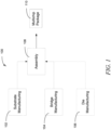
- FIG. 1 illustrates a general microelectronic process according to some embodiments.
- the process illustrated generally as 100, takes assemblies made from a substrate manufacturing process 102, a bridge manufacturing process 104 and assembles them as shown in 108 to produce a microelectronic package/device such as multichip package 110.
- Die manufacturing process 106 is illustrated in dashed form to indicate that the die can be assembled on the substrate and bridge in the same process 108 or in a separate process at a later time. Die manufacturing process 106 can be any process sufficient to produce desired dies that will be incorporated into the final product. No further description of die manufacturing 106 will be given as it is not important to the disclosure herein.
- Substrate manufacturing process 102 may comprise any process to produce a suitable package substrate that may be used, for example, in multi-chip packaging. Separate substrate manufacturing process 102 allows the process to be tuned effectively for the particular package substrate. In general, this means that the package substrates and process 102 can be tailored to only those aspects driven by the package substrate (and the bridge placement) and not those aspects driven by the bridge itself. In general, this allows using a less expensive process, a process that provides a higher yield, a higher volume, more relaxed geometries on conductors on and within the package substrate, a combination of all of these, or some other particular criteria or combination of criteria.
- package substrates are made from an organic polymer such as an epoxy. Package substrates may have a variety of materials such as silica, calcium oxide, magnesium oxide, etc., added to the organic polymer to achieve particular properties such as a desired glass transition temperature or other desired properties.
- Package substrates produced by substrate manufacturing process 102 may include various layers and geometries such as wires and connection points.
- substrates can be produced using design rules of about a 40 ⁇ m wire width and about a 40 ⁇ m wire spacing.
- build-up layers, if any, can be thicker than those used by bridge manufacturing process 104 to produce organic bridges.
- Bridge manufacturing process 104 may comprise a process to produce a high density interconnect bridge suitable for placement in the package substrate. An example process is discussed in conjunction with FIG. 4 below. Bridges may be made from an organic polymer such as an epoxy without its own substrate (e.g. with only a few build-up layers or a single build-up layer comprising routing and pad layers). In one embodiment organic bridges produced by bridge manufacturing process 104 are less than about 30 ⁇ m thick. In another embodiment, organic bridges produced by bridge manufacturing process 104 are about 15 ⁇ m thick.
- bridge manufacturing process 104 can use low cost, reusable glass carriers.
- the organic polymer used in bridge manufacturing process 104 to produce organic bridges may be the same as, or different from, the organic polymer of the substrate. Since both materials are organic, the organic bridges have better interfacial adhesion (compared, for example, to bridges made out of silicon). Since both materials are organic, cracking, chipping, delamination and other issues associated with use of dissimilar materials can be minimized.
- Bridge manufacturing process 104 may be designed to produce small, high density geometries in the bridge to carry high density IO interconnects.
- organic bridge manufacturing process 104 uses design rules of about 3 ⁇ m or less wire width and about 3 ⁇ m or less wire spacing.
- organic bridge manufacturing process 104 uses design rules of about 3 ⁇ m or less in wire width and spacing in some areas or layers and wider wire width and spacing in other areas or layers of the bridge (e.g., about 10 ⁇ m wire width and about 10 ⁇ m wire spacing).
- FIG. 2 illustrates a plan view of a microelectronic package according to some embodiments.
- the package 200 has package substrate 212 and an organic bridge 214 embedded in package substrate 212.
- Package substrate 212 may comprise an organic polymer such as an epoxy.
- Organic bridge 214 may also comprise an organic polymer such as an epoxy.
- the organic polymer of organic bridge 214 may be the same as, or different from, the organic polymer of package substrate 212.
- Organic bridge 214 comprises an interconnect structure 216 located at a location 220 and an interconnect structure 218 located at a location 222.
- Interconnect structure 216 and interconnect structure 218 may comprise a plurality of connection points, such as the connection point illustrated as 208.
- the various connection points within interconnect structure 216 and 218 are connected by conductive paths. In FIG. 2 , example conductive paths are illustrated by 210. Connections between the various connection points are appropriate to the die that will be interconnected by organic bridge 214.
- Locations 220 and 221, shown in dashed lines, indicate the locations where die interconnected by organic bridge 214 will be placed.
- Interconnect structures 216 & 218 on an organic bridge 214 are typically located toward an end of the organic bridge 214. Thus, locations 220 and 222 are typically toward the ends of organic bridge 214. However, the location of interconnect structures 216 & 218 are determined by the die that will be interconnected by the organic bridge 214.
- Microelectronic package 200 may comprise multiple organic bridges 214, each having multiple interconnect structures 216 & 218 in order to interconnect multiple die.
- additional organic bridges are illustrated by 202
- interconnect structures are illustrated by 204
- die placement locations are illustrated in dashed lines by 206.
- These organic bridges 202 may be similar to organic bridge 214.
- Interconnect structures 204 may be similar to interconnect structure 216 and/or interconnect structure 218.
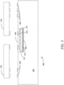
- FIG. 3 illustrates a cross sectional view of an organic bridge 202 placed within a substrate according to some embodiments.
- the assembly illustrated generally as 300, may comprise a substrate 302 and an organic bridge 304.
- Substrate 302 may be a package substrate 302, such as that manufactured by substrate manufacturing process 102 of FIG. 1 and may comprise an organic polymer such as an epoxy.
- Substrate 302 may comprise connection points 306 to connect a die, such as die 318 and 319 to substrate 302. Connection points 306 and associated conductive paths (not shown) may adhere to design rules appropriate for substrate 302. In one embodiment, the design rules of substrate 302 allow larger geometries (for e.g. connection points 306) than the design rules of embedded organic bridge 304. In one example, substrate 302 can be produced using design rules of about a 40 ⁇ m wire width and about a 40 ⁇ m wire spacing. Similarly, build-up layers, if any, can be thicker than those in organic bridge 304.
- Substrate 302 has a recess to receive organic bridge 304.
- the recess may only need to extend into the outermost layer or multiple outermost layers.
- Such a recess can be formed within substrate 302, for example, by using laser scribing.
- Organic bridge 304 may comprise an organic polymer such as an epoxy.
- the organic polymer of organic bridge 304 may be the same as, or different from, the organic polymer of substrate 302. For clarity, some of the various layers of organic bridge 304 are illustrated in various patterns so they can be distinguished from the surrounding items.
- Organic bridge 304 is placed into a recess of substrate 302 using an organic polymer to adhere organic bridge 304 into the recess.
- the organic polymer can be a dye bonding film, an epoxy, or any other type of organic polymer that sufficiently adheres organic bridge 304 to substrate 302.
- bonding organic bridge 304 to substrate 302 is illustrated by 308. Since substrate 302 and organic bridge 304 both comprise an organic polymer, layer 308 can adhere organic bridge 304 to substrate 302 in a way that minimizes problems arising from the interface of two dissimilar materials such as chipping, cracking and delamination.
- Organic bridge 304 is represented in FIG. 3 by layer 310, 312 and 314 and 316.
- Layer 310 represents a metal layer within organic bridge 304, which may be included as part of the bridge 304.
- Layer 314 represents a metal routing layer embedded within dielectric layer 312.
- Dielectric layer 312 comprises an organic polymer such as an epoxy and represents interleaved dielectric layers 312.
- Layer 316 represents a pad layer where, for example, interconnect structures 204 can be formed as part of organic bridge 304.
- the design rules for organic bridge 304 comprise about 3 ⁇ m or less wire width and about 3 ⁇ m or less wire spacing.
- the design rules for organic bridge 304 comprises about 3 ⁇ m or less in wire width and spacing in some areas or layers and wider wire width and spacing in other areas or layers of the bridge (e.g., about 10 ⁇ m wire width and about 10 ⁇ m wire spacing).
- organic bridge 304 have no substrate 302. Such embodiments may comprise routing and pad layers 314 & 316 and, possibly some additional metal layers all with interleaved dielectric layers 312 but without, for example, a substrate 302. Having no substrate 302 means that those embodiments of organic bridge 304 have no layer that has substantial silicon content. In such embodiments, any "substrate" layer would be made substantially of a metal or an organic polymer such as an epoxy.
- the organic polymer may include various additives such as silica, calcium oxide, magnesium oxide, or other additive to modify certain desired properties of the organic polymer.
- organic bridge 304 has no substrate 302 and is about 15 ⁇ m thick. In another embodiment organic bridge 304 has no substrate 302 and is less than about 20 ⁇ m thick. In yet another embodiment organic bridge 304 has no substrate 302 and is less than about 30 ⁇ m thick. Since organic bridge 304 has no substrate 302, it tends to conform to the contours of the recess into which it is placed. In such embodiments, the lack of a substrate 302 and the thinness of organic bridge 304 allows organic bridge 304 to be incorporated into a solder mask cavity on the surface layer of the of substrate 302 and ultra fine pitch dies can be directly connected by thermo-compression based bonding.
- FIG. 4 illustrates a process to create an organic bridge 304 according to some embodiments. Such a process can be used, for example, in bridge manufacturing process 104 of FIG. 1 .
- the process illustrated generally as 400 is a spin-on-glass (SoG) technique. SoG has the ability to provide finer trace and spacing than other processes, and thus is illustrated here. However, other processes may also be used.
- SoG spin-on-glass
- a carrier wafer of silicon or glass is obtained. Since the incoming carrier wafer will not form part of the final organic bridge 304, inexpensive, reusable carrier wafers can be used for the process.
- the dielectric layer 312 comprises an organic polymer such as an epoxy.
- seed layer deposition occurs, for example by sputtering. Dry file resist (DFR) and patterning of the seed layer also occurs.
- DFR Dry file resist
- plating occurs along with DFR stripping and application of the next dielectric layer 312 using SoG techniques.
- via formation occurs along with seed layer deposition using, for example, sputtering.
- DFR application and patterning also occurs.
- the resultant assembly is released from the carrier wafer and bridge singulation (e.g. separating the assembly into individual organic bridges 304) occurs.
- organic bridges 304 are only a few layers thick, perhaps only the routing layer 314 , pad layer 316, ground and reference layers for the signal layers, plus interleaved dielectric layers 312. In such a situation, this two layer organic bridge 304 will be about 15 ⁇ m thick. However, if desired, the process illustrated in 408 and/or 410 can be repeated as appropriate to achieve an organic bridge 304 of perhaps three or four layers having a thickness of about 20 ⁇ m to about 30 ⁇ m.
Landscapes
- Engineering & Computer Science (AREA)
- Microelectronics & Electronic Packaging (AREA)
- Internal Circuitry In Semiconductor Integrated Circuit Devices (AREA)
- Physics & Mathematics (AREA)
- Geometry (AREA)
- Production Of Multi-Layered Print Wiring Board (AREA)
- Wire Bonding (AREA)
- Combinations Of Printed Boards (AREA)
Abstract
Description
- This application claims the benefit of priority to
U.S. Patent Application Serial No. 13/722,203, filed on December 20, 2012 - Embodiments pertain to integrated circuit (IC) dies, multi-chip packages, and associated methods. More particularly, embodiments pertain to using an organic bridge in an organic package substrate to interconnect dies with a high density interconnect.
- In order to enhance performance, processing unit products are increasingly integrating multiple die within the processing unit package in a side-by-side or other multi-chip-module (MCM) format. In traditional MCM format, the chip die are interconnected via connections within the substrate. One way to increase the input-output (IO) capacity is to connect the die through embedded IO bridge die featuring a very high wiring density locally between die. Patterning dense metal features on a silicon substrate is the conventional fabrication approach. This enables very fine feature, size consistent backend metallization, and a great number of IO interconnections. However, there is a significant mismatch between the coefficient of thermal expansion (CTE) of an organic package and a silicon bridge, leading to delamination and cracking between multiple materials. With multiple process steps used in production of the MCM after the silicon bridge has been placed in the substrate, the manufacturing process itself can lead to cracking and delamination. Additionally, embedding an external bridge made out of silicon to increase the local IO makes the silicon bridge ultra-thin and embedding the silicon bridge within the substrate can be challenging.
-
-
FIG. 1 illustrates a general microelectronic process according to some embodiments; -
FIG. 2 illustrates a plan view of a microelectronic package according to some embodiments; -
FIG. 3 illustrates a cross sectional view of an organic bridge placed within a substrate according to some embodiments; and -
FIG. 4 illustrates a process to create an organic bridge according to some embodiments. - The following description and the drawings sufficiently illustrate specific embodiments to enable those skilled in the art to practice them. Other embodiments may incorporate structural, logical, electrical, process, and other changes. Portions and features of some embodiments may be included in, or substituted for, those of other embodiments. Embodiments set forth in the claims encompass all available equivalents of those claims.
-
FIG. 1 illustrates a general microelectronic process according to some embodiments. The process, illustrated generally as 100, takes assemblies made from asubstrate manufacturing process 102, abridge manufacturing process 104 and assembles them as shown in 108 to produce a microelectronic package/device such asmultichip package 110. - Die
manufacturing process 106 is illustrated in dashed form to indicate that the die can be assembled on the substrate and bridge in thesame process 108 or in a separate process at a later time. Diemanufacturing process 106 can be any process sufficient to produce desired dies that will be incorporated into the final product. No further description of diemanufacturing 106 will be given as it is not important to the disclosure herein. -
Substrate manufacturing process 102 may comprise any process to produce a suitable package substrate that may be used, for example, in multi-chip packaging. Separatesubstrate manufacturing process 102 allows the process to be tuned effectively for the particular package substrate. In general, this means that the package substrates andprocess 102 can be tailored to only those aspects driven by the package substrate (and the bridge placement) and not those aspects driven by the bridge itself. In general, this allows using a less expensive process, a process that provides a higher yield, a higher volume, more relaxed geometries on conductors on and within the package substrate, a combination of all of these, or some other particular criteria or combination of criteria. Typically package substrates are made from an organic polymer such as an epoxy. Package substrates may have a variety of materials such as silica, calcium oxide, magnesium oxide, etc., added to the organic polymer to achieve particular properties such as a desired glass transition temperature or other desired properties. - Package substrates produced by
substrate manufacturing process 102 may include various layers and geometries such as wires and connection points. In one example, substrates can be produced using design rules of about a 40µm wire width and about a 40µm wire spacing. Similarly, build-up layers, if any, can be thicker than those used bybridge manufacturing process 104 to produce organic bridges. -
Bridge manufacturing process 104 may comprise a process to produce a high density interconnect bridge suitable for placement in the package substrate. An example process is discussed in conjunction withFIG. 4 below. Bridges may be made from an organic polymer such as an epoxy without its own substrate (e.g. with only a few build-up layers or a single build-up layer comprising routing and pad layers). In one embodiment organic bridges produced bybridge manufacturing process 104 are less than about 30µm thick. In another embodiment, organic bridges produced bybridge manufacturing process 104 are about 15µm thick. - In embodiments of the bridge that have no substrate, when the bridge is placed on the package substrate as part of
assembly process 108, the bridge conforms to the contours of the layer in the package substrate beneath it. This helps minimize inter-material issues such as cracking, chipping or delamination. The thinness of the bridge makes it easier to satisfy any z-height requirements of the process and/or package. For embodiments manufactured without a substrate,bridge manufacturing process 104 can use low cost, reusable glass carriers. - The organic polymer used in
bridge manufacturing process 104 to produce organic bridges may be the same as, or different from, the organic polymer of the substrate. Since both materials are organic, the organic bridges have better interfacial adhesion (compared, for example, to bridges made out of silicon). Since both materials are organic, cracking, chipping, delamination and other issues associated with use of dissimilar materials can be minimized. -
Bridge manufacturing process 104 may be designed to produce small, high density geometries in the bridge to carry high density IO interconnects. In one embodiment, organicbridge manufacturing process 104 uses design rules of about 3µm or less wire width and about 3µm or less wire spacing. In another embodiment, organicbridge manufacturing process 104 uses design rules of about 3µm or less in wire width and spacing in some areas or layers and wider wire width and spacing in other areas or layers of the bridge (e.g., about 10µm wire width and about 10µm wire spacing). -
FIG. 2 illustrates a plan view of a microelectronic package according to some embodiments. Thepackage 200 haspackage substrate 212 and anorganic bridge 214 embedded inpackage substrate 212.Package substrate 212 may comprise an organic polymer such as an epoxy.Organic bridge 214 may also comprise an organic polymer such as an epoxy. The organic polymer oforganic bridge 214 may be the same as, or different from, the organic polymer ofpackage substrate 212. -
Organic bridge 214 comprises aninterconnect structure 216 located at alocation 220 and aninterconnect structure 218 located at alocation 222.Interconnect structure 216 andinterconnect structure 218 may comprise a plurality of connection points, such as the connection point illustrated as 208. The various connection points withininterconnect structure FIG. 2 , example conductive paths are illustrated by 210. Connections between the various connection points are appropriate to the die that will be interconnected byorganic bridge 214.Locations organic bridge 214 will be placed. -
Interconnect structures 216 & 218 on anorganic bridge 214 are typically located toward an end of theorganic bridge 214. Thus,locations organic bridge 214. However, the location ofinterconnect structures 216 & 218 are determined by the die that will be interconnected by theorganic bridge 214. -
Microelectronic package 200 may comprise multipleorganic bridges 214, each havingmultiple interconnect structures 216 & 218 in order to interconnect multiple die. InFIG. 2 , additional organic bridges are illustrated by 202, interconnect structures are illustrated by 204 and die placement locations are illustrated in dashed lines by 206. Theseorganic bridges 202 may be similar toorganic bridge 214.Interconnect structures 204 may be similar tointerconnect structure 216 and/orinterconnect structure 218. -
FIG. 3 illustrates a cross sectional view of anorganic bridge 202 placed within a substrate according to some embodiments. The assembly, illustrated generally as 300, may comprise asubstrate 302 and anorganic bridge 304.Substrate 302 may be apackage substrate 302, such as that manufactured bysubstrate manufacturing process 102 ofFIG. 1 and may comprise an organic polymer such as an epoxy. -
Substrate 302 may comprise connection points 306 to connect a die, such asdie substrate 302. Connection points 306 and associated conductive paths (not shown) may adhere to design rules appropriate forsubstrate 302. In one embodiment, the design rules ofsubstrate 302 allow larger geometries (for e.g. connection points 306) than the design rules of embeddedorganic bridge 304. In one example,substrate 302 can be produced using design rules of about a 40µm wire width and about a 40µm wire spacing. Similarly, build-up layers, if any, can be thicker than those inorganic bridge 304. -
Substrate 302 has a recess to receiveorganic bridge 304. Depending on the thickness of the dielectric and other layers ofsubstrate 302 and the thickness oforganic bridge 304, the recess may only need to extend into the outermost layer or multiple outermost layers. Such a recess can be formed withinsubstrate 302, for example, by using laser scribing. -
Organic bridge 304 may comprise an organic polymer such as an epoxy. The organic polymer oforganic bridge 304 may be the same as, or different from, the organic polymer ofsubstrate 302. For clarity, some of the various layers oforganic bridge 304 are illustrated in various patterns so they can be distinguished from the surrounding items. -
Organic bridge 304 is placed into a recess ofsubstrate 302 using an organic polymer to adhereorganic bridge 304 into the recess. The organic polymer can be a dye bonding film, an epoxy, or any other type of organic polymer that sufficiently adheresorganic bridge 304 tosubstrate 302. InFIG. 3 , bondingorganic bridge 304 tosubstrate 302 is illustrated by 308. Sincesubstrate 302 andorganic bridge 304 both comprise an organic polymer,layer 308 can adhereorganic bridge 304 tosubstrate 302 in a way that minimizes problems arising from the interface of two dissimilar materials such as chipping, cracking and delamination. -
Organic bridge 304 is represented inFIG. 3 bylayer Layer 310 represents a metal layer withinorganic bridge 304, which may be included as part of thebridge 304.Layer 314 represents a metal routing layer embedded withindielectric layer 312.Dielectric layer 312 comprises an organic polymer such as an epoxy and represents interleaved dielectric layers 312.Layer 316 represents a pad layer where, for example,interconnect structures 204 can be formed as part oforganic bridge 304. In one embodiment, the design rules fororganic bridge 304 comprise about 3µm or less wire width and about 3µm or less wire spacing. In another embodiment, the design rules fororganic bridge 304 comprises about 3µm or less in wire width and spacing in some areas or layers and wider wire width and spacing in other areas or layers of the bridge (e.g., about 10µm wire width and about 10µm wire spacing). - Some embodiments of
organic bridge 304 have nosubstrate 302. Such embodiments may comprise routing andpad layers 314 & 316 and, possibly some additional metal layers all with interleaveddielectric layers 312 but without, for example, asubstrate 302. Having nosubstrate 302 means that those embodiments oforganic bridge 304 have no layer that has substantial silicon content. In such embodiments, any "substrate" layer would be made substantially of a metal or an organic polymer such as an epoxy. The organic polymer may include various additives such as silica, calcium oxide, magnesium oxide, or other additive to modify certain desired properties of the organic polymer. - In one embodiment
organic bridge 304 has nosubstrate 302 and is about 15µm thick. In another embodimentorganic bridge 304 has nosubstrate 302 and is less than about 20µm thick. In yet another embodimentorganic bridge 304 has nosubstrate 302 and is less than about 30µm thick. Sinceorganic bridge 304 has nosubstrate 302, it tends to conform to the contours of the recess into which it is placed. In such embodiments, the lack of asubstrate 302 and the thinness oforganic bridge 304 allowsorganic bridge 304 to be incorporated into a solder mask cavity on the surface layer of the ofsubstrate 302 and ultra fine pitch dies can be directly connected by thermo-compression based bonding. -
FIG. 4 illustrates a process to create anorganic bridge 304 according to some embodiments. Such a process can be used, for example, inbridge manufacturing process 104 ofFIG. 1 . InFIG. 4 , the process illustrated generally as 400 is a spin-on-glass (SoG) technique. SoG has the ability to provide finer trace and spacing than other processes, and thus is illustrated here. However, other processes may also be used. - In 402 a carrier wafer of silicon or glass is obtained. Since the incoming carrier wafer will not form part of the final
organic bridge 304, inexpensive, reusable carrier wafers can be used for the process. - In 404 a release layer and the lower dielectric (SoG) layer is deposited. As previously described, the
dielectric layer 312 comprises an organic polymer such as an epoxy. - In 406, seed layer deposition occurs, for example by sputtering. Dry file resist (DFR) and patterning of the seed layer also occurs.
- In 408, plating occurs along with DFR stripping and application of the next
dielectric layer 312 using SoG techniques. - In 410 via formation occurs along with seed layer deposition using, for example, sputtering. DFR application and patterning also occurs.
- In 412 continuation of all metal layers occurs along with the final solder resist (SR) layer and patterning.
- In 414 the resultant assembly is released from the carrier wafer and bridge singulation (e.g. separating the assembly into individual organic bridges 304) occurs.
- In general,
organic bridges 304, such as those described in conjunction withFIGs. 1-3 , are only a few layers thick, perhaps only therouting layer 314 ,pad layer 316, ground and reference layers for the signal layers, plus interleaved dielectric layers 312. In such a situation, this two layerorganic bridge 304 will be about 15µm thick. However, if desired, the process illustrated in 408 and/or 410 can be repeated as appropriate to achieve anorganic bridge 304 of perhaps three or four layers having a thickness of about 20µm to about 30µm. - The above detailed description includes references to the accompanying drawings, which form a part of the detailed description. The drawings show, by way of illustration, specific embodiments in which the disclosure may be practiced. These embodiments are also referred to herein as "examples." Such examples may include elements in addition to those shown or described. However, the present inventors also contemplate examples in which only those elements shown or described are provided. Moreover, the present inventors also contemplate examples using any combination or permutation of those elements shown or described (or one or more aspects thereof), either with respect to a particular example (or one or more aspects thereof), or with respect to other examples (or one or more aspects thereof) shown or described herein.
- In this document, the terms "a" or "an" are used, as is common in patent documents, to include one or more than one, independent of any other instances or usages of "at least one" or "one or more." In this document, the term "or" is used to refer to a nonexclusive or, such that "A or B" includes "A but not B," "B but not A," and "A and B," unless otherwise indicated. In this document, the terms "including" and "in which" are used as the plain-English equivalents of the respective terms "comprising" and "wherein." Also, in the following claims, the terms "including" and "comprising" are open-ended, that is, a system, device, article, composition, formulation, or process that includes elements in addition to those listed after such a term in a claim are still deemed to fall within the scope of that claim. Moreover, in the following claims, the terms "first," "second," and "third," etc. are used merely as labels, and are not intended to impose numerical requirements on their objects.
- The above description is intended to be illustrative, and not restrictive. For example, the above-described examples (or one or more aspects thereof) may be used in combination with each other. Other embodiments may be used, such as by one of ordinary skill in the art upon reviewing the above description. The Abstract is provided to comply with 37 C.F.R. §1.72(b), to allow the reader to quickly ascertain the nature of the technical disclosure. It is submitted with the understanding that it will not be used to interpret or limit the scope or meaning of the claims. Also, in the above Detailed Description, various features may be grouped together to streamline the disclosure. This should not be interpreted as intending that an unclaimed disclosed feature is essential to any claim. Rather, inventive subject matter may lie in less than all features of a particular disclosed embodiment. Thus, the following claims are hereby incorporated into the Detailed Description, with each claim standing on its own as a separate embodiment, and it is contemplated that such embodiments may be combined with each other in various combinations or permutations. The scope of the inventive material should be determined with reference to the appended claims, along with the full scope of equivalents to which such claims are entitled.
Claims (15)
- A device comprising:a substrate;a first die electrically coupled to the substrate;a second die electrically coupled to the substrate; anda bridge in the substrate, the bridge including:wherein the first die is electrically coupled with the first metal pad of the bridge, and the second die is electrically coupled with the second metal pad of the bridge.a layer comprising a polymer;a first metal pad over the layer;a second metal pad over the layer; anda conductive path electrically coupling the first metal pad to the second metal pad;
- The device of claim 1, wherein the first metal pad is proximate a first end of the bridge and the second metal pad is proximate a second opposing end of the bridge.
- The device of one of the previous claims, further comprising:a third metal pad over the layer;a fourth metal pad over the layer; anda second conductive path electrically coupling the third metal pad to the fourth metal pad;wherein the first die is electrically coupled with the third metal pad and the second die is electrically coupled with the fourth metal pad.
- The device of one of the previous claims, wherein the layer comprises a first layer, the bridge further including a second layer on the first layer, the second layer comprising a dielectric.
- The device of claim 4, wherein the polymer of the first layer and the dielectric of the second layer are the same.
- The interconnect bridge of claim 4 or 5, wherein the first metal pad and the second metal pad are on the second layer, and at least a portion of the conductive path is on the first layer.
- The device of one of the previous claims, wherein the bridge does not include a layer of silicon.
- The device of one of the previous claims, wherein the polymer includes silica.
- The device of one of the previous claims, wherein the substrate includes a recess and the bridge is in the recess.
- A method of making an interconnect bridge, the interconnect bridge for embedding in a substrate to electrically connect a first die to a second die, the method comprising:providing a layer comprising an organic material;forming a first metal pad and a second metal pad over the layer, wherein the first metal pad and the second metal pad are for electrical coupling with the first die;forming a third metal pad and a fourth metal pad over the first layer, wherein the third metal pad and the fourth metal pad are for electrical coupling with the second die;forming a first conductive path electrically coupling the first metal pad to the third metal pad; andforming a second conductive path electrically coupling the second metal pad to the fourth metal pad.
- The method of making an interconnect bridge of claim 10, further comprising forming the interconnect bridge on a carrier.
- The method of making an interconnect bridge of claim 10 or 11, further comprising removing the interconnect bridge from the carrier.
- The method of making an interconnect bridge of claim 10, 11 or 12, wherein the carrier comprises silicon or glass.
- The method of making an interconnect bridge of claim 10, 11, 12 or 13, further comprising:locating the first metal pad and the second metal pad proximate a first end of the layer; andlocating the third metal pad and the fourth metal pad proximate a second end of the layer, the second end opposing the first end.
- The method of making an interconnect bridge of claim 10, 11, 12, 13 or 14, wherein the layer comprises a first layer, the method further comprising:
forming a second layer on the first layer, the second layer comprising a dielectric.
Applications Claiming Priority (4)
| Application Number | Priority Date | Filing Date | Title |
|---|---|---|---|
| US13/722,203 US9236366B2 (en) | 2012-12-20 | 2012-12-20 | High density organic bridge device and method |
| PCT/US2013/044440 WO2014098966A1 (en) | 2012-12-20 | 2013-06-06 | High density organic bridge device and method |
| EP17188479.4A EP3273476A1 (en) | 2012-12-20 | 2013-12-09 | High density organic bridge device and method |
| EP13196337.3A EP2747136B1 (en) | 2012-12-20 | 2013-12-09 | High density organic bridge device and method |
Related Parent Applications (2)
| Application Number | Title | Priority Date | Filing Date |
|---|---|---|---|
| EP17188479.4A Division EP3273476A1 (en) | 2012-12-20 | 2013-12-09 | High density organic bridge device and method |
| EP13196337.3A Division EP2747136B1 (en) | 2012-12-20 | 2013-12-09 | High density organic bridge device and method |
Publications (2)
| Publication Number | Publication Date |
|---|---|
| EP4440253A2 true EP4440253A2 (en) | 2024-10-02 |
| EP4440253A3 EP4440253A3 (en) | 2025-01-01 |
Family
ID=50973358
Family Applications (3)
| Application Number | Title | Priority Date | Filing Date |
|---|---|---|---|
| EP17188479.4A Ceased EP3273476A1 (en) | 2012-12-20 | 2013-12-09 | High density organic bridge device and method |
| EP13196337.3A Active EP2747136B1 (en) | 2012-12-20 | 2013-12-09 | High density organic bridge device and method |
| EP24186432.1A Pending EP4440253A3 (en) | 2012-12-20 | 2013-12-09 | High density organic bridge device and method |
Family Applications Before (2)
| Application Number | Title | Priority Date | Filing Date |
|---|---|---|---|
| EP17188479.4A Ceased EP3273476A1 (en) | 2012-12-20 | 2013-12-09 | High density organic bridge device and method |
| EP13196337.3A Active EP2747136B1 (en) | 2012-12-20 | 2013-12-09 | High density organic bridge device and method |
Country Status (9)
| Country | Link |
|---|---|
| US (6) | US9236366B2 (en) |
| EP (3) | EP3273476A1 (en) |
| JP (3) | JP2014140022A (en) |
| KR (2) | KR101593277B1 (en) |
| CN (1) | CN104037161B (en) |
| BR (1) | BR102013032406B1 (en) |
| SG (1) | SG2013093521A (en) |
| TW (1) | TWI556401B (en) |
| WO (1) | WO2014098966A1 (en) |
Families Citing this family (58)
| Publication number | Priority date | Publication date | Assignee | Title |
|---|---|---|---|---|
| US8227904B2 (en) * | 2009-06-24 | 2012-07-24 | Intel Corporation | Multi-chip package and method of providing die-to-die interconnects in same |
| US9136236B2 (en) | 2012-09-28 | 2015-09-15 | Intel Corporation | Localized high density substrate routing |
| US9190380B2 (en) | 2012-12-06 | 2015-11-17 | Intel Corporation | High density substrate routing in BBUL package |
| US9236366B2 (en) | 2012-12-20 | 2016-01-12 | Intel Corporation | High density organic bridge device and method |
| US8901748B2 (en) * | 2013-03-14 | 2014-12-02 | Intel Corporation | Direct external interconnect for embedded interconnect bridge package |
| US9147663B2 (en) | 2013-05-28 | 2015-09-29 | Intel Corporation | Bridge interconnection with layered interconnect structures |
| JP2014236188A (en) * | 2013-06-05 | 2014-12-15 | イビデン株式会社 | Wiring board and manufacturing method therefor |
| US9041205B2 (en) * | 2013-06-28 | 2015-05-26 | Intel Corporation | Reliable microstrip routing for electronics components |
| US9642259B2 (en) | 2013-10-30 | 2017-05-02 | Qualcomm Incorporated | Embedded bridge structure in a substrate |
| US20150364422A1 (en) * | 2014-06-13 | 2015-12-17 | Apple Inc. | Fan out wafer level package using silicon bridge |
| JP2016021496A (en) * | 2014-07-15 | 2016-02-04 | イビデン株式会社 | Wiring board and manufacturing method for the same |
| JP6665375B2 (en) | 2014-09-19 | 2020-03-13 | インテル・コーポレーション | Semiconductor package with embedded bridge-type interconnect |
| US9583426B2 (en) | 2014-11-05 | 2017-02-28 | Invensas Corporation | Multi-layer substrates suitable for interconnection between circuit modules |
| US9595496B2 (en) | 2014-11-07 | 2017-03-14 | Qualcomm Incorporated | Integrated device package comprising silicon bridge in an encapsulation layer |
| US9379090B1 (en) * | 2015-02-13 | 2016-06-28 | Qualcomm Incorporated | System, apparatus, and method for split die interconnection |
| US9443824B1 (en) | 2015-03-30 | 2016-09-13 | Qualcomm Incorporated | Cavity bridge connection for die split architecture |
| US10283492B2 (en) | 2015-06-23 | 2019-05-07 | Invensas Corporation | Laminated interposers and packages with embedded trace interconnects |
| US10477684B2 (en) * | 2015-09-25 | 2019-11-12 | Intel Corporation | Apparatus, system, and method including a bridge device for interfacing a package device with a substrate |
| US10177083B2 (en) | 2015-10-29 | 2019-01-08 | Intel Corporation | Alternative surfaces for conductive pad layers of silicon bridges for semiconductor packages |
| CN116110887A (en) * | 2015-12-11 | 2023-05-12 | 英特尔公司 | Microelectronic structure having multiple microelectronic devices connected by microelectronic bridges embedded in a microelectronic substrate |
| US9852994B2 (en) | 2015-12-14 | 2017-12-26 | Invensas Corporation | Embedded vialess bridges |
| WO2017111790A1 (en) | 2015-12-23 | 2017-06-29 | Manusharow Mathew J | Improving size and efficiency of dies |
| TWI701782B (en) * | 2016-01-27 | 2020-08-11 | 美商艾馬克科技公司 | Semiconductor package and fabricating method thereof |
| KR101966328B1 (en) * | 2016-03-29 | 2019-04-05 | 삼성전기주식회사 | Printed circuit board and manufacturing for the same |
| WO2017171738A1 (en) | 2016-03-30 | 2017-10-05 | Intel Corporation | Hybrid microelectronic substrates |
| US20170287838A1 (en) | 2016-04-02 | 2017-10-05 | Intel Corporation | Electrical interconnect bridge |
| WO2018004620A1 (en) * | 2016-06-30 | 2018-01-04 | Qian Zhiguo | Bridge die design for high bandwidth memory interface |
| EP3479398B1 (en) * | 2016-07-01 | 2025-02-19 | Intel Corporation | Molded embedded bridge for enhanced emib applications |
| KR102632563B1 (en) | 2016-08-05 | 2024-02-02 | 삼성전자주식회사 | Semiconductor Package |
| KR102595896B1 (en) * | 2016-08-08 | 2023-10-30 | 삼성전자 주식회사 | Printed Circuit Board, and semiconductor package having the same |
| EP3288076B1 (en) * | 2016-08-25 | 2021-06-23 | IMEC vzw | A semiconductor die package and method of producing the package |
| CN110024113B (en) * | 2016-11-30 | 2023-11-24 | 深圳修远电子科技有限公司 | Integrated circuit packaging structure and method |
| US11004824B2 (en) | 2016-12-22 | 2021-05-11 | Intel Corporation | Scalable embedded silicon bridge via pillars in lithographically defined vias, and methods of making same |
| US10943869B2 (en) * | 2017-06-09 | 2021-03-09 | Apple Inc. | High density interconnection using fanout interposer chiplet |
| US10622311B2 (en) * | 2017-08-10 | 2020-04-14 | International Business Machines Corporation | High-density interconnecting adhesive tape |
| EP3688800A4 (en) * | 2017-09-29 | 2021-05-19 | INTEL Corporation | HORIZONTAL STEP SHIFTING USING INTEGRATED BRIDGE CHIPS |
| US10483156B2 (en) * | 2017-11-29 | 2019-11-19 | International Business Machines Corporation | Non-embedded silicon bridge chip for multi-chip module |
| US10784202B2 (en) | 2017-12-01 | 2020-09-22 | International Business Machines Corporation | High-density chip-to-chip interconnection with silicon bridge |
| JP6912423B2 (en) * | 2018-01-04 | 2021-08-04 | 株式会社東芝 | Electronic device |
| US10475767B2 (en) | 2018-01-04 | 2019-11-12 | Kabushiki Kaisha Toshiba | Electronic device |
| US10580738B2 (en) * | 2018-03-20 | 2020-03-03 | International Business Machines Corporation | Direct bonded heterogeneous integration packaging structures |
| US11018124B2 (en) * | 2018-08-31 | 2021-05-25 | Intel Corporation | Embedded memory device and method for embedding memory device in a substrate |
| TWI662676B (en) | 2018-08-31 | 2019-06-11 | 欣興電子股份有限公司 | Circuit carrier with embedded substrate, manufacturing method thereof and chip package structure |
| TWI862101B (en) * | 2018-12-07 | 2024-11-11 | 新加坡商安靠科技新加坡控股私人有限公司 | Semiconductor package and fabricating method thereof |
| CN111372369B (en) | 2018-12-25 | 2023-07-07 | 奥特斯科技(重庆)有限公司 | Component carrier with component shielding and method for producing the same |
| US11756889B2 (en) * | 2019-08-07 | 2023-09-12 | Intel Corporation | Ultrathin bridge and multi-die ultrafine pitch patch architecture and method of making |
| US11569172B2 (en) * | 2019-08-08 | 2023-01-31 | Taiwan Semiconductor Manufacturing Co., Ltd. | Semiconductor devices and methods of manufacture |
| US10957650B2 (en) | 2019-08-21 | 2021-03-23 | International Business Machines Corporation | Bridge support structure |
| US11527462B2 (en) | 2019-12-13 | 2022-12-13 | International Business Machines Corporation | Circuit substrate with mixed pitch wiring |
| CN111769101B (en) * | 2020-07-09 | 2022-05-03 | 中国科学院微电子研究所 | Packaging structure and packaging method based on multiple transfer boards |
| US11532582B2 (en) * | 2020-08-25 | 2022-12-20 | Taiwan Semiconductor Manufacturing Co., Ltd. | Semiconductor device package and method of manufacture |
| US20230317619A1 (en) * | 2022-04-01 | 2023-10-05 | Intel Corporation | Microelectronic structure including die bonding film between embedded die and surface of substrate cavity, and method of making same |
| US12463178B2 (en) * | 2022-07-03 | 2025-11-04 | Taiwan Semiconductor Manufacturing Company, Ltd. | Semiconductor die assembly having a polygonal linking die |
| JPWO2024053103A1 (en) * | 2022-09-09 | 2024-03-14 | ||
| CN116053251A (en) * | 2022-12-13 | 2023-05-02 | 海光信息技术股份有限公司 | Packaging structure, chip, electronic device and chip packaging method |
| JPWO2024202681A1 (en) | 2023-03-30 | 2024-10-03 | ||
| CN116092948B (en) * | 2023-04-10 | 2025-02-28 | 北京华封集芯电子有限公司 | A method for manufacturing a chip and a chip |
| WO2024212974A1 (en) * | 2023-04-10 | 2024-10-17 | 北京华封集芯电子有限公司 | Interposer manufacturing method, chip manufacturing method, interposer, chip, and chip package |
Family Cites Families (60)
| Publication number | Priority date | Publication date | Assignee | Title |
|---|---|---|---|---|
| US3436604A (en) * | 1966-04-25 | 1969-04-01 | Texas Instruments Inc | Complex integrated circuit array and method for fabricating same |
| US3684818A (en) * | 1970-10-20 | 1972-08-15 | Sprague Electric Co | Multi-layer beam-lead wiring for semiconductor packages |
| JPS4989157A (en) * | 1972-12-29 | 1974-08-26 | ||
| US4054938A (en) * | 1974-05-13 | 1977-10-18 | American Microsystems, Inc. | Combined semiconductor device and printed circuit board assembly |
| US4055725A (en) * | 1974-05-13 | 1977-10-25 | Hollis Engineering, Inc. | Circuit board assembly |
| US4918811A (en) | 1986-09-26 | 1990-04-24 | General Electric Company | Multichip integrated circuit packaging method |
| US5093929A (en) * | 1987-05-29 | 1992-03-03 | Stolar, Inc. | Medium frequency mine communication system |
| US5192716A (en) * | 1989-01-25 | 1993-03-09 | Polylithics, Inc. | Method of making a extended integration semiconductor structure |
| US5019535A (en) * | 1989-03-28 | 1991-05-28 | General Electric Company | Die attachment method using nonconductive adhesive for use in high density interconnected assemblies |
| US5182632A (en) * | 1989-11-22 | 1993-01-26 | Tactical Fabs, Inc. | High density multichip package with interconnect structure and heatsink |
| JPH0377380U (en) | 1989-11-30 | 1991-08-02 | ||
| US5061657A (en) * | 1990-07-18 | 1991-10-29 | The United States Of America As Represented By The Secretary Of The Navy | Method of making integrated circuit to package electrical connections after encapsulation with an organic polymer |
| US5049978A (en) * | 1990-09-10 | 1991-09-17 | General Electric Company | Conductively enclosed hybrid integrated circuit assembly using a silicon substrate |
| US5768109A (en) * | 1991-06-26 | 1998-06-16 | Hughes Electronics | Multi-layer circuit board and semiconductor flip chip connection |
| US5130349A (en) * | 1991-11-07 | 1992-07-14 | Ppg Industries, Inc. | Intumescent flame retardant composition |
| US5198963A (en) * | 1991-11-21 | 1993-03-30 | Motorola, Inc. | Multiple integrated circuit module which simplifies handling and testing |
| US5469333A (en) | 1993-05-05 | 1995-11-21 | International Business Machines Corporation | Electronic package assembly with protective encapsulant material on opposing sides not having conductive leads |
| US5358604A (en) * | 1992-09-29 | 1994-10-25 | Microelectronics And Computer Technology Corp. | Method for producing conductive patterns |
| US5457878A (en) * | 1993-10-12 | 1995-10-17 | Lsi Logic Corporation | Method for mounting integrated circuit chips on a mini-board |
| JP2591499B2 (en) * | 1994-10-21 | 1997-03-19 | 日本電気株式会社 | Semiconductor device |
| JP3287181B2 (en) * | 1995-08-15 | 2002-05-27 | ソニー株式会社 | Connection structure of multilayer wiring |
| JP3583517B2 (en) * | 1995-09-20 | 2004-11-04 | 株式会社東芝 | Valve lock management device |
| US6750091B1 (en) | 1996-03-01 | 2004-06-15 | Micron Technology | Diode formation method |
| JP3437369B2 (en) * | 1996-03-19 | 2003-08-18 | 松下電器産業株式会社 | Chip carrier and semiconductor device using the same |
| US6314639B1 (en) * | 1998-02-23 | 2001-11-13 | Micron Technology, Inc. | Chip scale package with heat spreader and method of manufacture |
| US6317331B1 (en) | 1998-08-19 | 2001-11-13 | Kulicke & Soffa Holdings, Inc. | Wiring substrate with thermal insert |
| JP2000091273A (en) * | 1998-09-11 | 2000-03-31 | Sony Corp | Semiconductor package manufacturing method and structure |
| US6111756A (en) * | 1998-09-11 | 2000-08-29 | Fujitsu Limited | Universal multichip interconnect systems |
| US6690845B1 (en) * | 1998-10-09 | 2004-02-10 | Fujitsu Limited | Three-dimensional opto-electronic modules with electrical and optical interconnections and methods for making |
| KR100470386B1 (en) * | 1998-12-26 | 2005-05-19 | 주식회사 하이닉스반도체 | Multi-chip Package |
| SG93192A1 (en) * | 1999-01-28 | 2002-12-17 | United Microelectronics Corp | Face-to-face multi chip package |
| JP2001223306A (en) | 2000-02-14 | 2001-08-17 | Casio Micronics Co Ltd | Semiconductor device and method of manufacturing the same |
| JP2002084108A (en) | 2000-07-05 | 2002-03-22 | Matsushita Electric Ind Co Ltd | Transmission line chip, method of manufacturing the same, and multi-chip module |
| WO2002017392A2 (en) | 2000-08-24 | 2002-02-28 | Polymer Flip Chip Corporation | Polymer redistribution of flip chip bond pads |
| US6927471B2 (en) * | 2001-09-07 | 2005-08-09 | Peter C. Salmon | Electronic system modules and method of fabrication |
| US6627978B2 (en) | 2001-09-28 | 2003-09-30 | Intel Corporation | Chip package enabling increased input/output density |
| JP4380130B2 (en) * | 2002-09-13 | 2009-12-09 | ソニー株式会社 | Semiconductor device |
| US7035113B2 (en) | 2003-01-30 | 2006-04-25 | Endicott Interconnect Technologies, Inc. | Multi-chip electronic package having laminate carrier and method of making same |
| US7459781B2 (en) * | 2003-12-03 | 2008-12-02 | Wen-Kun Yang | Fan out type wafer level package structure and method of the same |
| US7799699B2 (en) * | 2004-06-04 | 2010-09-21 | The Board Of Trustees Of The University Of Illinois | Printable semiconductor structures and related methods of making and assembling |
| JP4581768B2 (en) * | 2005-03-16 | 2010-11-17 | ソニー株式会社 | Manufacturing method of semiconductor device |
| US7671449B2 (en) * | 2005-05-04 | 2010-03-02 | Sun Microsystems, Inc. | Structures and methods for an application of a flexible bridge |
| US7294552B2 (en) | 2005-08-29 | 2007-11-13 | Delphi Technologies, Inc. | Electrical contact for a MEMS device and method of making |
| JP4989157B2 (en) | 2006-08-31 | 2012-08-01 | セイコーインスツル株式会社 | Electric double layer capacitor |
| JP5296690B2 (en) * | 2007-01-11 | 2013-09-25 | パナソニック株式会社 | light source |
| KR100888195B1 (en) | 2007-08-06 | 2009-03-12 | 한국과학기술원 | Organic substrate manufacturing method with active element |
| US8102663B2 (en) * | 2007-09-28 | 2012-01-24 | Oracle America, Inc. | Proximity communication package for processor, cache and memory |
| JP2009231635A (en) * | 2008-03-24 | 2009-10-08 | Shinko Electric Ind Co Ltd | Wiring board and its manufacturing method, semiconductor device, and its manufacturing method |
| US8064224B2 (en) * | 2008-03-31 | 2011-11-22 | Intel Corporation | Microelectronic package containing silicon patches for high density interconnects, and method of manufacturing same |
| JP2009290144A (en) * | 2008-05-30 | 2009-12-10 | Toshiba Corp | Electronics, printed circuit board, and method for producing printed circuit board |
| US9082806B2 (en) | 2008-12-12 | 2015-07-14 | Stats Chippac, Ltd. | Semiconductor device and method of forming a vertical interconnect structure for 3-D FO-WLCSP |
| US8227904B2 (en) * | 2009-06-24 | 2012-07-24 | Intel Corporation | Multi-chip package and method of providing die-to-die interconnects in same |
| JP2011051584A (en) | 2009-08-07 | 2011-03-17 | Equos Research Co Ltd | Vehicle |
| US8212354B2 (en) * | 2009-12-17 | 2012-07-03 | Oracle America, Inc. | Active plastic bridge chips |
| US8274149B2 (en) * | 2010-03-29 | 2012-09-25 | Advanced Semiconductor Engineering, Inc. | Semiconductor device package having a buffer structure and method of fabricating the same |
| US8492197B2 (en) * | 2010-08-17 | 2013-07-23 | Stats Chippac, Ltd. | Semiconductor device and method of forming vertically offset conductive pillars over first substrate aligned to vertically offset BOT interconnect sites formed over second substrate |
| US9406587B2 (en) | 2012-06-26 | 2016-08-02 | Intel Corporation | Substrate conductor structure and method |
| US9236366B2 (en) | 2012-12-20 | 2016-01-12 | Intel Corporation | High density organic bridge device and method |
| US8866308B2 (en) * | 2012-12-20 | 2014-10-21 | Intel Corporation | High density interconnect device and method |
| US11327259B2 (en) * | 2017-12-07 | 2022-05-10 | Intel Corporation | Integrated circuit package with electro-optical interconnect circuitry |
-
2012
- 2012-12-20 US US13/722,203 patent/US9236366B2/en active Active
-
2013
- 2013-06-06 WO PCT/US2013/044440 patent/WO2014098966A1/en not_active Ceased
- 2013-12-06 JP JP2013252669A patent/JP2014140022A/en active Pending
- 2013-12-09 EP EP17188479.4A patent/EP3273476A1/en not_active Ceased
- 2013-12-09 EP EP13196337.3A patent/EP2747136B1/en active Active
- 2013-12-09 EP EP24186432.1A patent/EP4440253A3/en active Pending
- 2013-12-10 TW TW102145384A patent/TWI556401B/en active
- 2013-12-17 BR BR102013032406-0A patent/BR102013032406B1/en active IP Right Grant
- 2013-12-17 KR KR1020130157445A patent/KR101593277B1/en active Active
- 2013-12-17 SG SG2013093521A patent/SG2013093521A/en unknown
- 2013-12-20 CN CN201310757213.4A patent/CN104037161B/en active Active
-
2015
- 2015-12-10 JP JP2015241109A patent/JP6572495B2/en active Active
-
2016
- 2016-01-11 US US14/992,535 patent/US9548264B2/en active Active
- 2016-02-01 KR KR1020160012342A patent/KR101706997B1/en active Active
- 2016-11-14 US US15/350,393 patent/US10103105B2/en active Active
-
2018
- 2018-04-02 JP JP2018070970A patent/JP6677380B2/en active Active
- 2018-09-19 US US16/135,695 patent/US10672713B2/en active Active
-
2020
- 2020-06-01 US US16/889,190 patent/US12002762B2/en active Active
-
2024
- 2024-05-30 US US18/678,813 patent/US20240321762A1/en active Pending
Also Published As
| Publication number | Publication date |
|---|---|
| KR20140080427A (en) | 2014-06-30 |
| BR102013032406A2 (en) | 2014-08-26 |
| EP2747136B1 (en) | 2019-11-20 |
| KR101593277B1 (en) | 2016-02-11 |
| US9236366B2 (en) | 2016-01-12 |
| SG2013093521A (en) | 2014-07-30 |
| US20240321762A1 (en) | 2024-09-26 |
| US20190019755A1 (en) | 2019-01-17 |
| JP2016105484A (en) | 2016-06-09 |
| CN104037161A (en) | 2014-09-10 |
| CN104037161B (en) | 2017-03-01 |
| US9548264B2 (en) | 2017-01-17 |
| JP6677380B2 (en) | 2020-04-08 |
| EP4440253A3 (en) | 2025-01-01 |
| US20160133552A1 (en) | 2016-05-12 |
| TW201442201A (en) | 2014-11-01 |
| US10103105B2 (en) | 2018-10-16 |
| EP2747136A1 (en) | 2014-06-25 |
| JP6572495B2 (en) | 2019-09-11 |
| WO2014098966A1 (en) | 2014-06-26 |
| KR101706997B1 (en) | 2017-02-15 |
| TWI556401B (en) | 2016-11-01 |
| US10672713B2 (en) | 2020-06-02 |
| JP2018129528A (en) | 2018-08-16 |
| US12002762B2 (en) | 2024-06-04 |
| BR102013032406B1 (en) | 2021-05-25 |
| US20200294924A1 (en) | 2020-09-17 |
| KR20160025536A (en) | 2016-03-08 |
| US20140174807A1 (en) | 2014-06-26 |
| US20170125349A1 (en) | 2017-05-04 |
| JP2014140022A (en) | 2014-07-31 |
| EP3273476A1 (en) | 2018-01-24 |
Similar Documents
| Publication | Publication Date | Title |
|---|---|---|
| US20240321762A1 (en) | High density organic bridge device and method | |
| US9837372B1 (en) | Wafer-level die to package and die to die interconnects suspended over integrated heat sinks | |
| KR20250044724A (en) | High-performance hybrid bonding interconnect system | |
| US12469776B2 (en) | Semiconductor assembly comprising a 3D block and method of making the same | |
| KR20170136934A (en) | Semiconductor package including heat spreader and methods for manufacturing the same | |
| CN109037188A (en) | Semiconductor device package | |
| CN112908872A (en) | Method for producing an electronic chip | |
| US20260114329A1 (en) | Perpendicular semiconductor device assemblies and associated methods | |
| JPH07312374A (en) | Integrated circuit system and manufacturing method thereof | |
| CN109427729B (en) | Semiconductor device package and method of manufacturing the same | |
| US11735529B2 (en) | Side pad anchored by next adjacent via | |
| CN117080172A (en) | Semiconductor device and method of forming release structure for preformed substrate |
Legal Events
| Date | Code | Title | Description |
|---|---|---|---|
| PUAI | Public reference made under article 153(3) epc to a published international application that has entered the european phase |
Free format text: ORIGINAL CODE: 0009012 |
|
| STAA | Information on the status of an ep patent application or granted ep patent |
Free format text: STATUS: THE APPLICATION HAS BEEN PUBLISHED |
|
| AC | Divisional application: reference to earlier application |
Ref document number: 2747136 Country of ref document: EP Kind code of ref document: P Ref document number: 3273476 Country of ref document: EP Kind code of ref document: P |
|
| AK | Designated contracting states |
Kind code of ref document: A2 Designated state(s): AL AT BE BG CH CY CZ DE DK EE ES FI FR GB GR HR HU IE IS IT LI LT LU LV MC MK MT NL NO PL PT RO RS SE SI SK SM TR |
|
| REG | Reference to a national code |
Ref country code: DE Ref legal event code: R079 Free format text: PREVIOUS MAIN CLASS: H05K0003460000 Ipc: H01L0025065000 |
|
| PUAL | Search report despatched |
Free format text: ORIGINAL CODE: 0009013 |
|
| AK | Designated contracting states |
Kind code of ref document: A3 Designated state(s): AL AT BE BG CH CY CZ DE DK EE ES FI FR GB GR HR HU IE IS IT LI LT LU LV MC MK MT NL NO PL PT RO RS SE SI SK SM TR |
|
| RIC1 | Information provided on ipc code assigned before grant |
Ipc: H05K 1/03 20060101ALN20241122BHEP Ipc: H05K 3/46 20060101ALN20241122BHEP Ipc: H05K 3/34 20060101ALN20241122BHEP Ipc: H05K 1/18 20060101ALN20241122BHEP Ipc: H01L 21/48 20060101ALN20241122BHEP Ipc: H05K 1/14 20060101ALI20241122BHEP Ipc: H01L 23/14 20060101ALI20241122BHEP Ipc: H01L 23/13 20060101ALI20241122BHEP Ipc: H01L 21/683 20060101ALI20241122BHEP Ipc: H01L 23/538 20060101ALI20241122BHEP Ipc: H01L 23/482 20060101ALI20241122BHEP Ipc: H01L 25/065 20230101AFI20241122BHEP |
|
| STAA | Information on the status of an ep patent application or granted ep patent |
Free format text: STATUS: REQUEST FOR EXAMINATION WAS MADE |
|
| 17P | Request for examination filed |
Effective date: 20250701 |
|
| STAA | Information on the status of an ep patent application or granted ep patent |
Free format text: STATUS: EXAMINATION IS IN PROGRESS |
|
| 17Q | First examination report despatched |
Effective date: 20260316 |