EP4439984A1 - Auf nichtstandard-bussteuerung basierende programmierbare logikvorrichtungsarchitektur zur verbindung mehrerer bussteuerungen und erhöhter anzahl von pld-modulen - Google Patents
Auf nichtstandard-bussteuerung basierende programmierbare logikvorrichtungsarchitektur zur verbindung mehrerer bussteuerungen und erhöhter anzahl von pld-modulen Download PDFInfo
- Publication number
- EP4439984A1 EP4439984A1 EP24165837.6A EP24165837A EP4439984A1 EP 4439984 A1 EP4439984 A1 EP 4439984A1 EP 24165837 A EP24165837 A EP 24165837A EP 4439984 A1 EP4439984 A1 EP 4439984A1
- Authority
- EP
- European Patent Office
- Prior art keywords
- data transfer
- transfer layer
- bus controller
- read
- write
- Prior art date
- Legal status (The legal status is an assumption and is not a legal conclusion. Google has not performed a legal analysis and makes no representation as to the accuracy of the status listed.)
- Pending
Links
Images


Classifications
-
- H—ELECTRICITY
- H03—ELECTRONIC CIRCUITRY
- H03K—PULSE TECHNIQUE
- H03K19/00—Logic circuits, i.e. having at least two inputs acting on one output; Inverting circuits
- H03K19/02—Logic circuits, i.e. having at least two inputs acting on one output; Inverting circuits using specified components
- H03K19/173—Logic circuits, i.e. having at least two inputs acting on one output; Inverting circuits using specified components using elementary logic circuits as components
- H03K19/177—Logic circuits, i.e. having at least two inputs acting on one output; Inverting circuits using specified components using elementary logic circuits as components arranged in matrix form
- H03K19/17736—Structural details of routing resources
-
- G—PHYSICS
- G05—CONTROLLING; REGULATING
- G05B—CONTROL OR REGULATING SYSTEMS IN GENERAL; FUNCTIONAL ELEMENTS OF SUCH SYSTEMS; MONITORING OR TESTING ARRANGEMENTS FOR SUCH SYSTEMS OR ELEMENTS
- G05B19/00—Program-control systems
- G05B19/02—Program-control systems electric
- G05B19/04—Program control other than numerical control, i.e. in sequence controllers or logic controllers
- G05B19/05—Programmable logic controllers, e.g. simulating logic interconnections of signals according to ladder diagrams or function charts
- G05B19/052—Linking several PLC's
Definitions
- the present disclosure relates to electrical systems and, in particular, to an electrical system having programmable logic devices (PLDs) with a non-standard bus controller-based PLD architecture.
- PLDs programmable logic devices
- a bus controller-based PLD device can have a bus as well as programmable logic device (PLD) modules attached to the bus and a bus controller.
- the bus controller may have bus control logic, interface logic, input multiplexing logic and memory pages. Together, these features of the bus controller allow for management of multiple functionalities of the PLD modules.
- a bus controller-based programmable logic device (PLD) architecture includes a dual-port unit interposed between bus controllers.
- the dual port unit includes first and second data transfer layers.
- the first data transfer layer includes write and read areas for data transfer between the first and second bus controllers, respectively. A write to the read area is prevented during a read by the second bus controller.
- the second data transfer layer includes read and write areas for data transfer between the first and second bus controllers, respectively. A write to the read area is prevented during a read by the first bus controller.
- the bus controller-based PLD architecture further includes thirty-one or more PLD modules and a command sequence execution by the first and second bus controllers is triggered by one of the PLD modules.
- data is transferred along the first and second data transfer layers simultaneously.
- the first data transfer layer includes a data transfer control unit configured to prevent the write to the read area of the first data transfer layer during the read by the second bus controller and the second data transfer layer includes a data transfer control unit configured to prevent the write to the read area of the second data transfer layer during the read by the first bus controller.
- the data transfer control unit of the first data transfer layer is further configured to write data, which is prevented from being written to the read area of the first data transfer layer during the read by the second bus controller, to the write area of the first data transfer layer during the read by the second bus controller and the data transfer control unit of the second data transfer layer is further configured to write data, which is prevented from being written to the read area of the second data transfer layer during the read by the first bus controller, to the write area of the second data transfer layer during the read by the first bus controller.
- the data transfer control unit of the first data transfer layer is further configured to mirror data in one system clock, which is written to the write area of the first data transfer layer, to the read area of the first data transfer layer following the read by the second bus controller and the data transfer control unit of the second data transfer layer is further configured to mirror data in one system clock, which is written to the write area of the second data transfer layer, to the read area of the second data transfer layer following the read by the first bus controller.
- a bus controller-based programmable logic device (PLD) architecture includes PLD modules, first and second bus controllers each responsive to a trigger by one of the PLD modules and a dual-port unit interposed between the first and second bus controllers.
- the dual port unit includes first and second data transfer layers.
- the first data transfer layer includes write and read areas for data transfer between the first and second bus controllers, respectively. A write to the read area is prevented during a read by the second bus controller.
- the second data transfer layer includes read and write areas for data transfer between the first and second bus controllers, respectively. A write to the read area is prevented during a read by the first bus controller.
- the PLD modules include up to thirty-one or more PLD modules.
- each of the first and second bus controllers includes control logic, interface logic, input multiplexing logic and memory.
- data is transferred along the first and second data transfer layers simultaneously.
- the first data transfer layer includes a data transfer control unit configured to prevent the write to the read area of the first data transfer layer during the read by the second bus controller and the second data transfer layer includes a data transfer control unit configured to prevent the write to the read area of the second data transfer layer during the read by the first bus controller.
- the data transfer control unit of the first data transfer layer is further configured to write data, which is prevented from being written to the read area of the first data transfer layer during the read by the second bus controller, to the write area of the first data transfer layer during the read by the second bus controller and the data transfer control unit of the second data transfer layer is further configured to write data, which is prevented from being written to the read area of the second data transfer layer during the read by the first bus controller, to the write area of the second data transfer layer during the read by the first bus controller.
- the data transfer control unit of the first data transfer layer is further configured to mirror data in one system clock, which is written to the write area of the first data transfer layer, to the read area of the first data transfer layer following the read by the second bus controller and the data transfer control unit of the second data transfer layer is further configured to mirror data in one system clock, which is written to the write area of the second data transfer layer, to the read area of the second data transfer layer following the read by the first bus controller.
- a method of operating a bus controller-based programmable logic device (PLD) architecture including PLD modules and first and second bus controllers includes receiving a trigger from one of the PLD modules at one of the first and second bus controllers and executing a command sequence by the one of the first and second bus controllers by exchanging data between the first and second bus controllers across a dual-port unit comprising first and second data transfer layers.
- PLD programmable logic device
- the exchanging of the data includes reading, from a read area of the first data transfer layer, by the second bus controller and preventing a write to the read area during the reading by the second bus controller and reading, from a read area of the second data transfer layer, by the first bus controller and preventing a write to the read area during the reading by the first bus controller.
- the PLD modules include up to thirty-one or more PLD modules.
- each of the first and second bus controllers includes control logic, interface logic, input multiplexing logic and memory.
- data is transferred along the first and second data transfer layers simultaneously.
- the preventing of the write to the read area of the first data transfer layer during the reading by the second bus controller is executed by a data transfer control unit of the first data transfer layer and the preventing of the write to the read area of the second data transfer layer during the reading by the first bus controller is executed by a data transfer control unit of the second data transfer layer.
- the method further includes writing data, which is prevented from being written to the read area of the first data transfer layer during the reading by the second bus controller, to the write area of the first data transfer layer by the data transfer control unit of the first data transfer layer during the reading by the second bus controller and writing data, which is prevented from being written to the read area of the second data transfer layer during the reading by the first bus controller, to the write area of the second data transfer layer by the data transfer control unit of the second data transfer layer during the reading by the first bus controller.
- the method further includes mirroring data in one system clock, which is written to the write area of the first data transfer layer, to the read area of the first data transfer layer by the data transfer control unit of the first data transfer layer following the reading by the second bus controller and mirroring data in one system clock, which is written to the write area of the second data transfer layer, to the read area of the second data transfer layer by the data transfer control unit of the second data transfer layer following the reading by the first bus controller
- a conventional bus controller-based PLD device can be characterized in that a bus controller manages multiple functionalities of the PLD modules, the conventional bus controller-based PLD device cannot provide a solution for more than a certain number of PLD modules (i.e., 31 PLD modules). Also, the conventional bus controller-based PLD cannot handle cases in which an application requires synchronization of data and control for multiple motor controllers, multiple digital bus controllers or one motor controller with a digital bus controller. In these or other cases, a bus controller command sequence can be triggered by only one system event whereupon the bus controller command sequence will run sequentially following the event. One bus controller therefore cannot manage two or more than two system triggers.
- bus controller-based PLD architecture is provided with multiple bus controllers and a mechanism by which the multiple bus controllers communicate. That is, a dual port-based architecture is provided which connects two (or more) bus controllers and transfers data according to the following: (1) to provide a mechanism for data exchange between two independently operating bus controllers with associated paged memories, (2) to define one custom memory page with separate write and read areas for each of the bus controllers, (3) to provide a configurable trigger location characterized in that a write to this location by a bus controller triggers copying of the updated (WS- write status set) write data to the read area of the other bus controller page, (4) to provide a fixed write disable (locks) register (location 0 of write area) so that a write to this location by a bus controller protects read data from being overwritten by the copy operation of the other bus controller during a read operation and (5) to support configurable depth (configurable for each data transfer pair) and page number.
- a dual port-based architecture which connects two (or more) bus controllers and transfers data
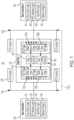
- a bus controller-based PLD architecture 101 includes busses 110 1 and 110 2 , PLD modules 120 coupled to the busses 110 1 and 110 2 (i.e., up to thirty-one or more PLD modules 120 can be coupled to the busses 110 1 and 110 2 ), a first bus controller 130, a second bus controller 140 and a dual-port unit 150.
- the busses 110 1 and 110 2 can be separate from one another or tied together by a further bus 110 3 . In the case of the busses 110 1 and 110 2 being separate from one another, there can be one bus controller per bus in the bus controller-based PLD architecture 101.
- the first bus controller 130 is coupled to the bus 110i and is configured to execute a command sequence 201 (see FIG.
- the second bus controller 140 is coupled to the bus 110 2 and is configured to execute another command sequence 202 (see FIG. 2 ) responsive to a trigger by another one of the PLD modules 120.
- the dual-port unit 150 is communicatively interposed between the first bus controller 130 and the second bus controller 140.
- the first bus controller 130 includes control logic 131, interface logic 132, input multiplexing logic 133 and memory 134.
- the second bus controller 140 includes control logic 141, interface logic 142, input multiplexing logic 143 and memory 144.
- the dual-port unit 150 includes a first data transfer layer 151 and a second data transfer layer 152 such that data is transferred between the first and second bus controllers 130 and 140 along the first and second data transfer layers 151 and 152 simultaneously.
- the first data transfer layer 151 includes a write area 1511 and a read area 1512 for data transfer between the first and second bus controllers 130 and 140, respectively, with a write to the read area 1512 being prevented during a read of the read area 1512 by the second bus controller 140.
- the second data transfer layer 152 includes a read area 1521 and a write area 1522 for command sequence execution by the first and second bus controllers 130 and 140, respectively, with a write to the read area 1521 being prevented during a read of the read area 1521 by the first bus controller 130.
- the first data transfer layer 151 further includes a data transfer control unit 161, which is interposed between the write area 1511 and the read area 1512, and which is configured to prevent the write to the read area 1512 during the read by the second bus controller 140.
- the data transfer control unit 161 of the first data transfer layer 151 is further configured to write data, which is prevented from being written to the read area 1512 of the first data transfer layer 151 during the read by the second bus controller 140, to the write area 1511 of the first data transfer layer 151 during the read by the second bus controller 140.
- the data transfer control unit 161 of the first data transfer layer 151 is also further configured to mirror data in one system clock, which is written to the write area 1511 of the first data transfer layer 151, to the read area 1512 of the first data transfer layer 151 following the read by the second bus controller 140.
- the second data transfer layer 152 further includes a data transfer control unit 162, which is interposed between the read area 1521 and the write area 1522, and which is configured to prevent the write to the read area 1521 during the read by the first bus controller 130.
- the data transfer control unit 162 of the second data transfer layer 152 is further configured to write data, which is prevented from being written to the read area 1521 of the second data transfer layer 152 during the read by the first bus controller 130, to the write area 1522 of the second data transfer layer 152 during the read by the first bus controller 130.
- the data transfer control unit 162 of the second data transfer layer 152 is also further configured to mirror data in one system clock, which is written to the write area 1522 of the second data transfer layer 152, to the read area 1521 of the second data transfer layer 152 following the read by the first bus controller 130.
- the command sequences executed by each of the first and second bus controllers 130 and 140 across the dual-port unit 150 can be executed simultaneously or substantially simultaneously. This can be done, for example, using multiple first data transfer layers 151 and multiple second data transfer layers 152 or by segregating lines of the write area 1511 and the read area 1512 of the first data transfer layer 151 and of the read area 1521 and the write area 1522 in the second data transfer layer 152.
- a method 300 of operating a bus controller-based PLD architecture in which PLD modules and first and second bus controllers are coupled to busses is provided (as described above). As shown in FIG. 3 , the method includes receiving a trigger from one of the PLD modules at one of the first and second bus controllers (block 301) and executing a command sequence by the one of the first and second bus controllers by exchanging data between the first and second bus controllers across a dual-port unit comprising first and second data transfer layers (block 302).
- the exchanging of the data of block 302 includes reading, from a read area of the first data transfer layer, by the second bus controller (block 3021) and preventing, by a data transfer control unit of the first data transfer layer, a write to the read area during the reading by the second bus controller (block 3022) and reading, from a read area of the second data transfer layer, by the first bus controller (block 3023) and preventing, by a data transfer control unit of the second data transfer layer, a write to the read area during the reading by the first bus controller (block 3024).
- the method 300 can further include writing data, which is prevented from being written to the read area of the first data transfer layer during the reading by the second bus controller, to the write area of the first data transfer layer by the data transfer control unit of the first data transfer layer during the reading by the second bus controller (block 3025) and writing data, which is prevented from being written to the read area of the second data transfer layer during the reading by the first bus controller, to the write area of the second data transfer layer by the data transfer control unit of the second data transfer layer during the reading by the first bus controller (block 3026).
- the method 300 can also include mirroring data in one system clock, which is written to the write area of the first data transfer layer, to the read area of the first data transfer layer by the data transfer control unit of the first data transfer layer following the reading by the second bus controller (block 3027) and mirroring data in one system clock, which is written to the write area of the second data transfer layer, to the read area of the second data transfer layer by the data transfer control unit of the second data transfer layer following the reading by the first bus controller (block 3028).
- bus controller-based PLD architecture that can be developed without modification with bus controllers to support more than a certain number of PLD modules (i.e., up to or more than 31 PLD modules) with a required level of synchronization of data and control flow.
Landscapes
- Physics & Mathematics (AREA)
- Engineering & Computer Science (AREA)
- Mathematical Physics (AREA)
- General Physics & Mathematics (AREA)
- Automation & Control Theory (AREA)
- Computer Networks & Wireless Communication (AREA)
- Computer Hardware Design (AREA)
- Computing Systems (AREA)
- General Engineering & Computer Science (AREA)
- Bus Control (AREA)
- Programmable Controllers (AREA)
- Logic Circuits (AREA)
Applications Claiming Priority (1)
| Application Number | Priority Date | Filing Date | Title |
|---|---|---|---|
| IN202311020307 | 2023-03-23 |
Publications (1)
| Publication Number | Publication Date |
|---|---|
| EP4439984A1 true EP4439984A1 (de) | 2024-10-02 |
Family
ID=90468554
Family Applications (1)
| Application Number | Title | Priority Date | Filing Date |
|---|---|---|---|
| EP24165837.6A Pending EP4439984A1 (de) | 2023-03-23 | 2024-03-25 | Auf nichtstandard-bussteuerung basierende programmierbare logikvorrichtungsarchitektur zur verbindung mehrerer bussteuerungen und erhöhter anzahl von pld-modulen |
Country Status (3)
| Country | Link |
|---|---|
| US (1) | US12602023B2 (de) |
| EP (1) | EP4439984A1 (de) |
| CA (1) | CA3232677A1 (de) |
Citations (2)
| Publication number | Priority date | Publication date | Assignee | Title |
|---|---|---|---|---|
| US5771227A (en) * | 1995-03-08 | 1998-06-23 | International Business Machines Corporation | Method and system for routing massages in a multi-node data communication network |
| JP2008228207A (ja) * | 2007-03-15 | 2008-09-25 | Ricoh Co Ltd | 無線通信制御装置、無線通信制御方法及び電子機器 |
Family Cites Families (17)
| Publication number | Priority date | Publication date | Assignee | Title |
|---|---|---|---|---|
| US4604683A (en) | 1984-12-10 | 1986-08-05 | Advanced Computer Communications | Communication controller using multiported random access memory |
| DE4129809C2 (de) * | 1991-01-28 | 2000-08-17 | Bosch Gmbh Robert | Mehrrechnersystem |
| GB2256293A (en) | 1991-05-21 | 1992-12-02 | Research Machines Plc | Memory decode system |
| US7523236B1 (en) * | 2003-06-11 | 2009-04-21 | Lsi Corporation | Switching serial advanced technology attachment (SATA) to a parallel interface |
| US7493426B2 (en) | 2005-01-31 | 2009-02-17 | International Business Machines Corporation | Data communication method and apparatus utilizing programmable channels for allocation of buffer space and transaction control |
| KR101260632B1 (ko) | 2005-09-30 | 2013-05-03 | 모사이드 테크놀로지스 인코퍼레이티드 | 출력 제어 메모리 |
| US7725680B1 (en) | 2006-07-06 | 2010-05-25 | Marvell International Ltd. | Pipeline interposer |
| US20080065837A1 (en) * | 2006-09-07 | 2008-03-13 | Sodick Co., Ltd. | Computerized numerical control system with human interface using low cost shared memory |
| KR20080084083A (ko) * | 2007-03-14 | 2008-09-19 | 삼성전자주식회사 | 효율적으로 메모리 포트를 사용할 수 있는 마이크로 컴퓨터시스템 |
| US20120117318A1 (en) | 2010-11-05 | 2012-05-10 | Src Computers, Inc. | Heterogeneous computing system comprising a switch/network adapter port interface utilizing load-reduced dual in-line memory modules (lr-dimms) incorporating isolation memory buffers |
| US8996644B2 (en) | 2010-12-09 | 2015-03-31 | Solarflare Communications, Inc. | Encapsulated accelerator |
| US8607089B2 (en) | 2011-05-19 | 2013-12-10 | Intel Corporation | Interface for storage device access over memory bus |
| US8549234B2 (en) * | 2011-10-14 | 2013-10-01 | Renesas Mobile Corporation | Memory controller and methods |
| US9436220B2 (en) * | 2012-05-04 | 2016-09-06 | Jpmorgan Chase Bank, N.A. | System and method for mobile device docking station |
| US9887008B2 (en) | 2014-03-10 | 2018-02-06 | Futurewei Technologies, Inc. | DDR4-SSD dual-port DIMM device |
| US10185671B1 (en) | 2015-12-29 | 2019-01-22 | Amazon Technologies, Inc. | Broadcasting writes to multiple modules |
| DE102017008945B3 (de) * | 2017-09-23 | 2018-12-13 | WAGO Verwaltungsgesellschaft mit beschränkter Haftung | Schaltung zur Kopplung eines Feldbusses und eines Lokalbusses |
-
2023
- 2023-05-19 US US18/320,933 patent/US12602023B2/en active Active
-
2024
- 2024-03-20 CA CA3232677A patent/CA3232677A1/en active Pending
- 2024-03-25 EP EP24165837.6A patent/EP4439984A1/de active Pending
Patent Citations (2)
| Publication number | Priority date | Publication date | Assignee | Title |
|---|---|---|---|---|
| US5771227A (en) * | 1995-03-08 | 1998-06-23 | International Business Machines Corporation | Method and system for routing massages in a multi-node data communication network |
| JP2008228207A (ja) * | 2007-03-15 | 2008-09-25 | Ricoh Co Ltd | 無線通信制御装置、無線通信制御方法及び電子機器 |
Non-Patent Citations (1)
| Title |
|---|
| GHOSAL D ET AL: "SHAMP: An experimental shared memory multimicroprocessor system for performance evaluation of parallel algorithms", MICROPROCESSING AND MICROPROGRAMMING, ELSEVIER SCIENCE PUBLISHERS, BV., AMSTERDAM, NL, vol. 19, no. 3, 1 June 1987 (1987-06-01), pages 179 - 192, XP024232182, ISSN: 0165-6074, [retrieved on 19870601], DOI: 10.1016/0165-6074(87)90278-X * |
Also Published As
| Publication number | Publication date |
|---|---|
| CA3232677A1 (en) | 2025-06-25 |
| US20240319699A1 (en) | 2024-09-26 |
| US12602023B2 (en) | 2026-04-14 |
Similar Documents
| Publication | Publication Date | Title |
|---|---|---|
| US5732238A (en) | Non-volatile cache for providing data integrity in operation with a volatile demand paging cache in a data storage system | |
| JP3705731B2 (ja) | 入出力制御装置 | |
| US4819232A (en) | Fault-tolerant multiprocessor arrangement | |
| EP2529308B1 (de) | System und verfahren für lesen während des schreibvorgangs mit nand-speichervorrichtungen | |
| TWI485714B (zh) | 記憶體裝置之頁緩衝器作業的系統及方法 | |
| JP5021220B2 (ja) | 不揮発性メモリ装置及びそのマルチページコピーバック方法 | |
| GB2141566A (en) | Storage medium controller | |
| US20110161567A1 (en) | Memory device for reducing programming time | |
| EP4439984A1 (de) | Auf nichtstandard-bussteuerung basierende programmierbare logikvorrichtungsarchitektur zur verbindung mehrerer bussteuerungen und erhöhter anzahl von pld-modulen | |
| EP0057275B1 (de) | Digitales Datenspeichersystem | |
| EP0081358B1 (de) | Datenverarbeitungssystem mit Datenübertragung zwischen Modulen | |
| TWI688864B (zh) | 儲存設備及儲存方法 | |
| EP0498065B1 (de) | Anordnung und Verfahren zu einer variablen Datenzuweisung | |
| AU589047B2 (en) | Method and device to execute two instruction sequences in an order determined in advance | |
| JPS5953964A (ja) | 並列画像プロセツサ | |
| US4225941A (en) | Controller for bubble memories | |
| EP1638108B1 (de) | Mehrtor-Speicher | |
| EP0314069A2 (de) | Vielfach-CPU-System mit gemeinschaftlichem Speicher | |
| SE454921B (sv) | Sett och anordning for att i en pa forhand avgjord ordningsfoljd exekvera tva instuktionssekvenser | |
| CN217821599U (zh) | 多主机共享访问内存的装置 | |
| BR102024005479A2 (pt) | Arquitetura de dispositivo lógico programável, e, método de operação de uma arquitetura de dispositivo lógico programável | |
| JP2802672B2 (ja) | アレイディスクおよびそのデータ復元方法 | |
| JPS63231652A (ja) | 制御システムにおけるメモリコピ−方式 | |
| SU1718399A2 (ru) | Резервированна система | |
| CN119105695A (zh) | 存储系统 |
Legal Events
| Date | Code | Title | Description |
|---|---|---|---|
| PUAI | Public reference made under article 153(3) epc to a published international application that has entered the european phase |
Free format text: ORIGINAL CODE: 0009012 |
|
| STAA | Information on the status of an ep patent application or granted ep patent |
Free format text: STATUS: THE APPLICATION HAS BEEN PUBLISHED |
|
| AK | Designated contracting states |
Kind code of ref document: A1 Designated state(s): AL AT BE BG CH CY CZ DE DK EE ES FI FR GB GR HR HU IE IS IT LI LT LU LV MC ME MK MT NL NO PL PT RO RS SE SI SK SM TR |
|
| STAA | Information on the status of an ep patent application or granted ep patent |
Free format text: STATUS: REQUEST FOR EXAMINATION WAS MADE |
|
| 17P | Request for examination filed |
Effective date: 20250401 |