EP4439644A1 - Manufacturing method of substrate unit, and substrate unit - Google Patents
Manufacturing method of substrate unit, and substrate unit Download PDFInfo
- Publication number
- EP4439644A1 EP4439644A1 EP24153031.0A EP24153031A EP4439644A1 EP 4439644 A1 EP4439644 A1 EP 4439644A1 EP 24153031 A EP24153031 A EP 24153031A EP 4439644 A1 EP4439644 A1 EP 4439644A1
- Authority
- EP
- European Patent Office
- Prior art keywords
- substrate
- layer
- laminated body
- semiconductor
- substrate unit
- Prior art date
- Legal status (The legal status is an assumption and is not a legal conclusion. Google has not performed a legal analysis and makes no representation as to the accuracy of the status listed.)
- Pending
Links
Images







Classifications
-
- H—ELECTRICITY
- H10—SEMICONDUCTOR DEVICES; ELECTRIC SOLID-STATE DEVICES NOT OTHERWISE PROVIDED FOR
- H10P—GENERIC PROCESSES OR APPARATUS FOR THE MANUFACTURE OR TREATMENT OF DEVICES COVERED BY CLASS H10
- H10P14/00—Formation of materials, e.g. in the shape of layers or pillars
- H10P14/20—Formation of materials, e.g. in the shape of layers or pillars of semiconductor materials
- H10P14/29—Formation of materials, e.g. in the shape of layers or pillars of semiconductor materials characterised by the substrates
- H10P14/2924—Structures
-
- H—ELECTRICITY
- H10—SEMICONDUCTOR DEVICES; ELECTRIC SOLID-STATE DEVICES NOT OTHERWISE PROVIDED FOR
- H10P—GENERIC PROCESSES OR APPARATUS FOR THE MANUFACTURE OR TREATMENT OF DEVICES COVERED BY CLASS H10
- H10P14/00—Formation of materials, e.g. in the shape of layers or pillars
- H10P14/20—Formation of materials, e.g. in the shape of layers or pillars of semiconductor materials
- H10P14/32—Formation of materials, e.g. in the shape of layers or pillars of semiconductor materials characterised by intermediate layers between substrates and deposited layers
-
- H—ELECTRICITY
- H10—SEMICONDUCTOR DEVICES; ELECTRIC SOLID-STATE DEVICES NOT OTHERWISE PROVIDED FOR
- H10P—GENERIC PROCESSES OR APPARATUS FOR THE MANUFACTURE OR TREATMENT OF DEVICES COVERED BY CLASS H10
- H10P90/00—Preparation of wafers not covered by a single main group of this subclass, e.g. wafer reinforcement
- H10P90/19—Preparing inhomogeneous wafers
- H10P90/1904—Preparing vertically inhomogeneous wafers
- H10P90/1906—Preparing SOI wafers
-
- H—ELECTRICITY
- H10—SEMICONDUCTOR DEVICES; ELECTRIC SOLID-STATE DEVICES NOT OTHERWISE PROVIDED FOR
- H10P—GENERIC PROCESSES OR APPARATUS FOR THE MANUFACTURE OR TREATMENT OF DEVICES COVERED BY CLASS H10
- H10P95/00—Generic processes or apparatus for manufacture or treatments not covered by the other groups of this subclass
- H10P95/11—Separation of active layers from substrates
-
- H—ELECTRICITY
- H10—SEMICONDUCTOR DEVICES; ELECTRIC SOLID-STATE DEVICES NOT OTHERWISE PROVIDED FOR
- H10P—GENERIC PROCESSES OR APPARATUS FOR THE MANUFACTURE OR TREATMENT OF DEVICES COVERED BY CLASS H10
- H10P95/00—Generic processes or apparatus for manufacture or treatments not covered by the other groups of this subclass
- H10P95/11—Separation of active layers from substrates
- H10P95/112—Separation of active layers from substrates leaving a reusable substrate, e.g. epitaxial lift off
-
- H—ELECTRICITY
- H10—SEMICONDUCTOR DEVICES; ELECTRIC SOLID-STATE DEVICES NOT OTHERWISE PROVIDED FOR
- H10W—GENERIC PACKAGES, INTERCONNECTIONS, CONNECTORS OR OTHER CONSTRUCTIONAL DETAILS OF DEVICES COVERED BY CLASS H10
- H10W10/00—Isolation regions in semiconductor bodies between components of integrated devices
- H10W10/01—Manufacture or treatment
- H10W10/061—Manufacture or treatment using SOI processes together with lateral isolation, e.g. combinations of SOI and shallow trench isolations
-
- H—ELECTRICITY
- H10—SEMICONDUCTOR DEVICES; ELECTRIC SOLID-STATE DEVICES NOT OTHERWISE PROVIDED FOR
- H10W—GENERIC PACKAGES, INTERCONNECTIONS, CONNECTORS OR OTHER CONSTRUCTIONAL DETAILS OF DEVICES COVERED BY CLASS H10
- H10W10/00—Isolation regions in semiconductor bodies between components of integrated devices
- H10W10/10—Isolation regions comprising dielectric materials
- H10W10/181—Semiconductor-on-insulator [SOI] isolation regions, e.g. buried oxide regions of SOI wafers
Definitions
- the present disclosure relates to a manufacturing method of a substrate unit and to a substrate unit.
- Patent Reference 1 There has been proposed a technology regarding a manufacturing method of a semiconductor device that makes it possible to reuse a substrate for the crystal growth of a semiconductor thin film as a semiconductor functional layer (see Patent Reference 1, for example).
- Patent Reference 1 is Japanese Patent Application Publication No. 2005-019590 (see paragraphs 0030 and 0040, for example).
- An object of the present disclosure is to provide a manufacturing method of a substrate unit and a substrate unit capable of reducing damage to a substrate for the growth of a semiconductor functional layer.
- a manufacturing method of a substrate unit includes forming a semiconductor laminated body on a substrate; forming a sacrificial layer on the semiconductor laminated body; forming a semiconductor functional layer on the sacrificial layer; and forming a protective film that covers at least a back surface of the substrate different from a formation surface on which the semiconductor laminated body is formed, a side face of the substrate, and a side face of the semiconductor laminated body.
- a substrate unit includes a substrate; a semiconductor laminated body formed on the substrate; and a protective film that covers at least a back surface of the substrate different from a formation surface on which the semiconductor laminated body is formed, a side face of the substrate, and a side face of the semiconductor laminated body.
- the damage to the substrate for the growth of the semiconductor functional layer can be reduced and the number of times of reusing the substrate and the semiconductor laminated body can be increased.
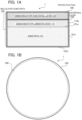
- Fig. 1A is a schematic diagram showing a cross section of a substrate unit 1 according to a first embodiment
- Fig. 1B is a schematic diagram showing an upper surface of the substrate unit 1.
- the substrate unit 1 includes a multilayer substrate 100 including a plurality of semiconductor layers stacked up and a protective film 109 covering the whole of the multilayer substrate 100.
- the multilayer substrate 100 includes a substrate 101 that is a semiconductor substrate (e.g., semiconductor wafer), a semiconductor laminated body 110 provided on the substrate 101, a sacrificial layer 105 provided on the semiconductor laminated body 110, and a semiconductor functional layer 120 provided on the sacrificial layer 105.
- a semiconductor substrate e.g., semiconductor wafer
- semiconductor laminated body 110 provided on the substrate 101
- a sacrificial layer 105 provided on the semiconductor laminated body 110
- a semiconductor functional layer 120 provided on the sacrificial layer 105.
- the semiconductor laminated body 110 includes one or a plurality of semiconductor layers formed on the substrate 101 by epitaxial growth as crystal growth. A concrete example of the semiconductor laminated body 110 will be described later.
- the sacrificial layer 105 is a semiconductor layer formed on the semiconductor laminated body 110 by epitaxial growth as crystal growth.
- the sacrificial layer 105 is formed with a material that is easily etched by an etchant material used (i.e., that has higher etching speed than other layers). A concrete example of the sacrificial layer 105 will be described later.
- the semiconductor functional layer 120 is a semiconductor layer in which semiconductor elements are to be formed. From the semiconductor functional layer 120 shown in Fig. 1A , a plurality of semiconductor elements split and two-dimensionally arranged on the substrate 101 by processing (i.e., a plurality of split semiconductor functional layers 120) are formed. By etching the sacrificial layer 105, each of the plurality of semiconductor elements (i.e., each of the plurality of split semiconductor functional layers 120) can be separated (i.e., peeled off) from the semiconductor laminated body 110.
- Each of the semiconductor functional layers 120 has a function as a semiconductor device (e.g., a light source, an optical detector, an image sensor, or the like) or a semiconductor element (e.g., a light emitting element, a light receiving element, a piezoelectric element, or the like).
- the separated semiconductor functional layer 120 is lifted and conveyed by a moving device (not shown) and is stuck on a mounting substrate (not shown) by intermolecular force, for example.
- a moving device not shown
- a mounting substrate not shown
- the protective film 109 covers the whole of the multilayer substrate 100 in Fig. 1
- the protective film 109 does not necessarily need to cover the whole of the multilayer substrate 100. It is permissible if the protective film 109 has structure for covering parts repeatedly used for the formation of the semiconductor functional layer 120.
- the protective film 109 is desired to cover at least a back surface 101b of the substrate 101 different from a formation surface 101a on which the semiconductor laminated body 110 is formed, a side face 101c of the substrate 101, and a side face 110c of the semiconductor laminated body 110 on the substrate unit 1.
- the substrate unit 1 with the protective film 109 formed from the back surface 101b to a side face of a buffer layer 104 shown in FIG. 4 to FIG.
- the substrate 101 and a buffer layer 102 are never eroded in the etching processes after the formation and the separation of the semiconductor functional layer 120 and it becomes possible to repeatedly reuse the substrate 101 and the buffer layer 102 (shown in FIG. 4 to FIG. 16 described later).
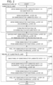
- Fig. 2 is a flowchart showing a manufacturing method of the substrate unit according to the first embodiment.
- Fig. 3, Fig. 4, and Fig. 5 are schematic cross-sectional views showing a manufacturing process (part 1, part 2 and part 3) of the substrate unit according to the first embodiment.
- the semiconductor laminated body 110 is grown on the substrate 101 as a semiconductor substrate by epitaxial growth (step S101 in Fig. 2 ), the sacrificial layer 105 is grown on the semiconductor laminated body 110 (step S102 in Fig. 2 ), and the semiconductor functional layer 120 is grown on the sacrificial layer 105 (step S103 in Fig. 2 ).
- the substrate 101 is an indium phosphide (InP) substrate, for example.
- the semiconductor laminated body 110 grown on the substrate 101 includes a buffer layer 102 as a first layer made with InP, an etching stop layer 103 as a second layer made with indium gallium arsenide (InGaAs) formed on the buffer layer 102, a buffer layer 104 as a third layer made with InP formed on the etching stop layer 103, and the sacrificial layer 105 made with indium gallium arsenide (InGaAs).
- the sacrificial layer 105 may be a single layer made with only InGaAs.
- the sacrificial layer 105 may be a multilayer structure formed with layers of multiple materials which include a layer made with InGaAs and another layer made with indium gallium arsenide phosphide (InGaAsP).
- Hydrochloric acid is used as an etchant material for the buffer layer 104 as a first etchant material, and a liquid mixture of phosphoric acid and a hydrogen peroxide solution, a liquid mixture of citric acid and a hydrogen peroxide solution, or a liquid mixture of sulfuric acid and a hydrogen peroxide solution is used as an etchant material for the etching stop layer 103 as a second etchant material.
- a liquid mixture of phosphoric acid and a hydrogen peroxide solution a liquid mixture of citric acid and a hydrogen peroxide solution, or a liquid mixture of sulfuric acid and a hydrogen peroxide solution is used.
- the buffer layer 102 By forming the buffer layer 102 with the same material as the substrate 101, the total thickness of the substrate 101 and the buffer layer 102 can be increased. Further, providing the buffer layer 102 makes it possible not to reduce the thickness of the substrate 101 also when removing upper layers in a reuse (i.e., recycling) process which will be described later.
- the etching stop layer 103 may also be formed with a different material such as aluminum gallium arsenide (AlGaAs) .
- AlGaAs aluminum gallium arsenide
- the semiconductor laminated body 110 is not limited to that having the configuration shown in Fig. 4 .
- the semiconductor functional layer 120 grown on the sacrificial layer 105 includes an n-type cladding layer 106 made with InP, an active layer 107 as an InGaAs photoabsorption layer, and a p-type cladding layer 108 made with InP.
- the n-type cladding layer 106 and the p-type cladding layer 108 are formed with the same material as the substrate 101.
- the protective film 109 covering the whole of the multilayer substrate 100 is formed (step S104 in Fig. 2 ).
- the protective film 109 is formed with organic metallic material, for example.
- the protective film 109 is formed by means of ALD (Atomic Layer Deposition), for example.
- the protective film 109 may also be formed by a different method such as CVD (Chemical Vapor Deposition) .
- the protective film 109 is formed to cover at least the back surface 101b of the substrate 101 opposite to the semiconductor laminated body 110, the side face 101c of the substrate 101, and the side face 110c of the semiconductor laminated body 110, as parts reused for the formation of the semiconductor functional layer 120.
- ALD ALD
- the film thickness of the protective film 109 can be uniformalized.
- TMA trimethylaluminum
- the protective film 109 can also be a resist or the like as a different organic protective film.
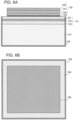
- Figs. 6A and 6B , Figs. 7A and 7B and Figs. 8A and 8B are schematic cross-sectional views and schematic plan views showing a peeling process (part 1, part 2 and part 3) of a semiconductor functional layer 120.
- Fig. 9 is a schematic cross-sectional view showing the peeling process (part 4) of the semiconductor functional layer. While the plan-view shape of the substrate 101 is shown as a square shape in these drawings, the plan-view shape is not limited to the illustrated example.
- the semiconductor functional layer 120 and the sacrificial layer 105 are patterned by means of dry etching as shown in Figs. 6A and 6B , and the p-type cladding layer 108 made with InP and the active layer 107 made with InGaAs are patterned by means of dry etching as shown in Figs. 7A and 7B (step S105 in Fig. 2 ) .
- a functional layer protective film 121 is formed to cover the side face of the active layer 107 and the upper surface and the side face of the p-type cladding layer 108 (step S106 in Fig. 2 ).
- the functional layer protective film 121 is formed with Al 2 O 3 , Si 3 N 4 , SiO 2 or the like, for example.
- the sacrificial layer 105 is etched by using an etchant material for wet etching, and the semiconductor functional layer 120 is lifted by the moving device (not shown) and thereby separated (i.e., peeled off) from the semiconductor laminated body 110 (step S107 in Fig. 2 ).
- the peeled semiconductor functional layer 120 e.g., an individual piece of the semiconductor functional layer 120
- a desired mounting substrate not shown
- functions as a semiconductor element e.g., a light emitting element, a light receiving element, a piezoelectric element, or the like.
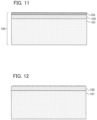
- Fig. 10 to Fig. 13 are schematic cross-sectional views showing a reuse process (part 1 to part 4) of the substrate unit according to the first embodiment. While the plan-view shape of the substrate 101 is shown as a square shape in these drawings, the plan-view shape is not limited to the illustrated example.
- the buffer layer 104 is wet etched until reaching a state in which the substrate 101, the buffer layer 102, the etching stop layer 103, and part of the protective film 109 remain unremoved. Subsequently, as shown in Fig. 11 , the protective film 109 is etched. It is also possible to leave the protective film 109 unremoved in Fig. 11 and Fig. 12 . Subsequently, as shown in Fig. 12 , the etching stop layer 103 is wet etched.
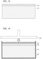
- Fig. 13 shows the multilayer substrate having the smoothed upper surface.
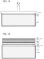
- Fi.g. 14 and Fig. 15 are schematic cross-sectional views showing a machine polishing process (part 1 and part 2) of the substrate unit according to the first embodiment.
- Fig. 14 and Fig. 15 show a modification of the process shown in Fig. 10 to Fig. 12 . That is, the process shown in Fig. 10 to Fig. 12 may be replaced with the machine polishing process by a polishing apparatus 150 shown in Fig. 14 and Fig. 15 .
- As the machine polishing CMP (Chemical Mechanical Polishing) is used, for example.
- CMP Chemical Mechanical Polishing
- Fig. 16 is a schematic cross-sectional view showing the reuse process (part 5) of the substrate unit according to the first embodiment.
- a buffer layer (a surface projecting upward relative to the protective film 109) is additionally formed on the buffer layer 102 in Fig. 15 , and the etching stop layer 103 and the buffer layer 104 as remaining layers of the semiconductor laminated body 110, the sacrificial layer 105, and the semiconductor functional layer 120 are successively grown (step S109 in Fig. 2 ).
- a buffer layer is additionally formed on the buffer layer 102 in Fig. 13 , and subsequent layers are formed again as shown in Fig. 4 .
- the semiconductor functional layer 120 and the sacrificial layer 105 are patterned by means of dry etching as shown in Figs. 6A and 6B , and the p-type cladding layer 108 made with InP and the active layer 107 made with InGaAs are patterned by means of dry etching as shown in Figs. 7A and 7B (step S110 in Fig. 2 ) .
- the functional layer protective film 121 is formed to cover the side face of the active layer 107 and the upper surface and the side face of the p-type cladding layer 108.
- the semiconductor functional layer 120 is peeled off from the semiconductor laminated body 110 (step Sill in Fig. 2 ).
- the process from the step S108 to the step S111 (i.e., the process for forming the semiconductor functional layer) can be executed repeatedly. Further, in the reuse process, the substrate unit in Fig. 5 can be obtained again by executing the ALD processing.
- the damage to the substrate 101 made with InP can be reduced thanks to the provision of the protective film 109. Further, it becomes possible to repeatedly reuse the substrate 101 and the buffer layer 102 in a state with no erosion of the buffer layer 102 made with InP. Therefore, the number of times of reusing the substrate 101 and the semiconductor laminated body 110 for growing the semiconductor functional layer 120 can be increased. Furthermore, in a case where the protective film 109 is formed after the semiconductor functional layer 120 is formed, the damage to the substrate 101 during the etching of the sacrificial layer 105 can be further reduced and the number of times of the reusing can be further increased.
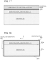
- Fig. 17 is a schematic diagram showing a multilayer substrate as an original form of a substrate unit according to a second embodiment.
- Fig. 18 is a schematic diagram showing a cross section of the substrate unit 2 according to the second embodiment.
- the substrate unit 2 in Fig. 18 is used for growing a semiconductor functional layer 220 shown in Fig. 17 .
- the substrate unit 2 in Fig. 18 is formed by reusing a substrate 201 and a semiconductor laminated body 210 after peeling off the semiconductor functional layer 220 in Fig. 17 .
- the substrate unit 2 includes a multilayer substrate 200 including a plurality of semiconductor layers stacked up and a protective film 209 covering the whole of the multilayer substrate 200.
- the multilayer substrate 200 includes the substrate 201 that is a semiconductor substrate (e.g., semiconductor wafer) and the semiconductor laminated body 210 provided on the substrate 201.
- the semiconductor laminated body 210 includes one or a plurality of semiconductor layers formed on the substrate 201 by epitaxial growth as crystal growth. A concrete example of the semiconductor laminated body 210 will be described later.
- a sacrificial layer 205 shown in Fig. 17 is a semiconductor layer formed on the semiconductor laminated body 210 by epitaxial growth as crystal growth.
- the sacrificial layer 205 is formed with a material that is easily etched by the etchant material used (i.e., that has a higher etching speed than other layers).
- a concrete example of the sacrificial layer 205 will be described later.
- the semiconductor functional layer 220 shown in Fig. 17 is a semiconductor layer in which semiconductor elements are to be formed. Similarly to the case in the first embodiment, the semiconductor functional layer 220 is split and two-dimensionally arranged on a semiconductor wafer by processing. By etching the sacrificial layer 205, each of the plurality of semiconductor elements (i.e., each of the plurality of split semiconductor functional layers 220) can be separated (i.e., peeled off) from the semiconductor laminated body 210.
- Each of the semiconductor functional layers 220 has a function as a semiconductor device (e.g., a light source, an optical detector, an image sensor, or the like) or a semiconductor element (e.g., a light emitting element, a light receiving element, a piezoelectric element, or the like).
- the separated semiconductor functional layer 220 is lifted and conveyed by the moving device (not shown) and is stuck on a mounting substrate (not shown) by intermolecular force, for example.
- a concrete example of the semiconductor functional layer 220 will be described later.
- the protective film 209 covers the whole of the multilayer substrate 200 in Fig. 18
- the protective film 209 does not necessarily need to cover the whole of the multilayer substrate 200. It is permissible if the protective film 209 has structure for covering parts repeatedly used for the formation of the semiconductor functional layer 220.
- the protective film 209 is desired to cover at least a back surface 201b of the substrate 201 from a formation surface 201a on which the semiconductor laminated body 210 is formed, a side face 201c of the substrate 201, and a side face 210c of the semiconductor laminated body 210 on the substrate unit 2.
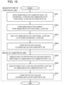
- Fig. 19 is a flowchart showing a manufacturing method of the substrate unit according to the second embodiment.
- Fig. 20 and Fig. 21 are schematic cross-sectional views showing a manufacturing process (part 1 and part 2) of the substrate unit according to the second embodiment.
- the semiconductor laminated body 210 is grown on the substrate 201 as the semiconductor substrate by epitaxial growth, the sacrificial layer 205 is grown on the semiconductor laminated body 210, and the semiconductor functional layer 220 is grown on the sacrificial layer 205 (step S201 in Fig . 19 ) .
- the substrate 201 is an InP substrate, for example.
- the sacrificial layer 105 may be a single layer made with only InGaAs.
- the sacrificial layer 105 may be a multilayer structure formed with layers of multiple materials which include a layer made with InGaAs and another layer made with InGaAsP.
- the semiconductor laminated body 210 grown on the substrate 201 includes a buffer layer 202 as a first layer made with InP, an etching stop layer 203 as a second layer made with InGaAs formed on the buffer layer 202, and a buffer layer 204 as a third layer made with InP formed on the etching stop layer 203.
- the buffer layer 202 By forming the buffer layer 202 with the same material as the substrate 201, the total thickness of the substrate 201 and the buffer layer 202 can be increased. Further, providing the buffer layer 202 makes it possible not to reduce the thickness of the substrate 201 also when removing upper layers in a reuse process which will be described later.
- the etching stop layer 203 may also be formed with a different material such as InGaAsP.
- the semiconductor laminated body 210 is not limited to that having the configuration shown in Fig. 21 .
- the semiconductor functional layer 220 grown on the sacrificial layer 205 includes an n-type cladding layer 206 made with InP, an active layer 207 as an InGaAs photoabsorption layer, and a p-type cladding layer 208 made with InP.
- the n-type cladding layer 206 and the p-type cladding layer 208 are formed with the same material as the substrate 201.
- Figs. 22A and 22B , Figs. 23A and 23B and Figs. 24A and 24B are schematic cross-sectional views and schematic plan views showing the manufacturing process (part 3, part 4 and part 5) of the substrate unit according to the second embodiment. While the plan-view shape of the substrate 201 is shown as a square shape in these drawings, the plan-view shape is not limited to the illustrated example.
- the semiconductor functional layer 220 and the sacrificial layer 105 are patterned by means of dry etching as shown in Figs. 22A and 22B , and the p-type cladding layer 208 made with InP and the active layer 207 made with InGaAs are patterned by means of dry etching as shown in Figs. 23A and 23B (step S202 in Fig. 19 ).
- a functional layer protective film 221 is formed to cover the side face of the active layer 207 and the upper surface and the side face of the p-type cladding layer 208.
- the functional layer protective film 221 is formed with Al 2 O 3 , Si 3 N 4 , SiO 2 or the like, for example.
- Fig. 25 is a schematic cross-sectional view showing the manufacturing process (part 7) of the substrate unit according to the second embodiment.
- the sacrificial layer 205 is etched by using an etchant material for wet etching, and the semiconductor functional layer 220 is lifted by the moving device (not shown) and thereby separated (i.e., peeled off) from the semiconductor laminated body 210 (step S203 in Fig. 19 ).
- the peeled semiconductor functional layer 220 (e.g., an individual piece of the semiconductor functional layer 220) is stuck on (i.e., transferred onto) a desired mounting substrate (not shown), provided with wiring, and functions as a semiconductor element (e.g., a light emitting element, a light receiving element, a piezoelectric element, or the like).
- a semiconductor element e.g., a light emitting element, a light receiving element, a piezoelectric element, or the like.
- Fig. 26 is a schematic cross-sectional view showing the manufacturing process (part 8) of the substrate unit according to the second embodiment.
- the protective film 209 covering the whole of the multilayer substrate 200 made up of the substrate 201 and the semiconductor laminated body 210 is formed (step S204 in Fig. 19 ).
- the protective film 209 is formed with organic metallic material, for example.
- the protective film 209 is formed by means of ALD, for example.
- the protective film 209 may also be formed by a different method such as CVD.
- the protective film 209 does not necessarily need to cover the whole of the multilayer substrate 200.
- the protective film 209 is formed to cover at least the back surface 201b of the substrate 201 opposite to the semiconductor laminated body 210, the side face 201c of the substrate 201, and the side face 210c of the semiconductor laminated body 210, as parts reused for the formation of the semiconductor functional layer 220.
- the protective film 209 is the same as the protective film in the first embodiment.
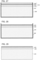
- Fig. 27 to Fig. 31 are schematic cross-sectional views showing a reuse process (part 1 to part 5) of the substrate unit according to the second embodiment.
- the buffer layer 204 is wet etched until reaching a state in which the substrate 201, the buffer layer 202, the etching stop layer 203, and part of the protective film 209 remain unremoved.
- the protective film 209 is etched. It is also possible to leave the protective film 209 unremoved in Fig. 29 .
- the etching stop layer 203 is wet etched.
- Fig. 31 shows the multilayer substrate having the smoothed upper surface. It is also possible to use CMP for the smoothing process similarly to the case in the first embodiment.
- Fig. 32 is a schematic cross-sectional view showing the reuse process (part 6) of the substrate unit according to the second embodiment.
- the multilayer substrate 200 is formed by successively growing the etching stop layer 203 and the buffer layer 204, as the remaining layers of the semiconductor laminated body 210, on the buffer layer 202 in Fig. 31 (step S206 in Fig. 19 ) .
- the protective film 209 covering the whole of the multilayer substrate 200 is formed (step S207 in Fig. 19 ) .
- the protective film 209 is formed to cover at least the back surface 201b of the substrate 201 opposite to the semiconductor laminated body 210, the side face 201c of the substrate 201, and the side face 210c of the semiconductor laminated body 210, as parts reused for the formation of the semiconductor functional layer 220.
- the substrate unit 2 shown in Fig. 26 is formed by this process.
- the semiconductor laminated body 110, 210 may be provided with an additional layer
- the sacrificial layer 105, 205 may be provided with an additional layer
- the semiconductor functional layer 120, 220 may be provided with an additional upper layer.
- the semiconductor laminated body 110 (210) is formed with the buffer layer 102 (202), the etching stop layer 103 (203) and the buffer layer 104 (204)
- the semiconductor laminated body 110 (210) may also be formed with only one layer.
- the semiconductor laminated body may be formed with only the buffer layer 104 (204).
- the multilayer substrate 100, 200 may also be formed by using GaAs-based materials or GaN-based materials.
- GaAs as the material of the substrate 101, 201
- GaAs as the material of the buffer layer 102, 202
- InGaP as the material of the etching stop layer 103, 203
- AlGaAs or GaAs as the material of the buffer layer 104, 204
- AlAs as the material of the sacrificial layer 105, 205 .
- a substrate unit according to the modification 2 by using a multilayer substrate 1100 that includes a semiconductor laminated body 1110 including a buffer layer 1102 made of InP and an etching stop layer 1103 made of InGaAs; a sacrificial layer 1105 made of InP; and a semiconductor functional layer 1120 including an n-type cladding layer 1106 made of InGaAs, an active layer (AC) 1107, and a p-type cladding layer 1108 made of InGaAs.
- a multilayer substrate 1100 that includes a semiconductor laminated body 1110 including a buffer layer 1102 made of InP and an etching stop layer 1103 made of InGaAs; a sacrificial layer 1105 made of InP; and a semiconductor functional layer 1120 including an n-type cladding layer 1106 made of InGaAs, an active layer (AC) 1107, and a p-type cladding layer 1108 made of InGaAs.
- AC active layer
- a protective film 1109 is formed.
- the materials, shape, and formation method of the protective film 1109 are substantially the same as those of the protective film 109 in the first embodiment.
- the sacrificial layer 1105 is removed and the semiconductor functional layer 1120 is separated from the semiconductor laminated body 1110, as in the first or second embodiment. Thereafter, similarly to the case shown in Figs.
- the etching stop layer 1103 is removed by polishing by CMP and an upper surface of the buffer layer 1102 is smoothed, thereby obtaining the substrate unit that includes the substrate 1101, the buffer layer 1102 having a smoothed upper surface and formed on the substrate 1101, and the protective film 1109 configured to cover from a back surface 1101b and a side face 1101c of the substrate 1101 to a side face 1102c of the buffer layer 1102 (the side faces 1101c and 1102c forms a side face of the semiconductor laminated body 1110).
Landscapes
- Recrystallisation Techniques (AREA)
- Weting (AREA)
- Laminated Bodies (AREA)
Abstract
Description
- The present disclosure relates to a manufacturing method of a substrate unit and to a substrate unit.
- There has been proposed a technology regarding a manufacturing method of a semiconductor device that makes it possible to reuse a substrate for the crystal growth of a semiconductor thin film as a semiconductor functional layer (see
Patent Reference 1, for example). -
Patent Reference 1 isJapanese Patent Application Publication No. 2005-019590 - However, damage to the substrate in an etching process cannot be prevented adequately by just protecting the substrate's crystal growth surface as in the aforementioned conventional technology. Therefore, a multilayer substrate including the substrate and a semiconductor laminated body formed on the substrate cannot be reused for the crystal growth of the next semiconductor functional layer in many cases.
- An object of the present disclosure is to provide a manufacturing method of a substrate unit and a substrate unit capable of reducing damage to a substrate for the growth of a semiconductor functional layer.
- A manufacturing method of a substrate unit according to the present disclosure, includes forming a semiconductor laminated body on a substrate; forming a sacrificial layer on the semiconductor laminated body; forming a semiconductor functional layer on the sacrificial layer; and forming a protective film that covers at least a back surface of the substrate different from a formation surface on which the semiconductor laminated body is formed, a side face of the substrate, and a side face of the semiconductor laminated body.
- A substrate unit according to the present disclosure, includes a substrate; a semiconductor laminated body formed on the substrate; and a protective film that covers at least a back surface of the substrate different from a formation surface on which the semiconductor laminated body is formed, a side face of the substrate, and a side face of the semiconductor laminated body.
- According to the present disclosure, the damage to the substrate for the growth of the semiconductor functional layer can be reduced and the number of times of reusing the substrate and the semiconductor laminated body can be increased.
-
-
Fig. 1A is a schematic diagram showing a cross section of a substrate unit according to a first embodiment, andFig. 1B is a schematic diagram showing an upper surface of the substrate unit according to the first embodiment; -
Fig. 2 is a flowchart showing a manufacturing method of the substrate unit according to the first embodiment; -
Fig. 3 is a schematic cross-sectional view showing a manufacturing process (part 1) of the substrate unit according to the first embodiment; -
Fig. 4 is a schematic cross-sectional view showing the manufacturing process (part 2) of the substrate unit according to the first embodiment; -
Fig. 5 is a schematic cross-sectional view showing the manufacturing process (part 3) of the substrate unit according to the first embodiment; -
Figs. 6A and 6B are a schematic cross-sectional view and a schematic plan view showing a peeling process (part 1) of a semiconductor functional layer; -
Figs. 7A and 7B are a schematic cross-sectional view and a schematic plan view showing the peeling process (part 2) of the semiconductor functional layer; -
Figs. 8A and 8B are a schematic cross-sectional view and a schematic plan view showing the peeling process (part 3) of the semiconductor functional layer; -
Fig. 9 is a schematic cross-sectional view showing the peeling process (part 4) of the semiconductor functional layer; -
Fig. 10 is a schematic cross-sectional view showing a reuse process (part 1) of the substrate unit according to the first embodiment; -
Fig. 11 is a schematic cross-sectional view showing the reuse process (part 2) of the substrate unit according to the first embodiment; -
Fig. 12 is a schematic cross-sectional view showing the reuse process (part 3) of the substrate unit according to the first embodiment; -
Fig. 13 is a schematic cross-sectional view showing the reuse process (part 4) of the substrate unit according to the first embodiment; -
Fig. 14 is a schematic cross-sectional view showing a machine polishing process (part 1) of the substrate unit according to the first embodiment; -
Fig. 15 is a schematic cross-sectional view showing the machine polishing process (part 2) of the substrate unit according to the first embodiment; -
Fig. 16 is a schematic cross-sectional view showing the reuse process (part 5) of the substrate unit according to the first embodiment; -
Fig. 17 is a schematic diagram showing a multilayer substrate as an original form of a substrate unit according to a second embodiment; -
Fig. 18 is a schematic diagram showing a cross section of the substrate unit according to the second embodiment; -
Fig. 19 is a flowchart showing a manufacturing method of the substrate unit according to the second embodiment; -
Fig. 20 is a schematic cross-sectional view showing a manufacturing process (part 1) of the substrate unit according to the second embodiment; -
Fig. 21 is a schematic cross-sectional view showing the manufacturing process (part 2) of the substrate unit according to the second embodiment; -
Figs. 22A and 22B are a schematic cross-sectional view and a schematic plan view showing the manufacturing process (part 3) of the substrate unit according to the second embodiment; -
Figs. 23A and 23B are a schematic cross-sectional view and a schematic plan view showing the manufacturing process (part 4) of the substrate unit according to the second embodiment; -
Figs. 24A and 24B are a schematic cross-sectional view and a schematic plan view showing the manufacturing process (part 5) of the substrate unit according to the second embodiment; -
Fig. 25 is a schematic cross-sectional view showing the manufacturing process (part 6) of the substrate unit according to the second embodiment; -
Fig. 26 is a schematic cross-sectional view showing the manufacturing process (part 7) of the substrate unit according to the second embodiment; -
Fig. 27 is a schematic cross-sectional view showing a reuse process (part 1) of the substrate unit according to the second embodiment; -
Fig. 28 is a schematic cross-sectional view showing the reuse process (part 2) of the substrate unit according to the second embodiment; -
Fig. 29 is a schematic cross-sectional view showing the reuse process (part 3) of the substrate unit according to the second embodiment; -
Fig. 30 is a schematic cross-sectional view showing the reuse process (part 4) of the substrate unit according to the second embodiment; -
Fig. 31 is a schematic cross-sectional view showing the reuse process (part 5) of the substrate unit according to the second embodiment; -
Fig. 32 is a schematic cross-sectional view showing the reuse process (part 6) of the substrate unit according to the second embodiment; -
Fig. 33 is a schematic diagram showing a cross section of a multilayer substrate as an original form of a substrate unit according to amodification 2 of the first embodiment; and -
Fig. 34 is a schematic diagram showing a cross section of a substrate unit according to themodification 2 of the first embodiment. - A manufacturing method of a substrate unit and a substrate unit according to each embodiment of the present disclosure will be described below with reference to the drawings. The following embodiments are just examples and a variety of modifications are possible within the scope of the present disclosure.
-
Fig. 1A is a schematic diagram showing a cross section of asubstrate unit 1 according to a first embodiment, andFig. 1B is a schematic diagram showing an upper surface of thesubstrate unit 1. - The
substrate unit 1 includes amultilayer substrate 100 including a plurality of semiconductor layers stacked up and aprotective film 109 covering the whole of themultilayer substrate 100. Themultilayer substrate 100 includes asubstrate 101 that is a semiconductor substrate (e.g., semiconductor wafer), a semiconductorlaminated body 110 provided on thesubstrate 101, asacrificial layer 105 provided on the semiconductor laminatedbody 110, and a semiconductorfunctional layer 120 provided on thesacrificial layer 105. - The semiconductor laminated
body 110 includes one or a plurality of semiconductor layers formed on thesubstrate 101 by epitaxial growth as crystal growth. A concrete example of the semiconductor laminatedbody 110 will be described later. - The
sacrificial layer 105 is a semiconductor layer formed on the semiconductor laminatedbody 110 by epitaxial growth as crystal growth. Thesacrificial layer 105 is formed with a material that is easily etched by an etchant material used (i.e., that has higher etching speed than other layers). A concrete example of thesacrificial layer 105 will be described later. - The semiconductor
functional layer 120 is a semiconductor layer in which semiconductor elements are to be formed. From the semiconductorfunctional layer 120 shown inFig. 1A , a plurality of semiconductor elements split and two-dimensionally arranged on thesubstrate 101 by processing (i.e., a plurality of split semiconductor functional layers 120) are formed. By etching thesacrificial layer 105, each of the plurality of semiconductor elements (i.e., each of the plurality of split semiconductor functional layers 120) can be separated (i.e., peeled off) from the semiconductor laminatedbody 110. Each of the semiconductorfunctional layers 120 has a function as a semiconductor device (e.g., a light source, an optical detector, an image sensor, or the like) or a semiconductor element (e.g., a light emitting element, a light receiving element, a piezoelectric element, or the like). The separated semiconductorfunctional layer 120 is lifted and conveyed by a moving device (not shown) and is stuck on a mounting substrate (not shown) by intermolecular force, for example. A concrete example of the semiconductorfunctional layer 120 will be described later. - While the
protective film 109 covers the whole of themultilayer substrate 100 inFig. 1 , theprotective film 109 does not necessarily need to cover the whole of themultilayer substrate 100. It is permissible if theprotective film 109 has structure for covering parts repeatedly used for the formation of the semiconductorfunctional layer 120. For example, theprotective film 109 is desired to cover at least aback surface 101b of thesubstrate 101 different from aformation surface 101a on which the semiconductor laminatedbody 110 is formed, aside face 101c of thesubstrate 101, and aside face 110c of the semiconductor laminatedbody 110 on thesubstrate unit 1. In other words, thesubstrate unit 1 with theprotective film 109 formed from theback surface 101b to a side face of a buffer layer 104 (shown inFIG. 4 to FIG. 9 described later) is also permissible. With such asubstrate unit 1, thesubstrate 101 and abuffer layer 102 are never eroded in the etching processes after the formation and the separation of the semiconductorfunctional layer 120 and it becomes possible to repeatedly reuse thesubstrate 101 and the buffer layer 102 (shown inFIG. 4 to FIG. 16 described later). -
Fig. 2 is a flowchart showing a manufacturing method of the substrate unit according to the first embodiment.Fig. 3, Fig. 4, and Fig. 5 are schematic cross-sectional views showing a manufacturing process (part 1,part 2 and part 3) of the substrate unit according to the first embodiment. - As shown in
Fig. 3 and Fig. 4 , in the manufacturing method of the substrate unit according to the first embodiment, the semiconductor laminatedbody 110 is grown on thesubstrate 101 as a semiconductor substrate by epitaxial growth (step S101 inFig. 2 ), thesacrificial layer 105 is grown on the semiconductor laminated body 110 (step S102 inFig. 2 ), and the semiconductorfunctional layer 120 is grown on the sacrificial layer 105 (step S103 inFig. 2 ). Thesubstrate 101 is an indium phosphide (InP) substrate, for example. - As shown in
Fig. 4 , the semiconductor laminatedbody 110 grown on thesubstrate 101 includes abuffer layer 102 as a first layer made with InP, anetching stop layer 103 as a second layer made with indium gallium arsenide (InGaAs) formed on thebuffer layer 102, abuffer layer 104 as a third layer made with InP formed on theetching stop layer 103, and thesacrificial layer 105 made with indium gallium arsenide (InGaAs). Thesacrificial layer 105 may be a single layer made with only InGaAs. Alternatively, thesacrificial layer 105 may be a multilayer structure formed with layers of multiple materials which include a layer made with InGaAs and another layer made with indium gallium arsenide phosphide (InGaAsP). Hydrochloric acid is used as an etchant material for thebuffer layer 104 as a first etchant material, and a liquid mixture of phosphoric acid and a hydrogen peroxide solution, a liquid mixture of citric acid and a hydrogen peroxide solution, or a liquid mixture of sulfuric acid and a hydrogen peroxide solution is used as an etchant material for theetching stop layer 103 as a second etchant material. Also, for thesacrificial layer 105, a liquid mixture of phosphoric acid and a hydrogen peroxide solution, a liquid mixture of citric acid and a hydrogen peroxide solution, or a liquid mixture of sulfuric acid and a hydrogen peroxide solution is used. - By forming the
buffer layer 102 with the same material as thesubstrate 101, the total thickness of thesubstrate 101 and thebuffer layer 102 can be increased. Further, providing thebuffer layer 102 makes it possible not to reduce the thickness of thesubstrate 101 also when removing upper layers in a reuse (i.e., recycling) process which will be described later. Theetching stop layer 103 may also be formed with a different material such as aluminum gallium arsenide (AlGaAs) . The semiconductor laminatedbody 110 is not limited to that having the configuration shown inFig. 4 . - As shown in
Fig. 4 , the semiconductorfunctional layer 120 grown on thesacrificial layer 105 includes an n-type cladding layer 106 made with InP, anactive layer 107 as an InGaAs photoabsorption layer, and a p-type cladding layer 108 made with InP. In the first embodiment, the n-type cladding layer 106 and the p-type cladding layer 108 are formed with the same material as thesubstrate 101. - Subsequently, as shown in
Fig. 5 , theprotective film 109 covering the whole of themultilayer substrate 100 is formed (step S104 inFig. 2 ). Theprotective film 109 is formed with organic metallic material, for example. Theprotective film 109 is formed by means of ALD (Atomic Layer Deposition), for example. Theprotective film 109 may also be formed by a different method such as CVD (Chemical Vapor Deposition) . Theprotective film 109 is formed to cover at least theback surface 101b of thesubstrate 101 opposite to the semiconductor laminatedbody 110, theside face 101c of thesubstrate 101, and theside face 110c of the semiconductor laminatedbody 110, as parts reused for the formation of the semiconductorfunctional layer 120. When ALD is used, the film thickness of theprotective film 109 can be uniformalized. - Subsequently, when alumina as an oxidized film of aluminum is deposited as the
protective film 109 on the entire periphery of themultilayer substrate 100 by the ALD processing, if trimethylaluminum (TMA) is poured to flow on a planar material, TMA covers the surface of the planar material; however, TMA is not stacked further after the entire surface is covered with one layer of TMA. At this point, if nitrogen is poured, surplus TMA can be removed, and if water or ozone is poured next, methyl groups of TMA are separated, aluminum is oxidized, and one layer of alumina film is formed. - Subsequently, remaining water and ozone are removed and thereafter TMA is supplied again. By repeating this operation, a plurality of atomic layers of alumina are deposited. While trimethylaluminum is used in the first embodiment, it is also possible to use a different organic metal such as (CH3)3Ga (trimethylgallium) or the like, for example.
- The
protective film 109 can also be a resist or the like as a different organic protective film. -
Figs. 6A and 6B ,Figs. 7A and 7B andFigs. 8A and 8B are schematic cross-sectional views and schematic plan views showing a peeling process (part 1,part 2 and part 3) of a semiconductorfunctional layer 120.Fig. 9 is a schematic cross-sectional view showing the peeling process (part 4) of the semiconductor functional layer. While the plan-view shape of thesubstrate 101 is shown as a square shape in these drawings, the plan-view shape is not limited to the illustrated example. - Subsequently, the semiconductor
functional layer 120 and thesacrificial layer 105 are patterned by means of dry etching as shown inFigs. 6A and 6B , and the p-type cladding layer 108 made with InP and theactive layer 107 made with InGaAs are patterned by means of dry etching as shown inFigs. 7A and 7B (step S105 inFig. 2 ) . - Subsequently, as shown in
Figs. 8A and 8B , a functional layerprotective film 121 is formed to cover the side face of theactive layer 107 and the upper surface and the side face of the p-type cladding layer 108 (step S106 inFig. 2 ). The functional layerprotective film 121 is formed with Al2O3, Si3N4, SiO2 or the like, for example. - Subsequently, as shown in
Fig. 9 , thesacrificial layer 105 is etched by using an etchant material for wet etching, and the semiconductorfunctional layer 120 is lifted by the moving device (not shown) and thereby separated (i.e., peeled off) from the semiconductor laminated body 110 (step S107 inFig. 2 ). The peeled semiconductor functional layer 120 (e.g., an individual piece of the semiconductor functional layer 120) is stuck on (i.e., transferred onto) a desired mounting substrate (not shown), provided with wiring, and functions as a semiconductor element (e.g., a light emitting element, a light receiving element, a piezoelectric element, or the like). -
Fig. 10 to Fig. 13 are schematic cross-sectional views showing a reuse process (part 1 to part 4) of the substrate unit according to the first embodiment. While the plan-view shape of thesubstrate 101 is shown as a square shape in these drawings, the plan-view shape is not limited to the illustrated example. - After the semiconductor
functional layer 120 is peeled off from the semiconductor laminatedbody 110, as shown inFig. 10 , thebuffer layer 104 is wet etched until reaching a state in which thesubstrate 101, thebuffer layer 102, theetching stop layer 103, and part of theprotective film 109 remain unremoved. Subsequently, as shown inFig. 11 , theprotective film 109 is etched. It is also possible to leave theprotective film 109 unremoved inFig. 11 and Fig. 12 . Subsequently, as shown inFig. 12 , theetching stop layer 103 is wet etched. At that time, the exposed upper surface of thebuffer layer 102 is in a rough condition with low smoothness, and thus processing for smoothing is executed by a polishing process (lapping) (step S108 inFig. 2 ).Fig. 13 shows the multilayer substrate having the smoothed upper surface. - Fi.g. 14 and
Fig. 15 are schematic cross-sectional views showing a machine polishing process (part 1 and part 2) of the substrate unit according to the first embodiment.Fig. 14 andFig. 15 show a modification of the process shown inFig. 10 to Fig. 12 . That is, the process shown inFig. 10 to Fig. 12 may be replaced with the machine polishing process by apolishing apparatus 150 shown inFig. 14 andFig. 15 . As the machine polishing, CMP (Chemical Mechanical Polishing) is used, for example. By the machine polishing process shown inFig. 14 andFig. 15 , the multilayer substrate having the smoothed upper surface is obtained. -
Fig. 16 is a schematic cross-sectional view showing the reuse process (part 5) of the substrate unit according to the first embodiment. As shown inFig. 16 , a buffer layer (a surface projecting upward relative to the protective film 109) is additionally formed on thebuffer layer 102 inFig. 15 , and theetching stop layer 103 and thebuffer layer 104 as remaining layers of the semiconductor laminatedbody 110, thesacrificial layer 105, and the semiconductorfunctional layer 120 are successively grown (step S109 inFig. 2 ). Alternatively, a buffer layer is additionally formed on thebuffer layer 102 inFig. 13 , and subsequent layers are formed again as shown inFig. 4 . - Subsequently, the semiconductor
functional layer 120 and thesacrificial layer 105 are patterned by means of dry etching as shown inFigs. 6A and 6B , and the p-type cladding layer 108 made with InP and theactive layer 107 made with InGaAs are patterned by means of dry etching as shown inFigs. 7A and 7B (step S110 inFig. 2 ) . - Subsequently, as shown in
Figs. 8A and 8B , the functional layerprotective film 121 is formed to cover the side face of theactive layer 107 and the upper surface and the side face of the p-type cladding layer 108. - Subsequently, as shown in
Fig. 9 , the semiconductorfunctional layer 120 is peeled off from the semiconductor laminated body 110 (step Sill inFig. 2 ). - In the reuse process of the substrate unit, the process from the step S108 to the step S111 (i.e., the process for forming the semiconductor functional layer) can be executed repeatedly. Further, in the reuse process, the substrate unit in
Fig. 5 can be obtained again by executing the ALD processing. - As described above, with the manufacturing method or the
substrate unit 1 in the first embodiment, the damage to thesubstrate 101 made with InP can be reduced thanks to the provision of theprotective film 109. Further, it becomes possible to repeatedly reuse thesubstrate 101 and thebuffer layer 102 in a state with no erosion of thebuffer layer 102 made with InP. Therefore, the number of times of reusing thesubstrate 101 and the semiconductor laminatedbody 110 for growing the semiconductorfunctional layer 120 can be increased. Furthermore, in a case where theprotective film 109 is formed after the semiconductorfunctional layer 120 is formed, the damage to thesubstrate 101 during the etching of thesacrificial layer 105 can be further reduced and the number of times of the reusing can be further increased. -
Fig. 17 is a schematic diagram showing a multilayer substrate as an original form of a substrate unit according to a second embodiment.Fig. 18 is a schematic diagram showing a cross section of thesubstrate unit 2 according to the second embodiment. Thesubstrate unit 2 inFig. 18 is used for growing a semiconductorfunctional layer 220 shown inFig. 17 . Alternatively, thesubstrate unit 2 inFig. 18 is formed by reusing asubstrate 201 and a semiconductorlaminated body 210 after peeling off the semiconductorfunctional layer 220 inFig. 17 . - The
substrate unit 2 includes amultilayer substrate 200 including a plurality of semiconductor layers stacked up and aprotective film 209 covering the whole of themultilayer substrate 200. Themultilayer substrate 200 includes thesubstrate 201 that is a semiconductor substrate (e.g., semiconductor wafer) and the semiconductor laminatedbody 210 provided on thesubstrate 201. - The semiconductor laminated
body 210 includes one or a plurality of semiconductor layers formed on thesubstrate 201 by epitaxial growth as crystal growth. A concrete example of the semiconductor laminatedbody 210 will be described later. - A
sacrificial layer 205 shown inFig. 17 is a semiconductor layer formed on the semiconductor laminatedbody 210 by epitaxial growth as crystal growth. Thesacrificial layer 205 is formed with a material that is easily etched by the etchant material used (i.e., that has a higher etching speed than other layers). A concrete example of thesacrificial layer 205 will be described later. - The semiconductor
functional layer 220 shown inFig. 17 is a semiconductor layer in which semiconductor elements are to be formed. Similarly to the case in the first embodiment, the semiconductorfunctional layer 220 is split and two-dimensionally arranged on a semiconductor wafer by processing. By etching thesacrificial layer 205, each of the plurality of semiconductor elements (i.e., each of the plurality of split semiconductor functional layers 220) can be separated (i.e., peeled off) from the semiconductor laminatedbody 210. Each of the semiconductorfunctional layers 220 has a function as a semiconductor device (e.g., a light source, an optical detector, an image sensor, or the like) or a semiconductor element (e.g., a light emitting element, a light receiving element, a piezoelectric element, or the like). The separated semiconductorfunctional layer 220 is lifted and conveyed by the moving device (not shown) and is stuck on a mounting substrate (not shown) by intermolecular force, for example. A concrete example of the semiconductorfunctional layer 220 will be described later. - While the
protective film 209 covers the whole of themultilayer substrate 200 inFig. 18 , theprotective film 209 does not necessarily need to cover the whole of themultilayer substrate 200. It is permissible if theprotective film 209 has structure for covering parts repeatedly used for the formation of the semiconductorfunctional layer 220. For example, theprotective film 209 is desired to cover at least aback surface 201b of thesubstrate 201 from aformation surface 201a on which the semiconductor laminatedbody 210 is formed, aside face 201c of thesubstrate 201, and a side face 210c of the semiconductor laminatedbody 210 on thesubstrate unit 2. -
Fig. 19 is a flowchart showing a manufacturing method of the substrate unit according to the second embodiment.Fig. 20 and Fig. 21 are schematic cross-sectional views showing a manufacturing process (part 1 and part 2) of the substrate unit according to the second embodiment. - As shown in
Fig. 20 and Fig. 21 , in the manufacturing method of the substrate unit according to the second embodiment, the semiconductor laminatedbody 210 is grown on thesubstrate 201 as the semiconductor substrate by epitaxial growth, thesacrificial layer 205 is grown on the semiconductor laminatedbody 210, and the semiconductorfunctional layer 220 is grown on the sacrificial layer 205 (step S201 inFig . 19 ) . Thesubstrate 201 is an InP substrate, for example. Similarly to the case in the first embodiment, thesacrificial layer 105 may be a single layer made with only InGaAs. Alternatively, thesacrificial layer 105 may be a multilayer structure formed with layers of multiple materials which include a layer made with InGaAs and another layer made with InGaAsP. - As shown in
Fig. 21 , the semiconductor laminatedbody 210 grown on thesubstrate 201 includes abuffer layer 202 as a first layer made with InP, anetching stop layer 203 as a second layer made with InGaAs formed on thebuffer layer 202, and abuffer layer 204 as a third layer made with InP formed on theetching stop layer 203. - By forming the
buffer layer 202 with the same material as thesubstrate 201, the total thickness of thesubstrate 201 and thebuffer layer 202 can be increased. Further, providing thebuffer layer 202 makes it possible not to reduce the thickness of thesubstrate 201 also when removing upper layers in a reuse process which will be described later. Theetching stop layer 203 may also be formed with a different material such as InGaAsP. The semiconductor laminatedbody 210 is not limited to that having the configuration shown inFig. 21 . In the second embodiment, it is desirable that thesacrificial layer 205 be made with InGaAs and theetching stop layer 203 be made with InGaAsP. This lowers the etching selectivity ratio of theetching stop layer 203 to thesacrificial layer 205, thus reducing the damage to theetching stop layer 203 when thesacrificial layer 205 is removed. - As shown in
Fig. 21 , the semiconductorfunctional layer 220 grown on thesacrificial layer 205 includes an n-type cladding layer 206 made with InP, anactive layer 207 as an InGaAs photoabsorption layer, and a p-type cladding layer 208 made with InP. In the second embodiment, the n-type cladding layer 206 and the p-type cladding layer 208 are formed with the same material as thesubstrate 201. -
Figs. 22A and 22B ,Figs. 23A and 23B andFigs. 24A and 24B are schematic cross-sectional views and schematic plan views showing the manufacturing process (part 3,part 4 and part 5) of the substrate unit according to the second embodiment. While the plan-view shape of thesubstrate 201 is shown as a square shape in these drawings, the plan-view shape is not limited to the illustrated example. - Subsequently, the semiconductor
functional layer 220 and thesacrificial layer 105 are patterned by means of dry etching as shown inFigs. 22A and 22B , and the p-type cladding layer 208 made with InP and theactive layer 207 made with InGaAs are patterned by means of dry etching as shown inFigs. 23A and 23B (step S202 inFig. 19 ). - Subsequently, as shown in
Figs. 24A and 24B , a functional layerprotective film 221 is formed to cover the side face of theactive layer 207 and the upper surface and the side face of the p-type cladding layer 208. The functional layerprotective film 221 is formed with Al2O3, Si3N4, SiO2 or the like, for example. -
Fig. 25 is a schematic cross-sectional view showing the manufacturing process (part 7) of the substrate unit according to the second embodiment. As shown inFig. 25 , thesacrificial layer 205 is etched by using an etchant material for wet etching, and the semiconductorfunctional layer 220 is lifted by the moving device (not shown) and thereby separated (i.e., peeled off) from the semiconductor laminated body 210 (step S203 inFig. 19 ). The peeled semiconductor functional layer 220 (e.g., an individual piece of the semiconductor functional layer 220) is stuck on (i.e., transferred onto) a desired mounting substrate (not shown), provided with wiring, and functions as a semiconductor element (e.g., a light emitting element, a light receiving element, a piezoelectric element, or the like). -
Fig. 26 is a schematic cross-sectional view showing the manufacturing process (part 8) of the substrate unit according to the second embodiment. As shown inFig. 26 , theprotective film 209 covering the whole of themultilayer substrate 200 made up of thesubstrate 201 and the semiconductor laminatedbody 210 is formed (step S204 inFig. 19 ). Theprotective film 209 is formed with organic metallic material, for example. Theprotective film 209 is formed by means of ALD, for example. Theprotective film 209 may also be formed by a different method such as CVD. Theprotective film 209 does not necessarily need to cover the whole of themultilayer substrate 200. Theprotective film 209 is formed to cover at least theback surface 201b of thesubstrate 201 opposite to the semiconductor laminatedbody 210, theside face 201c of thesubstrate 201, and the side face 210c of the semiconductor laminatedbody 210, as parts reused for the formation of the semiconductorfunctional layer 220. Theprotective film 209 is the same as the protective film in the first embodiment. -
Fig. 27 to Fig. 31 are schematic cross-sectional views showing a reuse process (part 1 to part 5) of the substrate unit according to the second embodiment. - After the semiconductor
functional layer 220 is peeled off from the semiconductor laminatedbody 210, as shown inFig. 27 and Fig. 28 , thebuffer layer 204 is wet etched until reaching a state in which thesubstrate 201, thebuffer layer 202, theetching stop layer 203, and part of theprotective film 209 remain unremoved. Subsequently, as shown inFig. 29 , theprotective film 209 is etched. It is also possible to leave theprotective film 209 unremoved inFig. 29 . Subsequently, as shown inFig. 30 , theetching stop layer 203 is wet etched. At that time, the exposed upper surface of thebuffer layer 202 is in a rough condition with low smoothness, and thus processing for smoothing is executed by a polishing process (lapping) (step S205 inFig. 19 ).Fig. 31 shows the multilayer substrate having the smoothed upper surface. It is also possible to use CMP for the smoothing process similarly to the case in the first embodiment. -
Fig. 32 is a schematic cross-sectional view showing the reuse process (part 6) of the substrate unit according to the second embodiment. As shown inFig. 32 , themultilayer substrate 200 is formed by successively growing theetching stop layer 203 and thebuffer layer 204, as the remaining layers of the semiconductor laminatedbody 210, on thebuffer layer 202 inFig. 31 (step S206 inFig. 19 ) . - Subsequently, as shown in
Fig. 26 , theprotective film 209 covering the whole of themultilayer substrate 200 is formed (step S207 inFig. 19 ) . Theprotective film 209 is formed to cover at least theback surface 201b of thesubstrate 201 opposite to the semiconductor laminatedbody 210, theside face 201c of thesubstrate 201, and the side face 210c of the semiconductor laminatedbody 210, as parts reused for the formation of the semiconductorfunctional layer 220. Thesubstrate unit 2 shown inFig. 26 is formed by this process. - As described above, with the manufacturing method or the
substrate unit 2 in the second embodiment, thanks to the provision of theprotective film 209, it becomes possible to repeatedly reuse thesubstrate 201 and thebuffer layer 202 in a state with absolutely no erosion of not only thesubstrate 201 made with InP but also thebuffer layer 202 made with InP. Therefore, the number of times of reusing thesubstrate 201 and the semiconductor laminatedbody 210 for growing the semiconductorfunctional layer 220 can be increased. Furthermore, since theprotective film 109 is formed after the process of separating the semiconductorfunctional layer 220 from the semiconductor laminatedbody 210, it is possible to reduce the occurrence of scratches on theprotective film 209 that may occur during the process of the separating. Therefore, in the process of reusing the substrate unit, it is possible to prevent the etching solution (i.e., etchant) from entering through the scratches in theprotective film 209, thereby improving the yield in reuse. - While an example is shown about the semiconductor
functional layer substrate body sacrificial layer body sacrificial layer functional layer - While examples of forming the
multilayer substrate multilayer substrate substrate buffer layer etching stop layer buffer layer sacrificial layer - In the first embodiment described above, the semiconductor laminated
body 110 includes thebuffer layer 102, theetching stop layer 103 as an InGaAs layer formed on thebuffer layer 102, and thebuffer layer 104 as an InP layer formed on theetching stop layer 103; thesacrificial layer 105 as an InGaAs layer; and the semiconductorfunctional layer 101 including the n-type cladding layer 106 as an InP layer formed on thesacrificial layer 105, the active layer (AC) 107, and the p-type cladding layer 108 as an InGaAs layer. However, as shown inFig. 33 , it is possible to manufacture a substrate unit according to themodification 2 by using amultilayer substrate 1100 that includes a semiconductorlaminated body 1110 including abuffer layer 1102 made of InP and anetching stop layer 1103 made of InGaAs; asacrificial layer 1105 made of InP; and a semiconductorfunctional layer 1120 including an n-type cladding layer 1106 made of InGaAs, an active layer (AC) 1107, and a p-type cladding layer 1108 made of InGaAs. - In the
modification 2, after the semiconductor laminatedbody 1110, thesacrificial layer 1105, and the semiconductorfunctional layer 1120 are stacked on asubstrate 1101 in this order, aprotective film 1109 is formed. The materials, shape, and formation method of theprotective film 1109 are substantially the same as those of theprotective film 109 in the first embodiment. In subsequent steps, thesacrificial layer 1105 is removed and the semiconductorfunctional layer 1120 is separated from the semiconductor laminatedbody 1110, as in the first or second embodiment. Thereafter, similarly to the case shown inFigs. 14 and15 , theetching stop layer 1103 is removed by polishing by CMP and an upper surface of thebuffer layer 1102 is smoothed, thereby obtaining the substrate unit that includes thesubstrate 1101, thebuffer layer 1102 having a smoothed upper surface and formed on thesubstrate 1101, and theprotective film 1109 configured to cover from aback surface 1101b and aside face 1101c of thesubstrate 1101 to aside face 1102c of the buffer layer 1102 (the side faces 1101c and 1102c forms a side face of the semiconductor laminated body 1110). - In this way, even when the
substrate 1101 and thesacrificial layer 1105 are made of the same material (for example, InP), since theprotective film 1109 is formed after the semiconductorfunctional layer 1120 is formed and before thesacrificial layer 105 is removed, theback surface 1101b and theside face 1101c of thesubstrate 1101 and theside face 1102c of the buffer layer 1102 (the side faces 1101c and 1102c forms a side face of the semiconductor laminated body 1110) are protected from the damage caused by the etchant used to remove thesacrificial layer 1105. - Further, it is possible to form the
multilayer substrate 1100 of themodification 2 using GaAs-based materials or GaN-based materials as in themodification 1. - 1, 2: substrate unit, 100, 200, 1100: multilayer substrate, 101, 201, 1101: substrate, 101a., 201a: formation surface, 101b, 201b, 1101b: back surface, 101c, 201c, 1101c: side face of substrate, 102, 202, 1102: buffer layer (first layer), 1102c: side face of buffer layer, 103, 203, 1103: etching stop layer (second layer), 104, 204: buffer layer (third layer), 105, 205, 1105: sacrificial layer, 106, 206, 1106: n-type cladding layer, 107, 207, 1107: active layer, 108, 208, 1108: p-type cladding layer, 109, 209, 1109: protective film, 110, 210, 1110: semiconductor laminated body, 110c, 210c: side face of semiconductor laminated body, 120, 220: semiconductor functional layer.
Claims (15)
- A manufacturing method of a substrate unit (1, 2), comprising:forming a semiconductor laminated body (110, 210, 1110) on a substrate (101, 201, 1101);forming a sacrificial layer (105, 205, 1105) on the semiconductor laminated body (110, 210, 1110);forming a semiconductor functional layer (120, 220, 1120) on the sacrificial layer (105, 205, 1105); andforming a protective film (109, 209, 1109) that covers at least a back surface (101b, 201b, 1101b) of the substrate (101, 201, 1101) different from a formation surface (101a, 201a) on which the semiconductor laminated body (110, 210, 1110) is formed, a side face (101c, 201c, 1101c) of the substrate (101, 201, 1101), and a side face (110c, 210c, 1101c) of the semiconductor laminated body (110, 210, 1110).
- The manufacturing method of a substrate unit (1, 2) according to claim 1, wherein the protective film (109, 209, 1109) is formed after the semiconductor functional layer (120, 220, 1120) is formed.
- The manufacturing method of a substrate unit (1, 2) according to claim 2, wherein the protective film (109, 209, 1109) is formed to cover an entire periphery of the substrate (101, 201, 1101), the semiconductor laminated body (110, 210, 1110), the sacrificial layer (105, 205, 1105), and the semiconductor functional layer (120, 220, 1120).
- The manufacturing method of a substrate unit (1, 2) according to any of the preceding claims, wherein the protective film (109, 209, 1109) is formed after the semiconductor functional layer (120, 220, 1120) is separated from the semiconductor laminated body (110, 210, 1110) by etching the sacrificial layer (105, 205, 1105).
- The manufacturing method of a substrate unit (1, 2) according to claim 4, wherein the protective film (109, 209, 1109) is formed to cover an entire periphery of the substrate (101, 201, 1110) and the semiconductor laminated body (110, 210, 1110).
- The manufacturing method of a substrate unit according to any of the preceding claims, wherein the formation of the semiconductor laminated body (1110) is executed byforming a first layer (1102) on the substrate (1101), andforming a second layer (1103) made with a material different from that of the first layer (1102), on the first layer (1102).
- The manufacturing method of a substrate unit according to claim 6, wherein the second layer (1103) is etched by using an etchant material after the protective film (1109) is formed.
- The manufacturing method of a substrate unit according to claim 7, wherein
after the second layer (1103) is etched, a surface of the first layer (1102) on which the second layer (1103) is to be formed is smoothed by means of machine polishing. - The manufacturing method of a substrate unit (1, 2) according to any of the preceding claims, wherein the formation of the semiconductor laminated body (110, 210) is executed byforming a first layer (102, 202) on the substrate (101, 201),forming a second layer (103, 203) made with a material different from that of the first layer (102, 202), on the first layer (102, 202), andforming a third layer (104, 204) made with a same material as the first layer (102, 202), on the second layer (103, 203).
- A manufacturing method of a substrate unit (1, 2), for a multilayer substrate including a substrate (101, 201, 1101) and a semiconductor laminated body (110, 210, 1110) formed on the substrate (101, 201, 1101), the method comprising:
forming a protective film (109, 209) that covers at least a back surface (101b, 201b, 1101b) of the substrate (101, 201, 1101) different from a formation surface (101a, 201a) on which the semiconductor laminated body (110, 210, 1110) is formed, a side face (101c, 201c, 1101c) of the substrate (101, 201, 1101), and a side face of the semiconductor laminated body (110, 210, 1110). - A substrate unit comprising:a substrate (101, 201, 1101);a semiconductor laminated body (110, 210, 1110) formed on the substrate (101, 201, 1101); anda protective film (109, 209, 1109) that covers at least a back surface (101b, 201b, 1101b) of the substrate (101, 201, 1101) different from a formation surface (101a, 201a) on which the semiconductor laminated body (110, 210, 1110) is formed, a side face (101c, 201c, 1101c) of the substrate (101, 201, 1101), and a side face (110c, 210c) of the semiconductor laminated body (110, 210, 1110).
- The substrate unit according to claim 11, wherein the protective film (109, 209, 1109) covers an entire periphery of the substrate (101, 201, 1101) and the semiconductor laminated body (110, 210, 1110).
- The substrate unit according to claim 11 or 12, further comprising:a sacrificial layer (105, 205, 1105) formed on the semiconductor laminated body (110, 210, 1110); anda semiconductor functional layer (120, 220, 1120) that is formed on the sacrificial layer (105, 205, 1105) and can be separated from the semiconductor laminated body (110, 210, 1110) by etching of the sacrificial layer (105, 205, 1105).
- The substrate unit according to claim 13, wherein the protective film (109, 209, 1109) covers an entire periphery of the substrate (101, 201, 1101), the semiconductor laminated body (110, 210, 1110), the sacrificial layer (105, 205, 1105), and the semiconductor functional layer (120, 220, 1120).
- The substrate unit according to any of claims 11 to 14, wherein the semiconductor laminated body (110, 210, 1110) is a buffer layer formed with a same material as the substrate (101, 201, 1101).
Applications Claiming Priority (1)
| Application Number | Priority Date | Filing Date | Title |
|---|---|---|---|
| JP2023051481 | 2023-03-28 |
Publications (1)
| Publication Number | Publication Date |
|---|---|
| EP4439644A1 true EP4439644A1 (en) | 2024-10-02 |
Family
ID=89663482
Family Applications (1)
| Application Number | Title | Priority Date | Filing Date |
|---|---|---|---|
| EP24153031.0A Pending EP4439644A1 (en) | 2023-03-28 | 2024-01-22 | Manufacturing method of substrate unit, and substrate unit |
Country Status (5)
| Country | Link |
|---|---|
| US (1) | US20240332080A1 (en) |
| EP (1) | EP4439644A1 (en) |
| JP (1) | JP2024144108A (en) |
| CN (1) | CN118737811A (en) |
| TW (1) | TWI883799B (en) |
Families Citing this family (1)
| Publication number | Priority date | Publication date | Assignee | Title |
|---|---|---|---|---|
| JP2026090797A (en) * | 2024-11-22 | 2026-06-03 | 沖電気工業株式会社 | Semiconductor structure, method for manufacturing a semiconductor structure, and method for manufacturing an electronic device |
Citations (9)
| Publication number | Priority date | Publication date | Assignee | Title |
|---|---|---|---|---|
| JP2005019590A (en) | 2003-06-25 | 2005-01-20 | Oki Data Corp | Manufacturing method of semiconductor device |
| WO2008044381A1 (en) * | 2006-10-13 | 2008-04-17 | Omron Corporation | Vibration sensor and method for manufacturing the vibration sensor |
| US8895406B2 (en) * | 2006-09-20 | 2014-11-25 | The Board Of Trustees Of The University Of Illinois | Release strategies for making transferable semiconductor structures, devices and device components |
| US9548218B2 (en) * | 2012-02-07 | 2017-01-17 | The Regents Of The University Of Michigan | Thermal surface treatment for reuse of wafers after epitaxial lift off |
| US20170110314A1 (en) * | 2015-10-19 | 2017-04-20 | Quora Technology, Inc. | Lift Off Process for Chip Scale Package Solid State Devices on Engineered Substrate |
| CN112164707A (en) * | 2020-08-31 | 2021-01-01 | 福建华佳彩有限公司 | A kind of preparation method of flexible display panel |
| US10910272B1 (en) * | 2019-10-22 | 2021-02-02 | Sandisk Technologies Llc | Reusable support substrate for formation and transfer of semiconductor devices and methods of using the same |
| US20220359273A1 (en) * | 2018-08-29 | 2022-11-10 | Taiwan Semiconductor Manufacturing Company, Ltd. | Method for forming a semiconductor-on-insulator (soi) substrate |
| US20230065473A1 (en) * | 2021-08-30 | 2023-03-02 | Taiwan Semiconductor Manufacturing Company, Ltd. | Manufacturing method of semiconductor device |
Family Cites Families (3)
| Publication number | Priority date | Publication date | Assignee | Title |
|---|---|---|---|---|
| WO2014020906A1 (en) * | 2012-07-30 | 2014-02-06 | 住友化学株式会社 | Method for manufacturing composite substrate and method for manufacturing semiconductor crystal layer formation substrate |
| CN109791962B (en) * | 2017-08-24 | 2021-07-09 | 创光科学株式会社 | Method for producing nitride semiconductor ultraviolet light emitting element and nitride semiconductor ultraviolet light emitting element |
| US11961765B2 (en) * | 2019-05-23 | 2024-04-16 | Mitsubishi Electric Corporation | Method for manufacturing a semiconductor substrate and device by bonding an epitaxial substrate to a first support substrate, forming a first and second protective thin film layer, and exposing and bonding a nitride semiconductor layer to a second support substrate |
-
2024
- 2024-01-12 CN CN202410054660.1A patent/CN118737811A/en active Pending
- 2024-01-18 JP JP2024006066A patent/JP2024144108A/en active Pending
- 2024-01-19 US US18/417,365 patent/US20240332080A1/en active Pending
- 2024-01-22 EP EP24153031.0A patent/EP4439644A1/en active Pending
- 2024-01-25 TW TW113102890A patent/TWI883799B/en active
Patent Citations (9)
| Publication number | Priority date | Publication date | Assignee | Title |
|---|---|---|---|---|
| JP2005019590A (en) | 2003-06-25 | 2005-01-20 | Oki Data Corp | Manufacturing method of semiconductor device |
| US8895406B2 (en) * | 2006-09-20 | 2014-11-25 | The Board Of Trustees Of The University Of Illinois | Release strategies for making transferable semiconductor structures, devices and device components |
| WO2008044381A1 (en) * | 2006-10-13 | 2008-04-17 | Omron Corporation | Vibration sensor and method for manufacturing the vibration sensor |
| US9548218B2 (en) * | 2012-02-07 | 2017-01-17 | The Regents Of The University Of Michigan | Thermal surface treatment for reuse of wafers after epitaxial lift off |
| US20170110314A1 (en) * | 2015-10-19 | 2017-04-20 | Quora Technology, Inc. | Lift Off Process for Chip Scale Package Solid State Devices on Engineered Substrate |
| US20220359273A1 (en) * | 2018-08-29 | 2022-11-10 | Taiwan Semiconductor Manufacturing Company, Ltd. | Method for forming a semiconductor-on-insulator (soi) substrate |
| US10910272B1 (en) * | 2019-10-22 | 2021-02-02 | Sandisk Technologies Llc | Reusable support substrate for formation and transfer of semiconductor devices and methods of using the same |
| CN112164707A (en) * | 2020-08-31 | 2021-01-01 | 福建华佳彩有限公司 | A kind of preparation method of flexible display panel |
| US20230065473A1 (en) * | 2021-08-30 | 2023-03-02 | Taiwan Semiconductor Manufacturing Company, Ltd. | Manufacturing method of semiconductor device |
Also Published As
| Publication number | Publication date |
|---|---|
| TWI883799B (en) | 2025-05-11 |
| JP2024144108A (en) | 2024-10-11 |
| US20240332080A1 (en) | 2024-10-03 |
| CN118737811A (en) | 2024-10-01 |
| TW202439449A (en) | 2024-10-01 |
Similar Documents
| Publication | Publication Date | Title |
|---|---|---|
| US6100104A (en) | Method for fabricating a plurality of semiconductor bodies | |
| US9570351B2 (en) | Reusable semiconductor substrates | |
| EP2249401A1 (en) | Solar cell and method for manufacturing solar cell | |
| KR20180096579A (en) | Lift off process for chip scale package solid state devices on fabricated substrates | |
| US8330036B1 (en) | Method of fabrication and structure for multi-junction solar cell formed upon separable substrate | |
| US20240332080A1 (en) | Manufacturing method of substrate unit, and substrate unit | |
| JP4315744B2 (en) | LAMINATE AND SEMICONDUCTOR DEVICE MANUFACTURING METHOD | |
| US5288657A (en) | Device fabrication | |
| KR20160047759A (en) | Method of fabrication and structure for multi-junction solar cell formed upon separable substrate | |
| JP5394091B2 (en) | Manufacturing method of semiconductor device | |
| US20120322267A1 (en) | Method of patterning a substrate | |
| US11295950B2 (en) | Structure comprising single-crystal semiconductor islands and process for making such a structure | |
| US20220290327A1 (en) | Semiconductor wafer and method for manufacturing same | |
| US5327450A (en) | Optical semiconductor device and process of prodcuing same | |
| CN117543340A (en) | Epitaxial structure of semiconductor laser and preparation method of semiconductor laser | |
| CN101752475A (en) | Light emitting diode structure and manufacturing method thereof | |
| US20240030381A1 (en) | Method for Producing a Semiconductor Body and Semicondcutor Arrangement | |
| US20210005444A1 (en) | Method for manufacturing a silicon on nitride substrate | |
| US12610630B2 (en) | Method of manufacturing a light-receiving element and light-receiving element | |
| US12276839B2 (en) | Manufacturing a semiconductor structure | |
| US20250293034A1 (en) | Method for producing a scribe line in a germanium semiconductor wafer with superimposed iii-v semiconductor layers | |
| US20240421243A1 (en) | Method for producing a trench in a iii-v multi-junction solar cell | |
| US20240186140A1 (en) | Method for Forming Mixed Substrate | |
| US20250226260A1 (en) | Method for forming hybrid substrate of soi wafer | |
| CN112993760B (en) | Semiconductor manufacturing method |
Legal Events
| Date | Code | Title | Description |
|---|---|---|---|
| PUAI | Public reference made under article 153(3) epc to a published international application that has entered the european phase |
Free format text: ORIGINAL CODE: 0009012 |
|
| STAA | Information on the status of an ep patent application or granted ep patent |
Free format text: STATUS: THE APPLICATION HAS BEEN PUBLISHED |
|
| AK | Designated contracting states |
Kind code of ref document: A1 Designated state(s): AL AT BE BG CH CY CZ DE DK EE ES FI FR GB GR HR HU IE IS IT LI LT LU LV MC ME MK MT NL NO PL PT RO RS SE SI SK SM TR |
|
| STAA | Information on the status of an ep patent application or granted ep patent |
Free format text: STATUS: REQUEST FOR EXAMINATION WAS MADE |
|
| 17P | Request for examination filed |
Effective date: 20250402 |
|
| STAA | Information on the status of an ep patent application or granted ep patent |
Free format text: STATUS: EXAMINATION IS IN PROGRESS |
|
| 17Q | First examination report despatched |
Effective date: 20260410 |