EP4439537A1 - Pixel driving circuit, pixel driving method and display panel - Google Patents
Pixel driving circuit, pixel driving method and display panel Download PDFInfo
- Publication number
- EP4439537A1 EP4439537A1 EP23884137.3A EP23884137A EP4439537A1 EP 4439537 A1 EP4439537 A1 EP 4439537A1 EP 23884137 A EP23884137 A EP 23884137A EP 4439537 A1 EP4439537 A1 EP 4439537A1
- Authority
- EP
- European Patent Office
- Prior art keywords
- thin film
- film transistor
- supply voltage
- light
- node
- Prior art date
- Legal status (The legal status is an assumption and is not a legal conclusion. Google has not performed a legal analysis and makes no representation as to the accuracy of the status listed.)
- Pending
Links
Images



Classifications
-
- G—PHYSICS
- G09—EDUCATION; CRYPTOGRAPHY; DISPLAY; ADVERTISING; SEALS
- G09G—ARRANGEMENTS OR CIRCUITS FOR CONTROL OF INDICATING DEVICES USING STATIC MEANS TO PRESENT VARIABLE INFORMATION
- G09G3/00—Control arrangements or circuits, of interest only in connection with visual indicators other than cathode-ray tubes
- G09G3/20—Control arrangements or circuits, of interest only in connection with visual indicators other than cathode-ray tubes for presentation of an assembly of a number of characters, e.g. a page, by composing the assembly by combination of individual elements arranged in a matrix no fixed position being assigned to or needed to be assigned to the individual characters or partial characters
- G09G3/22—Control arrangements or circuits, of interest only in connection with visual indicators other than cathode-ray tubes for presentation of an assembly of a number of characters, e.g. a page, by composing the assembly by combination of individual elements arranged in a matrix no fixed position being assigned to or needed to be assigned to the individual characters or partial characters using controlled light sources
- G09G3/30—Control arrangements or circuits, of interest only in connection with visual indicators other than cathode-ray tubes for presentation of an assembly of a number of characters, e.g. a page, by composing the assembly by combination of individual elements arranged in a matrix no fixed position being assigned to or needed to be assigned to the individual characters or partial characters using controlled light sources using electroluminescent panels
- G09G3/32—Control arrangements or circuits, of interest only in connection with visual indicators other than cathode-ray tubes for presentation of an assembly of a number of characters, e.g. a page, by composing the assembly by combination of individual elements arranged in a matrix no fixed position being assigned to or needed to be assigned to the individual characters or partial characters using controlled light sources using electroluminescent panels semiconductive, e.g. using light-emitting diodes [LED]
- G09G3/3208—Control arrangements or circuits, of interest only in connection with visual indicators other than cathode-ray tubes for presentation of an assembly of a number of characters, e.g. a page, by composing the assembly by combination of individual elements arranged in a matrix no fixed position being assigned to or needed to be assigned to the individual characters or partial characters using controlled light sources using electroluminescent panels semiconductive, e.g. using light-emitting diodes [LED] organic, e.g. using organic light-emitting diodes [OLED]
- G09G3/3225—Control arrangements or circuits, of interest only in connection with visual indicators other than cathode-ray tubes for presentation of an assembly of a number of characters, e.g. a page, by composing the assembly by combination of individual elements arranged in a matrix no fixed position being assigned to or needed to be assigned to the individual characters or partial characters using controlled light sources using electroluminescent panels semiconductive, e.g. using light-emitting diodes [LED] organic, e.g. using organic light-emitting diodes [OLED] using an active matrix
- G09G3/3233—Control arrangements or circuits, of interest only in connection with visual indicators other than cathode-ray tubes for presentation of an assembly of a number of characters, e.g. a page, by composing the assembly by combination of individual elements arranged in a matrix no fixed position being assigned to or needed to be assigned to the individual characters or partial characters using controlled light sources using electroluminescent panels semiconductive, e.g. using light-emitting diodes [LED] organic, e.g. using organic light-emitting diodes [OLED] using an active matrix with pixel circuitry controlling the current through the light-emitting element
-
- G—PHYSICS
- G09—EDUCATION; CRYPTOGRAPHY; DISPLAY; ADVERTISING; SEALS
- G09G—ARRANGEMENTS OR CIRCUITS FOR CONTROL OF INDICATING DEVICES USING STATIC MEANS TO PRESENT VARIABLE INFORMATION
- G09G3/00—Control arrangements or circuits, of interest only in connection with visual indicators other than cathode-ray tubes
- G09G3/20—Control arrangements or circuits, of interest only in connection with visual indicators other than cathode-ray tubes for presentation of an assembly of a number of characters, e.g. a page, by composing the assembly by combination of individual elements arranged in a matrix no fixed position being assigned to or needed to be assigned to the individual characters or partial characters
- G09G3/22—Control arrangements or circuits, of interest only in connection with visual indicators other than cathode-ray tubes for presentation of an assembly of a number of characters, e.g. a page, by composing the assembly by combination of individual elements arranged in a matrix no fixed position being assigned to or needed to be assigned to the individual characters or partial characters using controlled light sources
- G09G3/30—Control arrangements or circuits, of interest only in connection with visual indicators other than cathode-ray tubes for presentation of an assembly of a number of characters, e.g. a page, by composing the assembly by combination of individual elements arranged in a matrix no fixed position being assigned to or needed to be assigned to the individual characters or partial characters using controlled light sources using electroluminescent panels
- G09G3/32—Control arrangements or circuits, of interest only in connection with visual indicators other than cathode-ray tubes for presentation of an assembly of a number of characters, e.g. a page, by composing the assembly by combination of individual elements arranged in a matrix no fixed position being assigned to or needed to be assigned to the individual characters or partial characters using controlled light sources using electroluminescent panels semiconductive, e.g. using light-emitting diodes [LED]
-
- G—PHYSICS
- G09—EDUCATION; CRYPTOGRAPHY; DISPLAY; ADVERTISING; SEALS
- G09G—ARRANGEMENTS OR CIRCUITS FOR CONTROL OF INDICATING DEVICES USING STATIC MEANS TO PRESENT VARIABLE INFORMATION
- G09G3/00—Control arrangements or circuits, of interest only in connection with visual indicators other than cathode-ray tubes
- G09G3/20—Control arrangements or circuits, of interest only in connection with visual indicators other than cathode-ray tubes for presentation of an assembly of a number of characters, e.g. a page, by composing the assembly by combination of individual elements arranged in a matrix no fixed position being assigned to or needed to be assigned to the individual characters or partial characters
- G09G3/22—Control arrangements or circuits, of interest only in connection with visual indicators other than cathode-ray tubes for presentation of an assembly of a number of characters, e.g. a page, by composing the assembly by combination of individual elements arranged in a matrix no fixed position being assigned to or needed to be assigned to the individual characters or partial characters using controlled light sources
- G09G3/30—Control arrangements or circuits, of interest only in connection with visual indicators other than cathode-ray tubes for presentation of an assembly of a number of characters, e.g. a page, by composing the assembly by combination of individual elements arranged in a matrix no fixed position being assigned to or needed to be assigned to the individual characters or partial characters using controlled light sources using electroluminescent panels
- G09G3/32—Control arrangements or circuits, of interest only in connection with visual indicators other than cathode-ray tubes for presentation of an assembly of a number of characters, e.g. a page, by composing the assembly by combination of individual elements arranged in a matrix no fixed position being assigned to or needed to be assigned to the individual characters or partial characters using controlled light sources using electroluminescent panels semiconductive, e.g. using light-emitting diodes [LED]
- G09G3/3208—Control arrangements or circuits, of interest only in connection with visual indicators other than cathode-ray tubes for presentation of an assembly of a number of characters, e.g. a page, by composing the assembly by combination of individual elements arranged in a matrix no fixed position being assigned to or needed to be assigned to the individual characters or partial characters using controlled light sources using electroluminescent panels semiconductive, e.g. using light-emitting diodes [LED] organic, e.g. using organic light-emitting diodes [OLED]
-
- G—PHYSICS
- G09—EDUCATION; CRYPTOGRAPHY; DISPLAY; ADVERTISING; SEALS
- G09G—ARRANGEMENTS OR CIRCUITS FOR CONTROL OF INDICATING DEVICES USING STATIC MEANS TO PRESENT VARIABLE INFORMATION
- G09G3/00—Control arrangements or circuits, of interest only in connection with visual indicators other than cathode-ray tubes
- G09G3/20—Control arrangements or circuits, of interest only in connection with visual indicators other than cathode-ray tubes for presentation of an assembly of a number of characters, e.g. a page, by composing the assembly by combination of individual elements arranged in a matrix no fixed position being assigned to or needed to be assigned to the individual characters or partial characters
- G09G3/22—Control arrangements or circuits, of interest only in connection with visual indicators other than cathode-ray tubes for presentation of an assembly of a number of characters, e.g. a page, by composing the assembly by combination of individual elements arranged in a matrix no fixed position being assigned to or needed to be assigned to the individual characters or partial characters using controlled light sources
- G09G3/30—Control arrangements or circuits, of interest only in connection with visual indicators other than cathode-ray tubes for presentation of an assembly of a number of characters, e.g. a page, by composing the assembly by combination of individual elements arranged in a matrix no fixed position being assigned to or needed to be assigned to the individual characters or partial characters using controlled light sources using electroluminescent panels
- G09G3/32—Control arrangements or circuits, of interest only in connection with visual indicators other than cathode-ray tubes for presentation of an assembly of a number of characters, e.g. a page, by composing the assembly by combination of individual elements arranged in a matrix no fixed position being assigned to or needed to be assigned to the individual characters or partial characters using controlled light sources using electroluminescent panels semiconductive, e.g. using light-emitting diodes [LED]
- G09G3/3208—Control arrangements or circuits, of interest only in connection with visual indicators other than cathode-ray tubes for presentation of an assembly of a number of characters, e.g. a page, by composing the assembly by combination of individual elements arranged in a matrix no fixed position being assigned to or needed to be assigned to the individual characters or partial characters using controlled light sources using electroluminescent panels semiconductive, e.g. using light-emitting diodes [LED] organic, e.g. using organic light-emitting diodes [OLED]
- G09G3/3275—Details of drivers for data electrodes
- G09G3/3291—Details of drivers for data electrodes in which the data driver supplies a variable data voltage for setting the current through, or the voltage across, the light-emitting elements
-
- G—PHYSICS
- G09—EDUCATION; CRYPTOGRAPHY; DISPLAY; ADVERTISING; SEALS
- G09G—ARRANGEMENTS OR CIRCUITS FOR CONTROL OF INDICATING DEVICES USING STATIC MEANS TO PRESENT VARIABLE INFORMATION
- G09G2300/00—Aspects of the constitution of display devices
- G09G2300/04—Structural and physical details of display devices
- G09G2300/0439—Pixel structures
- G09G2300/0465—Improved aperture ratio, e.g. by size reduction of the pixel circuit, e.g. for improving the pixel density or the maximum displayable luminance or brightness
-
- G—PHYSICS
- G09—EDUCATION; CRYPTOGRAPHY; DISPLAY; ADVERTISING; SEALS
- G09G—ARRANGEMENTS OR CIRCUITS FOR CONTROL OF INDICATING DEVICES USING STATIC MEANS TO PRESENT VARIABLE INFORMATION
- G09G2300/00—Aspects of the constitution of display devices
- G09G2300/08—Active matrix structure, i.e. with use of active elements, inclusive of non-linear two terminal elements, in the pixels together with light emitting or modulating elements
- G09G2300/0804—Sub-multiplexed active matrix panel, i.e. wherein one active driving circuit is used at pixel level for multiple image producing elements
-
- G—PHYSICS
- G09—EDUCATION; CRYPTOGRAPHY; DISPLAY; ADVERTISING; SEALS
- G09G—ARRANGEMENTS OR CIRCUITS FOR CONTROL OF INDICATING DEVICES USING STATIC MEANS TO PRESENT VARIABLE INFORMATION
- G09G2300/00—Aspects of the constitution of display devices
- G09G2300/08—Active matrix structure, i.e. with use of active elements, inclusive of non-linear two terminal elements, in the pixels together with light emitting or modulating elements
- G09G2300/0809—Several active elements per pixel in active matrix panels
- G09G2300/0814—Several active elements per pixel in active matrix panels used for selection purposes, e.g. logical AND for partial update
-
- G—PHYSICS
- G09—EDUCATION; CRYPTOGRAPHY; DISPLAY; ADVERTISING; SEALS
- G09G—ARRANGEMENTS OR CIRCUITS FOR CONTROL OF INDICATING DEVICES USING STATIC MEANS TO PRESENT VARIABLE INFORMATION
- G09G2300/00—Aspects of the constitution of display devices
- G09G2300/08—Active matrix structure, i.e. with use of active elements, inclusive of non-linear two terminal elements, in the pixels together with light emitting or modulating elements
- G09G2300/0809—Several active elements per pixel in active matrix panels
- G09G2300/0819—Several active elements per pixel in active matrix panels used for counteracting undesired variations, e.g. feedback or autozeroing
-
- G—PHYSICS
- G09—EDUCATION; CRYPTOGRAPHY; DISPLAY; ADVERTISING; SEALS
- G09G—ARRANGEMENTS OR CIRCUITS FOR CONTROL OF INDICATING DEVICES USING STATIC MEANS TO PRESENT VARIABLE INFORMATION
- G09G2300/00—Aspects of the constitution of display devices
- G09G2300/08—Active matrix structure, i.e. with use of active elements, inclusive of non-linear two terminal elements, in the pixels together with light emitting or modulating elements
- G09G2300/0809—Several active elements per pixel in active matrix panels
- G09G2300/0842—Several active elements per pixel in active matrix panels forming a memory circuit, e.g. a dynamic memory with one capacitor
-
- G—PHYSICS
- G09—EDUCATION; CRYPTOGRAPHY; DISPLAY; ADVERTISING; SEALS
- G09G—ARRANGEMENTS OR CIRCUITS FOR CONTROL OF INDICATING DEVICES USING STATIC MEANS TO PRESENT VARIABLE INFORMATION
- G09G2300/00—Aspects of the constitution of display devices
- G09G2300/08—Active matrix structure, i.e. with use of active elements, inclusive of non-linear two terminal elements, in the pixels together with light emitting or modulating elements
- G09G2300/0809—Several active elements per pixel in active matrix panels
- G09G2300/0842—Several active elements per pixel in active matrix panels forming a memory circuit, e.g. a dynamic memory with one capacitor
- G09G2300/0861—Several active elements per pixel in active matrix panels forming a memory circuit, e.g. a dynamic memory with one capacitor with additional control of the display period without amending the charge stored in a pixel memory, e.g. by means of additional select electrodes
-
- G—PHYSICS
- G09—EDUCATION; CRYPTOGRAPHY; DISPLAY; ADVERTISING; SEALS
- G09G—ARRANGEMENTS OR CIRCUITS FOR CONTROL OF INDICATING DEVICES USING STATIC MEANS TO PRESENT VARIABLE INFORMATION
- G09G2310/00—Command of the display device
- G09G2310/02—Addressing, scanning or driving the display screen or processing steps related thereto
- G09G2310/0243—Details of the generation of driving signals
- G09G2310/0251—Precharge or discharge of pixel before applying new pixel voltage
-
- G—PHYSICS
- G09—EDUCATION; CRYPTOGRAPHY; DISPLAY; ADVERTISING; SEALS
- G09G—ARRANGEMENTS OR CIRCUITS FOR CONTROL OF INDICATING DEVICES USING STATIC MEANS TO PRESENT VARIABLE INFORMATION
- G09G2310/00—Command of the display device
- G09G2310/02—Addressing, scanning or driving the display screen or processing steps related thereto
- G09G2310/0262—The addressing of the pixel, in a display other than an active matrix LCD, involving the control of two or more scan electrodes or two or more data electrodes, e.g. pixel voltage dependent on signals of two data electrodes
-
- G—PHYSICS
- G09—EDUCATION; CRYPTOGRAPHY; DISPLAY; ADVERTISING; SEALS
- G09G—ARRANGEMENTS OR CIRCUITS FOR CONTROL OF INDICATING DEVICES USING STATIC MEANS TO PRESENT VARIABLE INFORMATION
- G09G2310/00—Command of the display device
- G09G2310/06—Details of flat display driving waveforms
- G09G2310/061—Details of flat display driving waveforms for resetting or blanking
-
- G—PHYSICS
- G09—EDUCATION; CRYPTOGRAPHY; DISPLAY; ADVERTISING; SEALS
- G09G—ARRANGEMENTS OR CIRCUITS FOR CONTROL OF INDICATING DEVICES USING STATIC MEANS TO PRESENT VARIABLE INFORMATION
- G09G2310/00—Command of the display device
- G09G2310/08—Details of timing specific for flat panels, other than clock recovery
-
- G—PHYSICS
- G09—EDUCATION; CRYPTOGRAPHY; DISPLAY; ADVERTISING; SEALS
- G09G—ARRANGEMENTS OR CIRCUITS FOR CONTROL OF INDICATING DEVICES USING STATIC MEANS TO PRESENT VARIABLE INFORMATION
- G09G2320/00—Control of display operating conditions
- G09G2320/02—Improving the quality of display appearance
- G09G2320/0233—Improving the luminance or brightness uniformity across the screen
-
- G—PHYSICS
- G09—EDUCATION; CRYPTOGRAPHY; DISPLAY; ADVERTISING; SEALS
- G09G—ARRANGEMENTS OR CIRCUITS FOR CONTROL OF INDICATING DEVICES USING STATIC MEANS TO PRESENT VARIABLE INFORMATION
- G09G2320/00—Control of display operating conditions
- G09G2320/04—Maintaining the quality of display appearance
- G09G2320/043—Preventing or counteracting the effects of ageing
-
- G—PHYSICS
- G09—EDUCATION; CRYPTOGRAPHY; DISPLAY; ADVERTISING; SEALS
- G09G—ARRANGEMENTS OR CIRCUITS FOR CONTROL OF INDICATING DEVICES USING STATIC MEANS TO PRESENT VARIABLE INFORMATION
- G09G2320/00—Control of display operating conditions
- G09G2320/04—Maintaining the quality of display appearance
- G09G2320/043—Preventing or counteracting the effects of ageing
- G09G2320/045—Compensation of drifts in the characteristics of light emitting or modulating elements
Definitions
- the present application relates to the technical field of pixel driving, and in particular to a pixel driving circuit, a pixel driving method and a display panel.
- each light-emitting device needs to be equipped with a pixel driving circuit, but each existing pixel driving circuit often requires six or more thin film transistors to compensate threshold voltages of the driving thin film transistors, thereby affecting a transmission rate of the display panel.
- the main objective of the present application is to provide a pixel driving circuit, which aims to solve a problem that a transmission rate of the self-light-emitting display panel is lower.
- the present application provides a pixel driving circuit, applied to a display panel provided with a pixel array.
- the pixel array includes a first light-emitting device and a second light-emitting device adjacent to each other and located on a same column;
- the present application also provides a pixel driving method, applied to the pixel driving circuit as mentioned above, including:
- the present application also provides a display panel, including:
- the technical solution of the present application adopts the first thin film transistor, the second thin film transistor, the third thin film transistor, the fourth thin film transistor, the fifth thin film transistor, the sixth thin film transistor and the capacitor to form a pixel driving circuit of 3T0.5C circuit structure, so that two adjacent light-emitting devices on the same column can share a pixel driving circuit, and the threshold voltage of the driving thin film transistor and a voltage drop of the supply voltage can be compensated, thus the influence of the threshold voltage defect of the driving thin film transistor and the voltage drop of the supply voltage on the current flowing through the light-emitting device can be eliminated, to improve the display uniformity of the self-light-emitting display panel.
- the pixel driving circuit of the present application can make the first light-emitting device and the second light-emitting device to be in reverse bias state, to reduce the aging speed of the light-emitting device, which is conducive to increasing the service life of the self-light-emitting display panel.
- first and second in the present application are for descriptive purposes only and are not to be construed as indicating or implying their relative importance or implicitly specifying the number of technical features indicated.
- the features defined with “first” and “second” may explicitly or implicitly include at least one such feature.
- the technical solutions of each embodiment can be combined with each other, but only on the basis that they can be achieved by those skilled in the art, when the combination of technical solutions appear to contradict each other or can not be achieved, it should be considered that this combination of technical solutions does not exist, and is not within the scope of the present application.
- the present application provides a pixel driving circuit that can be applied to a display panel.
- the display panel may include a pixel layer, a light-emitting layer, a driving circuit layer and an array substrate arranged in sequence.
- the driving circuit layer is provided on the array substrate.
- the pixel layer may include a plurality of pixels arranged in an array, and the light-emitting layer is provided with a light-emitting device for each pixel.
- the driving circuit layer may include a plurality of pixel driving circuits, each pixel driving circuit is connected to a light-emitting device, and each pixel driving circuit is used to drive the light-emitting device of the corresponding pixel to emit light, to realize the self-light-emitting display of the display panel.
- Light-emitting devices can be organic light-emitting diodes (OLED), mini-LEDs or micro-LEDs, without limitation here.
- OLED organic light-emitting diodes
- mini-LEDs mini-LEDs
- micro-LEDs micro-LEDs
- the embodiment of the present application takes that light-emitting devices are organic light-emitting diodes as an example to illustrate.
- the pixel driving circuit may be provided with a driving thin film transistor for controlling the flow of current through the light-emitting device, and the threshold voltage of the driving thin film transistor has a nonuniformity problem, and the threshold voltage will also drift with an increase of operating time to cause the display panel to produce uneven brightness cloud patterns.
- the existing technology usually increases the number of thin film transistors and increases the storage capacitor C, resulting in that the number of thin film transistors in each pixel driving circuit is 6 or more, and it can be noted from the location of the driving circuit layer where the pixel driving circuit is located in in the display panel that the more the number of thin film transistors in each pixel driving circuit, the less light from the light-emitting layer passing through the driving circuit layer, and the lower the transmission rate of the display panel.
- the pixel driving circuit also needs to access the supply voltage to drive the corresponding light-emitting devices
- the power supply line itself has a certain degree of internal resistance, so that the actual supply voltage delivered to the light-emitting devices has a voltage drop, and because the voltage drops of the supply voltages of different display devices are different, which will lead to uneven luminance of the light-emitting devices and a faster aging speed of the light-emitting devices in the pixel driving circuit due to being in the forward bias state, to cause a lower service life of the self-light-emitting display panel.
- the present application provides a pixel driving circuit for driving two light-emitting devices adjacent to each other and located on a same column in a pixel array
- the first light-emitting device D1 may be a light-emitting device on an odd number of rows
- the second light-emitting device D2 may be a light-emitting device on an even number of rows.
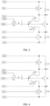
- the pixel driving circuit of the present application includes a first thin film transistor M1, a second thin film transistor M2, a third thin film transistor M3, a fourth thin film transistor M4, a fifth thin film transistor M5, a sixth thin film transistor M6, and a capacitor C.
- the first thin film transistor M1 and the second thin film transistor M2 are used to control the first light-emitting device D1 to emit light and to clear the charge of the first node A1.
- the third thin film transistor M3 is a data writing thin film transistor.
- the fourth thin film transistor M4 is the driving thin film transistor for both the first light-emitting device D1 and the second light-emitting device D2.
- the fifth thin film transistor M5 and the sixth thin film transistor M6 are used to control the second light-emitting device D2 to emit light and to clear the charge of the third node A3.
- the capacitor C may be a storage capacitor C.
- the first thin film transistor M1, the second thin film transistor M2, the third thin film transistor M3, the fourth thin film transistor M4, the fifth thin film transistor M5, and the sixth thin film transistor M6 may all be oxide semiconductor thin film transistors, low temperature polycrystalline silicon thin film transistors, or amorphous silicon thin film transistors, i.e., the types of thin film transistors T1 to T7 may all be Indium Gallium Zinc Oxide (IGZO), Low Temperature Poly-silicon (LTPS), or Amorphous Silicon (A-Si).
- IGZO Indium Gallium Zinc Oxide
- LTPS Low Temperature Poly-silicon
- A-Si Amorphous Silicon
- a controlled end of the first thin film transistor M1 is connected to a first control signal Ctr1, a first end of the first thin film transistor M1 is connected to a first supply voltage Vss1, and a second end of the first thin film transistor M1 is connected to a first node A1.
- a controlled end of the second thin film transistor M2 is connected to a second control signal Ctr2, a first end of the second thin film transistor M2 is connected to a fourth node A4 and a second end of the second thin film transistor M2 is connected to the second end of the first thin film transistor M1.
- a controlled end of the second thin film transistor M3 is connected to a scanning signal Scan, a first end of the second thin film transistor M3 is connected to a data signal Data and a second end of the second thin film transistor M3 is connected to a second node A2.
- a controlled end of the fourth thin film transistor M4 is connected to a fourth node A4, a first end of the fourth thin film transistor M4 is connected to the first node A1 and a second end of the fourth thin film transistor M4 is connected to a third node A3.
- a controlled end of the fifth thin film transistor M5 is connected to a third control signal Ctr3, a first end of the fifth thin film transistor M5 is connected to the fourth node A4 and a second end of the fifth thin film transistor M5 is connected to the third node A3.
- a controlled end of the sixth thin film transistor M6 is connected to the fourth control signal Ctr4, a first end of the sixth thin film transistor M6 is connected to the second end of the fifth thin film transistor M5, and a second end of the sixth thin film transistor M6 is connected to a second supply voltage Vss2.
- An end of the capacitor C is connected to the second node A2, and another end of the capacitor C is connected to the fourth node A4.
- An anode of the first light-emitting device D1 is connected to the first node A1, and a cathode of the first light-emitting device D1 is connected to the first supply voltage Vss1.
- the anode of the second light-emitting device D2 is connected to the third node A3, and the cathode of the second light-emitting device D2 is connected to the second supply voltage Vss2.
- a first reset stage T1 a first sampling stage T2, a first data writing stage T3, a first light-emitting stage T4, a second reset stage, a second sampling stage T6, a second data writing stage T7, and a second light-emitting stage T8, the scanning signal Scan, the first control signal Ctr1, the second control signal Ctr2, the third control signal Ctr3, the fourth control signal Ctr4, the first supply voltage Vss1, the second supply voltage Vss2 and the data signal Data are controlled to be at different potentials, so that the pixel driving circuit of the present application can drive the first light-emitting device D1 and the second light-emitting device D2 to emit light successively.
- the pixel driving circuit of the present application can be regarded as a 3T0.5C circuit structure.
- the first control signal Ctr1, the second control signal Ctr2, the third control signal Ctr3, the fourth control signal Ctr4, the scanning signal Scan and the data signal Data can be obtained from the output of an external timing controller, and the first supply voltage Vss1 and the second supply voltage Vss2 can be obtained from the output of an external common voltage generation circuit.
- the pixel driving circuit of the present application can make the first light-emitting device D1 and the second light-emitting device D2 to be in reverse bias state, to reduce the aging speed of the light-emitting device, which is conducive to extending the service life of the self-light-emitting display panel.
- the first control signal Ctr1, the second control signal Ctr2, the third control signal Ctr3, the fourth control signal Ctr4, the first supply voltage Vss1, the second supply voltage Vss2, the scanning signal Scan, and the data signal Data are combined to and applied successively to the first reset stage T1, the first sampling stage T2, the first data writing stage T3, the first light-emitting stage T4, the second reset stage T5, the second sampling stage T6, the second data writing stage T7, and the second light-emitting stage T8.
- the first light-emitting device D1 emits light in the first light-emitting stage T4, and the second light-emitting device D2 emits light in the second light-emitting stage T8.
- FIG. 1 may also be a schematic diagram of the pathway of the pixel driving circuit of the present application in the first reset stage T1 under the driving timing shown in FIG. 2 .
- the scanning signal Scan the first control signal Ctr1, the second control signal Ctr2, the third control signal Ctr3, the fourth control signal Ctr4, the first supply voltage Vss1, the second supply voltage Vss2, and the data signal Data are all at low potential to control the first thin film transistor M1, the second thin film transistor M2, the third thin film transistor M3, the fourth thin film transistor M4, the fifth thin film transistor M5, and the sixth thin film transistor M6 to be turned on.
- the data signal Data, the first supply voltage Vss1, and the second supply voltage Vss2 are at the low potential. It should be noted that the low potentials of the data signal Data, the first supply voltage Vss1, and the second supply voltage Vss2 in the present application are 0V, to clear the residual charge of the pixel driving circuit, to reset an terminal voltage of the capacitor C and the potential value of the controlled end of the fourth thin film transistor M4 to 0 quasi-loaction.
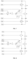
- FIG. 3 is a schematic diagram of the pathway of the pixel driving circuit of the present application in the first sampling stage T2 under the driving timing shown in FIG. 2 .
- the second control signal Ctr2 and the fourth control signal Ctr4 are both at the low potential to control the second thin film transistor M2 and the sixth thin film transistor M6 to turn on.
- the first control signal Ctr1, the scanning signal Scan, and the third control signal Ctr3 are all at the high potential to control the first thin film transistor M1, the third thin film transistor M3, and the fifth thin film transistor M5 to turn off.
- the potential value of the first node A1 is less than the high potential of the first supply voltage Vss1 at this time to make the first light-emitting device D1 be in the reverse bias state, to improve the aging process of the first light-emitting device D1.
- FIG. 4 is a schematic diagram of the pathway of the pixel driving circuit of the present application in the first data writing stage T3 under the driving timing shown in FIG. 2 .
- the second control signal Ctr2 is at the low potential to control the second thin film transistor M2 to turn on.
- the first control signal Ctr1, the third control signal Ctr3, and the fourth control signal Ctr4 are all at the high potential to control the first thin film transistor M1, the fifth thin film transistor M5, and the sixth thin film transistor M6 to turn off.
- the scanning signal Scan is at the low potential in the preset substage T31 to control the third thin film transistor M3 to turn on in the preset substage T31, and the scanning signal Scan is at the high potential in the first data writing stage T3 other than the preset substage T31 to control the third thin film transistor M3 to turn off outside the preset substage T31.
- a rising edge (a signal edge from low potential to high potential) of the scanning signal Scan (n) of the first light-emitting device D1 that emits light first at the end of its preset substage T31 corresponds to a rising edge of the scanning signal Scan (n+2) (a signal edge from high potential to low potential) of the light-emitting device that emits light later at the beginning of its preset substage T32.
- FIG. 5 is a schematic diagram of the pathway of the pixel driving circuit of the present application in the first light-emitting stage T4 under the driving timing shown in FIG. 2 .
- the fourth control signal Ctr4 is at the low potential to control the sixth thin film transistor M6 to turn on.
- the first control signal Ctr1, the second control signal Ctr2, the scanning signal Scan and the third control signal Ctr3 are all at the high potential to control the first thin film transistor M1, the second thin film transistor M2, the third thin film transistor M3 and the fifth thin film transistor M5 to turn off.
- the first supply voltage Vss1 is at negative potential
- the second supply voltage Vss2 is at the high potential
- the data signal Data is at the low potential.
- the negative potential of the first supply voltage Vss1 is less than its low potential, such that the potential of third node A3 can be pulled up to the high potential of the second supply voltage Vss2, and the fourth thin film transistor M4 is turned on to generate the current flowing through the first light-emitting device D1, to drive the first light-emitting device D1 to emit light
- the current flowing through the first light-emitting device D1 when the first light-emitting device D1 emits light is only related to the data signal Data, and is not related to the threshold voltage of the fourth thin film transistor M4, the first supply voltage Vss1 and second supply voltage Vss2, that is, it does not vary with the change in the threshold voltage of the fourth thin film transistor M4, the first supply voltage Vss1 and the second supply voltage Vss2, to eliminate the influence of the threshold voltage defect of the fourth thin film transistor M4 and the voltage drop of the supply voltage on the current flowing through the first light-emitting device D1.
- the data signal Data, the first supply voltage Vss1, and the second supply voltage Vss2 are at the low potential to clear the residual charge of the pixel driving circuit, to reset the terminal voltage of the capacitor C and the potential value of the controlled end of the fourth thin film transistor M4 to 0 quasi-location again.
- FIG. 6 is a schematic diagram of the pathway of the pixel driving circuit of the present application in the second sampling stage T6 under the driving timing shown in FIG. 2 .
- the first control signal Ctr1, the scanning signal Scan, and the third control signal Ctr3 are all at the low potential to control the first thin film transistor M1, the third thin film transistor M3, and the fifth thin film transistor M5 to turn on.
- the second control signal Ctr2 and the fourth control signal Ctr4 are both at the high potential to control the second thin film transistor M2 and the sixth thin film transistor M6 to turn off.
- the data signal Data is at the low potential
- the first supply voltage Vss1 and the second supply voltage Vss2 are at the high potential
- the terminal voltage of the capacitor C remains 0V due to the coupling effect of the capacitor C.
- , V S1 is a potential value of the first supply voltage Vss1.
- the potential value of the third node A3 is less than the high potential of the second supply voltage Vss2, to make the second light-emitting device D2 to be in the reverse bias state, to improve the aging process of the second light-emitting device D2.
- FIG. 7 is a schematic diagram of the pathway of the pixel driving circuit of the present application in the second data writing stage T7 under the driving timing shown in FIG. 2 .
- the third control signal Ctr3 is at the low potential to control the fifth thin film transistor M5 to turn on.
- the first control signal Ctr1, the second control signal Ctr2, and the fourth control signal Ctr4 are all at the high potential to control the first thin film transistor M1, the second thin film transistor M2, and the sixth thin film transistor M6 to turn off.
- a rising edge (a signal edge from the low potential to the high potential) of the scanning signal Scan (n+1) of the second light-emitting device D2 that emits light first at the end of its preset substage T71 corresponds to a rising edge of the scanning signal Scan (n+3) (a signal edge from the high potential to the low potential) of the light-emitting device that emits light later at the beginning of its preset substage T72.
- FIG. 8 is a schematic diagram of the pathway of the pixel driving circuit of the present application in the second light-emitting stage T8 under the driving timing shown in FIG. 2 .
- the first control signal Ctr1 is at the low potential to control the first thin film transistor M1 to turn on.
- the second control signal Ctr2, the fourth control signal Ctr4, the third control signal Ctr3 and the scanning signal Scan are all at the high potential to control the second thin film transistor M2, the sixth thin film transistor M6, the fifth thin film transistor M5 and the third thin film transistor M3 to turn off.
- the first supply voltage Vss1 is at the high potential
- the second supply voltage Vss2 is at the negative potential
- the data signal Data is at the low potential.
- the negative potential of the second supply voltage Vss2 is less than its low potential, such that the potential of the first node A1 can be pulled up to the high potential of the first supply voltage Vss1, and the fourth thin film transistor M4 is turned on to generate the current flowing through the second light-emitting device D2, to drive the second light-emitting device D2 to emit light
- the present application also provides a pixel driving method applied to a pixel driving circuit, the specific structure of which refers to the above first embodiment. Since the pixel driving method adopts all the technical solutions of the above first embodiment, thus it has at least all the beneficial effects brought about by the technical solutions of the above first embodiment, which will not be repeated here.
- the first control signal Ctr1, the second control signal Ctr2, the third control signal Ctr3, the fourth control signal Ctr4, the scanning signal Scan, and the data signal Data are combined and applied successively to the first reset stage T1, the first sampling stage T2, the first data writing stage T3, the first light-emitting stage T4, the second reset stage T5, the second sampling stage T6, the second data writing stage T7, and the second light-emitting stage T8.
Landscapes
- Engineering & Computer Science (AREA)
- Physics & Mathematics (AREA)
- Computer Hardware Design (AREA)
- General Physics & Mathematics (AREA)
- Theoretical Computer Science (AREA)
- Control Of Indicators Other Than Cathode Ray Tubes (AREA)
- Control Of El Displays (AREA)
- Electroluminescent Light Sources (AREA)
- Devices For Indicating Variable Information By Combining Individual Elements (AREA)
Abstract
Description
- This application claims priority to
Chinese Patent Application No. 202211359796.0, filed on November 2, 2022 - The present application relates to the technical field of pixel driving, and in particular to a pixel driving circuit, a pixel driving method and a display panel.
- Currently, for display panels that use light-emitting devices as pixels, each light-emitting device needs to be equipped with a pixel driving circuit, but each existing pixel driving circuit often requires six or more thin film transistors to compensate threshold voltages of the driving thin film transistors, thereby affecting a transmission rate of the display panel.
- The main objective of the present application is to provide a pixel driving circuit, which aims to solve a problem that a transmission rate of the self-light-emitting display panel is lower.
- In order to achieve the above objective, the present application provides a pixel driving circuit, applied to a display panel provided with a pixel array. The pixel array includes a first light-emitting device and a second light-emitting device adjacent to each other and located on a same column;
- an anode of the first light-emitting device is connected to a first node and a cathode of the first light-emitting device is connected to a first supply voltage;
- an anode of the second light-emitting device is connected to a third node and a cathode of the second light-emitting device is connected to a second supply voltage;
- the pixel driving circuit includes a first thin film transistor, a second thin film transistor, a third thin film transistor, a fourth thin film transistor, a fifth thin film transistor, a sixth thin film transistor and a capacitor;
- a controlled end of the first thin film transistor is connected to a first control signal, a first end of the first thin film transistor is connected to the first supply voltage and a second end of the first thin film transistor is connected to the first node;
- a controlled end of the second thin film transistor is connected to a second control signal, a first end of the second thin film transistor is connected to a fourth node and a second end of the second thin film transistor is connected to the second end of the first thin film transistor;
- a controlled end of the third thin film transistor is connected to a scanning signal, a first end of the third thin film transistor is connected to a data signal and a second end of the third thin film transistor is connected to a second node;
- a controlled end of the fourth thin film transistor is connected to the fourth node, a first end of the fourth thin film transistor is connected to the first node and a second end of the fourth thin film transistor is connected to a third node;
- a controlled end of the fifth thin film transistor is connected to a third control signal, a first end of the fifth thin film transistor is connected to the fourth node and a second end of the fifth thin film transistor is connected to the third node;
- a controlled end of the sixth thin film transistor is connected to a fourth control signal, a first end of the sixth thin film transistor is connected to the second end of the fifth thin film transistor, a second end of the sixth thin film transistor is connected to the second supply voltage; and
- an end of the capacitor is connected to the second node and another end of the capacitor is connected to the fourth node.
- The present application also provides a pixel driving method, applied to the pixel driving circuit as mentioned above, including:
- in a first reset stage, controlling the first thin film transistor, the second thin film transistor, the third thin film transistor, the fourth thin film transistor, the fifth thin film transistor, and the sixth thin film transistor to turn on, and controlling the data signal, the first supply voltage, and the second supply voltage to be at low potential;
- in a first sampling stage, controlling the second thin film transistor and the sixth thin film transistor to turn on, and controlling the first thin film transistor, the third thin film transistor, and the fifth thin film transistor to turn off, and controlling the data signal to be at the low potential, the first supply voltage and the second supply voltage to be at high potential, to make a potential of the fourth node to be a difference between absolute values of the second supply voltage and a threshold voltage of the fourth thin film transistor;
- in a first data writing stage, controlling the second thin film transistor to turn on, and controlling the first thin film transistor, the fifth thin film transistor, and the sixth thin film transistor to turn off, and controlling the third thin film transistor to turn on in a preset substage, and controlling the third thin film transistor to turn off outside the preset substage, and controlling the data signal, the first supply voltage and the second supply voltage to be at the high potential, to make the potential of the fourth node to be a sum of the difference between the absolute values of the second supply voltage and the threshold voltage of the fourth thin film transistor and the data signal;
- in a first light-emitting stage, controlling the sixth thin film transistor to turn on, and controlling the first thin film transistor, the second thin film transistor, the third thin film transistor and the fifth thin film transistor to turn off, and controlling the first supply voltage to be at negative potential, and controlling the second supply voltage to be at the high potential, and controlling the data signal to be at the low potential, to make the first light-emitting device to emit light;
- in a second reset stage, controlling the first thin film transistor, the second thin film transistor, the third thin film transistor, the fourth thin film transistor, the fifth thin film transistor and the sixth thin film transistor to turn on, and controlling the data signal, the first supply voltage and the second supply voltage to be at the low potential;
- in a second sampling stage, controlling the first thin film transistor, the third thin film transistor, the fifth thin film transistor to turn on, and controlling the second thin film transistor and the sixth thin film transistor to turn off, and controlling the data signal to be at the low potential, and controlling the first supply voltage and the second supply voltage to be at the high potential, to make the potential of the fourth node to be a difference between absolute values of the first supply voltage and the threshold voltage of the fourth thin film transistor;
- in a second data writing stage, controlling the fifth thin film transistor to turn on, and controlling the first thin film transistor, the second thin film transistor and the sixth thin film transistor to turn off, and controlling the third thin film transistor to turn on in the preset substage, and controlling the third thin film transistor to turn off outside the preset substage, and controlling the data signal, the first supply voltage and the second supply voltage to be at the high potential, to make the potential of the fourth node to be a sum of the difference between the absolute values of the first supply voltage and the threshold voltage of the fourth thin film transistor and the data signal; and
- in a second light-emitting stage, controlling the first thin film transistor to turn on, and controlling the second thin film transistor, the third thin film transistor, the fifth thin film transistor and the sixth thin film transistor to turn off, and controlling the first supply voltage to be at the high potential, and controlling the second supply voltage to be at the negative potential, and controlling the data signal to be at the low potential, to make the second light-emitting device to emit light.
- The present application also provides a display panel, including:
- a pixel array including a first light-emitting device and a second light-emitting device adjacent to each other and located on a same column; and
- the pixel driving circuit as mentioned above, the pixel driving circuit being connected to the first light-emitting device and the second light-emitting device.
- The technical solution of the present application adopts the first thin film transistor, the second thin film transistor, the third thin film transistor, the fourth thin film transistor, the fifth thin film transistor, the sixth thin film transistor and the capacitor to form a pixel driving circuit of 3T0.5C circuit structure, so that two adjacent light-emitting devices on the same column can share a pixel driving circuit, and the threshold voltage of the driving thin film transistor and a voltage drop of the supply voltage can be compensated, thus the influence of the threshold voltage defect of the driving thin film transistor and the voltage drop of the supply voltage on the current flowing through the light-emitting device can be eliminated, to improve the display uniformity of the self-light-emitting display panel. Compared with at least 12 thin film transistors required for two separate pixel driving circuits, the number of thin film transistors is greatly reduced, to greatly improve the transmission rate of the panel. In addition, the pixel driving circuit of the present application can make the first light-emitting device and the second light-emitting device to be in reverse bias state, to reduce the aging speed of the light-emitting device, which is conducive to increasing the service life of the self-light-emitting display panel.
- In order to more clearly illustrate the technical solutions in the embodiments of the present application or related art, the following is a brief description of the drawings for the description of the embodiments or related art, it is obvious that the drawings in the following description are only some of the embodiments of the present application, other structures can be obtained by those skilled in the art according to structures in these drawings without creative works.
-
FIG. 1 is a schematic diagram of a pixel driving circuit according to a first embodiment of the present application. -
FIG. 2 is a schematic diagram of a timing of the pixel driving circuit according to the first embodiment of the present application. -
FIG. 3 is a schematic diagram of a pathway of the pixel driving circuit in a first sampling stage according to the first embodiment of the present application. -
FIG. 4 is a schematic diagram of the pathway of the pixel driving circuit in a first data stage according to the first embodiment of the present application. -
FIG. 5 is a schematic diagram of the pathway of the pixel driving circuit in a first light-emitting writing stage according to the first embodiment of the present application. -
FIG. 6 is a schematic diagram of the pathway of the pixel driving circuit in a second sampling stage according to the first embodiment of the present application. -
FIG. 7 is a schematic diagram of the pathway of the pixel driving circuit in a second data stage according to the first embodiment of the present application. -
FIG. 8 is a schematic diagram of the pathway of the pixel driving circuit in a second light-emitting stage according to the first embodiment of the present application. -
FIG. 9 is a flowchart of a pixel driving method according to a second embodiment of the present application. - The realization of the purpose, functional features and advantages of the present application will be further illustrated with reference to the drawings in conjunction with the embodiments.
- The technical solutions in the embodiments of the present application will be clearly and completely described below in conjunction with the drawings in the embodiments of the present application, and it is clear that the described embodiments are only some of the embodiments of the present application, and not all of them. Based on the embodiments in the present application, all other embodiments obtained by those skilled in the art fall within the scope of the present application without creative labor.
- In addition, the descriptions such as "first" and "second" in the present application are for descriptive purposes only and are not to be construed as indicating or implying their relative importance or implicitly specifying the number of technical features indicated. Thus, the features defined with "first" and "second" may explicitly or implicitly include at least one such feature. In addition, the technical solutions of each embodiment can be combined with each other, but only on the basis that they can be achieved by those skilled in the art, when the combination of technical solutions appear to contradict each other or can not be achieved, it should be considered that this combination of technical solutions does not exist, and is not within the scope of the present application.
- The present application provides a pixel driving circuit that can be applied to a display panel.
- The display panel may include a pixel layer, a light-emitting layer, a driving circuit layer and an array substrate arranged in sequence. The driving circuit layer is provided on the array substrate. The pixel layer may include a plurality of pixels arranged in an array, and the light-emitting layer is provided with a light-emitting device for each pixel. The driving circuit layer may include a plurality of pixel driving circuits, each pixel driving circuit is connected to a light-emitting device, and each pixel driving circuit is used to drive the light-emitting device of the corresponding pixel to emit light, to realize the self-light-emitting display of the display panel. Light-emitting devices can be organic light-emitting diodes (OLED), mini-LEDs or micro-LEDs, without limitation here. The embodiment of the present application takes that light-emitting devices are organic light-emitting diodes as an example to illustrate.
- In practical applications, the pixel driving circuit may be provided with a driving thin film transistor for controlling the flow of current through the light-emitting device, and the threshold voltage of the driving thin film transistor has a nonuniformity problem, and the threshold voltage will also drift with an increase of operating time to cause the display panel to produce uneven brightness cloud patterns. In order to solve above defects of the threshold voltage, the existing technology usually increases the number of thin film transistors and increases the storage capacitor C, resulting in that the number of thin film transistors in each pixel driving circuit is 6 or more, and it can be noted from the location of the driving circuit layer where the pixel driving circuit is located in in the display panel that the more the number of thin film transistors in each pixel driving circuit, the less light from the light-emitting layer passing through the driving circuit layer, and the lower the transmission rate of the display panel. Secondly, the pixel driving circuit also needs to access the supply voltage to drive the corresponding light-emitting devices, the power supply line itself has a certain degree of internal resistance, so that the actual supply voltage delivered to the light-emitting devices has a voltage drop, and because the voltage drops of the supply voltages of different display devices are different, which will lead to uneven luminance of the light-emitting devices and a faster aging speed of the light-emitting devices in the pixel driving circuit due to being in the forward bias state, to cause a lower service life of the self-light-emitting display panel.
- In view of the above problems, the present application provides a pixel driving circuit for driving two light-emitting devices adjacent to each other and located on a same column in a pixel array, the first light-emitting device D1 may be a light-emitting device on an odd number of rows and the second light-emitting device D2 may be a light-emitting device on an even number of rows.
- Referring to
FIG. 1 , the pixel driving circuit of the present application includes a first thin film transistor M1, a second thin film transistor M2, a third thin film transistor M3, a fourth thin film transistor M4, a fifth thin film transistor M5, a sixth thin film transistor M6, and a capacitor C. The first thin film transistor M1 and the second thin film transistor M2 are used to control the first light-emitting device D1 to emit light and to clear the charge of the first node A1. The third thin film transistor M3 is a data writing thin film transistor. The fourth thin film transistor M4 is the driving thin film transistor for both the first light-emitting device D1 and the second light-emitting device D2. The fifth thin film transistor M5 and the sixth thin film transistor M6 are used to control the second light-emitting device D2 to emit light and to clear the charge of the third node A3. The capacitor C may be a storage capacitor C. The first thin film transistor M1, the second thin film transistor M2, the third thin film transistor M3, the fourth thin film transistor M4, the fifth thin film transistor M5, and the sixth thin film transistor M6 may all be oxide semiconductor thin film transistors, low temperature polycrystalline silicon thin film transistors, or amorphous silicon thin film transistors, i.e., the types of thin film transistors T1 to T7 may all be Indium Gallium Zinc Oxide (IGZO), Low Temperature Poly-silicon (LTPS), or Amorphous Silicon (A-Si). Of course, the thin film transistors M1 to M6 can adopts different types of thin film transistors, respectively, their combination are various, which will not be described here. In the embodiment, the first thin film transistor M1, the second thin film transistor M2, the third thin film transistor M3, the fourth thin film transistor M4, the fifth thin film transistor M5, and the sixth thin film transistor M6 can be P-type thin film transistors. It is understood that a controlled end of the thin film transistor may be a gate, one of the first end and the second end of the thin film transistor may be a source, and the other of the first end and the second end of the thin film transistor may be a drain. The first end and the second end of the thin film transistor can be connected when the thin film transistor is turned on, and the first end and the second end of the thin film transistor can be disconnected when the thin film transistor is turned off. - A controlled end of the first thin film transistor M1 is connected to a first control signal Ctr1, a first end of the first thin film transistor M1 is connected to a first supply voltage Vss1, and a second end of the first thin film transistor M1 is connected to a first node A1.
- A controlled end of the second thin film transistor M2 is connected to a second control signal Ctr2, a first end of the second thin film transistor M2 is connected to a fourth node A4 and a second end of the second thin film transistor M2 is connected to the second end of the first thin film transistor M1.
- A controlled end of the second thin film transistor M3 is connected to a scanning signal Scan, a first end of the second thin film transistor M3 is connected to a data signal Data and a second end of the second thin film transistor M3 is connected to a second node A2.
- A controlled end of the fourth thin film transistor M4 is connected to a fourth node A4, a first end of the fourth thin film transistor M4 is connected to the first node A1 and a second end of the fourth thin film transistor M4 is connected to a third node A3.
- A controlled end of the fifth thin film transistor M5 is connected to a third control signal Ctr3, a first end of the fifth thin film transistor M5 is connected to the fourth node A4 and a second end of the fifth thin film transistor M5 is connected to the third node A3.
- A controlled end of the sixth thin film transistor M6 is connected to the fourth control signal Ctr4, a first end of the sixth thin film transistor M6 is connected to the second end of the fifth thin film transistor M5, and a second end of the sixth thin film transistor M6 is connected to a second supply voltage Vss2.
- An end of the capacitor C is connected to the second node A2, and another end of the capacitor C is connected to the fourth node A4.
- An anode of the first light-emitting device D1 is connected to the first node A1, and a cathode of the first light-emitting device D1 is connected to the first supply voltage Vss1. The anode of the second light-emitting device D2 is connected to the third node A3, and the cathode of the second light-emitting device D2 is connected to the second supply voltage Vss2.
- In a first reset stage T1, a first sampling stage T2, a first data writing stage T3, a first light-emitting stage T4, a second reset stage, a second sampling stage T6, a second data writing stage T7, and a second light-emitting stage T8, the scanning signal Scan, the first control signal Ctr1, the second control signal Ctr2, the third control signal Ctr3, the fourth control signal Ctr4, the first supply voltage Vss1, the second supply voltage Vss2 and the data signal Data are controlled to be at different potentials, so that the pixel driving circuit of the present application can drive the first light-emitting device D1 and the second light-emitting device D2 to emit light successively. In other words, the pixel driving circuit of the present application can be regarded as a 3T0.5C circuit structure.
- It should be noted that the first control signal Ctr1, the second control signal Ctr2, the third control signal Ctr3, the fourth control signal Ctr4, the scanning signal Scan and the data signal Data can be obtained from the output of an external timing controller, and the first supply voltage Vss1 and the second supply voltage Vss2 can be obtained from the output of an external common voltage generation circuit.
- In this way, two adjacent light-emitting devices on the same column can share a pixel driving circuit, and the threshold voltage of the fourth thin film transistor M4 and a voltage drop of the supply voltage can be compensated, thus the influence of the threshold voltage defect of the driving thin film transistor and the voltage drop of the supply voltage on the current flowing through the light-emitting device can be eliminated, to improve the display uniformity of the self-light-emitting display panel. Compared with at least 12 thin film transistors required for two separate pixel driving circuits, the number of thin film transistors is greatly reduced, to greatly improve the transmission rate of the panel. In addition, the pixel driving circuit of the present application can make the first light-emitting device D1 and the second light-emitting device D2 to be in reverse bias state, to reduce the aging speed of the light-emitting device, which is conducive to extending the service life of the self-light-emitting display panel.
- In an embodiment, the first control signal Ctr1, the second control signal Ctr2, the third control signal Ctr3, the fourth control signal Ctr4, the first supply voltage Vss1, the second supply voltage Vss2, the scanning signal Scan, and the data signal Data are combined to and applied successively to the first reset stage T1, the first sampling stage T2, the first data writing stage T3, the first light-emitting stage T4, the second reset stage T5, the second sampling stage T6, the second data writing stage T7, and the second light-emitting stage T8. The first light-emitting device D1 emits light in the first light-emitting stage T4, and the second light-emitting device D2 emits light in the second light-emitting stage T8.
- Referring to
FIGS. 1 and 2, FIG. 1 may also be a schematic diagram of the pathway of the pixel driving circuit of the present application in the first reset stage T1 under the driving timing shown inFIG. 2 . In the first reset stage T1, the scanning signal Scan, the first control signal Ctr1, the second control signal Ctr2, the third control signal Ctr3, the fourth control signal Ctr4, the first supply voltage Vss1, the second supply voltage Vss2, and the data signal Data are all at low potential to control the first thin film transistor M1, the second thin film transistor M2, the third thin film transistor M3, the fourth thin film transistor M4, the fifth thin film transistor M5, and the sixth thin film transistor M6 to be turned on. At this time, the data signal Data, the first supply voltage Vss1, and the second supply voltage Vss2 are at the low potential. It should be noted that the low potentials of the data signal Data, the first supply voltage Vss1, and the second supply voltage Vss2 in the present application are 0V, to clear the residual charge of the pixel driving circuit, to reset an terminal voltage of the capacitor C and the potential value of the controlled end of the fourth thin film transistor M4 to 0 quasi-loaction. - Referring to
FIGS. 1, 2 and3, FIG. 3 is a schematic diagram of the pathway of the pixel driving circuit of the present application in the first sampling stage T2 under the driving timing shown inFIG. 2 . In the first sampling stage T2, the second control signal Ctr2 and the fourth control signal Ctr4 are both at the low potential to control the second thin film transistor M2 and the sixth thin film transistor M6 to turn on. The first control signal Ctr1, the scanning signal Scan, and the third control signal Ctr3 are all at the high potential to control the first thin film transistor M1, the third thin film transistor M3, and the fifth thin film transistor M5 to turn off. At this time, the data signal Data is at the low potential, the first supply voltage Vss1 and the second supply voltage Vss2 are at the high potential, and the terminal voltage of capacitor C remains 0V due to the coupling effect of capacitor C. The potential of the controlled end of the fourth thin film transistor M4, i.e., the potential of the fourth node A4, can be charged to the difference between absolute values of the second supply voltage Vss2 and the threshold voltage of the fourth thin film transistor M4, which is expressed by the formula VG=VS2-|VTH|, VG is a potential value of the controlled end of the fourth thin film transistor M4, VS2 is a potential value of the second supply voltage Vss2, and VTH is the threshold voltage of the fourth thin film transistor M4. Secondly, the potential value of the first node A1 is less than the high potential of the first supply voltage Vss1 at this time to make the first light-emitting device D1 be in the reverse bias state, to improve the aging process of the first light-emitting device D1. - Referring to
FIG. 1, FIG. 2 andFIG. 4, FIG. 4 is a schematic diagram of the pathway of the pixel driving circuit of the present application in the first data writing stage T3 under the driving timing shown inFIG. 2 . In the first data writing stage T3, the second control signal Ctr2 is at the low potential to control the second thin film transistor M2 to turn on. The first control signal Ctr1, the third control signal Ctr3, and the fourth control signal Ctr4 are all at the high potential to control the first thin film transistor M1, the fifth thin film transistor M5, and the sixth thin film transistor M6 to turn off. The scanning signal Scan is at the low potential in the preset substage T31 to control the third thin film transistor M3 to turn on in the preset substage T31, and the scanning signal Scan is at the high potential in the first data writing stage T3 other than the preset substage T31 to control the third thin film transistor M3 to turn off outside the preset substage T31. At this time, the data signal Data, the first supply voltage Vss1 and the second supply voltage Vss2 are all at the high potential, so that the data signal Data is written to the second node A2 via the third thin film transistor M3, and the potential of the fourth node A4 is a sum of a difference between absolute values of the second supply voltage Vss2 and the threshold voltage of the fourth thin film transistor M4 and the data signal Data, which is expressed by the formula VG= VS2-|VTH|+VDATA, VDATA is the potential of data signal Data. It should be noted that, for the closest two first light-emitting devices D1 on the same column, a rising edge (a signal edge from low potential to high potential) of the scanning signal Scan (n) of the first light-emitting device D1 that emits light first at the end of its preset substage T31 corresponds to a rising edge of the scanning signal Scan (n+2) (a signal edge from high potential to low potential) of the light-emitting device that emits light later at the beginning of its preset substage T32. - Referring to
FIG. 1, FIG. 2 andFIG. 5, FIG. 5 is a schematic diagram of the pathway of the pixel driving circuit of the present application in the first light-emitting stage T4 under the driving timing shown inFIG. 2 . In the first light-emitting stage T4, the fourth control signal Ctr4 is at the low potential to control the sixth thin film transistor M6 to turn on. The first control signal Ctr1, the second control signal Ctr2, the scanning signal Scan and the third control signal Ctr3 are all at the high potential to control the first thin film transistor M1, the second thin film transistor M2, the third thin film transistor M3 and the fifth thin film transistor M5 to turn off. At this time, the first supply voltage Vss1 is at negative potential, the second supply voltage Vss2 is at the high potential, and the data signal Data is at the low potential. It should be noted that the negative potential of the first supply voltage Vss1 is less than its low potential, such that the potential of third node A3 can be pulled up to the high potential of the second supply voltage Vss2, and the fourth thin film transistor M4 is turned on to generate the current flowing through the first light-emitting device D1, to drive the first light-emitting device D1 to emit light, the current flowing through the first light-emitting device D1 can be expressed by
- Referring to
FIGS. 1 and 2, FIG. 1 may also be a schematic diagram of the pathway of the pixel driving circuit of the present application in the second light-emitting stage T8 under the driving timing shown inFIG. 2 . In the second reset stage T5, the scanning signal Scan, the first control signal Ctr1, the second control signal Ctr2, the third control signal Ctr3, the fourth control signal Ctr4, the first supply voltage Vss1, the second supply voltage Vss2, and the data signal Data are all at the low potential to control the first thin film transistor M1, the second thin film transistor M2, the third thin film transistor M3, the fourth thin film transistor M4, the fifth thin film transistor M5, and the sixth thin film transistor M6 to turn on. At this time, the data signal Data, the first supply voltage Vss1, and the second supply voltage Vss2 are at the low potential to clear the residual charge of the pixel driving circuit, to reset the terminal voltage of the capacitor C and the potential value of the controlled end of the fourth thin film transistor M4 to 0 quasi-location again. - Referring to
FIGS. 1, 2 and6, FIG. 6 is a schematic diagram of the pathway of the pixel driving circuit of the present application in the second sampling stage T6 under the driving timing shown inFIG. 2 . In the second sampling stage T6, the first control signal Ctr1, the scanning signal Scan, and the third control signal Ctr3 are all at the low potential to control the first thin film transistor M1, the third thin film transistor M3, and the fifth thin film transistor M5 to turn on. The second control signal Ctr2 and the fourth control signal Ctr4 are both at the high potential to control the second thin film transistor M2 and the sixth thin film transistor M6 to turn off. At this time, the data signal Data is at the low potential, the first supply voltage Vss1 and the second supply voltage Vss2 are at the high potential, and the terminal voltage of the capacitor C remains 0V due to the coupling effect of the capacitor C. The potential of the controlled end of the fourth thin film transistor M4, i.e., the potential of the fourth node A4, can be charged to the difference between absolute values of the first supply voltage Vss1 and the threshold voltage of the fourth thin film transistor M4, which is expressed by the formula VG=VS1-|VTH|, VS1 is a potential value of the first supply voltage Vss1. Secondly, the potential value of the third node A3 is less than the high potential of the second supply voltage Vss2, to make the second light-emitting device D2 to be in the reverse bias state, to improve the aging process of the second light-emitting device D2. - Referring to
FIGS. 1, 2 and7, FIG. 7 is a schematic diagram of the pathway of the pixel driving circuit of the present application in the second data writing stage T7 under the driving timing shown inFIG. 2 . In the second data writing stage T7, the third control signal Ctr3 is at the low potential to control the fifth thin film transistor M5 to turn on. The first control signal Ctr1, the second control signal Ctr2, and the fourth control signal Ctr4 are all at the high potential to control the first thin film transistor M1, the second thin film transistor M2, and the sixth thin film transistor M6 to turn off. The scanning signal Scan is at the low potential in the preset substage T71 to control the third thin film transistor M3 to turn on in the preset substage T71, and the scanning signal Scan is at the high potential in the first data writing stage T3 other than the preset substage T71 to control the third thin film transistor M3 to turn off outside the preset substage T71. At this time, the data signal Data, the first supply voltage Vss1 and the second supply voltage Vss2 are all at the high potential, so that the data signal Data is written to the second node A2 via the third thin film transistor M3, and due to the coupling effect of the capacitor C, the potential of the fourth node A4 is a sum of the difference between absolute values of the first supply voltage Vss1 and the threshold voltage of the fourth thin film transistor M4 and the data signal Data, which is expressed by the formula VG= VS1-|VTH|+VDATA. It should be noted that for the closest two second light-emitting devices D2 on the same column, a rising edge (a signal edge from the low potential to the high potential) of the scanning signal Scan (n+1) of the second light-emitting device D2 that emits light first at the end of its preset substage T71 corresponds to a rising edge of the scanning signal Scan (n+3) (a signal edge from the high potential to the low potential) of the light-emitting device that emits light later at the beginning of its preset substage T72. - Referring to
FIG. 1, FIG. 2 andFIG. 8, FIG. 8 is a schematic diagram of the pathway of the pixel driving circuit of the present application in the second light-emitting stage T8 under the driving timing shown inFIG. 2 . In the second light-emitting stage T8, the first control signal Ctr1 is at the low potential to control the first thin film transistor M1 to turn on. The second control signal Ctr2, the fourth control signal Ctr4, the third control signal Ctr3 and the scanning signal Scan are all at the high potential to control the second thin film transistor M2, the sixth thin film transistor M6, the fifth thin film transistor M5 and the third thin film transistor M3 to turn off. At this time, the first supply voltage Vss1 is at the high potential, the second supply voltage Vss2 is at the negative potential, and the data signal Data is at the low potential. It should be noted that the negative potential of the second supply voltage Vss2 is less than its low potential, such that the potential of the first node A1 can be pulled up to the high potential of the first supply voltage Vss1, and the fourth thin film transistor M4 is turned on to generate the current flowing through the second light-emitting device D2, to drive the second light-emitting device D2 to emit light, the current flowing through the second light-emitting device D2 can be expressed by
- It can be seen that the current flowing through the second light-emitting device D2 light when the second light-emitting device D2 emits light is also only related to the data signal Data, and not related to the threshold voltage of the fourth thin film transistor M4, the first supply voltage Vss1 and the second supply voltage Vss2, that is, it does not vary with the change in the threshold voltage of the fourth thin film transistor M4, the first supply voltage Vss1 and the second supply voltage Vss2, to eliminate the influence of the threshold voltage defect of the fourth thin film transistor M4 and the voltage drop of the supply voltage on the current flowing through the second light-emitting device D2.
- Referring to
FIG. 9 , the present application also provides a pixel driving method applied to a pixel driving circuit, the specific structure of which refers to the above first embodiment. Since the pixel driving method adopts all the technical solutions of the above first embodiment, thus it has at least all the beneficial effects brought about by the technical solutions of the above first embodiment, which will not be repeated here. - The first control signal Ctr1, the second control signal Ctr2, the third control signal Ctr3, the fourth control signal Ctr4, the scanning signal Scan, and the data signal Data are combined and applied successively to the first reset stage T1, the first sampling stage T2, the first data writing stage T3, the first light-emitting stage T4, the second reset stage T5, the second sampling stage T6, the second data writing stage T7, and the second light-emitting stage T8.
- The pixel driving method includes:
- Step S1, in the first reset stage T1, controlling the first thin film transistor M1, the second thin film transistor M2, the third thin film transistor M3, the fourth thin film transistor M4, the fifth thin film transistor M5, and the sixth thin film transistor M6 to turn on, and controlling the data signal Data, the first supply voltage Vss1 and the second supply voltage Vss2 to be at low potential. In this stage, the scanning signal Scan, the first control signal Ctr1, the second control signal Ctr2, the third control signal Ctr3, the fourth control signal Ctr4, the first supply voltage Vss1, the second supply voltage Vss2, and the data signal Data are all at the low potential, so that the pixel driving circuit can clear the residual charge to reset the terminal voltage of the capacitor C and the potential value of the controlled end of the fourth thin film transistor M4 to 0 quasi-location.
- Step S2, in the first sampling stage T2, controlling the second thin film transistor M2 and the sixth thin film transistor M6 to turn on, and controlling the first thin film transistor M1, the third thin film transistor M3, and the fifth thin film transistor M5 to turn off, and controlling the data signal Data to be at low potential and the first supply voltage Vss1 and the second supply voltage Vss2 to be at high potential, to make the potential of the fourth node A4 to be a difference between absolute values of the second supply voltage Vss2 and the threshold voltage of the fourth thin film transistor M4. In this stage, the second control signal Ctr2 and the fourth control signal Ctr4 are at the low potential; the first control signal Ctr1, the scanning signal Scan, and the third control signal Ctr3 are at the high potential, such that the potential of the controlled end of the fourth thin film transistor M4, i.e., the potential of the fourth node A4, can be charged to the difference between the absolute values of the second supply voltage Vss2 and the threshold voltage of the fourth thin film transistor M4, which is expressed by the formula VG=VS2-|VTH|, and at this time the potential value of the first node A1 is less than the high potential of the first supply voltage Vss1, to make the first light-emitting device D1 to be in the reverse bias state, to improve the aging process of the first light-emitting device D1.
- Step S3, in the first data writing stage T3, controlling the second thin film transistor M2 to turn on, and controlling the first thin film transistor M1, the fifth thin film transistor M5 and the sixth thin film transistor M6 to turn off, and controlling the third thin film transistor M3 to turn on in the preset substage T31, and controlling the third thin film transistor M3 to turn off outside the preset substage T31, and controlling the data signal Data, the first supply voltage Vss1, and the second supply voltage Vss2 to be at the high potential, to make the potential of the fourth node A4 to be a sum of the difference between the absolute values of the second supply voltage Vss2 and the threshold voltage of the fourth thin film transistor M4 and the data signal Data. In this stage, the second control signal Ctr2 is at the low potential; the first control signal Ctr1, the third control signal Ctr3, and the fourth control signal Ctr4 are all at the high potential, and the scanning signal Scan is at the low potential in the preset substage T31 and at the high potential in the first data writing stage T3 other than the preset substage T31, so that the data signal Data can be written to the second node A2 via the third thin film transistor M3, and due to the coupling effect of the capacitor C, the potential of the fourth node A4 is the sum of the difference between the absolute values of the second supply voltage Vss2 and the threshold voltage of the fourth thin film transistor M4 and the data signal Data, which is expressed by the formula VG= VS2-|VTH|+VDATA.
- Step S4, in the first light-emitting stage T4, controlling the sixth thin film transistor M6 to turn on, and controlling the first thin film transistor M1, the second thin film transistor M2, the third thin film transistor M3 and the fifth thin film transistor M5 to turn off, and controlling the first supply voltage Vss1 to be at negative potential, and controlling the second supply voltage Vss2 to be at high potential, and controlling the data signal Data to be at the low potential to make the first light-emitting device D1 to emit light. In this stage, the fourth control signal Ctr4 is at the low potential, and the first control signal Ctr1, the second control signal Ctr2, the scanning signal Scan and the third control signal Ctr3 are all at the high potential, so that the potential of the third node A3 can be pulled up to the high potential of the second supply voltage Vss2, and the fourth thin film transistor M4 is turned on to generate the current flowing through the first light-emitting device D1, to drive the first light-emitting device D1 to emit light. In addition, as can be seen from the expression of the current flowing through the first light-emitting device D1, the current flowing through the first light-emitting device D1 when the first light-emitting device D1 emits light is only related to the data signal Data and is not related to the threshold voltage of the fourth thin film transistor M4, the first supply voltage Vss1 and the second supply voltage Vss2, i.e., it does not vary with change in the threshold voltage of the fourth thin film transistor M4, the first supply voltage Vss1 and the second supply voltage Vss2, to eliminate the influence of the threshold voltage defect of the fourth thin film transistor M4 and the voltage drop of the supply voltage on the current flowing through the first light-emitting device D1.
- Step S5, in a second reset stage T5, controlling the first thin film transistor M1, the second thin film transistor M2, the third thin film transistor M3, the fourth thin film transistor M4, the fifth thin film transistor M5, and the sixth thin film transistor M6 to turn on, and controlling the data signal Data, the first supply voltage Vss1, and the second supply voltage Vss2 to be at the low potential. In this stage, the scanning signal Scan, the first control signal Ctr1, the second control signal Ctr2, the third control signal Ctr3, the fourth control signal Ctr4, the first supply voltage Vss1, the second supply voltage Vss2 and the data signal Data are all at the low potential, so that the pixel driving circuit clears the residual charge to reset the terminal voltage of capacitor C and the potential value of the controlled end of the fourth thin film transistor M4 to the 0 quasi-location again.
- Step S6, in the second sampling stage T6, controlling the first thin film transistor M1, the third thin film transistor M3, and the fifth thin film transistor M5 to turn on, and controlling the second thin film transistor M2 and the sixth thin film transistor M6 to turn off, and controlling the data signal Data to be at the low potential, and controlling the first supply voltage Vss1 and the second supply voltage Vss2 to be at the high potential, to make potential of the fourth node A4 to be the difference between the absolute values of the first supply voltage Vss1 and the threshold voltage of the fourth thin film transistor M4. In this stage, the first control signal Ctr1, the scanning signal Scan, and the third control signal Ctr3 are at the low potential, and the second control signal Ctr2 and the fourth control signal Ctr4 are at the high potential, so that the potential of the controlled end of the fourth thin film transistor M4, i.e., the potential of the fourth node A4, can be charged to the difference between the absolute values of the first supply voltage Vss1 and the threshold voltage of the fourth thin film transistor M4, which is expressed by the formula VG=VS1-|VTH|, and the potential value of the third node A3 is less than the high potential of the second supply voltage Vss2 at this time, to make the second light-emitting device D2 to be in the reverse bias state, to improve the aging process of the second light-emitting device D2.
- Step S7, in the second data writing stage T7, controlling the fifth thin film transistor M5 to turn on, and controlling the first thin film transistor M1, the second thin film transistor M2 and the sixth thin film transistor M6 to turn off, and controlling the third thin film transistor M3 to turn on in the preset substage T71, and controlling the third thin film transistor M3 to turn off outside the preset substage T71, and controlling the data signal Data, the first supply voltage Vss1, and the second supply voltage Vss2 to be at the high potential, to make the potential of the fourth node A4 to be the sum of the difference between the absolute values of the first supply voltage Vss1 and the threshold voltage of the fourth thin film transistor M4 and the data signal Data. In this stage, the third control signal Ctr3 is at the low potential, the first control signal Ctr1, the second control signal Ctr2, and the fourth control signal Ctr4 are all at the high potential, and the scanning signal Scan is at the low potential in the preset substage T71 and at the high potential in the first data writing stage T3 other than the preset substage T71, such that the data signal Data is written to the second node A2 via the third thin film transistor M3, and due to the coupling effect of the capacitor C, the potential of the fourth node A4 is the sum of the difference between the absolute values of the first supply voltage Vss1 and the threshold voltage of the fourth thin film transistor M4 and the data signal Data, which is expressed by the formula VG= VS1-|VTH|+VDATA.
- Step S8, in the second light-emitting stage T8, controlling the first thin film transistor M1 to turn on, and controlling the second thin film transistor M2, the third thin film transistor M3, the fifth thin film transistor M5 and the sixth thin film transistor M6 to turn off, and controlling the first supply voltage Vss1 to be at the high potential, and controlling the second supply voltage Vss2 to be at negative potential, and controlling the data signal Data to be at the low potential, to make the second light-emitting device D2 to emit light. In this stage, the first control signal Ctr1 is at the low potential, and the second control signal Ctr2, the fourth control signal Ctr4, the third control signal Ctr3 and the scanning signal Scan are all at the high potential, so that the potential of the first node A1 can be pulled up to the high potential of the first supply voltage Vss1, and the fourth thin film transistor M4 is turned on to generate the current flowing through the second light-emitting device D2, to drive the second light-emitting device D2 to emit light. In addition, as can be seen from the expression of the current flowing through the second light-emitting device D2, the current flowing through the second light-emitting device D2 when the second light-emitting device D2 emits light is also only related to the data signal Data and is not related to the threshold voltage of the fourth thin film transistor M4, the first supply voltage Vss1 and the second supply voltage Vss2, i.e., it does not vary with the change in the threshold voltage of the fourth thin film transistor M4, the first supply voltage Vss1 and the second supply voltage Vss2, eliminate the influence of the threshold voltage defect of the fourth thin film transistor M4 and the voltage drop of the supply voltage on the current flowing through the second light-emitting device D2.
- The present application also provides a display panel, which includes a pixel array and a pixel driving circuit, the specific structure of which is referred to the above first embodiment. Since the pixel driving method adopts all the technical solutions of the above first embodiment, it has at least all the beneficial effects brought about by the technical solutions of the above first embodiment, which will not be repeated herein.
- The pixel array includes a first light-emitting device D1 and a second light-emitting device D2 adjacent to each other and located on a same column. The pixel driving circuit is connected to the first light-emitting device D1 and the second light-emitting device D2 for driving successively the first light-emitting device D1 and the second light-emitting device D2 to emit light according to the potential where the connected scanning signal Scan, the first control signal Ctr1, the second control signal Ctr2, the third control signal Ctr3, the fourth control signal Ctr4, the first supply voltage Vss1, the second supply voltage Vss2 and the data signal Data are at.
- The above are only some embodiments of the present application, not to limit the scope of the present application. Any equivalent structural transformation made by using the content of the specification of the present application and the drawings under the inventive concept of the present application, or direct/indirect application in other related technical fields are included in the scope of the present application.
Claims (15)
- A pixel driving circuit, applied to a display panel provided with a pixel array, characterized in that the pixel array comprises a first light-emitting device (D1) and a second light-emitting device (D2) adjacent to each other and located on a same column, wherein:an anode of the first light-emitting device (D1) is connected to a first node (A1), and a cathode of the first light-emitting device (D1) is connected to a first supply voltage;an anode of the second light-emitting device (D2) is connected to a third node (A3), and a cathode of the second light-emitting device (D2) is connected to a second supply voltage;the pixel driving circuit comprises a first thin film transistor (M1), a second thin film transistor (M2), a third thin film transistor (M3), a fourth thin film transistor (M4), a fifth thin film transistor (M5), a sixth thin film transistor (M6) and a capacitor (C);a controlled end of the first thin film transistor (M1) is connected to a first control signal (Ctr1), a first end of the first thin film transistor (M1) is connected to the first supply voltage and a second end of the first thin film transistor (M1) is connected to the first node (A1);a controlled end of the second thin film transistor (M2) is connected to a second control signal (Ctr2), a first end of the second thin film transistor (M2) is connected to a fourth node (A4) and a second end of the second thin film transistor (M2) is connected to the second end of the first thin film transistor (M1);a controlled end of the second thin film transistor (M2) is connected to a scanning signal (Scan), a first end of the second thin film transistor (M2) is connected to a data signal (Data) and a second end of the second thin film transistor (M2) is connected to a second node (A2);a controlled end of the fourth thin film transistor (M4) is connected to the fourth node (A4), a first end of the fourth thin film transistor (M4) is connected to the first node (A1) and a second end of the fourth thin film transistor (M4) is connected to a third node (A3);a controlled end of the fifth thin film transistor (M5) is connected to a third control signal (Ctr3), a first end of the fifth thin film transistor (M5) is connected to the fourth node (A4), and a second end of the fifth thin film transistor (M5) is connected to the third node (A3);a controlled end of the sixth thin film transistor (M6) is connected to a fourth control signal (Ctr4), a first end of the sixth thin film transistor (M6) is connected to the second end of the fifth thin film transistor (M5), and a second end of the sixth thin film transistor (M6) is connected to the second supply voltage; andan end of the capacitor (C) is connected to the second node (A2) and another end of the capacitor (C) is connected to the fourth node (A4).
- The pixel driving circuit according to claim 1, wherein the first thin film transistor (M1) and the second thin film transistor (M2) are configured to control the first light-emitting device (D1) to emit light and to clear charge of the first node (A1);the third thin film transistor (M3) is a data writing thin film transistor;the fourth thin film transistor (M4) is the driving thin film transistor for both the first light-emitting device (D1) and the second light-emitting device (D2);the fifth thin film transistor (M5) and the sixth thin film transistor (M6) are configured to control the second light-emitting device (D2) to emit light and to clear charge of the third node (A3); andthe capacitor (C) is a storage capacitor.
- The pixel driving circuit according to claim 1, wherein controlled ends of the first thin film transistor (M1), the second thin film transistor (M2), the third thin film transistor (M3), the fourth thin film transistor (M4), the fifth thin film transistor (M5), and the sixth thin film transistor (M6) are gates.
- The pixel driving circuit according to claim 1, wherein the first control signal (Ctr1), the second control signal (Ctr2), the third control signal (Ctr3), the fourth control signal (Ctr4), the scanning signal (Scan) and the data signal (Data) are obtained from the output of an external timing controller, and the first supply voltage (Vss1) and the second supply voltage (Vss2) are obtained from the output of an external common voltage generation circuit.
- The pixel driving circuit according to claim 1, wherein the first control signal (Ctr1), the second control signal (Ctr2), the third control signal (Ctr3), the fourth control signal (Ctr4), the first supply voltage, the second supply voltage, the scanning signal (Scan), and the data signal (Data) are combined and applied successively to a first reset stage (T1), a first sampling stage (T2), a first data writing stage (T3), a first light-emitting stage (T4), a second reset stage (T5), a second sampling stage (T6), a second data writing stage (T7), and a second light-emitting stage (T8); and
the first light-emitting device (D1) emits light in the first light-emitting stage (T4), and the second light-emitting device (D2) emits light in the second light-emitting stage (T8). - The pixel driving circuit according to claim 5, wherein in the first reset stage (T1) and the second reset stage (T5), the first thin film transistor (M1), the second thin film transistor (M2), the third thin film transistor (M3), the fourth thin film transistor (M4), the fifth thin film transistor (M5) and the sixth thin film transistor (M6) are turned on; and
the data signal (Data), the first supply voltage and the second supply voltage are at low potential. - The pixel driving circuit according to claim 5, wherein in the first sampling stage (T2), the second thin film transistor (M2) and the sixth thin film transistor (M6) are turned on, the first thin film transistor (M1), the third thin film transistor (M3) and the fifth thin film transistor (M5) are turned off, the data signal (Data) is at low potential, the first supply voltage and the second supply voltage are at high potential, and a potential of the fourth node (A4) is a difference between absolute values of the second supply voltage and a threshold voltage of the fourth thin film transistor (M4); and
in the second sampling stage (T6), the first thin film transistor (M1), the third thin film transistor (M3), and the fifth thin film transistor (M5) are turned on, the second thin film transistor (M2) and the sixth thin film transistor (M6) are turned off, the data signal (Data) is at the low potential, the first supply voltage and the second supply voltage are at the high potential, and the potential of the fourth node (A4) is a difference between absolute values of the first supply voltage and the threshold voltage of the fourth thin film transistor (M4). - The pixel driving circuit according to claim 7, wherein the first light-emitting device (D1) is in a reverse bias state in the first sampling stage (T2), and the second light-emitting device (D2) is in the reverse bias state in the second sampling stage (T6).
- The pixel driving circuit according to claim 5, wherein in the first data writing stage (T3), the second thin film transistor (M2) is turned on, the first thin film transistor (M1), the fifth thin film transistor (M5) and the sixth thin film transistor (M6) are turned off, the third thin film transistor (M3) is turned on in a preset substage and the third thin film transistor (M3) is turned off outside the preset substage;the data signal (Data), the first supply voltage and the second supply voltage are at high potential, a potential of the fourth node (A4) is a sum of a difference between absolute values of the second supply voltage and a threshold voltage of the fourth thin film transistor (M4) and the data signal (Data); andin the second data writing stage (T7), the fifth thin film transistor (M5) is turned on, the first thin film transistor (M1), the second thin film transistor (M2) and the sixth thin film transistor (M6) are turned off, the third thin film transistor (M3) is turned on in the preset substage, the third thin film transistor (M3) is turned off outside the preset substage, the data signal (Data), the first supply voltage and the second supply voltage are at the high potential, and the potential of the fourth node (A4) is a sum of a difference between absolute values of the first supply voltage and the threshold voltage of the fourth thin film transistor (M4) and the data signal (Data).
- The pixel driving circuit according to claim 5, wherein in the first light-emitting stage (T4), the sixth thin film transistor (M6) is turned on, the first thin film transistor (M1), the second thin film transistor (M2), the third thin film transistor (M3) and the fifth thin film transistor (M5) are turned off, the first supply voltage is at negative potential, the second supply voltage is at high potential and the data signal (Data) is at low potential; and
in the second light-emitting stage (T8), the first thin film transistor (M1) is turned on, the second thin film transistor (M2), the third thin film transistor (M3), the fifth thin film transistor (M5) and the sixth thin film transistor (M6) are turned off, the first supply voltage is at the high potential, the second supply voltage is at the negative potential and the data signal (Data) is at the low potential. - The pixel driving circuit according to claim 10, wherein when the first light-emitting device (D1) and the second light-emitting device (D2) emit light, a current flowing through the first light-emitting device (D1) and the second light-emitting device (D2) keeps constant with a change in a threshold voltage of the fourth thin film transistor (M4).
- A pixel driving method, applied to a pixel driving circuit, characterized in that the pixel driving circuit is applied to a display panel provided with a pixel array, and the pixel array comprises a first light-emitting device and a second light-emitting device adjacent to each other and located on a same column, wherein:an anode of the first light-emitting device is connected to a first node and a cathode of the first light-emitting device is connected to a first supply voltage;an anode of the second light-emitting device is connected to a third node and a cathode of the second light-emitting device is connected to a second supply voltage;the pixel driving circuit comprises a first thin film transistor, a second thin film transistor, a third thin film transistor, a fourth thin film transistor, a fifth thin film transistor, a sixth thin film transistor and a capacitor;a controlled end of the first thin film transistor is connected to a first control signal, a first end of the first thin film transistor is connected to the first supply voltage and a second end of the first thin film transistor is connected to the first node;a controlled end of the second thin film transistor is connected to a second control signal, a first end of the second thin film transistor is connected to a fourth node and a second end of the second thin film transistor is connected to the second end of the first thin film transistor;a controlled end of the second thin film transistor is connected to a scanning signal, a first end of the second thin film transistor is connected to a data signal and a second end of the second thin film transistor is connected to a second node;;a controlled end of the fourth thin film transistor is connected to the fourth node, a first end of the fourth thin film transistor is connected to the first node and a second end of the fourth thin film transistor is connected to a third node;a controlled end of the fifth thin film transistor is connected to a third control signal, a first end of the fifth thin film transistor is connected to the fourth node and a second end of the fifth thin film transistor is connected to the third node;a controlled end of the sixth thin film transistor is connected to a fourth control signal, a first end of the sixth thin film transistor is connected to the second end of the fifth thin film transistor, a second end of the sixth thin film transistor is connected to the second supply voltage; andan end of the capacitor is connected to the second node and another end of the capacitor is connected to the fourth node;and the pixel driving method comprises:(S1), in a first reset stage, controlling the first thin film transistor, the second thin film transistor, the third thin film transistor, the fourth thin film transistor, the fifth thin film transistor, and the sixth thin film transistor to turn on, and controlling the data signal, the first supply voltage, and the second supply voltage to be at low potential;(S2), in a first sampling stage, controlling the second thin film transistor and the sixth thin film transistor to turn on, and controlling the first thin film transistor, the third thin film transistor, and the fifth thin film transistor to turn off, and controlling the data signal to be at the low potential, the first supply voltage and the second supply voltage to be at high potential, to make a potential of the fourth node to be a difference between absolute values of the second supply voltage and a threshold voltage of the fourth thin film transistor;(S3), in a first data writing stage, controlling the second thin film transistor to turn on, and controlling the first thin film transistor, the fifth thin film transistor, and the sixth thin film transistor to turn off, and controlling the third thin film transistor to turn on in a preset substage, and controlling the third thin film transistor to turn off outside the preset substage, and controlling the data signal, the first supply voltage and the second supply voltage to be at the high potential, to make the potential of the fourth node to be a sum of the difference between the absolute values of the second supply voltage and the threshold voltage of the fourth thin film transistor and the data signal;(S4), in a first light-emitting stage, controlling the sixth thin film transistor to turn on, and controlling the first thin film transistor, the second thin film transistor, the third thin film transistor and the fifth thin film transistor to turn off, and controlling the first supply voltage to be at negative potential, and controlling the second supply voltage to be at the high potential, and controlling the data signal to be at the low potential, to make the first light-emitting device to emit light;(S5), in a second reset stage, controlling the first thin film transistor, the second thin film transistor, the third thin film transistor, the fourth thin film transistor, the fifth thin film transistor and the sixth thin film transistor to turn on, and controlling the data signal, the first supply voltage and the second supply voltage to be at the low potential;(S6), in a second sampling stage, controlling the first thin film transistor, the third thin film transistor, the fifth thin film transistor to turn on, and controlling the second thin film transistor and the sixth thin film transistor to turn off, and controlling the data signal to be at the low potential, and controlling the first supply voltage and the second supply voltage to be at the high potential, to make the potential of the fourth node to be a difference between absolute values of the first supply voltage and the threshold voltage of the fourth thin film transistor;(S7), in a second data writing stage, controlling the fifth thin film transistor to turn on, and controlling the first thin film transistor, the second thin film transistor and the sixth thin film transistor to turn off, and controlling the third thin film transistor to turn on in the preset substage, and controlling the third thin film transistor to turn off outside the preset substage, and controlling the data signal, the first supply voltage and the second supply voltage to be at the high potential, to make the potential of the fourth node to be a sum of the difference between the absolute values of the first supply voltage and the threshold voltage of the fourth thin film transistor and the data signal; and(S8), in a second light-emitting stage, controlling the first thin film transistor to turn on, and controlling the second thin film transistor, the third thin film transistor, the fifth thin film transistor and the sixth thin film transistor to turn off, and controlling the first supply voltage to be at the high potential, and controlling the second supply voltage to be at the negative potential, and controlling the data signal to be at the low potential, to make the second light-emitting device to emit light.
- The pixel driving method according to claim 12, wherein (S2), in the first sampling stage, controlling the second thin film transistor and the sixth thin film transistor to turn on, and controlling the first thin film transistor, the third thin film transistor, and the fifth thin film transistor to turn off, and controlling the data signal to be at the low potential, the first supply voltage and the second supply voltage to be at high potential, to make the potential of the fourth node to be the difference between absolute values of the second supply voltage and the threshold voltage of the fourth thin film transistor comprises:
the first control signal, the scanning signal, and the third control signal are at the high potential, and the potential value of the first node is less than a high potential of the first supply voltage. - The pixel driving method according to claim 12, wherein (S4), in the first light-emitting stage, controlling the sixth thin film transistor to turn on, and controlling the first thin film transistor, the second thin film transistor, the third thin film transistor and the fifth thin film transistor to turn off, and controlling the first supply voltage to be at negative potential, and controlling the second supply voltage to be at the high potential, and controlling the data signal to be at the low potential, to make the first light-emitting device to emit light comprises:
the fourth control signal is at the low potential, and the first control signal, the second control signal, the scanning signal and the third control signal are all at the high potential. - A display panel, characterized by comprising:a pixel array comprising a first light-emitting device (D1) and a second light-emitting device (D2) adjacent to each other and located on a same column; anda pixel driving circuit; whereinan anode of the first light-emitting device (D1) is connected to a first node (A1), and a cathode of the first light-emitting device (D1) is connected to a first supply voltage;an anode of the second light-emitting device (D2) is connected to a third node (A3), and a cathode of the second light-emitting device (D2) is connected to a second supply voltage;the pixel driving circuit comprises a first thin film transistor (M1), a second thin film transistor (M2), a third thin film transistor (M3), a fourth thin film transistor (M4), a fifth thin film transistor (M5), a sixth thin film transistor (M6) and a capacitor (C);a controlled end of the first thin film transistor (M1) is connected to a first control signal (Ctr1), a first end of the first thin film transistor (M1) is connected to the first supply voltage and a second end of the first thin film transistor (M1) is connected to the first node (A1);a controlled end of the second thin film transistor (M2) is connected to a second control signal (Ctr2), a first end of the second thin film transistor (M2) is connected to a fourth node (A4) and a second end of the second thin film transistor (M2) is connected to the second end of the first thin film transistor (M1);a controlled end of the second thin film transistor (M2) is connected to a scanning signal (Scan), a first end of the second thin film transistor (M2) is connected to a data signal (Data) and a second end of the second thin film transistor (M2) is connected to a second node (A2);a controlled end of the fourth thin film transistor (M4) is connected to the fourth node (A4), a first end of the fourth thin film transistor (M4) is connected to the first node (A1) and a second end of the fourth thin film transistor (M4) is connected to a third node (A3);a controlled end of the fifth thin film transistor (M5) is connected to a third control signal (Ctr3), a first end of the fifth thin film transistor (M5) is connected to the fourth node (A4), and a second end of the fifth thin film transistor (M5) is connected to the third node (A3);a controlled end of the sixth thin film transistor (M6) is connected to a fourth control signal (Ctr4), a first end of the sixth thin film transistor (M6) is connected to the second end of the fifth thin film transistor (M5), and a second end of the sixth thin film transistor (M6) is connected to the second supply voltage;an end of the capacitor (C) is connected to the second node (A2) and another end of the capacitor (C) is connected to the fourth node (A4); andthe pixel driving circuit is connected to the first light-emitting device (D1) and the second light-emitting device (D2).
Applications Claiming Priority (2)
| Application Number | Priority Date | Filing Date | Title |
|---|---|---|---|
| CN202211359796.0A CN115410526B (en) | 2022-11-02 | 2022-11-02 | Pixel driving circuit, pixel driving method and display panel |
| PCT/CN2023/094619 WO2024093195A1 (en) | 2022-11-02 | 2023-05-16 | Pixel driving circuit, pixel driving method and display panel |
Publications (2)
| Publication Number | Publication Date |
|---|---|
| EP4439537A1 true EP4439537A1 (en) | 2024-10-02 |
| EP4439537A4 EP4439537A4 (en) | 2025-04-30 |
Family
ID=84169288
Family Applications (1)
| Application Number | Title | Priority Date | Filing Date |
|---|---|---|---|
| EP23884137.3A Pending EP4439537A4 (en) | 2022-11-02 | 2023-05-16 | PIXEL DRIVER CIRCUIT, PIXEL CONTROL METHOD AND DISPLAY BOARD |
Country Status (6)
| Country | Link |
|---|---|
| US (1) | US11942038B1 (en) |
| EP (1) | EP4439537A4 (en) |
| JP (1) | JP7680638B2 (en) |
| KR (1) | KR20250093607A (en) |
| CN (1) | CN115410526B (en) |
| WO (1) | WO2024093195A1 (en) |
Families Citing this family (2)
| Publication number | Priority date | Publication date | Assignee | Title |
|---|---|---|---|---|
| CN115410526B (en) * | 2022-11-02 | 2023-01-24 | 惠科股份有限公司 | Pixel driving circuit, pixel driving method and display panel |
| CN116959377B (en) * | 2023-07-27 | 2026-02-27 | 合肥京东方卓印科技有限公司 | Display panel, display unit and its driving method |
Family Cites Families (19)
| Publication number | Priority date | Publication date | Assignee | Title |
|---|---|---|---|---|
| CN103531148B (en) * | 2013-10-31 | 2015-07-08 | 京东方科技集团股份有限公司 | AC (alternating current)-driven pixel circuit, driving method and display device |
| CN103531150B (en) * | 2013-10-31 | 2015-06-10 | 京东方科技集团股份有限公司 | AC (alternating current)-driven pixel circuit, driving method and display device |
| KR102352282B1 (en) * | 2014-12-29 | 2022-01-18 | 삼성디스플레이 주식회사 | Organic light emitting display apparatus |
| CN104464644A (en) | 2015-01-05 | 2015-03-25 | 京东方科技集团股份有限公司 | Pixel structure, display panel and display device |
| CN108885855A (en) | 2016-01-13 | 2018-11-23 | 深圳云英谷科技有限公司 | Display device and pixel circuit |
| CN106991967A (en) * | 2017-05-27 | 2017-07-28 | 深圳市华星光电技术有限公司 | Pixel-driving circuit and its restorative procedure and display device |
| CN107230455A (en) * | 2017-07-21 | 2017-10-03 | 京东方科技集团股份有限公司 | A kind of pixel-driving circuit, image element driving method and display base plate |
| CN107507568B (en) | 2017-08-24 | 2019-08-13 | 深圳市华星光电半导体显示技术有限公司 | An OLED pixel circuit and a method for slowing down the aging of an OLED device |
| KR102648977B1 (en) * | 2018-11-12 | 2024-03-20 | 엘지디스플레이 주식회사 | Organic Light Emitting Display |
| CN110264953B (en) * | 2019-06-19 | 2021-02-05 | 京东方科技集团股份有限公司 | Pixel circuit and driving method thereof, pixel structure and display device |
| JP7316655B2 (en) * | 2019-10-28 | 2023-07-28 | 株式会社Joled | Pixel circuit and display device |
| CN111063306A (en) * | 2019-12-16 | 2020-04-24 | 深圳市华星光电半导体显示技术有限公司 | Pixel circuit, driving method thereof and display panel |
| KR102739489B1 (en) * | 2019-12-31 | 2024-12-05 | 엘지디스플레이 주식회사 | Gate driving circuit and light emitting display apparatus comprising the same |
| KR102763279B1 (en) * | 2020-04-23 | 2025-02-10 | 삼성디스플레이 주식회사 | Pixel and Display device comprising the pixel |
| JP2023106646A (en) * | 2020-06-15 | 2023-08-02 | ソニーセミコンダクタソリューションズ株式会社 | Image display device and electronic equipment |
| CN111816123B (en) * | 2020-07-21 | 2022-06-10 | 合肥京东方卓印科技有限公司 | Display substrate and display device |
| CN112017589A (en) * | 2020-09-08 | 2020-12-01 | Tcl华星光电技术有限公司 | Multi-gray-scale pixel driving circuit and display panel |
| CN114038425A (en) * | 2021-11-30 | 2022-02-11 | 长沙惠科光电有限公司 | Pixel driving circuit, method and display panel |
| CN115410526B (en) * | 2022-11-02 | 2023-01-24 | 惠科股份有限公司 | Pixel driving circuit, pixel driving method and display panel |
-
2022
- 2022-11-02 CN CN202211359796.0A patent/CN115410526B/en active Active
-
2023
- 2023-05-16 WO PCT/CN2023/094619 patent/WO2024093195A1/en not_active Ceased
- 2023-05-16 KR KR1020257011857A patent/KR20250093607A/en active Pending
- 2023-05-16 EP EP23884137.3A patent/EP4439537A4/en active Pending
- 2023-05-16 JP JP2024539785A patent/JP7680638B2/en active Active
- 2023-06-01 US US18/327,265 patent/US11942038B1/en active Active
Also Published As
| Publication number | Publication date |
|---|---|
| US11942038B1 (en) | 2024-03-26 |
| CN115410526A (en) | 2022-11-29 |
| KR20250093607A (en) | 2025-06-24 |
| JP7680638B2 (en) | 2025-05-20 |
| WO2024093195A1 (en) | 2024-05-10 |
| CN115410526B (en) | 2023-01-24 |
| EP4439537A4 (en) | 2025-04-30 |
| JP2024547178A (en) | 2024-12-26 |
Similar Documents
| Publication | Publication Date | Title |
|---|---|---|
| US11393396B2 (en) | Pixel circuit and driving method therefor and display panel | |
| US12014685B2 (en) | Pixel circuit and driving method thereof, and display device | |
| CN102651194B (en) | Voltage driving pixel circuit, driving method thereof and display panel | |
| US11893937B2 (en) | Pixel circuit, driving method thereof, array substrate, display panel, and display device | |
| US10770000B2 (en) | Pixel circuit, driving method, display panel and display device | |
| US20240169915A1 (en) | Pixel driving circuit, driving method thereof and display panel | |
| US20210193036A1 (en) | Pixel unit, array substrate and display terminal | |
| US12183262B2 (en) | Pixel compensation circuit, display panel, and pixel compensation method | |
| CN111179850A (en) | Pixel compensation circuit, array substrate and display panel | |
| US20240265873A1 (en) | Display substrate, display device, and manufacturing method of display substrate | |
| Tanabe et al. | 9.1: WITHDRAWN: 9.2: New Threshold Voltage Compensation Pixel Circuits in 13.5‐inch Quad Full High Definition OLED Display of Crystalline In‐Ga‐Zn‐Oxide FETs | |
| US20200221554A1 (en) | Electronic device and light emitting unit driving circuit thereof | |
| US10529281B2 (en) | Pixel compensation circuit and display device | |
| CN103218970A (en) | Active matrix organic light emitting diode (AMOLED) pixel unit, driving method and display device | |
| US11355060B2 (en) | Pixel circuit, method of driving pixel circuit, display panel and display device | |
| US11942038B1 (en) | Pixel driving circuit, pixel driving method and display panel | |
| US11455957B2 (en) | Shift register circuit with latch potential and its driving method, display panel, and display device | |
| US20190096334A1 (en) | Oled pixel driving circuit and oled display device | |
| CN115620669A (en) | Pixel driving circuit, driving method and display panel | |
| CN114898712B (en) | Pixel circuit, pixel driving method and display device | |
| US12322340B1 (en) | Pixel circuit, display panel and brightness compensation method thereof | |
| Shishido et al. | 23‐2: 2351‐ppi OLED Display with Stacked OS‐FETs with L= 0.36 µm | |
| CN213716481U (en) | GIP circuit | |
| CN214012483U (en) | Novel GIP circuit | |
| CN112466257A (en) | GIP circuit and driving method |
Legal Events
| Date | Code | Title | Description |
|---|---|---|---|
| STAA | Information on the status of an ep patent application or granted ep patent |
Free format text: STATUS: THE INTERNATIONAL PUBLICATION HAS BEEN MADE |
|
| PUAI | Public reference made under article 153(3) epc to a published international application that has entered the european phase |
Free format text: ORIGINAL CODE: 0009012 |
|
| STAA | Information on the status of an ep patent application or granted ep patent |
Free format text: STATUS: REQUEST FOR EXAMINATION WAS MADE |
|
| 17P | Request for examination filed |
Effective date: 20240627 |
|
| AK | Designated contracting states |
Kind code of ref document: A1 Designated state(s): AL AT BE BG CH CY CZ DE DK EE ES FI FR GB GR HR HU IE IS IT LI LT LU LV MC ME MK MT NL NO PL PT RO RS SE SI SK SM TR |
|
| REG | Reference to a national code |
Ref country code: DE Ref legal event code: R079 Free format text: PREVIOUS MAIN CLASS: G09G0003320000 Ipc: G09G0003323300 |
|
| A4 | Supplementary search report drawn up and despatched |
Effective date: 20250331 |
|
| RIC1 | Information provided on ipc code assigned before grant |
Ipc: G09G 3/3233 20160101AFI20250325BHEP |
|
| STAA | Information on the status of an ep patent application or granted ep patent |
Free format text: STATUS: EXAMINATION IS IN PROGRESS |
|
| 17Q | First examination report despatched |
Effective date: 20260107 |
|
| DAV | Request for validation of the european patent (deleted) | ||
| DAX | Request for extension of the european patent (deleted) |