EP4435969A1 - Antennenstruktur, antenne in gehäuse, chip und elektronische vorrichtung - Google Patents
Antennenstruktur, antenne in gehäuse, chip und elektronische vorrichtung Download PDFInfo
- Publication number
- EP4435969A1 EP4435969A1 EP22914142.9A EP22914142A EP4435969A1 EP 4435969 A1 EP4435969 A1 EP 4435969A1 EP 22914142 A EP22914142 A EP 22914142A EP 4435969 A1 EP4435969 A1 EP 4435969A1
- Authority
- EP
- European Patent Office
- Prior art keywords
- antenna
- radiator
- radiating element
- module
- ground
- Prior art date
- Legal status (The legal status is an assumption and is not a legal conclusion. Google has not performed a legal analysis and makes no representation as to the accuracy of the status listed.)
- Pending
Links
- 230000010287 polarization Effects 0.000 claims description 80
- 239000000758 substrate Substances 0.000 claims description 41
- 230000008878 coupling Effects 0.000 claims description 39
- 238000010168 coupling process Methods 0.000 claims description 39
- 238000005859 coupling reaction Methods 0.000 claims description 39
- 230000005855 radiation Effects 0.000 description 105
- 239000002184 metal Substances 0.000 description 66
- 229910052751 metal Inorganic materials 0.000 description 66
- 238000010586 diagram Methods 0.000 description 34
- 238000005516 engineering process Methods 0.000 description 23
- YTBRNEUEFCNVHC-UHFFFAOYSA-N 4,4'-dichlorobiphenyl Chemical compound C1=CC(Cl)=CC=C1C1=CC=C(Cl)C=C1 YTBRNEUEFCNVHC-UHFFFAOYSA-N 0.000 description 22
- 230000005684 electric field Effects 0.000 description 20
- 238000004891 communication Methods 0.000 description 15
- 239000007769 metal material Substances 0.000 description 12
- 238000000034 method Methods 0.000 description 9
- 230000008569 process Effects 0.000 description 9
- 238000012545 processing Methods 0.000 description 9
- 230000003071 parasitic effect Effects 0.000 description 8
- 230000005540 biological transmission Effects 0.000 description 6
- 238000002360 preparation method Methods 0.000 description 6
- 238000013461 design Methods 0.000 description 5
- 230000005284 excitation Effects 0.000 description 5
- 239000000463 material Substances 0.000 description 5
- 230000008054 signal transmission Effects 0.000 description 5
- 238000009826 distribution Methods 0.000 description 4
- 238000004806 packaging method and process Methods 0.000 description 4
- 239000007787 solid Substances 0.000 description 4
- 229920000106 Liquid crystal polymer Polymers 0.000 description 3
- 239000004977 Liquid-crystal polymers (LCPs) Substances 0.000 description 3
- 239000004020 conductor Substances 0.000 description 3
- 239000011521 glass Substances 0.000 description 3
- 238000009413 insulation Methods 0.000 description 3
- 239000012811 non-conductive material Substances 0.000 description 3
- 229910052755 nonmetal Inorganic materials 0.000 description 3
- 239000004033 plastic Substances 0.000 description 3
- 229920003023 plastic Polymers 0.000 description 3
- 229920000139 polyethylene terephthalate Polymers 0.000 description 3
- 239000005020 polyethylene terephthalate Substances 0.000 description 3
- -1 Polyethylene terephthalate Polymers 0.000 description 2
- 239000003990 capacitor Substances 0.000 description 2
- 239000000919 ceramic Substances 0.000 description 2
- 239000006059 cover glass Substances 0.000 description 2
- 230000001186 cumulative effect Effects 0.000 description 2
- 238000005315 distribution function Methods 0.000 description 2
- 230000000694 effects Effects 0.000 description 2
- 230000000977 initiatory effect Effects 0.000 description 2
- 238000003780 insertion Methods 0.000 description 2
- 230000037431 insertion Effects 0.000 description 2
- 239000004973 liquid crystal related substance Substances 0.000 description 2
- 230000007774 longterm Effects 0.000 description 2
- 238000010295 mobile communication Methods 0.000 description 2
- 238000012986 modification Methods 0.000 description 2
- 230000004048 modification Effects 0.000 description 2
- RYGMFSIKBFXOCR-UHFFFAOYSA-N Copper Chemical compound [Cu] RYGMFSIKBFXOCR-UHFFFAOYSA-N 0.000 description 1
- 239000004642 Polyimide Substances 0.000 description 1
- 230000003190 augmentative effect Effects 0.000 description 1
- 230000009286 beneficial effect Effects 0.000 description 1
- 230000001413 cellular effect Effects 0.000 description 1
- 238000006243 chemical reaction Methods 0.000 description 1
- 239000011889 copper foil Substances 0.000 description 1
- 239000000428 dust Substances 0.000 description 1
- 238000005530 etching Methods 0.000 description 1
- 230000010354 integration Effects 0.000 description 1
- 230000003993 interaction Effects 0.000 description 1
- 230000002452 interceptive effect Effects 0.000 description 1
- 230000001788 irregular Effects 0.000 description 1
- 238000012858 packaging process Methods 0.000 description 1
- 229920001721 polyimide Polymers 0.000 description 1
- 230000009467 reduction Effects 0.000 description 1
- 239000004984 smart glass Substances 0.000 description 1
- 230000007480 spreading Effects 0.000 description 1
- 238000003892 spreading Methods 0.000 description 1
- 230000005428 wave function Effects 0.000 description 1
- 238000003466 welding Methods 0.000 description 1
Images


Classifications
-
- H—ELECTRICITY
- H01—ELECTRIC ELEMENTS
- H01Q—ANTENNAS, i.e. RADIO AERIALS
- H01Q1/00—Details of, or arrangements associated with, antennas
- H01Q1/36—Structural form of radiating elements, e.g. cone, spiral, umbrella; Particular materials used therewith
-
- H—ELECTRICITY
- H01—ELECTRIC ELEMENTS
- H01Q—ANTENNAS, i.e. RADIO AERIALS
- H01Q21/00—Antenna arrays or systems
- H01Q21/29—Combinations of different interacting antenna units for giving a desired directional characteristic
-
- H—ELECTRICITY
- H01—ELECTRIC ELEMENTS
- H01Q—ANTENNAS, i.e. RADIO AERIALS
- H01Q1/00—Details of, or arrangements associated with, antennas
- H01Q1/12—Supports; Mounting means
- H01Q1/22—Supports; Mounting means by structural association with other equipment or articles
- H01Q1/2283—Supports; Mounting means by structural association with other equipment or articles mounted in or on the surface of a semiconductor substrate as a chip-type antenna or integrated with other components into an IC package
-
- H—ELECTRICITY
- H01—ELECTRIC ELEMENTS
- H01Q—ANTENNAS, i.e. RADIO AERIALS
- H01Q1/00—Details of, or arrangements associated with, antennas
- H01Q1/12—Supports; Mounting means
- H01Q1/22—Supports; Mounting means by structural association with other equipment or articles
-
- H—ELECTRICITY
- H01—ELECTRIC ELEMENTS
- H01Q—ANTENNAS, i.e. RADIO AERIALS
- H01Q1/00—Details of, or arrangements associated with, antennas
- H01Q1/12—Supports; Mounting means
- H01Q1/22—Supports; Mounting means by structural association with other equipment or articles
- H01Q1/24—Supports; Mounting means by structural association with other equipment or articles with receiving set
- H01Q1/241—Supports; Mounting means by structural association with other equipment or articles with receiving set used in mobile communications, e.g. GSM
- H01Q1/242—Supports; Mounting means by structural association with other equipment or articles with receiving set used in mobile communications, e.g. GSM specially adapted for hand-held use
- H01Q1/243—Supports; Mounting means by structural association with other equipment or articles with receiving set used in mobile communications, e.g. GSM specially adapted for hand-held use with built-in antennas
-
- H—ELECTRICITY
- H01—ELECTRIC ELEMENTS
- H01Q—ANTENNAS, i.e. RADIO AERIALS
- H01Q1/00—Details of, or arrangements associated with, antennas
- H01Q1/36—Structural form of radiating elements, e.g. cone, spiral, umbrella; Particular materials used therewith
- H01Q1/38—Structural form of radiating elements, e.g. cone, spiral, umbrella; Particular materials used therewith formed by a conductive layer on an insulating support
-
- H—ELECTRICITY
- H01—ELECTRIC ELEMENTS
- H01Q—ANTENNAS, i.e. RADIO AERIALS
- H01Q1/00—Details of, or arrangements associated with, antennas
- H01Q1/48—Earthing means; Earth screens; Counterpoises
-
- H—ELECTRICITY
- H01—ELECTRIC ELEMENTS
- H01Q—ANTENNAS, i.e. RADIO AERIALS
- H01Q1/00—Details of, or arrangements associated with, antennas
- H01Q1/50—Structural association of antennas with earthing switches, lead-in devices or lightning protectors
-
- H—ELECTRICITY
- H01—ELECTRIC ELEMENTS
- H01Q—ANTENNAS, i.e. RADIO AERIALS
- H01Q1/00—Details of, or arrangements associated with, antennas
- H01Q1/52—Means for reducing coupling between antennas; Means for reducing coupling between an antenna and another structure
- H01Q1/521—Means for reducing coupling between antennas; Means for reducing coupling between an antenna and another structure reducing the coupling between adjacent antennas
- H01Q1/523—Means for reducing coupling between antennas; Means for reducing coupling between an antenna and another structure reducing the coupling between adjacent antennas between antennas of an array
-
- H—ELECTRICITY
- H01—ELECTRIC ELEMENTS
- H01Q—ANTENNAS, i.e. RADIO AERIALS
- H01Q21/00—Antenna arrays or systems
- H01Q21/06—Arrays of individually energised antenna units similarly polarised and spaced apart
- H01Q21/08—Arrays of individually energised antenna units similarly polarised and spaced apart the units being spaced along or adjacent to a rectilinear path
-
- H—ELECTRICITY
- H01—ELECTRIC ELEMENTS
- H01Q—ANTENNAS, i.e. RADIO AERIALS
- H01Q21/00—Antenna arrays or systems
- H01Q21/24—Combinations of antenna units polarised in different directions for transmitting or receiving circularly and elliptically polarised waves or waves linearly polarised in any direction
- H01Q21/26—Turnstile or like antennas comprising arrangements of three or more elongated elements disposed radially and symmetrically in a horizontal plane about a common centre
-
- H—ELECTRICITY
- H01—ELECTRIC ELEMENTS
- H01Q—ANTENNAS, i.e. RADIO AERIALS
- H01Q21/00—Antenna arrays or systems
- H01Q21/28—Combinations of substantially independent non-interacting antenna units or systems
-
- H—ELECTRICITY
- H01—ELECTRIC ELEMENTS
- H01Q—ANTENNAS, i.e. RADIO AERIALS
- H01Q9/00—Electrically-short antennas having dimensions not more than twice the operating wavelength and consisting of conductive active radiating elements
- H01Q9/04—Resonant antennas
- H01Q9/0407—Substantially flat resonant element parallel to ground plane, e.g. patch antenna
- H01Q9/0421—Substantially flat resonant element parallel to ground plane, e.g. patch antenna with a shorting wall or a shorting pin at one end of the element
-
- H—ELECTRICITY
- H01—ELECTRIC ELEMENTS
- H01Q—ANTENNAS, i.e. RADIO AERIALS
- H01Q9/00—Electrically-short antennas having dimensions not more than twice the operating wavelength and consisting of conductive active radiating elements
- H01Q9/04—Resonant antennas
- H01Q9/0407—Substantially flat resonant element parallel to ground plane, e.g. patch antenna
- H01Q9/0428—Substantially flat resonant element parallel to ground plane, e.g. patch antenna radiating a circular polarised wave
- H01Q9/0435—Substantially flat resonant element parallel to ground plane, e.g. patch antenna radiating a circular polarised wave using two feed points
-
- H—ELECTRICITY
- H01—ELECTRIC ELEMENTS
- H01Q—ANTENNAS, i.e. RADIO AERIALS
- H01Q9/00—Electrically-short antennas having dimensions not more than twice the operating wavelength and consisting of conductive active radiating elements
- H01Q9/04—Resonant antennas
- H01Q9/16—Resonant antennas with feed intermediate between the extremities of the antenna, e.g. centre-fed dipole
- H01Q9/28—Conical, cylindrical, cage, strip, gauze, or like elements having an extended radiating surface; Elements comprising two conical surfaces having collinear axes and adjacent apices and fed by two-conductor transmission lines
- H01Q9/285—Planar dipole
Definitions
- This application relates to the field of communication technologies, and in particular, to an antenna-in-module, an antenna-in-package, a chip, and an electronic device.
- an antenna is an important part of an electronic device.
- an end-fire antenna (end-fire antenna, EF Antenna) may be further disposed, to increase radiation coverage of the antenna in the electronic device. Since an electronic device like a mobile phone or a tablet computer has a small side thickness, a broadside antenna and an end-fire antenna that are separately disposed occupy too much space to be placed on a side of the electronic device.
- This application provides an antenna-in-module, an antenna-in-package, a chip, and an electronic device.
- An area of the antenna-in-module can be reduced by reusing and co-structuring a part of an antenna-in-module of a broadside antenna and a part of an antenna-in-module of an end-fire antenna.
- an antenna-in-module including a ground plate, a first radiating element, a second radiating element, a third radiating element, a first feed stub, and a second feed stub.
- the first radiating element and the ground plate are arranged at an interval along a virtual Z-axis and are disposed opposite to each other.
- the first radiating element and the second radiating element are arranged at an interval along a virtual X-axis.
- a first gap between the first radiating element and the second radiating element extends along a virtual Y-axis.
- the third radiating element and the second radiating element are arranged at an interval along the virtual Z-axis and are disposed opposite to each other.
- the first radiating element, the second radiating element, and the third radiating element are separately in a coupling connection to the ground plate. At least a part of the first feed stub is disposed in a first aperture. The first aperture includes space between the first gap and the ground plate. At least a part of the second feed stub is disposed in a second aperture. The second aperture includes space between the second radiating element and the third radiating element.
- the X-axis, the Y-axis, and the Z-axis are perpendicular to each other.
- the first feed stub, the first radiating element, and the second radiating element may implement vertical polarization of a broadside antenna.
- the second feed stub, the second radiating element, and the third radiating element may implement vertical polarization of an end-fire antenna.
- Each radiating element is disposed as two parts that are separated by using a gap, which is beneficial to position arrangement of the feed stub.
- the antenna-in-module further includes a third feed stub. At least a part of the third feed stub is disposed in a third aperture, and the third aperture includes a second gap and space between the third gap and the ground plate.
- the third feed stub, the first radiating element, and the second radiating element may form a horizontally polarized broadside antenna, to implement dual-polarization of the broadside antenna, further increase a radiation coverage range of the antenna-in-module, and improve an antenna gain.
- electric fields between horizontal polarization and vertical polarization of the broadside antenna are orthogonal, so that the dual-polarized broadside antenna is highly isolated and can be operated simultaneously.
- the antenna-in-module further includes a fourth radiating element and a fourth feed stub.
- the fourth radiating element is disposed between the third radiating element and the second radiating element and is in a coupling connection to the ground plate.
- the fourth radiating element includes a seventh radiator and an eighth radiator.
- the seventh radiator is disposed between the third radiator and the fifth radiator, and the eighth radiator is disposed between the fourth radiator and the sixth radiator.
- the fourth feed stub includes a first feed structure and a second feed structure. The first feed structure is in a coupling connection to the seventh radiator, and the second feed structure is in a coupling connection to the eighth radiator.
- the fourth radiating element and the fourth feed stub may form a horizontally polarized end-fire antenna, to implement dual-polarization of the end-fire antenna, further increase a radiation coverage range of the antenna-in-module, and improve an antenna gain.
- electric fields between horizontal polarization and vertical polarization of the end-fire antenna are orthogonal, so that the dual-polarized end-fire antenna is highly isolated and can be operated simultaneously.
- the antenna-in-module includes a first grounding element, a second grounding element, a third grounding element, and a fourth grounding element.
- the first grounding element is connected between the first radiator and the ground plate, and the second grounding element is connected between the second radiator and the ground plate.
- the third grounding element is connected between the third radiator and the ground plate, and the third grounding element is connected to an end that is of the third radiator and that faces the first radiator.
- the fourth grounding element is connected between the fourth radiator and the ground plate, and the fourth grounding element is connected to an end that is of the fourth radiator and that faces the second radiator.
- the seventh radiator is connected to the third grounding element, and the eighth radiator is connected to the fourth grounding element.
- the four radiators of the first radiating element and the second radiating element are separately connected to the ground plate by using four grounding elements, and the two radiators of the fourth radiating element are indirectly grounded by using a grounding element corresponding to the second radiating element, so that compact arrangement of a ground structure can be implemented, and space utilization can be improved.
- the third grounding element includes a first ground wall and a second ground wall.
- the first ground wall and the second ground wall are respectively connected to the third radiator at a first position and a second position.
- the first position and the second position are arranged at an interval on the third radiator.
- the first ground wall is located on a side that is of the third radiator and that is close to the fourth radiator.
- the seventh radiator is connected to the first ground wall, and a first switch is connected between the second ground wall and the ground plate.
- the fourth grounding element includes a third ground wall and a fourth ground wall.
- the third ground wall and the fourth ground wall are respectively connected to the fourth radiator at a third position and a fourth position.
- the third position and the fourth position are arranged at an interval on the fourth radiator.
- the third ground wall is located on a side that is of the fourth radiator and that is close to the third radiator.
- the eighth radiator is connected to the third ground wall, and a second switch is connected between the fourth ground wall and the ground plate.
- Each of the third grounding element and the fourth grounding element is disposed as two parts of metal walls that are separated by using a hollow-out region, to reduce unnecessary resonance, and facilitate disposing of the first switch and the second switch.
- the switch may be configured to control whether to ground the second radiating element, to switch a pattern in a broadside direction or a pattern in an end-fire direction.
- the antenna-in-module When the antenna-in-module is in an end-fire mode, the first switch and the second switch are controlled to be turned on, so that the second radiating element is grounded, to create a boundary condition in which electric fields on two sides of a vertical polarization radiation aperture of the end-fire antenna are the smallest.
- the first switch and the second switch When the antenna-in-module is in a broadside mode, the first switch and the second switch are controlled to be turned off, so that a main radiation aperture of the end-fire antenna can return to the radiation aperture of the broadside antenna.
- the antenna-in-module further includes a third switch and a fourth switch.
- the third switch is connected between the fifth radiator and the sixth radiator, and the third switch is located at an end that is of the third radiating element and that is away from the first radiating element.
- the fourth switch is connected between the third radiator and the fourth radiator, and the fourth switch is located at an end that is of the second radiating element and that is close to the first radiating element.
- the third switch is controlled to be turned on and the fourth switch is controlled to be turned off.
- the third switch is controlled to be turned off and the fourth switch is controlled to be turned on. In this way, pattern operations in the broadside mode and the end-fire mode are achieved.
- both the seventh radiator and the eighth radiator are disposed perpendicular to the ground plate.
- a first end of the seventh radiator is connected to the third grounding element, and a second end of the seventh radiator extends toward a side away from the eighth radiator.
- a first end of the eighth radiator is connected to the fourth grounding element, and a second end of the eighth radiator extends toward a side away from the seventh radiator.
- the first feed stub extends along the X-axis, a projection of a first end of the first feed stub on an XY plane is located within a projection of the second gap on the XY plane, and a projection of a second end of the first feed stub on the XY plane is located within a projection of the third gap on the XY plane.
- the second feed stub extends along the Z-axis, and an end of the second feed stub is in a coupling connection to the second radiating element.
- the first feed stub may cross the first gap, and excite the first radiating element and the second radiating element to form vertical polarization radiation of the broadside antenna in the first aperture.
- the second feed stub may cross space between the second radiating element and the third radiating element in a Z direction, and excite the second radiating element and the third radiating element to form vertical polarization radiation of the end-fire antenna in the second aperture.
- the first gap includes a first sub-gap and a second sub-gap.
- the first sub-gap is located between the first radiator and the third radiator.
- the second sub-gap is located between the second radiator and the fourth radiator.
- the third feed stub extends along the Y-axis.
- a projection of a first end of the third feed stub on an XY plane is located within a projection of the first sub-gap on the XY plane, and a projection of a second end of the third feed stub on the XY plane is located within a projection of the second sub-gap on the XY plane.
- the third feed stub may cross a gap through which the second gap communicates with the third gap, and the third feed stub may excite the first radiating element and the second radiating element to form horizontal polarization radiation in the third aperture.
- the first grounding element includes a first ground segment, a second ground segment, and a third ground segment that are sequentially connected.
- the first ground segment is connected to the first radiator
- the third ground segment is connected to the ground plate
- the first ground segment and the third ground segment extend along the Z-axis
- the second ground segment extends along the XY plane.
- the grounding element is disposed as a multi-segment bent structure, so that a height between the radiator and the ground plate is reduced while an electrical length is met, thereby reducing an overall size of the antenna-in-module.
- the third ground wall includes a fourth ground segment, a fifth ground segment, and a sixth ground segment that are sequentially connected.
- the fourth ground segment is connected to the fourth radiator
- the sixth ground segment is connected to the ground plate
- the fourth ground segment and the sixth ground segment extend along the Z-axis
- the fifth ground segment extends along the XY plane.
- the ground wall is disposed as a multi-segment bent structure, so that a height between the radiator and the ground plate is reduced while an electrical length is met, thereby reducing an overall size of the antenna-in-module.
- the third radiating element reuses a partial structure of the ground plate.
- the third radiating element may be a part of the ground plate, to reduce a size of the antenna-in-module, and facilitate a grounding design of the third radiating element.
- the antenna-in-module includes a broadside antenna and an end-fire antenna.
- the broadside antenna includes the first radiating element, the second radiating element, the first feed stub, the third feed stub, and the ground plate.
- the end-fire antenna includes the second radiating element, the third radiating element, the fourth radiating element, the second feed stub, the fourth feed stub, and the ground plate.
- the broadside antenna and the end-fire antenna co-structure and reuse the second radiating element, the third grounding element, and the fourth grounding element.
- the second radiating element may be used as at least a part of a radiator of each of the broadside antenna and the end-fire antenna
- the third radiating element may be used as a reference ground of the broadside antenna and a radiator of the end-fire antenna. Therefore, the antenna-in-module provided in embodiments of this application may greatly reduce an integration area of the broadside antenna and the end-fire antenna while integrating functions of the broadside antenna and the end-fire antenna.
- the broadside antenna includes a broadside-vertical polarization pattern and a broadside-horizontal polarization pattern.
- the first feed stub feeds the first radiating element and the second radiating element to form the broadside-vertical polarization pattern
- the third feed stub feeds the first radiating element and the second radiating element to form the broadside-horizontal polarization pattern.
- the end-fire antenna includes an end-fire vertical polarization pattern and an end-fire horizontal polarization pattern.
- the second feed stub feeds the second radiating element and the third radiating element to form the end-fire vertical polarization pattern
- the fourth feed stub feeds the fourth radiating element to form the end-fire horizontal polarization pattern.
- the antenna-in-module provided in embodiments of this application can implement a dual-polarized broadside antenna and a dual-polarized end-fire antenna, to implement polarization diversity of the antenna-in-module, thereby helping improve a transmission throughput and signal stability of a weak-signal region, and meeting a signal transmission requirement.
- each of the first radiator, the second radiator, the third radiator, and the fourth radiator is shaped like a rectangle with a missing corner, and the first radiator, the second radiator, the third radiator, and the fourth radiator are centrosymmetric with respect to a center point.
- An electrical length of the radiator may be increased by adding a missing corner to the radiator, and overall performance of the antenna-in-module is improved by disposing the four radiators to be centrosymmetric.
- an antenna-in-package including a transmitter and/or receiver chip and the foregoing antenna-in-module.
- the transmitter and/or receiver chip and the antenna-in-module are electrically connected and encapsulated in a same substrate.
- the antenna-in-module may radiate an electromagnetic wave based on a received electromagnetic signal, and/or send an electromagnetic signal to the transmitter and/or receiver chip based on the received electromagnetic wave, to implement wireless communication.
- the antenna-in-package provided in embodiments of this application has advantages of a small area, large coverage, and a large antenna gain.
- a chip including a radio frequency module and the foregoing antenna-in-module.
- an electronic device including the foregoing antenna-in-module, the foregoing antenna-in-package, or the foregoing chip.
- the electronic device provided in embodiments of this application may be applied to a plurality of types of antennas by using the antenna-in-module provided in the foregoing embodiments of this application, so that a radiation pattern can be increased without increasing an occupied area of an antenna, and signal coverage and signal quality can be improved.
- the electronic device includes a front side and a back side that are disposed opposite to each other.
- the front side and the back side are connected by using a middle frame.
- the middle frame includes a top, a right side part, a bottom, and a left side part that are sequentially connected.
- antennas-in-module There are three antennas-in-module, one antenna-in-module is disposed on the back side of the electronic device and a distance between the antenna-in-module and an upper edge of the top does not exceed a first threshold, and the other two antennas-in-module are respectively disposed on the left side part and the right side part and a distance between the antenna-in-module and a left edge of the left side part and a distance between the antenna-in-module and a right edge of the right side part do not exceed a second threshold.
- the three antennas-in-module are respectively disposed on the top, the left side part, and the right side part of the electronic device, and each antenna-in-module can perform independent beamforming and beam scanning, so that a large radiation coverage range can be achieved.
- the antenna-in-module is placed on a side edge of the electronic device or at a position close to the side edge, so that space of the electronic device can be effectively used, and space occupied by a circuit board and another existing electronic component inside the electronic device is reduced.
- an electronic device including an antenna-in-module.
- the antenna-in-module may be operated as a broadside antenna and an end-fire antenna, and the antenna-in-module includes a first radiating element, a second radiating element, and a third radiating element.
- the first radiating element and the second radiating element are used as radiators of the broadside antenna to radiate an electromagnetic wave of the broadside antenna.
- the second radiating element and the third radiating element are used as radiators of the end-fire antenna to radiate an electromagnetic wave of the end-fire antenna.
- the antenna-in-module includes a ground plate for grounding the broadside antenna and the end-fire antenna.
- At least a part of the third radiating element may be formed by using the ground plate.
- the antenna-in-module includes a substrate.
- the broadside antenna and the end-fire antenna are disposed on the substrate.
- a main radiation direction of the broadside antenna is a first radiation direction
- a main radiation direction of the end-fire antenna is a second radiation direction.
- the first radiation direction is a direction perpendicular to the substrate
- the second radiation direction is a direction parallel to the substrate
- the antenna-in-module when the broadside antenna radiates, the antenna-in-module operates in a broadside mode, and when the end-fire antenna radiates, the antenna-in-module operates in an end-fire mode.
- the antenna-in-module switches between the broadside mode and the end-fire mode.
- the antenna-in-module may switch between the broadside mode and the end-fire mode by using a switch.
- the antenna-in-module may switch between the broadside mode and the end-fire mode based on a received signal.
- both the broadside antenna and the end-fire antenna are dual-polarized antennas.
- the broadside antenna includes a broadside-vertical polarization pattern and a broadside-horizontal polarization pattern, and the two patterns may be operated simultaneously.
- the end-fire antenna includes an end-fire vertical polarization pattern and an end-fire horizontal polarization pattern, and the two patterns may be operated simultaneously.
- Embodiments of this application provide an antenna-in-module, an antenna-in-package, a chip, and an electronic device.
- a manner in which some structures of the broadside antenna and the end-fire antenna are reused and co-structured can greatly reduce an overall use area of the antenna-in-module, so that the antenna-in-module can be placed on a side of the electronic device.
- the broadside antenna and the end-fire antenna in which some structures are reused and co-structured can greatly increase an antenna coverage angle and an antenna gain by increasing a radiation pattern.
- the electrical connection may be understood as physical contact and electrical conduction of components, and may also be understood as a form in which different components in a line structure are connected through physical lines that can transmit an electrical signal, such as a printed circuit board (printed circuit board, PCB) copper foil or a conducting wire.
- PCB printed circuit board
- the coupling may be understood as direct coupling and/or indirect coupling.
- a “coupling connection” may be understood as a direct coupling connection and/or an indirect coupling connection.
- the direct coupling may also be referred to as an "electrical connection”.
- the "indirect coupling” may be understood as that two conductors are electrically conducted in a midair/non-contact manner.
- the “indirect coupling” may also be understood as capacitive coupling.
- signal transmission is implemented by forming an equivalent capacitor through coupling in a gap between two spaced conductive members.
- a person skilled in the art may understand that a coupling phenomenon is a phenomenon that two or more circuit elements or electrical networks closely cooperate with and affect each other in input and output, so that energy is transmitted from one side to another side through interaction.
- Turn-on Two or more components are conducted or connected in the "electrical connection” or “coupling connection” manner to perform signal/energy transmission, which may be referred to as turn-on.
- connection may refer to a mechanical connection relationship or a physical connection relationship. That is, an A-B connection may mean that a fastening component (like a screw, a bolt, a rivet) exists between A and B, or that A and B are in contact with each other and are difficult to be separated.
- a fastening component like a screw, a bolt, a rivet
- That A is disposed opposite to B may mean that A and B are disposed opposite to each other or face to face (opposite to, or face to face).
- the aperture/gap may be closed or semi-closed, open, or semi-open space enclosed between conductors. It should be understood that the aperture may be space filled with any dielectric/dielectric medium, including space filled with air or vacuum. In some embodiments, the aperture may refer to space through which a radiation signal may pass.
- the electrical length may be a ratio of a physical length (namely, a mechanical length or a geometric length) to a wavelength of a transmitted electromagnetic wave.
- a physical length of a radiator may be understood as an electrical length of the radiator ⁇ 10%.
- the wavelength or an operating wavelength may be a wavelength corresponding to a center frequency of a resonance frequency or a center frequency of an operating frequency band supported by an antenna.
- a center frequency of a B1 uplink frequency band (a resonance frequency ranges from 1920 MHz to 1980 MHz) is 1955 MHz
- the operating wavelength may be a wavelength calculated by using the frequency of 1955 MHz.
- the "operating wavelength” is not limited to the center frequency, and may alternatively be a wavelength corresponding to a resonance frequency or a non-center frequency of an operating frequency band.
- collinearity, coplanarity, symmetry for example, axisymmetricity or centrosymmetricity
- parallelism for embodiments of this application
- perpendicularity is all for a current process level, and are not absolutely-strict definitions in mathematics.
- a deviation less than a predetermined threshold for example, 1 mm, 0.5 m, or 0.1 mm
- a deviation less than a predetermined threshold may exist between edges of two coplanar radiation stubs or two coplanar antenna elements in a direction perpendicular to a plane on which the two coplanar radiation stubs or two coplanar antenna elements are located.
- a deviation of a predetermined angle may exist between two antenna elements that are parallel or perpendicular to each other.
- the technical solutions provided in this application are applicable to an electronic device that uses one or more of the following communication technologies: a Bluetooth (Bluetooth, BT) communication technology, a global positioning system (global positioning system, GPS) communication technology, a wireless fidelity (wireless fidelity, Wi-Fi) communication technology, a global system for mobile communication (global system for mobile communication, GSM) communication technology, a wideband code division multiple access (wideband code division multiple access, WCDMA) communication technology, a long term evolution (long term evolution, LTE) communication technology, a 5G communication technology, and other future communication technologies.
- Bluetooth Bluetooth
- GPS global positioning system
- Wi-Fi wireless fidelity
- GSM global system for mobile communication
- WCDMA wideband code division multiple access
- LTE long term evolution
- 5G communication technology 5G communication technology
- the electronic device in embodiments of this application may be a mobile phone, a tablet computer, a notebook computer, a smart household, a smart band, a smart watch, a smart helmet, smart glasses, or the like.
- the electronic device may be a cellular phone, a cordless phone, a session initiation protocol (session initiation protocol, SIP) phone, a wireless local loop (wireless local loop, WLL) station, a personal digital assistant (personal digital assistant, PDA), a handheld device with a wireless communication function, a computing device or another processing device connected to a wireless modem, a vehicle-mounted device, a virtual reality/augmented reality/mixed reality device, an electronic device in a 5G network, an electronic device in a future evolved public land mobile network (public land mobile network, PLMN), or the like. This is not limited in embodiments of this application.
- FIG. 1 is a schematic diagram of a structure of an electronic device according to an embodiment of this application.
- FIG. 2 is an exploded view of an electronic device according to an embodiment of this application.
- FIG. 1 and FIG. 2 show an example of an electronic device provided in this application. An example in which the electronic device is a mobile phone is used for description.
- An electronic device 100 may include a middle frame (middle frame) 11, a display (display) 12, a rear cover (rear cover) 13, a cover (cover) 14, and a printed circuit board (printed circuit board, PCB) 15.
- the display 12 and the rear cover 13 are respectively connected to two sides of the middle frame 11, and the three are enclosed to form accommodating space for accommodating the PCB 15 and another component.
- the display 12 may include a liquid crystal display (liquid crystal display, LCD) panel, a light-emitting diode (light-emitting diode, LED) display panel, an organic light-emitting diode (organic light-emitting diode, OLED) display panel, or the like. This is not limited in this application.
- the cover 14 may be tightly attached to the display 12, and may be mainly used to protect the display 12 for dust resistance.
- the cover 14 may be a cover glass (cover glass), or may be replaced with a cover of another material, for example, a cover of an ultra-thin glass material or a cover of a PET (Polyethylene terephthalate, polyethylene terephthalate) material.
- the rear cover 13 may be a rear cover made of a metal material, or may be a rear cover made of a non-conductive material, for example, a glass rear cover, a plastic rear cover, or another non-metallic rear cover.
- the middle frame 11 is mainly used to support the electronic device.
- the PCB 15 may be disposed between the middle frame 11 and the rear cover 13, or the PCB 15 may be disposed between the middle frame 11 and the display 12.
- the PCB 15 may be a flame-resistant material (FR-4) dielectric board, or may be a Rogers (Rogers) dielectric board, or may be a hybrid dielectric board of Rogers and FR-4, or the like.
- FR-4 is a grade designation for a flame-resistant material
- the Rogers dielectric board is a high-frequency board.
- a plurality of electronic elements, for example, a radio frequency chip, may be carried on the PCB 15.
- a metal layer may be disposed on the PCB 15.
- the metal layer may be used to ground the electronic element carried on the PCB 15, or may be used to ground another element, for example, a bracketed antenna or a frame antenna.
- the metal layer may be referred to as a ground, a ground plate, or a ground layer.
- the metal layer may be formed by etching metal on a surface of any dielectric board in the PCB 15.
- the metal layer used for grounding may be disposed on a side that is of the PCB 15 and that is close to the middle frame 11.
- an edge of the PCB 15 may be considered as an edge of a ground layer of the PCB 15.
- the metal middle frame 11 may also be configured to ground the foregoing element.
- the electronic device 100 may further have another ground/ground plate/ground layer. Details are not described herein again.
- the electronic device 100 may further include a battery (not shown in the figure).
- the battery may be disposed between the middle frame 11 and the rear cover 13, or may be disposed between the middle frame 11 and the display 12.
- the PCB 15 may be divided into a mainboard and a sub-board.
- a battery may be disposed between the mainboard and the sub-board.
- the mainboard may be disposed between the middle frame 11 and an upper edge of the battery, and the sub-board may be disposed between the middle frame 11 and a lower edge of the battery.
- the electronic device 100 may further include a side frame 16, and the side frame 16 may be made of a conductive material like metal.
- the side frame 16 may be disposed between the display 12 and the rear cover 13, and extend around a periphery of the electronic device 100.
- the side frame 16 may have four sides surrounding the display 12, to help fasten the display 12.
- the side frame 16 made of a metal material may be directly used as a metal frame of the electronic device 100 to form an appearance of the metal frame, and is applicable to a metal industrial design (industrial design, ID).
- an outer surface of the side frame 16 may alternatively be made of a non-metal material, for example, is a plastic frame, to form an appearance of the non-metal frame, and is applicable to a non-metal ID.
- the middle frame 11 may include the side frame 16, and the middle frame 11 including the side frame 16 is used as an integrated component, and may support an electronic component in the electronic device.
- the cover 14 and the rear cover 13 respectively fit upper edges and lower edges of the side frame, to enclose a casing or a housing (housing) of the electronic device.
- the cover 14, the rear cover 13, the side frame 16, and/or the middle frame 11 may be collectively referred to as a casing or a housing of the electronic device 100.
- casing or housing may be used to refer to a part or all of any one of the cover 14, the rear cover 13, the side frame 16, or the middle frame 11, or refer to a part or all of any combination of the cover 14, the rear cover 13, the side frame 16, or the middle frame 11.
- the side frame 16 may not be considered as a part of the middle frame 11.
- the side frame 16 and the middle frame 11 may be connected and integrally formed.
- the side frame 16 may include a protruding part extending inwards, to be connected to the middle frame 11 by welding, using a spring or a screw, or the like.
- the protruding part of the side frame 16 may be further configured to receive a feed signal, so that at least a part of the side frame 16 is used as a radiator of the antenna to receive/transmit a radio frequency signal.
- a gap 42 may exist between the frame part that serves as the radiator and the middle frame 11, to ensure that the radiator of the antenna has a good radiation environment, and that the antenna has a good signal transmission function.
- the rear cover 13 may be a rear cover made of a metal material, or may be a rear cover made of a non-conductive material, for example, a glass rear cover, a plastic rear cover, or another non-metallic rear cover.
- the antenna of the electronic device 100 may be disposed in the side frame 16.
- the radiator of the antenna may be located in the electronic device 100 and is disposed along the side frame 16.
- the radiator of the antenna is disposed close to the side frame 16, to reduce a volume occupied by the radiator of the antenna as much as possible, and is closer to the outside of the electronic device 100, to implement better signal transmission effect.
- that the radiator of the antenna is disposed close to the side frame 16 means that the radiator of the antenna may be tightly attached to the side frame 16, or may be disposed close to the side frame 16. For example, there may be a specific small gap between the radiator of the antenna and the side frame 16.
- the antenna of the electronic device 100 may be alternatively disposed in the housing.
- Clearance of the antenna disposed in the casing may be obtained by using a slit/opening on any one of the middle frame, and/or the side frame, and/or the rear cover, and/or the display, or may be obtained by using a non-conductive gap/aperture formed between any several of the middle frame, and/or the side frame, and/or the rear cover, and/or the display.
- the clearance of the antenna may ensure radiation performance of the antenna.
- the clearance of the antenna may be a non-conductive region formed by any conductive component in the electronic device 100, and the antenna radiates a signal to external space through the non-conductive region.
- a form of the antenna may be an antenna form based on a flexible mainboard (Flexible Printed Circuit, FPC), an antenna form based on laser-direct-structuring (Laser-Direct-structuring, LDS), or an antenna form like a microstrip antenna (Microstrip Disk Antenna, MDA).
- the antenna may alternatively use a transparent structure embedded into the screen of the electronic device 100, so that the antenna is a transparent antenna element embedded into the screen of the electronic device 100.
- FIG. 1 and FIG. 2 show only an example of some components included in the electronic device 100. Actual shapes, actual sizes, and actual structures of these components are not limited to those in FIG. 1 .
- a surface on which the display of the electronic device is located may be defined as a front (Front, +Z) surface
- a surface on which the rear cover is located may be defined as a back (Back, -Z) surface
- a surface on which the frame is located may be defined as a side surface.
- FIG. 3 is an architecture of a communication system of an electronic device according to an embodiment of this application.
- the electronic device 100 further includes a central processing unit (central processing unit, CPU) chip 101, a low-frequency baseband chip 102, an intermediate-frequency baseband chip 103, and an antenna-in-package (antenna-in-package, AIP) (also referred to as a substrate antenna) 104.
- CPU central processing unit
- AIP antenna-in-package
- AIP antenna-in-package
- the antenna-in-package 104 may include a transmitter and/or receiver (transmitter and/or receiver, T/R) chip 105 and an antenna-in-module (antenna-in-module) 200, and the transmitter and/or receiver chip 105 is electrically connected to the antenna-in-module 200.
- the transmitter and/or receiver chip 105 is configured to transmit and/or receive an electromagnetic wave signal to and/or from the antenna-in-module 200.
- the antenna-in-module 200 is configured to radiate an electromagnetic wave based on the received electromagnetic signal, and/or send an electromagnetic signal to the transmitter and/or receiver chip 105 based on the received electromagnetic wave, to implement wireless communication of the electronic device 100.
- the transmitter and/or receiver chip 105 may be a millimeter wave (millimeter wave, mmW) transmitter and/or receive chip.
- the electronic device 100 is a mobile phone having a millimeter wave function, and the electronic device 100 may operate in a millimeter-wave frequency band.
- the transmitter and/or receiver chip 105 may alternatively be another radio frequency module (radio frequency module, AF module) that can transmit and/or receive a radio frequency signal.
- radio frequency module radio frequency module
- the low-frequency baseband chip 102 and the intermediate-frequency baseband chip 103 may be, for example, digital operation chips, and a millimeter-wave chip may be, for example, a digital-analog conversion chip. Because the millimeter-wave chip has a high operation frequency (>20 GHz), a radio frequency link has a large insertion loss. Therefore, after receiving and/or transmitting a millimeter-wave signal, the millimeter-wave chip may perform frequency reduction by using the intermediate-frequency baseband chip 103, so that an intermediate-frequency signal (5 GHz to 11 GHz) with a low insertion loss is returned to the low-frequency baseband chip 102 ( ⁇ 2 GHz) for digital operation.
- the intermediate-frequency baseband chip 103 and the antenna-in-module 200 may be integrated in a same module, to form a millimeter-wave module.
- the low-frequency baseband chip 102 and the intermediate-frequency baseband chip 103 may be integrated into a same chip, for example, may be integrated into a millimeter-wave module.
- the low-frequency baseband chip 102 and the intermediate-frequency baseband chip 103 may be integrated into a same chip, and may be integrated into a radio frequency chip of the CPU chip 101.
- a process implementation form of the CPU chip 101, the low-frequency baseband chip 102, the intermediate-frequency baseband chip 103, the antenna-in-package 104, and the like is not specifically limited in embodiments of this application.
- the antenna-in-package 104 is applicable to another frequency band in addition to the millimeter-wave module. This is not limited in embodiments of this application.
- the central processing unit chip 101, the low-frequency baseband chip 102, the intermediate-frequency baseband chip 103, and the antenna-in-package 104 may all be installed on the PCB 15.
- the central processing unit chip 101 may be installed on the PCB 15, and the low-frequency baseband chip 102, the intermediate-frequency baseband chip 103, and the antenna-in-package 104 may be installed on a connection board (not shown in the figure).
- the connection plate is electrically connected to the PCB 15, and the connection plate may be a rigid circuit board or a flexible circuit board.
- “A and/or B” includes three cases: “A”, “B”, and “A and B”. Related descriptions in the following may be understood in a same way.
- the antenna-in-module 200 may be separately disposed, and does not form an antenna-in-package 104 with the transmitter and/or receiver chip 105.
- the antenna-in-module 200 may be connected to the radio frequency chip by using a signal cable, a flexible circuit board, or the like, to implement receiving and transmitting of an electromagnetic wave signal.
- An embodiment of this application provides an antenna-in-module, to reuse and co-structure (co-structure) some structures of a broadside antenna (broadside antenna, BR Antenna) and an end-fire antenna (end-fire antenna, EF Antenna), so that a radiation pattern of the antenna-in-module may be a pattern along the broadside BR or a pattern along the end-fire EF.
- the antenna-in-module may support dual-polarization (Dual-polarization) in the pattern along the broadside BR and/or the pattern along the end-fire EF.
- FIG. 4 is a schematic diagram of a packaging structure of an antenna-in-module according to an embodiment of this application.
- An antenna-in-module 200 may include a substrate 20 and a plurality of antennas-in-module disposed on the substrate 20. For example, four antenna elements in the figure may be linearly arranged into a 1 *4 structure.
- the antenna-in-module 200 may be packaged by using a flexible soft-board process like a liquid crystal polymer (liquid crystal polymer, LCP) or modified polyimide (modified PI), or may be formed by using a hard-board process like a multi-layer laminated (laminated) circuit board, or may be formed by using a packaging process like fan-out wafer level package (fan-out wafer level package) or low temperature co-fired ceramic (low temperature co-fired ceramic, LTCC).
- a flexible soft-board process like a liquid crystal polymer (liquid crystal polymer, LCP) or modified polyimide (modified PI)
- LCP liquid crystal polymer
- modified polyimide modified PI
- a hard-board process like a multi-layer laminated (laminated) circuit board
- a packaging process like fan-out wafer level package (fan-out wafer level package) or low temperature co-fired ceramic (low temperature co-fired ceramic, LTCC).
- the substrate 20 may be a multi-layer printed circuit board, and each antenna element may include a broadside antenna and an end-fire antenna. At least a part of the broadside antenna and the end-fire antenna may be embedded into the substrate 20.
- the broadside antenna and the end-fire antenna may share some radiators and be formed under a same process with the substrate 20, to simplify a forming process of the antenna-in-module 200.
- a main radiation direction of the broadside antenna is a first radiation direction
- a main radiation direction of the end-fire antenna is a second radiation direction
- the first radiation direction is different from the second radiation direction.
- the first radiation direction may be a direction (as shown by a solid line arrow in the figure) perpendicular to the substrate 20
- the second radiation direction may be a direction (as shown by a dashed line arrow in the figure) parallel to the substrate 20.
- the first radiation direction may be a thickness direction (as shown by a solid line arrow in the figure) of the substrate 20
- the second radiation direction (as shown by a dashed line arrow in the figure) may be a width direction of the substrate 20.
- qualifiers related to a relative position relationship such as being parallel and perpendicular, mentioned in embodiments of this application are all for a current process level, but are not absolute and strict definitions in a mathematical sense. A small deviation is allowed, so that being approximately parallel and approximately perpendicular are acceptable.
- that A and B are parallel to each other means that A and B are parallel or approximately parallel to each other.
- that A and B are parallel to each other means that an included angle between A and B is between 0 degrees and 10 degrees.
- that A and B are perpendicular to each other means that A and B are perpendicular or approximately perpendicular to each other.
- that A and B are perpendicular to each other means that an included angle between A and B is between 80 degrees and 100 degrees.
- FIG. 5 is a schematic diagram of a layout of an antenna-in-module in an electronic device according to an embodiment of this application. Refer to FIG. 5 .
- three antennas-in-module 200a, 200b, and 200c may be disposed in the electronic device 100, and each antenna-in-module 200 may include four antenna elements.
- the antenna-in-module 200a may be disposed on a back side of the electronic device 100 (the substrate is parallel to the back side of the electronic device 100), and is close to the top of the electronic device 100.
- a distance between the antenna-in-module 200a and an upper edge of the top of the middle frame does not exceed a first threshold, and the first threshold may be, for example, less than 10 mm.
- the antenna-in-module 200b may be disposed on a left side part of the electronic device 100 (the substrate is parallel to a side wall of the electronic device), for example, embedded into a left side wall of the middle frame, or a distance between the antenna-in-module 200b and a left edge of the left wall does not exceed a second threshold, and the second threshold may be, for example, 0.2 mm to 1 mm.
- the antenna-in-module 200c may be disposed on a right side part of the electronic device 100 (the substrate is parallel to a side wall of the electronic device), for example, is embedded into a right side wall of the middle frame, or a distance between the antenna-in-module 200c and a right edge of the right side wall does not exceed the second threshold, and the second threshold may be, for example, 0.2 mm to 1 mm.
- the antenna-in-module 200a, the antenna-in-module 200b, and the antenna-in-module 200c are configured around the electronic device, and are separately configured to transmit/receive millimeter wave signals in different directions.
- the three antennas-in-module are respectively placed on the top, the left side part, and the right side part, and each antenna-in-module can perform independent beam forming (Beam forming) and beam scanning (Beam Scanning), so that a large radiation coverage range can be achieved.
- Beam forming beam forming
- Beam Scanning beam scanning
- the antenna-in-module is placed on a side edge of the electronic device or at a position close to the side edge, so that space of the electronic device can be effectively used, and space occupied by a circuit board and another existing electronic component inside the electronic device is reduced.
- a quantity of antennas-in-module 200 in the electronic device 100 is not specifically limited, for example, may be more than three.
- positions of the three antennas-in-module 200 are not specifically limited, and may not be limited to those shown in the figure.
- the antenna-in-module 200 may be fixedly connected to any position on the PCB 15 in the electronic device 100, or the antenna-in-module 200 may be integrated with the PCB 15.
- a part of the PCB 15 forms the antenna-in-module 200, or the substrate 20 of the antenna-in-module 200 is a part of the PCB 15.
- the antenna-in-module 200 may be packaged on the PCB 15, or the substrate 20 of the antenna-in-module 200 is distributed inside the electronic device 100, is located on an inner side of the middle frame 11, and is electrically connected to the PCB 15.
- an elliptical radiation beam located near the antenna-in-module may represent a radiation gain of an antenna, where an ellipse having a dashed-line outer profile represents a radiation gain of an end-fire antenna, and an ellipse having no dashed-line outer profile represents a radiation gain of a broadside antenna.
- the broadside antenna of the antenna-in-module 200a may perform beam scanning (Beam Scanning) on a ZX plane.
- the end-fire antenna of the antenna-in-module 200a may perform beam scanning on an XY plane.
- a maximum radiation gain direction of the broadside antenna of the antenna-in-module 200b is Left (-X)
- the broadside antenna of the antenna-in-module 200b may perform beam scanning on the XY plane.
- a maximum radiation gain direction of the end-fire antenna of the antenna-in-module 200b is Front (+Z)
- the end-fire antenna of the antenna-in-module 200b may perform beam scanning on a YZ plane.
- the broadside antenna of the antenna-in-module 200c may perform beam scanning on the XY plane.
- a maximum radiation gain direction of the end-fire antenna of the antenna-in-module 200c is Front (+Z)
- the end-fire antenna of the antenna-in-module 200c may perform beam scanning on the YZ plane.
- the electronic device may operate, based on a received signal, different quantities of antennas-in-module 200 at different positions, so that the antenna-in-module performs beam scanning, and/or switches between a broadside mode and an end-fire mode, to obtain an optimal signal.
- each antenna-in-module has a broadside antenna and an end-fire antenna
- three antennas-in-module are disposed, and main radiation directions of the three antennas-in-module may implement radiation coverage in five directions: Right (+X), Left (-X), Back (-Z), Front (+Z), and Top (+Y). It is not difficult to understand that when the three antennas-in-module in the electronic device are arranged at other positions, radiation coverage in more directions (for example, six directions) can be implemented.
- each antenna-in-module may be a broadside antenna or an end-fire antenna, and a main radiation direction of the antenna-in-module may implement radiation coverage in a maximum of three directions. Therefore, according to the electronic device provided in this embodiment of this application, a radiation coverage area can be increased, and an antenna gain can be improved.
- a width W of the antenna-in-module 200 is limited by a side edge width (a thickness) T of the electronic device 100.
- T may be less than 8 mm or 6 mm (or even smaller).
- the broadside antenna and the end-fire antenna in the conventional technology are directly integrated into a same antenna-in-module.
- a width of the antenna-in-module is not less than 5.5 mm, and the antenna-in-module cannot be placed on a side edge of the electronic device 100 as 200b and 200c in FIG. 5 , and can only occupy an area of the PCB 15 in the electronic device 100 in a plane. This is significantly unfavorable to arrangement of internal space of the electronic device.
- an embodiment of this application provides an antenna-in-module.
- a broadside antenna and an end-fire antenna are integrated into one antenna-in-module, some structures of the broadside antenna and the end-fire antenna are reused and co-structured, so that compared with the conventional technology in which the broadside antenna and the end-fire antenna are directly placed together, a manner in which some structures of the broadside antenna and the end-fire antenna are reused and co-structured can greatly reduce an overall use area of the antenna-in-module.
- FIG. 6 is a schematic diagram of a packaging structure of an antenna element of an antenna-in-module according to an embodiment of this application.
- the substrate 20 may include a top surface 201 and a bottom surface 202.
- the top surface 201 and the bottom surface 202 are disposed away from each other and may be parallel to each other.
- a metal layer and a ground plate 30 may be disposed inside the substrate 20.
- the ground plate 30 may be located between the top surface 201 and the bottom surface 202.
- the ground plate 30 may be disposed in parallel with the top surface 201 and the bottom surface 202.
- the ground plate 30 may be disposed on a side close to the bottom surface 202.
- the top surface 201, the bottom surface 202, and the ground plate 30 may all be parallel to the XY plane.
- a plurality of metal layers and a plurality of insulation layers may be disposed in the substrate 20.
- the plurality of metal layers and the plurality of insulation layers may be arranged/stacked at intervals in a Z-axis direction. Some metal layers may be connected and conducted through a conductive connection hole, a metal post, or the like.
- the metal structure in the substrate 20 may be used as a radiating element, a feed stub, or a grounding element in the antenna-in-module 200.
- a thickness of the substrate 20 may be between 1 mm and 1.5 mm, for example, may be 1.09 mm.
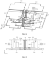
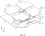
- FIG. 7 is a schematic diagram of a structure of an antenna element of an antenna-in-module according to an embodiment of this application.
- the antenna-in-module 200 provided in this embodiment of this application may include a ground plate 30, a first radiating element 21, a second radiating element 22, a third radiating element 23, a first feed stub 31, and a second feed stub 32.
- the first radiating element 21 and the ground plate 30 may be arranged at an interval along a Z-axis and are disposed opposite to each other.
- the first radiating element 21 and the second radiating element 22 may be arranged at an interval along an X-axis.
- a first gap C1 between the first radiating element 21 and the second radiating element 22 may extend along a Y-axis.
- the third radiating element 23 and the second radiating element 22 may be arranged at an interval along a Z-axis and are disposed opposite to each other.
- the first radiating element 21, the second radiating element 22, and the third radiating element 23 may be separately in a coupling connection to the ground plate 30.
- the antenna-in-module 200 provided in this embodiment of this application may further include a fourth radiating element 24.
- the fourth radiating element 24 may be disposed between the second radiating element 22 and the third radiating element 23, and the fourth radiating element 24 may be in a coupling connection to the ground plate 30.
- qualifiers related to a relative position relationship such as "being arranged along an X-axis" and "extending along a Y-axis", mentioned in embodiments of this application are not absolute and strict definitions in a mathematical sense.
- a small deviation is allowed, for example, may mean that being arranged in a direction approximate to the X-axis and extending in a direction approximate to the Y-axis are allowed.
- the approximation herein may be, for example, that a deviation angle is less than 10 degrees.
- a and B are arranged at an interval along an X-axis
- a and B are separately equivalent to a centrosymmetric pattern like a square or a circle
- respective equivalent center points of A and B are arranged at an interval along the X-axis.
- a connection line between the equivalent center points of A and B is located on the X-axis and the equivalent center points of A and B are spaced by a specific distance.
- the "gap” may be equivalent to a “narrow and long gap", and the "gap extending along a Y-axis” may be understood as that a length direction of the "narrow and long gap” is a Y-axis direction.
- a shape of the "gap” is not required herein.
- a width of the "gap” may be even or approximately even, and an edge of the "gap” may be, for example, a straight line or an irregular curve.
- the first radiating element 21 may include a first radiator 211 and a second radiator 212 that are arranged at an interval along the Y-axis, and a second gap C2 between the first radiator 211 and the second radiator 212 may extend along the X-axis.
- the second radiating element 22 may include a third radiator 221 and a fourth radiator 222 that are arranged at an interval along the Y-axis, and a third gap C3 between the third radiator 221 and the fourth radiator 222 may extend along the X-axis.
- the third radiating element 23 may include a fifth radiator 231 and a sixth radiator 232 that are arranged at an interval along the Y-axis, and a fourth gap C4 between the fifth radiator 231 and the sixth radiator 232 may extend along the X-axis.
- the fourth radiating element 24 may include a seventh radiator 241 and an eighth radiator 242, the seventh radiator 241 may be disposed between the third radiator 221 and the fifth radiator 231, and the eighth radiator 242 may be disposed between the fourth radiator 222 and the sixth radiator 232.
- the antenna-in-module 200 may further include: a first grounding element 351, a second grounding element 352, a third grounding element 361, and a fourth grounding element 362.
- the first grounding element 351 may be connected between the first radiator 211 and the ground plate 30, and the second grounding element 352 is connected between the second radiator 212 and the ground plate 30.
- the third grounding element 361 may be connected between the third radiator 221 and the ground plate 30, the third grounding element 361 may be connected to an end that is of the third radiator 221 and that faces the first radiator 211, the fourth grounding element 362 may be connected between the fourth radiator 222 and the ground plate 30, and the fourth grounding element 362 may be connected to an end that is of the fourth radiator 222 and that faces the second radiator 212.
- the seventh radiator 241 may be connected to the third grounding element 361, and the eighth radiator 242 may be connected to the fourth grounding element 362.
- the first feed stub 31 may be disposed in a first aperture (not marked in the figure), and the first aperture may include space between the first gap C1 and the ground plate 30.
- the first feed stub 31 may be electrically connected to a feed.
- the first feed stub 31 is configured to excite the first radiating element 21 and the second radiating element 22 to generate an electric field along the X-axis in the first aperture.
- the antenna-in-module 200 may further include a third feed stub 33 and a fourth feed stub 34.
- At least a part of the third feed stub 33 may be disposed in a third aperture (not marked in the figure), and the third aperture may include space between the second gap C2 and the third gap C3 and the ground plate 30.
- the third feed stub 33 may be electrically connected to the feed.
- the third feed stub 33 is configured to: excite the first radiating element 21 and the second radiating element 22 to generate an electric field along the Y-axis in the third aperture.
- the fourth feed stub 34 may include a first feed structure 341 and a second feed structure 342.
- the first feed structure 341 may be in a coupling connection to the seventh radiator 241, and the second feed structure 342 may be in a coupling connection to the eighth radiator 242.
- the first feed structure 341 and the second feed structure 342 may be electrically connected to the feed separately.
- the fourth feed stub 34 is configured to excite the seventh radiator 241 and the eighth radiator 242 to generate an electric field along the Y-axis.
- the "aperture” is a three-dimensional spatial structure.
- the "first aperture” not only includes the first gap C1 between the first radiating element 21 and the second radiating element 22, but also includes space that is of the first gap C1 and that faces a side of the ground plate 30, and may further include space that is of the first gap C1 and that is away from a side of the ground plate 30.
- the third radiating element 23 may be connected to the ground plate 30, or may be formed by using a partial structure of the ground plate 30. It should be understood that, in another embodiment, the third radiating element 23 may be disposed above or below the ground plate 30 (a positive direction of the Z-axis in the figure is the above), and is connected to the ground plate 30 by using a ground stub. In the following embodiments of this application, an embodiment in which the third radiating element 23 is used as a part of the ground plate 30 is used for description. In an embodiment, a part of a metal layer (for example, a metal layer located on an upper surface, or any metal layer used as the ground plate) of the substrate (for example, a PCB board) may be used as the third radiating element 23.
- a metal layer for example, a metal layer located on an upper surface, or any metal layer used as the ground plate
- the substrate for example, a PCB board
- the antenna-in-module 200 provided in the embodiment shown in FIG. 7 integrates a broadside antenna and an end-fire antenna.
- FIG. 7 completely shows four feed stubs, which are respectively feed structures used for the broadside antenna and the end-fire antenna.
- the solution included in FIG. 7 is not limited to one embodiment in which there are four feed stubs, and may further include a plurality of embodiments in which at least one feed stub is combined.
- the broadside antenna may include the first feed stub 31 and/or the third feed stub 33.
- the end-fire antenna may include the second feed stub 32 and/or the fourth feed stub 34.
- FIG. 7 completely shows a solution of vertical polarization of the broadside antenna, horizontal polarization of the broadside antenna, vertical polarization of the end-fire antenna, and horizontal polarization of the end-fire antenna.
- the solution corresponding to FIG. 7 is not limited to an embodiment of implementing both dual-polarization of the broadside antenna and dual-polarization of the end-fire antenna. In an embodiment of this application, the solution corresponding to FIG.
- FIG. 7 may be further split into an embodiment of implementing vertical polarization of a broadside antenna and horizontal polarization of the broadside antenna, an embodiment of implementing vertical polarization of an end-fire antenna and horizontal polarization of the end-fire antenna, an embodiment of implementing vertical polarization of a broadside antenna and vertical polarization of an end-fire antenna, an embodiment of implementing horizontal polarization of a broadside antenna horizontal polarization of an end-fire antenna, an embodiment of implementing single polarization of a broadside antenna, an embodiment of implementing single polarization of an end-fire antenna, or the like.
- These embodiments may be obtained based on FIG. 7 and a corresponding description of FIG. 7 , and all these embodiments should fall within the scope of this application.
- FIG. 8 provides an embodiment, obtained by splitting the embodiment of this application corresponding to FIG. 7 , of a broadside antenna.
- FIG. 9 provides an embodiment, obtained by splitting the embodiment of this application corresponding to FIG. 7 , of an end-fire antenna. It is not difficult to understand that the embodiment of the broadside antenna provided in FIG. 8 is not limited to an embodiment of implementing dual-polarization of the broadside antenna, and the embodiment of the end-fire antenna provided in FIG. 9 is not limited to an embodiment of implementing dual-polarization of the end-fire antenna.
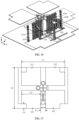
- FIG. 8 is a schematic diagram of a structure of a broadside antenna in an antenna-in-module according to an embodiment of this application.
- the broadside antenna provided in this embodiment of this application may include the ground plate 30, the first radiating element 21, the second radiating element 22, a first grounding element 351, a second grounding element 352, a third grounding element 352, a fourth grounding element 354, the first feed stub 31, and the third feed stub 33.
- the first radiating element 21 and the second radiating element 22 are main radiators of the broadside antenna.
- the ground plate 30 of the broadside antenna may be used to form at least a part of the third radiating element 23 in the end-fire antenna.
- the broadside antenna provided in an embodiment of this application may be a magneto electric dipole (magneto electric dipole) antenna having a dual-polarization characteristic.
- the first feed stub 31 is configured to: excite the first radiating element 21 and the second radiating element 22 to generate an electric field along the X-axis, and excite the broadside antenna to generate vertical polarization radiation.
- the third feed stub 33 is configured to: excite the first radiating element 21 and the second radiating element 22 to generate an electric field along the Y-axis, and excite the broadside antenna to generate horizontal polarization radiation.
- the vertical polarization direction mentioned herein is an X-axis direction
- the horizontal polarization direction is a Y-axis direction.
- the first feed stub 31 may extend along the X-axis, a projection of a first end of the first feed stub 31 on an XY plane may be located within a proj ection of the second gap C2 on the XY plane, and a projection of a second end of the first feed stub 31 on the XY plane may be located within a projection of the third gap C3 on the XY plane.
- the first feed stub 31 crosses the first gap C1, and two ends of the first feed stub 31 may be respectively in a coupling connection to the first radiating element 21 and the second radiating element 22.
- the first feed stub 31 may excite the first radiating element 21 and the second radiating element 22 to form vertical polarization radiation in the first aperture.
- the first gap C1 may include a first sub-gap C11 and a second sub-gap C12.
- the first sub-gap C11 is located between the first radiator 211 and the third radiator 221.
- the second sub-gap C12 is located between the second radiator 212 and the fourth radiator 222.
- the third feed stub 33 extends along the Y-axis.
- a projection of a first end of the third feed stub 33 on the XY plane is located within a projection of the first sub-gap C11 on the XY plane
- a projection of a second end of the third feed stub 33 on the XY plane is located within a projection of the second sub-gap C12 on the XY plane.
- the third feed stub 33 crosses a gap formed by the second gap C2 and the third gap C3, the first end of the third feed stub 33 may be in a coupling connection to the first radiator 211 and the third radiator 221, and the second end of the third feed stub 33 may be in a coupling connection to the second radiator 212 and the fourth radiator 222.
- the third feed stub 33 may excite the first radiating element 21 and the second radiating element 22 to form horizontal polarization radiation in the third aperture.
- the first radiating element 21 and the second radiating element 22 may be arranged at an interval along the X-axis.
- both the first radiating element 21 and the second radiating element 22 are metal layers, and may be disposed in a same plane, for example, both are parallel to the XY plane (a small deviation is allowed).
- a metal layer of the substrate 20 may form the first radiating element 21 and the second radiating element 22.
- the first radiating element 21 and the second radiating element 22 may be formed with the metal layer in the substrate 20 in a same process, to simplify a preparation process.
- the first feed stub 31 may be formed by using a metal layer, and may be disposed in a same plane, for example, parallel to the XY plane.
- a metal layer in which the first feed stub 31 is located may be coplanar with a metal layer in which the first radiating element 21 and the second radiating element 22 are located.
- the third feed stub 33 may be formed by using a metal layer, and may be disposed in a same plane, for example, parallel to the XY plane.
- the third feed stub 33 and the first feed stub 31 may be disposed in different metal layers in the substrate 20.
- the first grounding element 351 may be connected to a corner that is of the first radiator 211 and that is close to the second radiator 212 and the third radiator 221
- the second grounding element 352 may be connected to a corner that is of the second radiator 212 and that is close to the first radiator 211 and the fourth radiator 222.
- Both the first grounding element 351 and the second grounding element 352 may extend along the Z-axis, and are of a conductive connection hole structure.
- the third grounding element 361 may be of a metal wall structure, and the metal wall may be connected to a side that is of the third radiator 221 and that is close to the first radiator 211.
- the fourth grounding element 362 may be of a metal wall structure, and the metal wall may be connected to a side that is of the fourth radiator 222 and that is close to the second radiator 212.
- the metal wall may extend along the Z-axis, and is of a conductive connection hole structure.
- a width of the first gap C1 may be the same as a width of the second gap C2 and a width of the third gap C3.
- the first radiating element 21 and the second radiating element 22 may have a same area and shape.
- the first radiator 211, the second radiator 212, the third radiator 221, and the fourth radiator 222 may have a same area and shape, and are centrosymmetric.
- Shapes of the first radiator 211, the second radiator 212, the third radiator 221, and the fourth radiator 222 are not specifically limited in embodiments of this application. Shapes of all the four radiators may be set as a rectangle, or a rectangle with a missing corner shown in the figure. In an example, the four radiators have a same size and shape, and the shape of the radiator may be set as a square having a square missing corner. A spacing between any two radiators is the same, and the four radiators as a whole form a large square having a square missing corner in a positive direction at all four corners. It should be understood that an electrical length of the radiator may be increased by adding a missing corner to the radiator. It should be understood that a missing corner/recessed part or a protruding part of any shape may be disposed at any position of the radiator, and this should not be construed as a limitation on this application.
- the end-fire antenna provided in an embodiment of this application may be a magneto electric dipole (magneto electric dipole) antenna having a dual-polarization characteristic.
- the second feed stub 32 is configured to: excite the second radiating element 22 and the third radiating element 23 to generate an electric field along the Z-axis, and excite the end-fire antenna to generate vertical polarization radiation.
- the fourth feed stub 34 is configured to: excite the fourth radiating element 24 to generate an electric field along the Y-axis, and excite the end-fire antenna to generate horizontal polarization radiation.
- the vertical polarization direction mentioned herein is a Z-axis direction
- the horizontal polarization direction is a Y-axis direction.
- the second feed stub 32 may extend along the Z-axis, and an end of the second feed stub 32 is in a coupling connection to the second radiating element 22.
- the second feed stub 32 crosses the second aperture, a first end of the second feed stub 32 may be in a coupling connection to the third radiating element 23, and a second end of the second feed stub 32 may be connected to the second radiating element 22.
- the second feed stub 32 may excite the second radiating element 22 and the third radiating element 23 to form vertical polarization radiation in the second aperture.
- the second feed stub 32 may be of a conductive connection hole structure in the substrate 20.
- the conductive connection hole structure may be of a solid metal post structure formed by filling the connection hole with a metal material, or may be a metal layer formed after a metal material partially or completely covers a hole wall of the connection hole. All conductive connection holes in this specification may be understood as such.
- the second radiating element 22 and the third radiating element 23 may be two metal layers in different planes, for example, may be disposed in parallel and opposite to each other. In an embodiment, both the second radiating element 22 and the third radiating element 23 may be parallel to the XY plane (a small deviation is allowed).
- the second radiating element 22 and the third radiating element 23 have a same area and shape. In an embodiment, the second radiating element 22 and the third radiating element 23 are disposed opposite to each other. For example, an orthographic projection of the third radiating element 23 on the second radiating element 22 completely covers the second radiating element 22. In some other implementations, the second radiating element 22 and the third radiating element 23 may alternatively have different areas and/or shapes. In some other implementations, the second radiating element 22 and the third radiating element 23 may not be completely opposite to each other. For example, the second radiating element 22 and the third radiating element 23 may be partially opposite to each other.
- the fourth radiating element 24 may include a seventh radiator 241 and an eighth radiator 242 that are arranged at an interval along the Y-axis. In an embodiment, both the seventh radiator 241 and the eighth radiator 242 may be disposed perpendicular to the XY plane.
- the seventh radiator 241 and the eighth radiator 242 have a same area and shape, and may be designed in a mirror-symmetrical manner relative to the third aperture.
- the seventh radiator 241 and the eighth radiator 242 may be disposed perpendicular to the YZ plane.
- the seventh radiator 241 and the eighth radiator 242 may be disposed in parallel and opposite to each other.
- the seventh radiator 241 and the eighth radiator 242 may be disposed at an included angle relative to the YZ plane.
- the seventh radiator 241 and the eighth radiator 242 may not be parallel to each other.
- a first end of the seventh radiator 241 is connected to the third grounding element 361, a second end of the seventh radiator 241 extends toward a side away from the eighth radiator 242, a first end of the eighth radiator 242 is connected to the fourth grounding element 362, and a second end of the eighth radiator 242 extends toward a side away from the seventh radiator 241. That is, in a direction from X+ to X-, from a direction away from the first radiating element 21 to a direction close to the first radiating element 21, a distance between the seventh radiator 241 and the eighth radiator 242 in the Y direction may be gradually reduced.
- the fourth feed stub 34 may include a first feed structure 341 and a second feed structure 342. An end part of the first feed structure 341 may be in a coupling connection to the seventh radiator 241, and an end part of the second feed structure 342 may be in a coupling connection to the eighth radiator 242.
- the first feed structure 341 and the second feed structure 342 may carry differential signals, carry currents of a same magnitude and opposite phases, and implement excitation through non-connection capacitive coupling.
- the fourth feed stub 34 may form horizontal polarization radiation between the seventh radiator 241 and the eighth radiator 242 through excitation.
- the first feed structure 341 and the second feed structure 342 are of a metal wire structure as a whole, and may be formed by using a same metal layer in the substrate 20, to simplify a preparation process.
- a ground structure of the second radiating element 22 is the third grounding element 361 and the fourth grounding element 362. Details are not described herein again.
- the third radiating element 23 may be a part of the ground plate 30, and may be directly grounded.
- the seventh radiator 241 may be connected to the third grounding element 361, and the eighth radiator 242 may be connected to the fourth grounding element 362, to implement indirect grounding of the fourth radiating element 24.
- the second radiating element 22, the third grounding element 361, and the fourth grounding element 362 are reused and co-structured in the broadside antenna and the end-fire antenna provided in this embodiment of this application.
- the second radiating element 22 may be used as at least a part of the radiator of each of the broadside antenna and the end-fire antenna.
- the third grounding element 361 and the fourth grounding element 362 may be configured to be disconnected (for example, disconnected by turning off a switch) from the ground plate 30 in the broadside antenna, so that the second radiating element 22 is used as a radiator of the broadside antenna to radiate.
- the third grounding element 361 and the fourth grounding element 362 may be connected (for example, connected by turning on a switch) to the ground plate, so that the second radiating element 22 is turned on, to meet a radiation boundary condition of the end-fire antenna.
- the broadside antenna and the end-fire antenna may further reuse the third radiating element 23.
- the third radiating element 23 may be used as a reference ground of the broadside antenna and also be used as a radiator of the end-fire antenna. Therefore, the antenna-in-module provided in this embodiment of this application can greatly reduce an area in which the broadside antenna and the end-fire antenna are integrated while functions of the broadside antenna and the end-fire antenna are integrated.
- the antenna-in-module provided in this embodiment of this application can implement a dual-polarized broadside antenna and a dual-polarized end-fire antenna, to implement polarization diversity (polarization diversity) of the antenna-in-module 200, thereby helping improve a transmission throughput and signal stability of a weak-signal region, and meeting a signal transmission requirement.
- polarization diversity polarization diversity
- FIG. 10 is a schematic planar expanded view of an antenna-in-module according to an embodiment of this application.
- FIG. 11 is a topology diagram of a folded planar aperture structure of an antenna-in-module according to an embodiment of this application.
- FIG. 10 is a schematic diagram of slots between radiators obtained by spreading only the first radiating element 21, the second radiating element 22, and the third radiating element 23 into a planar structure without considering the ground plate 30, the first grounding element 35, and the second grounding element 36.
- the slots between the radiators are radiation apertures of the antenna-in-module 200.
- FIG. 11 is a schematic diagram of a three-dimensional radiation aperture structure obtained by folding a radiation aperture structure of a plane in FIG. 10 along a dashed line in FIG. 10 .
- BR_V refers to electric field distribution in a radiation aperture of a broadside antenna in a vertical polarization mode.
- BR_H refers to electric field distribution in a radiation aperture of the broadside antenna in a horizontal polarization mode.
- EF_V refers to electric field distribution in a radiation aperture of an end-fire antenna in the vertical polarization mode.
- EF_H refers to electric field distribution in a radiation aperture of the end-fire antenna in the horizontal polarization mode.
- the radiation aperture of the BR_V may be considered as the first aperture
- the radiation aperture of the BR_H may be considered as the third aperture
- the radiation aperture of the EF_V may be considered as the second aperture
- the radiation aperture of the EF_H may be considered as space between the third gap C3 and the fourth gap C4. It should be noted that the radiation aperture corresponding to BR_H overlaps with that corresponding to EF_H.
- electric fields between BR_V and BR_H are orthogonal, so that the dual-polarized broadside antenna is highly isolated and can be operated simultaneously.
- electric fields between EF_V and EF_H are orthogonal, so that the dual-polarized end-fire antenna is highly isolated and can be operated simultaneously.
- the antenna-in-module reuses the second radiating element in the broadside antenna and the second radiating element in the end-fire antenna, to implement an antenna radiation pattern re-configurable (Antenna Pattern Re-configurable) through circuit control, so that the radiation pattern of the antenna-in-module may be a pattern in a broadside direction or a pattern in an end-fire direction.
- the circuit control may be implemented by additionally disposing a switch in the antenna-in-module 200.
- a first switch SW1 and a second switch SW2 may be disposed in the antenna-in-module 200, and the first switch SW1 may be connected between the third grounding element 361 and the ground plate 30.
- the first switch SW1 is located on a side that is of the third grounding element 361 and that is away from the fourth radiator 222.
- the second switch SW2 may be connected between the fourth grounding element 362 and the ground plate 30.
- the second switch SW2 is located on a side that is of the fourth grounding element 362 and that is away from the third radiator 221.
- the first switch SW1 is configured to control whether to ground the third radiator 221
- the second switch SW2 is configured to control whether to ground the fourth radiator 222
- the first switch SW1 and the second switch SW2 are configured to control whether to ground the second radiating element 22.
- the first switch SW1 and the second switch SW2 are controlled to be turned on (turned on), so that the second radiating element 22 is grounded, to create a boundary condition in which electric fields on both sides in the radiation aperture of the EF_V are the smallest.
- the first switch SW1 and the second switch SW2 are controlled to be turned off (turned off), so that a main radiation aperture of the antenna-in-module 200 returns to the radiation aperture of the BR_V and the radiation aperture of the BR_H.
- a third switch SW3 and a fourth switch SW4 may be further disposed in the antenna-in-module 200.
- the third switch SW3 may be connected between the fifth radiator 231 and the sixth radiator 232.
- the third switch SW3 is located on a side that is of the third radiating element 23 and that is away from the first radiating element 21.
- the fourth switch SW4 may be connected between the third radiator 221 and the fourth radiator 222.
- the third switch SW3 is located on a side that is of the second radiating element 22 and that is close to the first radiating element 21.
- the third switch SW3 is configured to control turn-on or turn-on between the fifth radiator 231 and the sixth radiator 232
- the fourth switch SW4 is configured to control turn-on or turn-on between the third radiator 221 and the fourth radiator 222.
- the third switch SW3 When the antenna-in-module 200 is in a broadside mode, the third switch SW3 is controlled to be tuned on (turned on) and the fourth switch SW4 is controlled to be turned off (turned off).
- the third switch SW3 When the antenna-in-module 200 is in the end-fire mode, the third switch SW3 is controlled to be turned off (turned off) and the fourth switch SW4 is controlled to be turned on (turned on). In this way, pattern operations in the broadside mode and end-fire mode are achieved.
- all the first switch SW1, the second switch SW2, the third switch SW3, and the fourth switch SW4 may be disposed, to improve a pattern switching enhancement and an operation bandwidth.
- the switch usually has a parasitic resistance (Ron) while being turned on and a capacitance (Coff) while being turned off.
- Ron parasitic resistance
- Coff capacitance
- the third switch SW3 and the fourth switch SW4 are placed in a large electric field region of an antenna mode, to load the antenna mode.
- a capacitance of the third switch SW3 and a capacitance of the fourth switch SW4 are less than or equal to 10 fF.
- FIG. 12 is a schematic diagram of a structure of an antenna-in-module from another angle according to an embodiment of this application.
- hiding processing for example, a dashed line is used
- FIG. 12 a first end of the first feed stub 31 is connected to a first feed-in part 311, the first feed-in part 311 may be located on a side that is of the first feed stub 31 and that faces the ground plate 30, and the first feed-in part 311 may extend along the Z-axis and be connected to a feed (not shown in the figure).
- the first feed stub 31 is a vertically polarized feed stub of the broadside antenna.
- the first feed-in part 311 may be electrically connected to a radio frequency port of the transmitter and/or receiver chip 105, to implement a connection to the feed.
- the electrical connection may be implemented, for example, by using a feeder like a microstrip.
- the first feed stub 31 and the first feed-in part 311 may be considered as a " ⁇ " type as a whole.
- a first end of the third feed stub 33 is connected to a second feed-in part 331, the second feed-in part 331 may be located on a side that is of the third feed stub 33 and that faces the ground plate 30, and the second feed-in part 331 may extend along the Z-axis and be connected to the feed.
- the third feed stub 33 is a horizontally polarized feed stub of the broadside antenna.
- the second feed-in part 331 may be electrically connected to a radio frequency port of the transmitter and/or receiver chip 105, to implement a connection to the feed.
- the electrical connection may be implemented, for example, by using a feeder like a microstrip.
- the third feed stub 33 and the second feed-in part 331 may be considered as a " ⁇ " type as a whole.
- the first feed stub 31 and the third feed stub 33 are disposed orthogonally and are insulated from each other.
- the first feed stub 31 and the third feed stub 33 may be disposed in different metal layers in the substrate 20.
- the first feed stub 31 may be located in a same metal layer with the first radiator 211, the second radiator 212, the third radiator 221, and the fourth radiator 222, to simplify a preparation process.
- the third feed stub 33 may be located in another metal layer below (a positive direction of the Z-axis is defined as below, and a negative direction of the Z-axis is defined as above) the first feed stub 31, and an insulation layer is disposed between the two metal layers.
- first feed-in part 311 and the second feed-in part 331 are presented as columnar structures in the figure, to facilitate intuitive understanding of the accompanying drawings. It should be understood that, the first feed-in part 311 and the second feed-in part 331 may be of a conductive connection hole structure in the substrate 20.
- the conductive connection hole structure may be of a solid metal post structure formed by filling the connection hole with a metal material, or may be a metal layer formed after a metal material partially or completely covers a hole wall of the connection hole.
- FIG. 13 is a side view of an antenna-in-module according to an embodiment of this application.
- the first grounding element 351 may include a first ground segment 3511, a second ground segment 3512, and a third ground segment 3513 that are sequentially connected.
- the first ground segment 3511 is connected to the first radiator 211
- the third ground segment 3513 is connected to the ground plate 30, and the first ground segment 3511 and the third ground segment 3513 may extend along the Z-axis and are of a conductive connection hole structure.
- the second ground segment 3512 may extend along the XY plane, and is formed by using a part of the metal layer in the substrate 20.
- the first grounding element 351 includes three bent segments as a whole, and a total electrical length of the first grounding element 351 is 1/4 ⁇ .
- the first grounding element 351 is disposed as a multi-segment bent structure, which helps reduce a height between the first radiator 211 and the ground plate 30, thereby reducing an overall size of the antenna-in-module 200.
- a position of the first grounding element 351 is not specifically limited in this application.
- the first ground segment 3511 may be connected to a corner that is of the first radiator 211 and that is close to the second radiator 212 and the third radiator 221, and orthographic projections of the second ground segment 3512 and the third ground segment 3513 on the first radiator 211 are located inside the first radiator 211, to prevent the second ground segment 3512 and the third ground segment 3513 from interfering with the first feed-in part 311.
- both the first grounding element 351 and the second grounding element 352 may be of conductive connection hole structures extending along the Z-axis, and a total electrical length of the first grounding element 351 and the second grounding element 352 meets 1/4 ⁇ .
- neither the first grounding element 351 nor the second grounding element 352 has a bent segment, so that a ground structure design can be simplified.
- FIG. 14 is a schematic diagram of a structure of an antenna-in-module from another angle according to an embodiment of this application.
- hiding processing for example, a dashed line is used
- one end of the second feed stub 32 may be connected to a feed (not marked in the figure)
- the other end of the second feed stub 32 may be connected to a connection stub 321
- the connection stub 321 may be connected between the third radiator 221 and the fourth radiator 222.
- the second feed stub 32 is a vertically polarized feed stub of the end-fire antenna, and the connection stub 321 is configured to implement direct feeding of the second feed stub 32 and the second radiating element 22.
- the second feed stub 32 may be of a conductive connection hole structure in the substrate 20, and the connection stub 321 may be disposed in a metal layer in the substrate 20.
- the connection stub 321 may be located in a same metal layer with the first feed stub 31, the first radiator 211, the second radiator 212, the third radiator 221, and the fourth radiator 222, to simplify a preparation process.
- the fourth feed-in part 3411, the fourth feed part 3413, the fifth feed-in part 3421, and the fifth feed part 3423 may extend along the X-axis, and the first connection part 3412 and the second connection part 3422 may extend along the Y-axis.
- the first feed structure 341 and the second feed structure 342 are of a metal wire structure as a whole, and may be formed by using a same metal layer in the substrate 20, to simplify a preparation process.
- the fourth feed stub 34 is a horizontally polarized feed stub of the end-fire antenna, and is a coupling capacitor type excitation structure.
- the fourth feed stub 34 is disposed between the second radiating element 22 and the third radiating element 23, and differential signals are carried on the first feed structure 341 and the second feed structure 342 to carry currents of a same magnitude and opposite phases, to implement excitation through non-connection capacitive coupling.
- the fourth feed stub 34 performs excitation near the fourth radiating element 24, and the fourth radiating element 24 is excited in a coupled feed-in manner, so that a loss caused by impedance mismatching can be avoided, and radiation efficiency of the end-fire antenna can be improved.
- differential characteristic impedance of the fourth feed stub 34 is adjusted by adjusting linewidths and a spacing of the first feed structure 341 and the second feed structure 342.
- the fourth feed stub 34 further includes a parasitic element 343.
- the parasitic element 343, the first feed structure 341, and the second feed structure 342 are coplanar.
- the parasitic element 343 is disposed on a side that is of the first feed structure 341 and the second feed structure 342 and that is away from the seventh radiator 241 and the eighth radiator 242, and is disposed at an interval with the first feed structure 341 and the second feed structure 342.
- the parasitic element 343 extends along the Y-axis, and is parallel to and disposed at an interval with the first connection part 3412 and the second connection part 3422.
- the parasitic element 343, the first feed structure 341, and the second feed structure 342 are formed by using a same metal layer in the substrate 20, to simplify a preparation process.
- the parasitic element 343 may strengthen a differential mode of differential currents carried on the first feed structure 341 and the second feed structure 342, and suppress a common mode of a codirectional current, to ensure that a horizontally polarized antenna mode of the end-fire antenna is excited.
- FIG. 15 is a side view of an antenna-in-module from another angle according to an embodiment of this application.
- the third grounding element 361 may include a first ground wall 361a and a second ground wall 361b.
- the first ground wall 361a and the second ground wall 361b are respectively connected to the third radiator 221 at a first position and a second position, and the first position and the second position are arranged at an interval on the third radiator 221.
- the first ground wall 361a is located on a side that is of the third radiator 221 and that is close to the fourth radiator 222, the seventh radiator 241 is connected to the first ground wall 361a, and the first switch SW1 is connected between the second ground wall 361b and the ground plate 30.
- the fourth grounding element 362 may include a third ground wall 362a and a fourth ground wall 362b.
- the third ground wall 362a and the fourth ground wall 362b are respectively connected to the fourth radiator 222 at a third position and a fourth position.
- the third position and the fourth position are arranged at an interval on the fourth radiator 222.
- the third ground wall 362a is located on a side that is of the fourth radiator 222 and that is close to the third radiator 221
- the eighth radiator 242 is connected to the third ground wall 362a
- the second switch SW2 is connected between the fourth ground wall 362b and the ground plate 30.
- the hollow-out region is used to reduce unnecessary resonance, and a size of the hollow-out region is not specifically limited in embodiments of this application.
- a width of the first ground wall 361a may be greater than a width of the second ground wall 361b, and the first switch SW1 may be connected to the second ground wall 361b.
- a width of the third ground wall 362a may be greater than a width of the fourth ground wall 362b, and the second switch SW2 may be connected to the fourth ground wall 362b.
- the third ground wall 362a may include a fourth ground segment 3621, a fifth ground segment 3622, and a sixth ground segment 3623 that are sequentially connected.
- the fourth ground segment 3621 is connected to the fourth radiator 222
- the sixth ground segment 3623 is connected to the ground plate 30.
- the fourth ground segment 3621 and the sixth ground segment 3623 may extend along the Z-axis, and are of conductive connection hole structures.
- the fifth ground segment 3622 may extend along the XY plane, and is formed by using a part of a metal layer in the substrate 20.
- the third ground wall 362a includes three bent segments as a whole, and a total electrical length of the third ground wall 362a is 1/4 ⁇ .
- the third ground wall 362a is disposed as a multi-segment bent structure, which helps reduce a height between the fourth radiator 222 and the ground plate 30, thereby reducing an overall size of the antenna-in-module 200.
- first ground wall 361a and the third ground wall 362a may be the same in structure, and are axisymmetrically disposed relative to the third aperture.
- the structure of the first ground wall 361a is not described herein again.
- the first ground wall 361a and the third ground wall 362a may be of conductive connection hole structures extending along the Z-axis, and a total electrical length of the first ground wall 361a and the third ground wall 362a meets 1/4 ⁇ .
- the first ground wall 361a nor the third ground wall 362a has a bent segment, so that a structure design can be simplified.
- FIG. 16 is a schematic diagram of a structure of a metal wall according to an embodiment of this application.
- the ground walls 361a, 361b, 362a, and 362b, and the radiators 241 and 242 are of a metal wall structure as a whole.
- the metal wall may include a plurality of conductive connection holes, and there may be intervals between the plurality of conductive connection holes.
- the plurality of conductive connection holes may communicate with each other by using a metal layer.
- Each conductive connection hole structure may be of a solid metal post structure formed by filling the connection hole with a metal material, or a metal layer formed after a metal material partially or completely covers a hole wall of the connection hole.
- the metal wall structure may be a complete wall structure.
- the complete wall structure may be of a solid metal post structure formed after a metal material is filled into an elongated cavity, or may be a metal layer formed after a metal material partially or completely covers an inner wall of an elongated cavity.
- the antenna-in-module provided in embodiments of this application may support a millimeter-wave band, for example, a 5G millimeter-wave band.
- a length and a width of an antenna element may be, for example, less than 4 mm, and a thickness of the antenna element may be less than 1.5 mm.
- FIG. 17 is a schematic top view of an antenna-in-module according to an embodiment of this application.
- a distance H1 between the first radiating element 21 and the ground plate 30 may be 0.9 mm
- a distance H2 between the second radiating element 22 and the ground plate 30 may be 1.05 mm
- a length L1 of the first radiating element 21 may be 3.5 mm
- a length L2 of the second radiating element 22 may be 3.5 mm.
- All the six radiating elements may be shaped like a square with a missing corner, a side length L3 of the square may be 1.55 mm, the missing corner may be shaped like a square, and a width L4 of the missing corner may be 0.4 mm.
- the first gap C1, the second gap C2, the third gap C3, and the fourth gap C4 may have a same width, and a width L5 of the gap may be 0.4 mm.
- the foregoing antenna elements with a size of 3.5*3.5*1.05 mm 3 are arranged as the antenna-in-module 200 shown in FIG. 4 .
- the first switch SW1 and the second switch SW2 are controlled to be turned on or turned off to excite the antenna-in-module 200 with a broadside dual-polarized feed stub or an end-fire dual-polarized feed stub, to obtain a radiation gain pattern of the antenna-in-module 200.
- FIG. 18 is a radiation gain pattern of an antenna-in-module according to an embodiment of this application.
- the broadside antenna and the end-fire antenna are co-structured.
- FIG. 19 is a diagram of a cumulative distribution function of an antenna gain of an antenna-in-module according to an embodiment of this application.
- A1 and A2 represent antenna gains of the conventional technology in which only a broadside antenna is disposed.
- B1 and B2 represent specific quantized antenna gains obtained after the antenna-in-module 200 is applied to the electronic device 100 and arranged based on the position in FIG. 5 in this application.
- A1 and B1 represent a frequency of -27 GHZ
- A2 and B2 represent a frequency of -40 GHZ.
- 20% CDF is an important indicator for observing weak field strength under the operator's specification
- 50% CDF is an important indicator for observing weak field strength under the 3GPP specification. As shown in FIG.
- Table 1 shows antenna gain data of the antenna-in-module according to an embodiment of this application
- Table 2 shows data of an antenna coverage angle of the antenna-in-module according to an embodiment of this application.
- a gain in the +Z direction may be 4.2 dB.
- a gain in the +Z direction is only -2.0 dB. Therefore, a switching enhancement of 6.2 dB may be obtained in the +Z direction through pattern switching.
- a gain in the +X direction is only -3.8 dB. However, if the operation is switched to the end-fire mode, a gain of 2.9 dB may be obtained. Therefore, a switching enhancement of 6.7 dB may be obtained in the +X direction through pattern switching.
- a gain coverage angle of the conventional technology in which only a broadside antenna is available is 120°.
- the coverage angle can be expanded to 270° by switching between the broadside mode and the end-fire mode. Therefore, compared with the conventional technology, this application has an enhancement of 150° in coverage angle.
- FIG. 18 to FIG. 20 show effect of the antenna-in-module 200 according to an embodiment of this application in an implementation.
- the antenna-in-module 200 is a dual-polarized pattern-switchable co-structured broadside and end-fire antenna.
- the antenna-in-module 200 may include four radiating elements 21 to 24, four feed stubs 31 to 34, and two switches SW1 and SW2. By switching through the switch and selecting the feed stub, the antenna-in-module may be used to implement a dual-polarized broadside radiation pattern or a dual-polarized end-fire radiation pattern.
- FIG. 21 is another schematic diagram of a structure of an antenna-in-module according to an embodiment of this application.
- the antenna-in-module 200 may be a vertically polarized dual-band antenna.
- the antenna-in-module 200 may include three radiating elements 21 to 23, the first feed stub 31, and the second feed stub 33, and include only a broadside vertically polarized antenna and an end-fire vertically polarized antenna.
- the broadside antenna may support both a low-frequency band and a high-frequency band, and the end-fire antenna may also support both a low-frequency band and a high-frequency band.
- the broadside vertically polarized antenna and the end-fire vertically polarized antenna refer to the description of the dual-polarized pattern-switchable co-structured broadside and end-fire antenna. Details are not described herein again.
- FIG. 22a is a diagram of a broadside and end-fire vertical polarization radiation gain pattern of the antenna-in-module provided in FIG. 21 in a low-frequency band
- FIG. 22b is a diagram of a broadside and end-fire vertical polarization radiation gain pattern of the antenna-in-module provided in FIG. 21 in a high-frequency band.
- the low-frequency band is a 29.0 GHz frequency band
- the high-frequency band is a 39.0 GHz frequency band.
- an operation in an end-fire mode may have a switching enhancement of 5.5 dB.
- an operation in the broadside mode may have a switching gain of 8.9 dB.
- an operation in an end-fire mode may have a switching enhancement of 5.8 dB.
- an operation in the end-fire mode may have a switching gain of 6.2 dB.
- FIG. 23 is another schematic diagram of a structure of an antenna-in-module according to an embodiment of this application.
- the antenna-in-module 200 may be a horizontally polarized dual-band antenna.
- the antenna-in-module 200 may include four radiating elements 21 to 24, the second feed stub 32, and the fourth feed stub 34, and include only a broadside horizontally polarized antenna and an end-fire horizontally polarized antenna.
- the broadside antenna may support both a low-frequency band and a high-frequency band, and the end-fire antenna may also support both a low-frequency band and a high-frequency band.
- the broadside horizontally polarized antenna and the end-fire horizontally polarized antenna refer to the description of the dual-polarized pattern-switchable co-structured broadside and end-fire antenna. Details are not described herein again.
- FIG. 24a is a diagram of a broadside and end-fire horizontal polarization radiation gain pattern of the antenna-in-module provided in FIG. 23 in a low-frequency band
- FIG. 24b is a diagram of a broadside and end-fire horizontal polarization radiation gain pattern of the antenna-in-module provided in FIG. 23 in a high-frequency band.
- the low-frequency band is a 29.0 GHz frequency band
- the high-frequency band is a 39.0 GHz frequency band.
- an operation in a broadside mode may have a switching enhancement of 5 dB.
- an operation in a broadside mode may have a switching enhancement of 7.0 dB.
- an operation in the end-fire mode may have a switching gain of 2.0 dB.
- the antenna-in-module provided in embodiments of this application may be a dual-polarized pattern-switchable co-structured broadside and end-fire antenna, or may be a vertically polarized dual-band antenna, or may be a horizontally polarized dual-band antenna.
- the antenna-in-module provided in embodiments of this application can obtain an obvious antenna gain.
- the second radiating elements in the broadside antenna and the end-fire antenna are reused, to implement an antenna radiation pattern re-configurable through circuit control, so that the radiation pattern of the antenna-in-module may be a broadside pattern or an end-fire pattern, and the antenna-in-module supports dual-polarization in both radiation models.
- the antenna-in-module provided in embodiments of this application may be placed on a side of an electronic device without increasing an antenna area, and may further increase a radiation gain and a signal coverage angle.
- the antenna-in-module provided in embodiments of this application can reduce an antenna area by at least 30%.
- the antenna-in-module 200 provided in embodiments of this application is a millimeter-wave antenna module applied to a mobile phone. It should be understood that the antenna-in-module 200 provided in embodiments of this application may not be limited to being applied to the millimeter-wave antenna module. For example, the antenna-in-module 200 provided in embodiments of this application may be further applied to a base station antenna, a Wi-Fi sharer antenna, a head-mounted apparatus antenna, a spatial positioning antenna, a UWB (Ultra-Wideband, ultra-wideband) antenna, an IOT (Internet of Things, Internet of Things) antenna, and the like.
- a base station antenna a Wi-Fi sharer antenna
- a head-mounted apparatus antenna a spatial positioning antenna
- UWB Ultra-Wideband, ultra-wideband
- IOT Internet of Things, Internet of Things
- the antenna-in-module 200 provided in embodiments of this application may be applied to a base station antenna.
- each antenna element in the base station antenna can increase a radiation pattern in an end-fire direction without increasing the original area, so that a signal coverage range of a base station is effectively increased, or a quantity of base station antennas is reduced.
- the antenna-in-module 200 provided in embodiments of this application may be applied to a ceiling-mounted or wall-mounted Wi-Fi sharer antenna.
- the broadside antenna radiation pattern can be connected to a user, or switched to the end-fire direction, to form a mesh grid with another home IOT appliance and another Wi-Fi sharer, so that indoor signal coverage is improved.
Landscapes
- Engineering & Computer Science (AREA)
- Computer Networks & Wireless Communication (AREA)
- Microelectronics & Electronic Packaging (AREA)
- Variable-Direction Aerials And Aerial Arrays (AREA)
- Details Of Aerials (AREA)
Applications Claiming Priority (2)
| Application Number | Priority Date | Filing Date | Title |
|---|---|---|---|
| CN202111649196.3A CN116417780B (zh) | 2021-12-29 | 2021-12-29 | 天线结构、封装天线、芯片和电子设备 |
| PCT/CN2022/137702 WO2023124887A1 (zh) | 2021-12-29 | 2022-12-08 | 天线结构、封装天线、芯片和电子设备 |
Publications (2)
| Publication Number | Publication Date |
|---|---|
| EP4435969A1 true EP4435969A1 (de) | 2024-09-25 |
| EP4435969A4 EP4435969A4 (de) | 2025-04-09 |
Family
ID=86997637
Family Applications (1)
| Application Number | Title | Priority Date | Filing Date |
|---|---|---|---|
| EP22914142.9A Pending EP4435969A4 (de) | 2021-12-29 | 2022-12-08 | Antennenstruktur, antenne in gehäuse, chip und elektronische vorrichtung |
Country Status (4)
| Country | Link |
|---|---|
| US (1) | US20250087906A1 (de) |
| EP (1) | EP4435969A4 (de) |
| CN (1) | CN116417780B (de) |
| WO (1) | WO2023124887A1 (de) |
Families Citing this family (3)
| Publication number | Priority date | Publication date | Assignee | Title |
|---|---|---|---|---|
| US20250233310A1 (en) * | 2024-01-17 | 2025-07-17 | Advanced Semiconductor Engineering, Inc. | Electronic device |
| CN121055030A (zh) * | 2024-05-29 | 2025-12-02 | 明泰科技股份有限公司 | 磁电偶极天线及天线阵列 |
| GB2643461A (en) * | 2024-08-14 | 2026-02-18 | Chelton Ltd | Antenna |
Family Cites Families (11)
| Publication number | Priority date | Publication date | Assignee | Title |
|---|---|---|---|---|
| US9819098B2 (en) * | 2013-09-11 | 2017-11-14 | International Business Machines Corporation | Antenna-in-package structures with broadside and end-fire radiations |
| CN108183324A (zh) * | 2014-08-12 | 2018-06-19 | 启碁科技股份有限公司 | 天线及天线模块 |
| KR20190087270A (ko) * | 2018-01-15 | 2019-07-24 | 엘지전자 주식회사 | 무선 통신 시스템에서 안테나 장치 및 이를 구비하는 전자기기 |
| DE102019107258A1 (de) * | 2018-05-24 | 2019-11-28 | Samsung Electronics Co., Ltd. | Phased-array-antennenmodul und kommunikationsvorrichtung mit demselben |
| CN112805878B (zh) * | 2018-10-10 | 2022-05-24 | 华为技术有限公司 | 天线、无线装置及天线阵列 |
| US11005184B2 (en) * | 2018-11-29 | 2021-05-11 | Samsung Electro-Mechanics Co., Ltd. | Antenna apparatus |
| KR102505199B1 (ko) * | 2018-12-19 | 2023-02-28 | 삼성전기주식회사 | 고주파 필터 모듈 |
| CN113678318B (zh) * | 2019-05-31 | 2022-12-30 | 华为技术有限公司 | 一种封装天线装置及终端设备 |
| CN211428346U (zh) * | 2019-10-31 | 2020-09-04 | Oppo广东移动通信有限公司 | 天线模组及电子设备 |
| CN111326856B (zh) * | 2020-02-24 | 2022-07-26 | 华南理工大学 | 一种基于准pifa天线的超低剖面端射垂直极化天线 |
| CN113594711A (zh) * | 2020-04-30 | 2021-11-02 | 华为技术有限公司 | 垂直极化天线及电子设备 |
-
2021
- 2021-12-29 CN CN202111649196.3A patent/CN116417780B/zh active Active
-
2022
- 2022-12-08 US US18/724,559 patent/US20250087906A1/en active Pending
- 2022-12-08 EP EP22914142.9A patent/EP4435969A4/de active Pending
- 2022-12-08 WO PCT/CN2022/137702 patent/WO2023124887A1/zh not_active Ceased
Also Published As
| Publication number | Publication date |
|---|---|
| CN116417780B (zh) | 2026-01-06 |
| EP4435969A4 (de) | 2025-04-09 |
| CN116417780A (zh) | 2023-07-11 |
| US20250087906A1 (en) | 2025-03-13 |
| WO2023124887A1 (zh) | 2023-07-06 |
Similar Documents
| Publication | Publication Date | Title |
|---|---|---|
| CN110137675B (zh) | 一种天线单元及终端设备 | |
| EP4435969A1 (de) | Antennenstruktur, antenne in gehäuse, chip und elektronische vorrichtung | |
| EP2608315B1 (de) | Antennenvorrichtung mit schaltbarer Diversität, und Verfahren | |
| US11258177B2 (en) | Antenna unit, array antenna, and electronic device | |
| US12531331B2 (en) | Antenna structure and electronic device | |
| US20260031540A1 (en) | Antenna, antenna array, and electronic device | |
| CA2914269A1 (en) | Multiple-antenna system and mobile terminal | |
| EP2628208B1 (de) | Antennenpaar für mimo/diversitätsbetrieb in lte/gsm-frequenzbändern | |
| JP2007533193A (ja) | 2つのmemsスイッチ切替pifaを有する平面アンテナアセンブリ | |
| CN113013596A (zh) | 天线装置、壳体及电子设备 | |
| WO2023061128A9 (zh) | 谐振腔天线及电子设备 | |
| EP4340127A1 (de) | Breitseitenantenne, gehäuseantenne und kommunikationsvorrichtung | |
| WO2024063925A1 (en) | Substrate integrated waveguide cavity-backed dual-polarized multi-band antenna | |
| US10770798B2 (en) | Flex cable fed antenna system | |
| WO2021104191A1 (zh) | 天线单元及电子设备 | |
| CN114389005A (zh) | 一种电子设备 | |
| CN110828985A (zh) | 一种天线单元及电子设备 | |
| CN118841752A (zh) | 具有多基板堆叠贴片天线的电子设备 | |
| US20240304998A1 (en) | Electronic device | |
| CN110808455A (zh) | 一种天线单元及电子设备 | |
| CN113013595A (zh) | 天线装置、壳体及电子设备 | |
| EP4443648A1 (de) | Antenne und elektronische vorrichtung | |
| CN110828986A (zh) | 一种天线单元及电子设备 | |
| CN110808454A (zh) | 一种天线单元及电子设备 | |
| CN116780158A (zh) | 天线组件以及电子设备 |
Legal Events
| Date | Code | Title | Description |
|---|---|---|---|
| STAA | Information on the status of an ep patent application or granted ep patent |
Free format text: STATUS: THE INTERNATIONAL PUBLICATION HAS BEEN MADE |
|
| PUAI | Public reference made under article 153(3) epc to a published international application that has entered the european phase |
Free format text: ORIGINAL CODE: 0009012 |
|
| STAA | Information on the status of an ep patent application or granted ep patent |
Free format text: STATUS: REQUEST FOR EXAMINATION WAS MADE |
|
| 17P | Request for examination filed |
Effective date: 20240619 |
|
| AK | Designated contracting states |
Kind code of ref document: A1 Designated state(s): AL AT BE BG CH CY CZ DE DK EE ES FI FR GB GR HR HU IE IS IT LI LT LU LV MC ME MK MT NL NO PL PT RO RS SE SI SK SM TR |
|
| REG | Reference to a national code |
Ref country code: DE Ref legal event code: R079 Free format text: PREVIOUS MAIN CLASS: H01Q0001360000 Ipc: H01Q0001220000 |
|
| A4 | Supplementary search report drawn up and despatched |
Effective date: 20250311 |
|
| DAV | Request for validation of the european patent (deleted) | ||
| DAX | Request for extension of the european patent (deleted) | ||
| RIC1 | Information provided on ipc code assigned before grant |
Ipc: H01Q 1/48 20060101ALI20250305BHEP Ipc: H01Q 1/38 20060101ALI20250305BHEP Ipc: H01Q 1/24 20060101ALI20250305BHEP Ipc: H01Q 9/04 20060101ALI20250305BHEP Ipc: H01Q 21/24 20060101ALI20250305BHEP Ipc: H01Q 21/08 20060101ALI20250305BHEP Ipc: H01Q 9/28 20060101ALI20250305BHEP Ipc: H01Q 1/52 20060101ALI20250305BHEP Ipc: H01Q 21/28 20060101ALI20250305BHEP Ipc: H01Q 1/22 20060101AFI20250305BHEP |